FR-1 0116 AD-A238 8189 gab i end maiuitlsri data=edd.an c: f etmng and revi~ewing the tIjectiOri of...
119
FR-1 0116 AD-A238 818 5< 0 APPROVED FOR PUBLIC RELEASE DISTRIBUTION UNLIMITED 91-05:555 spire Hilt!1 Ill1Illt i1
Transcript of FR-1 0116 AD-A238 8189 gab i end maiuitlsri data=edd.an c: f etmng and revi~ewing the tIjectiOri of...

FR-1 0116
AD-A238 818
5< 0
APPROVED FOR PUBLIC RELEASE
DISTRIBUTION UNLIMITED
91-05:555 spireHilt!1 Ill1Illt i1

Form AppovedREPORT DOCUMENTATION PAGE CI0MB No. 0704-0188
Putific report ng ouroefo r this cooectioE of informhation Is estImated to average I hour per response, including the timie for revi~ewing instructionsl. searChing exusting data sources
9 gab i end maiuitlsri data=edd.an c: f etmng and revi~ewing the tIjectiOri of information. Send commuru~t regsarding this burden estimate Of any other aspect of Ibiscole4ton Ehnfrinmatiol.I nhg wglli oreding this burdeni. to Washingt001 Headquarters Services. Directorate for information Operations and Reports. 1275S iremonDavns mighiwV. Sute 1204, Arlington. VA 22202-4302. and to the Office of Managment and Budgeot.11Paperwork Reduction Protect(0704-138). Wa-lsnton. DC 20503
1. AGENCY USE ONLY (Leave blanlk) 2. REPORT DATE 3. REPORT TYPE AND DATES COVERED
1 19 April 1991 I _____________
4. TITLE AND SUBTITLE S. FUNDING NUMBERS
Deposition of InP-on-Si Substrates for MonolithicIntegration of Advanced Electronics D~i-0-
6. AUTHOR(S)
Stanley M. Vernon
7. PERFORMING ORGANIZATION NAME(S) AND AODRESS(ES) 8. PERFORMING ORGANIZATIONREPORT NUMBER
Spire CorporationOne Patriots ParkBedford, MA 01730-2396
9. SPONSORING/ MONITORING AGENCY NAME(S) AND ADDRESS(ES) 10. SPONSORING/ MONITORING
U. S. Army Research Office AEC EOTNME
P. 0. Box 12211Research Triangle Park, NC 27709-2211 0~ S /~~
11. SUPPLEMENTARY NOTES
The view, opinions and/or findings contained in this report are those of theauthor(s) and should not be construed as an official Department of the Armyposition, policy,_or decision, unless so designated by other documentation.-
12a. DISTP.BUTICN/ IAtVA!LA8IUTY STA TEW HT 1 2L%. DISTRIBUTION CODE
Approved for public release; distribution unlimited. j13. ABSTRACT (Maximum 200 words)
This report describes the development of a technology for the deposition of InP and lattice-matched InGaAs onto Si and GaAs substrates. Such structures are useful for the monolithicintegration of high-speed optical and electronic devices. The growth technique employed in thisprogram is metalorganic chemical vapor deposition (MOCYD), and GaAs buffer layers armemployed to improve the quality of the InP epilayers. Other defect-reduction techniques studiedinclude the use of strained layers and thermal annealing. Characterization methods includetransmission electron microscopy, double -crystal X-ray rocking curve analysis, Nornarskiinterference-contrast microscopy, photoluminescence (PL), PL decay, Hall effect, electrochemicalC-V profiling, and deep-level transient spectroscopy. Junction field-effect transistors and PINphotodiodes have been fabricated and characterized on Si, GaMs, and InP substrates, and theirperformance characteristics compared.
1% SUBJIECT TERMS 'IS. NUMBER OF PAGES46
InP, InGaAs, heteroepitaxy, MOCVD 16. PRIC ODE
17. SECURITY CLASSIFICATION 18. SECURITY CLASSIFICATION lB. SECURITY CLASSIFICATION 20. LIMITATION OF ABSTRACTOF REPORT OF THIS PAGE OF ABSTRACT
UNCLAS SIFIED UNCLASSIFIED UNCLASSIFIED ULNSN 7540-01-280-5500 Standard Form 298 (Rev 2-49
293-102 Wp ANSI Sid 239-13

GENERAL INSTRUCTIONS FOR COMPLETING SF 298
The Report Documentation Page (RDP) is used in announcing and cataloging reports. It is importantthat this informazlon be consistent with the rest of the report, particularly the cover and title page.Instructions for filling in each block of the form follow. It is important to stay within the lines to meetoptical scanning requirements.
Block 1. Agency Use Only (Leave blank). Block 12a. Distribution/Availability Statement.Denotes public availability or limitations. Cite any
Block 2. Report Date. Full publication date availability to the public. Enter additionalincluding day, month, and year, if available (e.g. 1 limitations or special markings in all capitals (e.g.Jan 88). Must cite at least the year. NOFORN, REL, ITAR).
Block 3. Type of Report and Dates Covered. DOD - See DODD 5230.24, DistributionState whether report is interim, final, etc. If Statements on Technical applicable, enter inclusive report dates (e.g. 10 Documents. *Jun 87 - 30 Jun 88). DOE - See authorities.
Block 4. Title and Subtitle. A title is taken from NASA - See Handbook NHB 2200.2.the part of the report that provides the most NTIS - Leave blank.meaningful and complete information. When areport is prepared in more than one volume, Block 12b. Disribution Code.repeat the primary title, add volume number, andinclude subtitle for the specific volume. Onclassified documents enter the title classification DOE - Eae blank.in parentheses. DOE - Enter DOE distribution categories
from the Standard Distribution for
Block 5. Funding Numbers To include contract Unclassified Scientific and Technicaland grant numbers; may inc, ude program Reports.element number(s), project rumber(s), task NASA - Leave blank.number(s), and work unit number(s). Use the NTIS - Leave blank.
following labels:
C - Contract PR Project Block 13. Abstract. Include a brief (Maximum- Grant TA Task 200 words) factual summary of the most
PE - Program WU - Work Unit significant information contained in the report.Element Accession No.
Block 6. Author(s). Name(s) of person(s) Block 14. Subiect Terms. Keywords or phrasesresponsible for writing the report, performing identifying major subjects in the report.the research, or credited with the content of thereport. If editor or compiler, this should followthe name(s). Block 15. Number of Pages. Enter the total
number of pages.Block 7. Performing Orcanization Name(s) andAddressfes). Self-explanatory. Block 16. Price Code. Enter appropriate price
Block 8. Performing Organization Report code (NTIS only).Number. Enter the unique alphanumeric reportnumber(s) assigned by the organization Blocks 17. - 19. Security Classifications. Self-performing the report. explanatory. Enter U.S. Security Classfication in
Block 9. Sponsorin/yMonitoring Aaency Name(s) accordance with U.S. Security Regulations (i.e.,and Address(es). Self-explanatory. UNCLASSIFIED). If form contains classified
information, stamp classification on the top andBlock 10. Sponsoring/Monitoring Aoencv bottom of the page.Report Number. (If known)
Block 11. Supplementary Notes. Enter Block 20. Limitation of Abstract. This block mustinformation not included elsewhere such as: be completed to assign a limitation to thePrepared in cooperation with...; Trans. of...; To be abstract. Enter either UL (unlimited) or SAR (samepublished in.... When a report is revised, include as report). An entry in this block is necessary ifa statement whether the new report stoersedes the abstract is to be limited. If blank, the abstractor supplements the older report. is assumed to be unlimited.
Standard Form 298 Back (Rev. 249)

FR-10116
A Final Report for:
DEPOSITION OF InP-ON-Si SUBSTRATES FOR
MONOLITHIC INTEGRATION OF ADVANCED ELECTRONICS
0. M. Vernon
19 April 1991
U.S. ARMY RESEARCH OFFICE
Under Contract:
I# DAAL03-88-C-0034 10/88 - 12/90
ISubmitted to:
IDEPARTMENT OF THE ARMY
United States Army Laboratory Command
P.O. Box 12211, Research Triangle Park
North Carolina 27709-2211
Submitted by:
SPIRE CORPORATION
One Patriots Park
Bedford, MA 01730-2396
IApproved for Public Release
IDistribution Unlimited
i

TABLE OF CONTENTS
Section Page
I INTRODUCTION ............................................ 1-1
2 BASIC GOALS OF THE PHASE II PROGRAM ...................... 2-1
3 OVERALL PROGRAM SUMMARY .............................. 3-13.1 Summ ary of Phase I ..................................... 3-13.2 Summary of Phase I Accomplishments ........................ 3-1
4 PROGRAM ORGANIZATION ................................... 4-1
5 TECHNICAL APPROACH ..................................... 5-15.1 Film G row th ........................................... 5-15.2 M aterial Characterization .................................. 5-1
5.2.1 Physical Properties ................................. 5-15.2.2 Electrical Properties ................................ 5-25.2.3 Optical Properties .................................. 5-2
6 THERMAL-CYCLE GROWTH OF InP ON GaAs AND Si ............... 6-1
7 THERMAL-CYCLE ANNEALING (TCA) OF InGa.,,As-InPSTRUCTURES ON InP, GaAs, AND GaAs-on-Si SUBSTRATES .......... 7-1
8 RESULTS OF InP THERMAL-CYCLE GROWTH (TCG)EXPERIMENTS ON InP, GaAs, AND GaAs-on-Si SUBSTRATES ......... 8-18.1 Physical Properties ...................................... 8-28.2 Optical Properties ....................................... 8-98.3 Electrical Properties ..................................... 8-12
9 GROWTH OF LATIICE-MATCHED IrGa,.1As ON InP ................ 9-1
10 InGaAs FIELD EFFECT TRANSISTORS AND PHOTODIODES ......... 10-110.1 Introduction .......................................... 10-110.2 MOCVD Epitaxial Device Layer Design and Growth ............. 10-1
10.2.1 Junction Field-Effect Transistor (JFET) .................. 10-110.2.2 PIN Photodiodes .................................. 10-3
10.3 Device Processing ...................................... 10-410.3.1 Etch Characterization ............................... 10-410.3.2 Process Sequence for Devices ......................... 10-6
10.4 Analysis and Discussion of Device Results ..................... 10-810.4.1 InP/InGaAs/InP Junction Field-Effect Transistors (JFETs) ..... 10-810.4.2 InP/InGaAs/nP Heterojunction PIN Photodiodes ........... 10-14
I u ~ mlnlmlilIIm l ~ m

II TABLE OF CONTENTS (Concluded)
i Section Page
11 REFERENCES ............................................. 11-1
1 12 ADVANCED DEGREES EARNED .............................. 12-1
1 13 PUBLICATIONS RESULTING FROM THIS RESEARCH .............. 13-1
APPENDLX A - "Electrical Studies of InP and GaAs Epitaxial Layers"
I APPENDIX B - "Improvement of InP-GaAs-Si Quality by Thermal-Cycle Growth"
Iii
I .7a
II - -I I Il

i LIST OF ILLUSTRATIONS
Figure Page
1-1 Schematic Representation of an Optoelectronic Integrated CircuitEnvisioned as an Application of this Research ........................ 1-1
6-1 InP Heteroepitaxial Structures Studied During These Experiments ........... 6-1
8-1 Schematic Representation of the InP Thermal-Cycle Growth (TCG)Process .... .. ... .... ... .... .... ... .. .... .. ...... .. .. .... ... 8-1
8-2 Time-Temperature Cycle Used for the Thermal-Cycle Growth (TCG)Process .................................................... 8-2
8-3 Nomarsky Micrographs on InP on GaAs Grown with and withoutI the Thermal-Cycle Growth (TCG) Process ........................... 8-3
8-4 Typical Double-Crystal X-ray Rocking Curve for an InP-GaAs-SiSam ple .. ........ .... ........... .... ............ .... ....... 8-3
8-5 Detail of the Rocking-Curve Peak for the InP Layer of an_ InP-G aAs-Si Sample .......................................... 8-4
8-6 Planview TEM Micrographs of InP-GaAs-Si Samples, Grownwith and without the InP TCG Process .............................. 8-5
8-7 Cross-Sectional Transmission Electron Micrographs of GaAs on SiGrown with and without TCG of GaAs ............................. 8-6
8-8 Cross-Sectional Transmision Electron Micrograph of InE-GaAs-SiGrown without FCG .......................................... 8-7
8-9 High Resolution Lattice-Imaging TEM Micrograph (Cross Section)gof the lnP-GaAs Interface, Showing an Array of MisfitD islocations ................................................ 8-7
1 8-10 Cross-Section TEM of InP-GaAs-Si Using TCG and InGal.RAsStrained Layer ............................................... 8-8
- 8-11 4.2 K Photoluminescence of InP on Various Substrates-ConventionG row th .................................................... 8-9
8-12 4.2 K Photoluminescence of InP on Various Substrates-TCG Process ....... 8-10
I

LIST OF ILLUSTRATIONS (Concluded)
Figure Pagc
8-13 Photoluminescence-Decay Measurement of InP Lifetimes on InPand GaAs-on-Si Substrates ..................................... 8-11
8-14 Typical Carrier-Concentration Profile (Polaron) of an InP-GaAs-SiStructure ...... ........... ........ .... ........ ........ .... . 8-13
9-1 Compositional Uniformity Map of Lattice-Matched InLGal.XAs on InPover a Two-inch W afer ........................................ 9-2
9 2 X-ray Rocking Curve of Lattice-Matchd InxGal-xAs on InP Grownby Low-Pressure M OCVD ...................................... 9-2
10-1 Design of the Epitaxial Layers for the JFET Structure .................. 10-2
10-2 Design of the Epitaxial Layers for the PIN Structure ................... 10-3
10-3 Comparison of Measured Optical Reflectance of PIN Structure ofFigure 10-2 with Theoretical Reflectance Fit Using Data FromN ee and G reen ............................................. 10-6
10-4 Wafer (InP Substrate) with Square PIN Photodiodes and FETs(1:1 Scale) ...... .... .... ... .... .... .... .... .... .... ....... 10-9
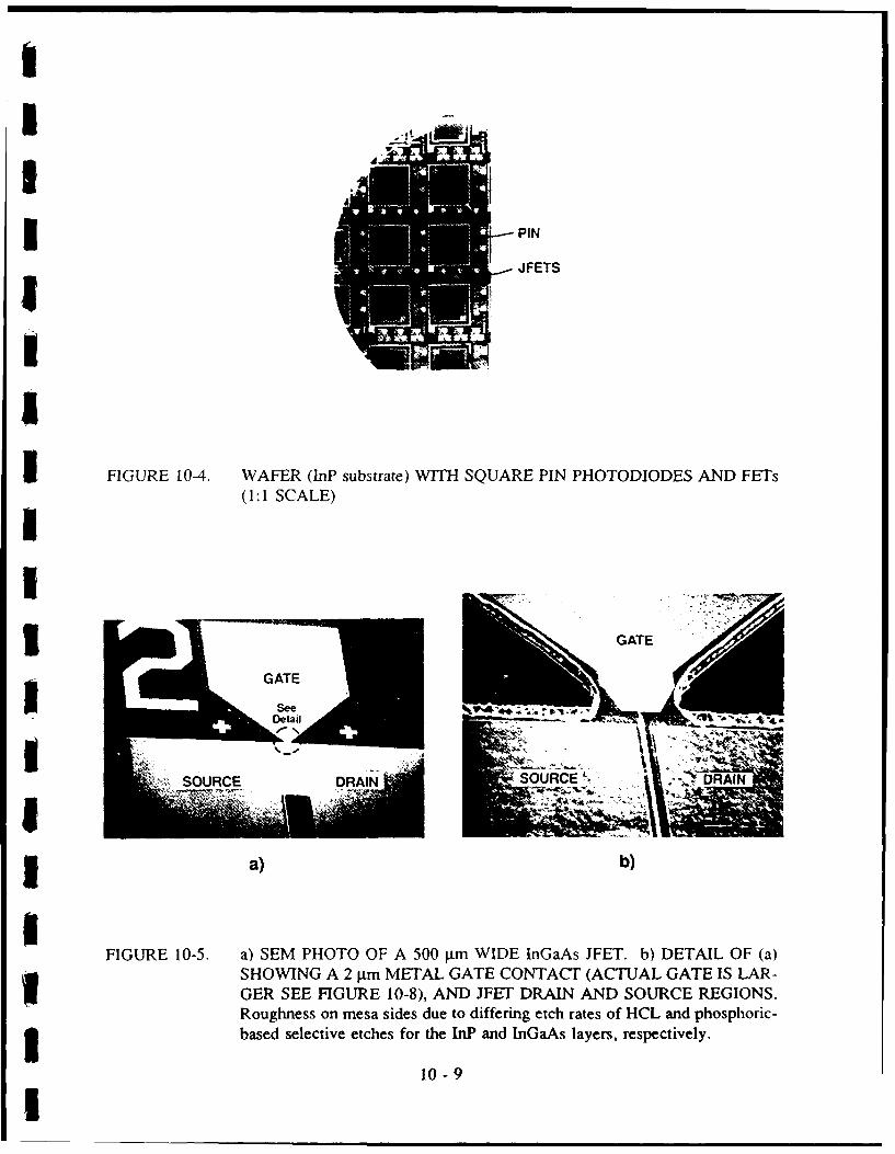
10-5 a) SEM Photo of a 500 pm Wide InGaAs JFET. b) Detailof Showing a 2 grn Metal Gate Contact and JFET Drainand Source Regions .......................................... 10-9
10-6 IV Characteristics of P InP/NInGaAs Gate Heterojunction Diodes ona) InP, b) GaAs, and c) Si Substrates .............................. 10-10
10-7 IV-Curves of InGaAs JFETs with a (P)InP/(N)InGaAs Heterojunction Gateand an (N)InGaAs Channel on an a) InP, b) GaAs, and c) Si Substrate ...... 10-12
10-8 a) SEM Photo of an InGaAs/lnP JFET on a Si Substrate Showing a 2 pinMetal Gate ohmic Contact to a 6 pm P*InP Thin Epilayer ............... 10-13
10-9 Dark and Illuminated IVs of InP/InGaAs/lnP Pin Diodes on a) InP,b) GaAs, and c) Si Substrates, with InGaAs Contact Cap Left on .......... 10-15
10-10 Internal Quantum Efficiency Curve of an InP/InGaAs/InP PIN Photodiodewith InGaAs Contact Cap Left on ................................ 10-17

ILIST OF TABLES
Table Page
8-1 Double-Crystal X-ray Rocking Curve Data for InP Grownwith and without Thermal-Cycle Growth (TCG) on FourDifferent Substrates, Side by Side ................................. 8-4
8-2 Dislocation Density in InP Heteroepitaxial Films,
M easured by Planview TEM ..................................... 8-8
8-3 Minority-Carrier lifetime in InP Layers Measured by PL Decay ........... 8-11
8-4 300 K Hall-Effect Data for 3 tm Thick InP Layers .................... 8-12
8-5 77 K Hall-Effect Data for 3 pm Thick InP Layers ..................... 8-12
10-1 Etching of Lattice-Matched InGaAs and InP (25°C, No Agitation) ......... 10-4
10-2 Comparison of MOCVD Target, Dektak/Etch, and Optical Reflectance ...... 10-5
I 10-3 IV Data of P*InP/NInGaAs Heterojunctions on InP, GaAs and Si .......... 10-11
10-4 Measured InGaAs JFET Transductance and Source Drain Resistance ........ 10-12
i 10-5 IV Data on InP/InGaAs/InP PINs on InP, GaAs and Si Substrate ........... 10-15
IIIIi!iI

I
ISECTION 1
INTRODUCTIONIThe on-chip integration of photonic and electronic devices would facilitate improvements
in high-speed signal processing and lead to rapid progress in the state of the art of electronicsystems. Figure 1-1 shows the concept of such an optoelectronic integrated circuit (OEIC) usedfor high-speed signal processing. These objectives necessitate advances in the field of semi-conductor materials; one promising are that has seen much recent growth is the heteroepitaxy ofIII-V semiconductors on Si substrates. A variety of GaAs-on-Si devices are now being realizedin many research and development laboratories worldwide. Less work has been devoted to thegrowth of !nP on Si despite the importance of InP as an excellent choice for many applicationsin the realn of IR lasers and high-speed/high-power transistors. Our program to develop InP-on-Si structures is based on the extensive foundation of teclmology developed by us and others inthe fields of heteroepitaxy on Si and growth of hP.
Monolithically integrateoptoelectronic I/O devices
/7 optimized for optical
I GanPs transmission- nGalnAs
InP -0 F Advanced high-speed
GaAs IC signal processing
I Low cost
U Large area•High thermal
Si Substrate or Circuit conductivity
- Good strengthI 9Mature processtechnninny91428
I!
i FIGURE 1-1. SCHEMATIC REPRESENTATION OF AN OPTOELECTRONIC INTEGRA-TED CIRCUIT ENVISIONED AS AN APPLICATION OF THIS RE-SEARCH.
I

I
IThe technical approach of this program is the deposition of thin-film InP and InP-In.Ga,.,As dev',. structures heteroepitaxially onto Si substrates by the metalorganic chemicalvapor deno" ,on technique. The use of a GaAs intermediate buffer lzyer has been found inPhase I io be of great utility in achieving high-quality InP layers, and also allows for theintegration of InP and GaAs devices on a largz-area, low-cost, mechanically superior Si wafer.In Phase H we have seen dramatic improvements in the quality of InP layers on GaAs/Sisubstrates by the use of a thermal-cycle growth (TCG) method, in which layer thickness is builtup by a repetitive deposition-anneal-cooldown procedure. The approach of studying the InP-GaAs-Si structure makes use of our well-developed GaAs-on-Si growth process, and provides anintermediate step to help accommodate the 8% lattice mismatch between Si and InP.
The Phase H R&D program described here has shown encouraging progress, which maylead to a technology which has several important benefits. One is to replace the InP bulksubstrates, which are fragile, of low thermal conductivity, available only in small diameters, andquite expensive, with Si substrates which have advantages in all the aforementioned categories.Another is to enable integrated circuits (of Si or GaAs) to communicate optically with otherchips, using silica fiber optics, instead of electrically, via wire data busses. This important newcapability would "harden" the system and aid in its survivability by eliminating interferencepickup on the data bus from hostile jamming and/or electromagnetic pulse effects from nuclearexplosions. Lasers and LED sources and photodetectors, sensitive at the 1.5 .inI attenuationminimum will allow large interconnect lengths and high data rates, while the monolithicintegration of these detectors and sources, made possible by the use of heteroepitaxial structures.will simultaneously utilize the advdnced expertise available in processing and designing logiccircuitry.
II
I
1
I1-2i

Ii SECTION 2
BASIC GOALS OF THE PHASE II PROGRAMIThe basic tasks of the Phase I effort were as follows:
Improvement of the material quality of InP on Si.
3 • Characterization of heteroepitaxial InP films.
Development of a growth process for high-quality, lattice-matchedInhGa,-,As on InP.
Characterization of lattice-matched InrGa,-,As layers.
* Fabrication and testing of PIN and JFET devices, using the Inr.Ga,-XAs-InP-GaAs-Si structures here.
All tasks were successfully completed.
2IU
IUI
I
2-1
U

SECTION 3
OVERALL PROGRAM SUMMARY
The accomplishments of this program are summarized briefly below:
3.1 SUMMARY OF PHASE I
Listed below is a brief summary of the results achieved during our Phase I program:
High-quality single-srystal InP films were deposited on Si substrates by theuse of a GaAs intemediate layer.
InP films were deposited directly onto Si substrates under a variety ofnucleation conditions, but all films were polycrystalline.
Surface morphologies of the best InP-on GaAs-on Si films werespectacular and comparable to GaAs-on-Si films.
Double-crystal X-ray rocking curve analysis showed that the InP qualityimproves with increasing InP thickness, but is fairly insensitive to GaAsthickness.
InP homoepitaxial films grown in this program show state-of-the-art crystalquality.
Analysis by planview TEM shows that InP layers on GaAs-on-Si substrateshave %108 defects/cm 2 , while InP-on-Si samples are polycrystalline.
The InP-GaAs interface appears to generate as many dislocations as doesthe GaAs-Si interface.
InP-GaAs-Si samples showed reasonably good photoluminescence at roomtemperature and 4 K, and that the PL full width half maximum at 300 Kis fairly insensitive to the GaAs buffer thickness.
3.2 SUMMARY OF PHASE II ACCOMPLISHMENTS
Developed annealing techniques for InP on Si (up to 8750, no surfacedegradation, no PH,)
Improved InP on Si by TCG
3-1

Characterized InP on Si ( and on GaAs and GaAs on Si ) samples: byTEM, X-ray, PL, Surface, I-V-T, DLTS, minority-carrier lifetime measure-ments, Hall, and Polaron. Xray FWHM=179 sec, Rt(77 K)=23000cm2/V-sec
Developed growth of lattice-matched In.,Ga,.XAs on InP
Des; ned JFETs and PINs device structures for InMGa,.,As-InP (on TnP,GaAs, and GaAs-on-Si substrates)
Developed fabrication process for PINs and ETs on InP, GaAs, andGaAs-on-Si substrates.
Calibrated growth of PINs and JFETs on InP, GaAs, and GaAs-on-Si
substrates.
* Grew, fabricated, and tested PINs and JFETs on InP, GaAs, and GaAs-on-Si substrates.
I
3-

SECTION 4
PROGRAM ORGANIZATION
The program was directed by Stanley M. Vernon of Spire Corporation, which performedall MOCVD growths and annealing, all device fabrication and testing, and much of the materialcharacterization. Several outside collaborations were utilized to help characterize the structures.Profs. W.A. Anderson and C.R. Wie of SUNY at Buffalo performed double-crystal X-ray rockingcurve analysis, DLTS, and diode measurements during the first year of the Phase II. Low-temperature photolurninescence was carried out at UCLA by Dr. N.M. Haegel andMr. V.P. Mazzi, and transmission electron microscopy was provided by Dr. M.M. Al-Jassimn ofthe Solar Energy Research Institute, Golden CO.
4IiIIIII
1 4-1

I
1SECTION 5
TECHNICAL APPROACHI5.1 FILM GROWTH
IAll films wre grown by atmospheric-pressure MOCVD in a Spire builtSPI-MO CVD 450TM. InP films were deposited onto InP, GaAs, and GaAs-on-Si substrates ina side-by-side fashion using the "450" reactor, which has a capacity of five two-inch-diameterwafers per run. The GaAs-on-Si substrates were formed previously in a separate growth runusing the "two-step" method.(') This procedure basically consists of a high-temperature bakeout(at =1000'C), a low-temperature nucleation step (at = 400'C), and film growth at = 7000 C.Some of the GaAs-on-Si substrates were also treated with a thermal-cycle growth (TCG)process,(" which consists of deposition at 700'C of about 2000A of GaAs, annealing at = 9000C,cooldown to room temperature, and repetition of these steps about five times. For the growthof some InP samples, TCG of InP was performed in a manner analogous to that used for GaAs.
5.2 MATERIAL CHARACTERIZATION
The films grown in this program, including InP layers on InP, GaAs, and GaAs-on-Sisubstrates, have been characterized by numerous techniques, as shown below.
5.2.1 Physical Properties
The three techniques used to study the physical structure of the samples are:
0 Nomarski interference-contrast microscopy. This is performed at Spire andused on a run-by-run basis to examine the surface morphology of thefilms, at magnifications up to 1000X.
0 Double-crystal X-ray rocking curve analysis. This technique is used toassess the structural perfection of the various layers, as well as todetermine the alloy composition of ternary (In Ga.As) layers, with a highdegree of precision. During the first year of the program, the X-raymeasurements were performed at SUNY at Buffalo; at the start of thesecond year, Spire set up its own high-resolution diffractometer, and themeasurements have been carried out in house since then.
Transmission electron microscopy. This powerful technique is used toimage the defect structure of the samples, at magnifications up to severalhundred thousand times. Structures can be examined in cross-section, toreveal the details of the propagation of the defects, or in plan-view, toaccurately determine the defect density over a large area.
5I5-1
I

5.2.2 Electrical Properties
The samples have been studied in terms of electronic transport properties, by thesemethods:
* Hall effect. Performed at Spire, at both 300 and 77 K, to measuremajority-carrier mobility and net carrier concentration.
S Deep-level transient spectroscopy. Performed at SUNY at Buffalo, thisanalysis is used to indentify and quantify the deep-level traps present inthe various structures.
Electrochemical C-V profiling. This technique, commonly called the"Polaron," measures carrier-concentration versus depth, by combining etchand a C-V analysis techniques in an automated fashion.
5.2.3 Optical Properties
Photoluminescence. This method of studing the optical properties of thefilm reveals details about the stress present in the layer, as well as theimpurities, and optically active defects present. Analysis was carried outat 4 K at UCLA.
Photoluminescence decay, with time-resolved photon counting-") Thismethod, which looks at the transient response of the carriers in a crystalto a pulse of light, is used to accurately determine the minority-carrierlifetime of the semiconductor, as well as the surface recombinationvelocity.
I
III
1 5-2

SECTION 6
THERMAL-CYCLE GROWTH OF InP ON GaAs AND Si
The first experiments performed in Phase II were to learn how to grow the best qualityInP on Si possible (i.e., to minimize dislocation density).
The first step was to determine experimentally the minimum PH 3 overpressure to preventthe InP from dissociating in the reactor at the anneal temperature (time held at anneal temperaturewas 30 min.). Temperatures up to 850'C were studied. The results of this trial were determinedby careful Nomarski interference-contrast microscopy examination of the surface of InP on InP,GaAs, and GaAs-on-Si substrates (to check for surface degradation (loss of P)), Hallmeasurements, and room temperature photoluminescence (PL). The PH3 partial pressures werevaried between 7.5 torr and 56 torr. It was found that a maximum temperature of 800'C couldbe used with a PH 3 flow of 80 sccm, and a main H2 flow of 1.0 sLPM, resulting in a PH 3 partialpressure of 56 torr.
Next, experiments with the TCG of InP were done using GaAs substrates. After a processwas worked out, it was then easily transferred to GaAs-on-Si substrates. The optimum numberof cycles (three), and thickness per cycle (I [tm) were set from past experience with the thermal-cycle growth (TCG) of GaAs on Si.12' The test structure studied is shown in Figure 6-1.
I
CONVENTIONAL Growth TCG
at 600"800"800"
3 nm InP800"
600* Grown - lj-- im InP ------ 800'
i Substrate Substrate
IFIGURE 6-1. InP HETEROEPITAXIAL STRUCTURES STUDIED DURING THESE
EXPERIMENTS.
6-1I

Further trials revaled that actually we could go to an arnealing temperature as high as875 0C for the TCG process without InP-surface degradation, and using the same partial pressureof PH,. A number of samples were grown by this new TCG process and characterized. Muchto our disappointment, these samples did not show any improvement over the films grown withthe 8000C TCG process. It seems as if the nature of InP is such that the defects cannot be5m annealed out as easily as in GaAs, where the TCG process has been much more successful.Recently, it has been shown that a graded layer of InGa ,As (x graded from 0 to 0.53) iseffective at reducing the dislocation density in InP on GaAs/Si films, 4 and this is the avenuewhich we will be pursuing in the future.
6
m
IU
I
I
I -m

3 SECTION 7
THERMAL-CYCLE ANNEALING (TCA)
_ OF In.Ga1 1 As-InP STRUCTURES ON InP,
GaAs, AND GaAs-on-Si SUBSTRATESI
Another alternative process was developed in order to minimize the use of pyrophoric PH,in large quantities during the TCG process. This new process involved the use of a lattice-matched capping layer of InGa,-,As, and annealing under an AsH 3 overpressure. Annealingtemperatures as high as 9000C were achieved, but most samples studied used an annealtemperature of 875'C. Two alternative processes were developed: One method consisted ofannealing the In Ga 1.,As-capped InP, with the wafer in the nomal "face-up" position. The wafersurface would severely degrade, due to the loss of In from the InGa1.As; but the underlying Iml;3 would not be harmed. A selective etch would be used to remove the top layer (In.Ga1,_As), andthus revealing the annealed InP film. Another recipe would involve a similar annealing of anl nGa_,As-capped InP film, with the wafer placed "face-down" on the susceptor. This served to3 "seal" the InrGa,. As and prevent In loss from the surface, thus eliminating the need for theselective-etch step. Both variations of the TCA method gave similar defect density results;however, neither was superior to the best results achieved with our TCG process, even thoughthe maximum annealing temperature was 75°C higher. This is due to the fact that TCA is notas effective at reducing the dislocation density as is the TCG process. This has been seenpreviously for the case of GaAs on Si. unfortunately, it is also true for InP on Si. The TCAIexperiments and results are described in more detail in Appendix B.
7U
I
U
7-1
,,IIi

U* SECTION 8
RESULTS OF InP THERMAL-CYCLE GROWTH (TCG) EXPERIMENTS ON
InP, GaAs, AND GaAs-on-Si SUBSTRATES.
A number of samples of InP, deposited by thermal-cycle growth (TCG), were analyzedI by numerous characterization techniques and compared to others deposited by conventionalgrowth; the data are presented and discussed in the following sections:
Figure 8-1 is schematic representation of the thermal-cycle growth process used through-out these experinents. Figure 8-2 shows the details of time-temperature shedule used for the3 TCG process. For InP, the anneal temperature is 800'C, the growth temperature is 600', and theamnbient contains 56 torr of PH3; for GaAs TCG, the anneal temperature is 950'C, the growth isdone at 700' , and the ambient contains 36 tort of AsH 3.
U
I InP 2 gm
InP 1 jamGrowth anneal 800", 20 min.at 600" " I cool to 250"
U nP 1Mpm
______ I gmanneal 950', 2 min.cool to 250'
I GaAs wafer12" off (100) co (111)]
SUBSTRATES
andGaAs (1. m)
on Silicon[2" off (100) * (111)]
91429
FIGURE 8-1. SCHEMATIC REPRESENTATION OF THE InP THERMAL-CYCLEGROWT- (TCG) PROCESS.
8-1
U

I
cc300,-I
0 2 3 4
TIME (hours)
I!w
iFIGURE 8-2. TEME-TEMPERATURE CYCLE USED FOR THE THERMAL-CYCLE
GROWTH (TCG) PROCESS.
i 8.1I PHYSICAL PROPERTIES
IThe surface morphologies of InP deposited on GaAs by the two different processes are
shown in Figure 8-3. The TCG sample has a much smoother morphology. This correlates tothe lower density of stacking faults present in the layer; stacking faults, which are fairly easy to
I remove by annealing, (5) often cause fairly rough surface features to appear. The morphology of
InP-on-GaAs-on-Si samples are quite similar to those of InP on GaAs.
I A double-crystal X-ray rocking curve of InP-on-GaAs-on-Si is shown in Figure 8-4, with
a more detailed scan of the lnP layer shown in Figure 8-5. The sample studied here was not
annealed. The best values obtained for the full width half maximum values are listed inI Table 8-1.
300-2
II • ,I

* lnP-TCG in P-No Anneal
r til
InP
Si
i--l
FIGURE 8-4. TYPIALK DOULCRYSAL OFRAYOCNG GRWN WITH ANDP
GasS SAMLE
8 -

I FWHM = 301 atc-seconds
Gaussian fit Power
800
700
3,600500
.1 400
0II 6 300200
100
31.4 31.5 31.6 31.7 31.8 31.93 Theta (degrees)
FIGURE 8-5. DETAIL OF THE ROCKING-CURVE PEAK FOR THE InP LAYER OF3AN InP-GaAs-Si SAMPLE.
TABLE 8-1. DOUBLE-CRYSTAL X-RAY ROCKING CURVE DATA FOR lnP GROWNWITH AND WITHOUT THERMAL-CYCLE GROWTH (TCG) ON FOURDIFFERENT SUBSTRATES, SIDE BY SIDE.
I SUBSTRATES FWHM (arc-sec)3 InP TCG InP
InP 15 15GaAs 236 179
GaAs/Si 340 273TCG GaAs/Si 286 194U
Note: In all samples, InP layer = 3 gim thick, and GaAs layer - 2 gm thick; the TCG process5 for the GaAs-on-Si growth involved 3 cycles at 950*C.
Im 8-4
I i II

I
I The trends evident here are that TCG InP is better than unannealed InP, and that TCGGaAs/Si substrates are better (for the growth of InP) than standard GaAs/Si, and are almost3 comparable in quality to bulk GaAs wafers.
Figure 8-6 shows a planview TEM comparison of regular InP and TCG InP, each grownon TCG GaAs/Si substrates. The TCG InP process resulted in a reduction in dislocation densityof only approxinately a factor of three. Sinilar comparisons in the GaAs-on-Si studies show thatTCG is much more effective; Figure 8-7 shows a typical comparison of GaAs on Si versus TCG3 GaAs on Si, where the dislocation density has been reduced by a factor of twenty.
InP-TCG
...
I
3 InP-No Anneal
II
I
FIGURE 8-6. PLANVIEW TEM MICROGRAPHS OF InP-GaAs-Si SAMPLES, GROWN3I WITH AND WrIHOUT THE InP TCG PROCESS.
8-5

No Anneal with TCG
I
,/ .~PHOTO-MONTAGE
LINE
GaAs-Si -
INTERFACE -. w m alim
4X 10 "cm2 2X10 7 CM-2
FIGURE 8-7. CROSS-SECTIONAL TRANSMISSION ELECTRON MICROGRAPHS OFGaAs on Si GROWN WITH AND WITHOUT TCG OF GaAs.
3 Figure 8-8 shows cross-sectional transmission electrogi micrograph of an InP/GaAs/Sisample, the defects in the InP are seen to originate mostly at the GaAs-InP interface, due to the4% lattice mismatch present, with only a few of the InP defects coming from those in the GaAswhich propagate through. This explains why the quality of the InP layer is only weaklydependent on the quality of the GaAs layer on Si.
A high-resolution lattice-imaging micrograph of an InP-on-GaAs sample is shown inFigure 8-9. A uniformly-spaced array of misfit dislocations is seen at the interface, with an3average spacing of -100, as expected from the mismatch between GaAs and InP.
The best results obtained for InP on GaAs, and on TCG GaAs/Si are shown in Table 8-2.3 Also included are the results for the TCA process discussed in Section 7.
We also tried to reduce the dislocation density in the InP by the use of a strained layer
of 1000A of In,1Gal, As, with x = 0.65, corresponding to a strain of = 1.0%. A cross-sectionaltransmission electron micrograph of this structure is displayed in Figure 8-10. Unfortunately, thissamnple had a dislocation density as high as similar samples without the hInGa,.As layer. CloserTEM study of this sample revealed many defects originating at the InP-InGa, 1As boundary, dueto a growth problem which led to a poor interface.
I8-6I

In
GaI
Si~ 05pm
FIGURE 8-8. CROSS-SECTIONAL TRANSMISSION ELECTRON MICROGRAPH OFInP-GaAs-Si GROWN WITHOUT TCG.
/r /7 //§'.
Io
GaI
I FIGURE 8-9. HIGH-RESOLUTION LATTICE-IMAGING TEM MICROGRAPH (CROSSSECTION) OF THE InP-GaAs INTERFACE, SHOWING AN ARRAY OFMISFIT DISLOCATIONS.
8- 7

5TABLE 8-2. DISLOCATION DENSITY IN hIP HETEROEPITAXILAL FILMS,MEASURED BY PLANVIEW TEM.
STRUCTUJRE DEFECTS PER CM2
I ________ On GaAs On GaAs/Si
InP 3.9 x 10" 3.0 x 10"TCA - InP 1.9 x lol 2.0 x 10"
TCG -InP 6.0Ox 10, 9.0Ox 10'
In
In
-8

II
8.2 OPTICAL PROPERTIES
3 Figure 8-11 shows the low-temperature photoluminescence (PL) data for InP grown onGaAs, and on TCG GaAs/Si substrates; Figure 8-12 shows similar data for InP grown by theTCG process. A comparison of the two reveals a number of features indicating that the TCG InPis superior material. The ratio of the exciton peak to the band-to-acceptor peak indicates a higherminority-carrier lifetime (t) in the annealed samples. The fact that the exciton peaks on the TCGInP sample are higher and narrower are also indicative of the material quality. The wavelengthshift of the exciton peak of InP on InP compared to InP on GaAs (shift toward higher energy)is due to the fact that hnP on GaAs is in compression; for InP on GaAs on Si the shift is towardlower energy (hiP is in tension), since this structure is dominated by the thennal coefficient ofexpansion of the Si substrate. In Figure 8-11 we note that the PL from haP on bulk GaAs andon TCG GaAs/Si are similar in shape, again showing that these two substrates usually yield
I similar results for InP growth.
X10C0
3 50-
4.5 - xioI Band To Acceptor Peak
I i 4.0
3.5I Ga'
.3.0i Ga" I200
" 2 2.5
2. 0lo x It
i 1.6 ZPx
1.0
0.5
I ~ ~~~~~~~~~0.0- Ii i I I I
1.27 1.31 i.35 1.39 1.4,3 1.,47
Photon Energy (eV)
FIGURE 8-I1. 4.2 K PHOTOLUMINESCENCE OF InP ON VARIOUS SUBSTRATES-i CONVENTION GROWTH.
8-9

I
1 5.0 X 700
4.5 Band To AcceptorlExciton PeakPeak I\ (Split
Valance
4.0 1 Band)
3.5
U 3.0Ga.o
I 2.5
2.01., In.P X1
i 1.5-
1.0
1 0.5
0.0 i i I 'i |in , I I , I I1.27 i.31 1' 1.35 1.39 1.43 1.47
Photon Energy (eV)I
I FIGURE 8-12. 4.2 K PHOTOLUMINESCENCE OF InP ON VARIOUS SUBSTRATES-TCG PROCESS.I
The minority-carrier lifetimes of the various structures have been studied by the PL-decaytechnique;"" typical raw data for these measurements are shown in Figure 8-13. The results aresummarized in Table 8-3.
3 These data show that the TCG InP on GaAs or Si has a longer minority-carrier lifetimethan that of unannealed InP on similar substrates. We also note that the exact substrate structuremakes little difference in the lifetime values, while the Inp on InP is an order of magnitudebetter. The absolute lifetime values listed here are all lower that what they would be if themeasurement were not dominated by the surface recombination velocity (SRV) of the InP sur-face; the comparisons among the relative values are still meaningful, however. To overcome theeffect of the surface recombination velocity, we would need an lnP layer which is passivated bya low SRV material, or is very thick (greater than 10 jim). Neither one of these structures was
-- practical for our studies.
i 8- 10

S10 4
InP on InP7 = 3.70 nsec
3 Counts
00 Tinsecd 50
10 4
InP-GaAs-Si(TCG) (TCG)"T- 0.75 nsec
Counts
II0- A A
1o0
00 Tinsecl 50
FIGURE 8-13. PHOTOLUMINESCENCE-DECAY MEASUREMENT OF InP LIFETIMESON InP AND GaAs-on-Si SUBSTRATES.
TABLE 8-3. MINORITY-CARRIER LIFETIME IN InP LAYERS MEASURED BY PLDECAY.
I SUBSTRATES LIFETIME (nanosec)
InP TCG InP
InP 3.7 2.9GaAs 0.415 0.593
GaAs/Si 0.475 0.55TCG GaAs/Si 0.464 0.75
3 Note: Ml InP layers are 3 pm thick, and undoped, with n = 0.4 - 2.0 x 10i' cm-3 .
I3 8-11

U
i 8.3 ELECTRICAL PROPERTIES
Hall-effect measurements were performed, at 300 and at 77 K, on undoped InP layers,3pm thick, grown side by side, on semi-insulating GaAs and InP wafers. Hall measurementscould not be done on samples deposited on Si substrates, due to their high conductivity. The3 data are presented in Tables 8-4 and 8-5.
3 TABLE 8-4. 300 K HALL-EFFECT DATA FOR 3-pm-THICK InP LAYERS.
EPI SUBSTRATE MOBILITY CARRIERS(cm 2/V-sec) (cra3 )
TCG InP GaAs 1,920 9 x 10¹⁴
TCG InP InP 3,180 1.5 x 10¹⁵
3 InP GaAs 1,440 6 x 10¹⁴
InP InP 4,150 6 x 10¹⁴
TABLE 8-5. 77 K HALL-EFFECT DATA FOR 3-pm-THICK InP LAYERS.
EPI SUBSTRATE MOBILITY CARRIERS(cm2/V-sec) (cm -3)
TCG InP GaAs 23,000 4 x 10¹⁴
TCG InP InP 47,200 9 x 10¹⁴
3 InP GaAs 8,700 2 x 10 4
InP InP 72,200 5 x 10 4
IThese data clearly show the beneficial effect that TCG has on the majority transport
properties of InP on GaAs. At 77 K, for unannealed InP, the ratio of the mobilities on GaAs andon InP is only 0.12; for TCG lnP, this ratio increases to 0.49.
A Polaron (electrochemical capacitance versus voltage) profile is displayed in Figure 8-14for a typical InP-on-GaAs-on-Si sample. The high background in the GaAs layer is due to diffu-sion of Si, which is greatly enhanced by the high dislocation density.6) The peak at the InP-GaAs interface reveals how the Si atoms tend to "pile up" at the point of high dislocation density.Thus, this interface acts as a gettering region.
Ii 8-12

I1
I ~ 101
0I:dI
1 6 a ~ s S lic
c
ILIu
12 3 453 DEPTH (Jim)
3 FIGURE 8-14. TYPICAL CARRIER-CONCENTRAT7ON POR PLRN PAInP-GaAs-Si STRUCTURE. RFL PLRN FA
3~ 8-13

I
I SECTION 9
GROWTH OF LATTICED-MATCHED In.Ga,.As ON InPIThe MOCVD growth of In Ga,.1 As latticed matched to InP was developed during the3 Phase II program so that the demonstration devices, PIN photodiodes and JFErs, could be
fabricated in this material at the end of the program. Another use of lattice-matched IrGa,.,Aswas as a caplayer for the TCA process (see Section 7 above); also, lattice-mismatched InGa1 ,As3 layers were used to introduce strain into the structure in an attempt to reduce the dislocationdensity. (See Section 8.1).
The first experiments on InGa,. As growth were carried out at atmospheric pressure,using trimethylindium (TM!) and trimethylgallium (TMG) as the Group M source reagents. Thecompositional unformity was a problem at 760 torr; this had also been noted in past experienceswith the growth of GaAsP, so we quickly adopted a reactor pressoure of 76 torr instead. Anotherproblem noted was that the composition was not very reproducible; this phenomenon has plaguedthe growth of IrqGa1.xAs in many other labs, and is often due to the problem in obtaining areproducible pick-up rate of In vapors from the solid TMI source. Therefore, we began usinga liquid source, ethyldimethylindium (EDMIN) instead. This greatly improved the control overour process, although efforts to improve our composition reproducibility are still continuing, sincefor most critical applications, the specifications on the permissible lattice mismatched are verystrict: i.e., = 400 ppm (= Aa/a).
I The low-pressure growth process quickly yielded excellent results in terms of composi-tional uniformity over a full two-inch-diameter wafer. Figre 9-1 shows the typical uniformitymeasured by double-crystal X-ray rocking curve analysis over the full wafer surface. The bestvalue achieved for uniformity of lattice mismatch over a two-inch wafer is Aa/a = 2.1 x 10- . A-state-of-the-art FWHM of the double-crystal X-ray rocking curve peak of the InGa,.XAs layerof only 18 arcsec has been achieved, with a lattice mismatch of only 27 ppm (= Aa/a) (seeFigure 9-2). These excellent results have been reproduced on several occassions.
Several other combinations of Group II source reagents were used, but with out success.They include trimethylindium and triethylgallium (TEG), and EDMIn and TEG. The vapor pres-sure of TEG is lower than that of TMG, so larger carrier flows of H2 can be used to achieve thesame delivery rate of In; this would improve our chances at reproducibility, since part of theproblem may be due to the inaccuracy of the mass flow controller when forced to operate at thelow end of its range. Although many other laboratories use TEG for the growth of InGa, ,As,3 we were unable to achieve high-quality films. Our problem seems to have been due to a contam-inated TEG source. The decision was made to abandon this line of attack, so all further workwas carried out with TMG and EDMNn.
II9-1I

UI WAFER • .552
* G• .551 A
S
S.545 .550 .549 .543 F550 L
0I wI e .546
* .546 ROTATIO N
Xave = .548Std. Dev. = .0031Uniformity = 2.1 x 10-4 = 0.02%U
FIGURE 9-1. COMPOSITIONAL UNIFORMITY MAP OF LATTICE-MATCHEDU Ir;Ga- As ON InP OVER A TWO-INCH WAFER.
25000
I IFWHM =18.2 arcsec
20000 I Lattice Mismatch2.7 x 10-5
015000
I
M05-1323
00 200 400 600 800 1000 1200 1400 1600
RELATIVE ANGLE (arcsec)
FIGURE 9-2. X-RAY ROCKING CURVE OF LATTICE-MATCHED InGa,1 As ON InP,GROWN BY LOW-PRESSURE MOCVD.
* 9-2

I
I SECTION 10
lnGaAs FIELD EFFECT TRANSISTORS AND PHOTODIODES
10.1 INTRODUCTION
Junction field effect transistors (JFETs) were fabricated in InP/InGaAs epilayers on InP,GaAs, and Si substrates to test the suitability of the heteroepitaxial layers for analog and digitalcircuits. An FET is a good demonstration device since it is a basic building block in both linearand digital ICs. A iunction FET was used, instead of the Schottky-gate MESFET typical ofGaAs ICs, since gate metals form poor Schottky barriers to the low-bandgap Ino.53Ga,.47As(0.75 eV vs. 1.42 eV for GaAs).
In FETs majority carriers dominate the source-to-drain current, unlike minority-carriercontrolled BJTs and HBTs. Majority carrier devices are relatively undisturbed by dislocations andother material defects. At low bias, the net carrier (drift) velocity, which influences speed, maydecrease as the mobility decreases due to carriers scattering off dislocations and other materialdefects. However, most FETs operate with a large bias such that carriers transit the FET channelat their mobility-independent saturation velocity.
The minority carrier lifetime, on the other hand, is extremely sensitive to dislocationdensity, and concentration and capture cross-section of material defects acting as recombinationsites. PIN photodiodes were made to demonstrate minority carrier device operation in thematerial. PINs are key components in integrated photoreceivers, and are ideal test vehicles forSpire, since characterization facilities for quantum efficiency already exist.
10.2 MOCVD EPITAXIAL DEVICE LAYER DESIGN AND GROWTH
I 10.2.1 Junction Field-Effect Transistor (JFET)
Although it is possible to grow a single InP/InGaAs epilayer structure for the monolithicintegration of both a JFET and a photodiode, for this effort we decided to grow separatestructures for each. This enabled us to use optimum dopings and thicknesses for each device,including etch-stop layers so that wet chemical etches would stop at precise depths in the devices,eliminating the need to depend on pre-determined, doping-dependent etch rates during deviceprocessing.
I Figure 10-1 shows the InGaAs/InP JFET layer structure. The top gate layer of P InPforms a P-N heterojunction with the n-In_0 53Ga0.47As channel. The reverse-biased depletion regionof this junction extends mainly into the In0 3Ga0.,,As channel and controls the electron flowbetween source and drain in the JFET.
A P InP/NInGaAs heterojunction was used as the gate junction instead of a P4InGaAs/N"InGaAs homojunction, since any viable manufacturing process will need an etch stop such as anlnGaAs/InP interface between the gate and FET channel layer. The etch stop allows the InP gateto be defined and the source and drain regions cleared of InP by a selective etch in a
3 10- 1

I
I Gate Layer InP 0.2 gm P = 1E18
Channel InGaAs 0.3 p.m N= E i7
3 Buffer InP 1.5m P = 5E16
3 Buffer InP 0.5 pm P - 1E19
InP-TCG Buffer 3 gm InP-TCG Buffer 3 p.mInP P - 1E19 P - 1E19
S.I.Substrate GaAs GaAs 1 lam
S.I.Substrate Silicon Substrate
91430
3 FIGURE 10-1. DESIGN OF THE EPITAXIAL LAYERS FOR THE JFET STRUCTURE.
I reproducible manner, without the worry of etching through the thin FET InGaAs channel.Because the top PInP gate layer has a much different chemistry than the Inh0 53Gao.47As nchannel,it should be possible to find a selective etch for the InP that will automatically stop at theIn., Gao.47As FET channel. This is a very important feature, since if a timed etch is used witha PInGaAs/NInGaAs homojunction instead of a selective etch utilizing the InGaAs/InP hetero-junction, it would be easy (and disastrous) to accidently etch through the relatively thin
In0 . 3Ga 0.47As channel region, since there is nothing to automatically stop the etch at the righti point.
The "zero-bias" depletion region between the P InP buffer and the heavier doped n-
Ino.53Ga., 7As channel extends mainly into the P InP and helps to isolate the JFET channel fromthe conducting TCG-InP layers used in the growths on GaAs and Si substrates.
The doping N, (101 7/cm 3 ) and thickness "a" (0.3 prM) of the Ino.53Gao.47As JFET channelin Figure 10-1 were selected to obtain good FET performance at a reasonable pinch-off voltageVp, qNta 2/2, about 6 volts. The top P+InP needs a high doping for a good ohmic contact, as wellas to insure that most of the depletion region extends into the N InGaAs FET channel. Thislayer should be thick enough so that the gate ohmic contact to the top InP does not alloy throughand short out the junction. The bottom P- InP layer should be lightly doped compared to thechannel region, so that its uncontrolled depletion region does not extend into the FET channel.The exact thicknesses and dopings of the InP regions, unlike that of the InGaAs channel, are notcritical.
U3 10-_2

I
1 10.2.2 PIN Photodiodes
Figure 10-2 shows the structure of the PIN photodiode. The top N' InP layer (1.34 eV)acts as a window which allows light above 930 run to transit through with little absorption, whilepreventing, through favorable alignment of the energy bands, minority carriers generated in the
0.75 eV In0.53Gao47As "intrinsic" region from recombining at the front surface of the wafer. Thewindow allows light from 930 nm to the Ino.s5 Ga0.47As absorption edge of 1650 nm to passthrough relatively unimpeded. The exact window thickness is unimportant, except it should bethick enough so that the top CrAu contact, when annealed, does not alloy through this layer andshort out the diode. It should be heavily doped in order to make a good ohmic contact.
I
Cap InGaAs 0.13 itm N = 1E19
Window InP 0.75 p.m N = 1E18UI Layer InGaAs 4 .m N = 3E15IBuffer InP 0.5 .tm P - 1E19
InP-TCG Buffer 3 .m InP-TCG Buffer 3 .mInP P - 1E19 P - 1E19S.I.
Substrate GaAs GaAs 1 p.mS.I.
Substrai .... C,,strateg1431
U3 FIGURE 10-2. DESIGN OF THE EPITAXIAL LAYERS FOR THE PIN STRUCTURE.
iThe intrinsic region should be doped as lightly as possible for maximum depletion width.The length of the intrinsic region 'i' is a tradeoff between several factors. Concerning quantumefficiency, "i" should be at least several absorption lengths, and yet thin enough for the junctionto deplete through, to insure efficient carrier collection. Concerning speed, "i" should be thickto minimize the device capacitance, yet thin enough so that the carrier transit times do not slowthe photodiode. Concerning noise, "i" should be thin to minimize the space-charge generation-recombination currents, which is proportional to the depletion region volume.
10-3

IOne absorption length for the Ino.53Ga0 47As is about 1 Rm, so 3 Jim allows for about 95%
of the light to be absorbed. Assuming an undoped "intrinsic" background of 10"5/cm 3, the zero-bias depletion width should be 0.9 pm. At 5 volts of reverse bias, the entire 3 Kn intrinsicregion should be depleted. The capacitance of the diode at -5 volts reverse bias should be3.8nF/cm2 . Assuming a 50 ohm load, the RC time constant for a I cm2 device is 190 ns. Thecarrier transit time is roughly the saturation velocity over the length of the depleted intrinsicregion (3 pam), or about 30 ps. Therefore, the speed of this very large area detector iscapacitance limited, and we would like to make the depletion region as large as possible.However, with the current background doping of lO 5 /cm 3, 3 Krm is about all that can be depletedat modest reverse bias voltages. Therefore, 3 pm was chosen as a good target thickness for theintrinsic region, along with whatever minimum background doping that could be achieved, whichwas assumed in the above calculations as 1015/cm - .
10.3 DEVICE PROCESSING
5 10.3.1 Etch Characterization
In order to make contact to the various buried epilayers of InGaAs and InP in the devicestructures, it was necessary to find selective etches which would etch InGaAs but not InP, andvice versa. Table 10-1 gives some wet chemical etch rates for some common etchants on InP
5 and InGaAs.
TABLE 10-1. ETCHING OF LATCE-MATCHED InGaAs AND InP (25°C, NOAGITATION).
ETCH MATERIAL RATE COMMENTS(ptm/min)
HCL N InP 9.5 Smooth; rate linear w/timeSi InP 10.5 Smooth surfaceP InP 8.9 Rough surface3 N InGaAs 0.04 Smooth, surface
IHCL: IDI Si InP 0.15 Smooth surfaceP InP 0.53 Rough surface;not linear w/time
N InGaAs 0.00 Smooth; no etching after 5 min.
IHCL:3DI Si InP 0.00 No etching1H.PO4 :1H 20 2:8D1I InP 0.00 No etching
*Conclusions:
* HCL etches all InP at 10 grm/min. and slows at InGaAs to 400A/min.* 1:1:8 selectively etches InGaAs but not InP. We know it etches InGaAs
from previous work at Comell and Spire.IDI:IHCL selectively etches InP (doping depend.) but not InGaAs.
I10 - 4I

I
IThe above data in Table 10-1 were taken on bulk InP or a thick InGaAs epilayer. Sinceselective etching is critical to the program's success, and because we wished to confirm that thetarget MOCVD epilayer thicknesses were accurate, a second experiment on an actual PIN diodewafer piece from lot 1274 (Figure 10-2) was performed. The selective etches determined fromTable 10-1 were used to alternately selectively etch away InGaAs and InP layers. Each etch step
Swas measured by DEKTAK surface profiling to gauge that particular layers thickness. Thismethod of confirming the thicknesses of the MOCVD epilayers is destructive. In addition, beforethe etching and DEKTAK measurements, the optical reflectance of the PIN layer on InP wasmeasured. This reflectance data was fit using a Spire-developed optical reflectance modelingprogram known as REFIT (REflectance FITting). This optical method, which is non-destructiveand quicker, is preferred when accurate optical data files for the material is available.
Thicknesses of a nominally lattice-matched InGaAs/InP NIP photodiode layer on an InPsubstrate measured by selective etching/Dektak, and by optical reflectance, are compared to theMOCVD target structure in Table 10-2. Figure 10-3 shows the measured optical reflectance ofthe PIN structure (heavy dots) and the theoretical fit (solid line).ITABLE 10-2. COMPARISON OF MOCVD TARGET, DEKTAK/ETCH. AND OPTICAL
REFLECTANCE. Thickness of InGaAs and InP layers in PIN structure ofFigure 10-2.
Target Layer Selective Etch Opticaland Dektak Reflectance
(REFIT)
1300k InGaAs 1000k 930A7500k InP 3300, 3700A4 gm InGaAs 3 .un 3.2 .n5000A InPg S.I. InP
Comments:
1 1. The InGaAs reflectance data used is from Reference 7.
2. The reflectance fit from 800 to 1800 nm between the measured data and the theoreticaldata was not as good a fit as is common for GaAs-based or Si/SiO2 structures. Theoptical data files need improvement. However, the agreement with the etch/dektakdata indicatcs that even with the current data files, the thickness determined byreflectance is accurate to within about 15%.
3. The selective etch used for InGaAs was 1H3PO4:1H 20 2:8DI (0.24 gn/rnin). It stoppedat the InP.
10-5

0.e
.9
1 .5+) 5
.4
c 4. % i
I1Z
Wavelength (nm)IFIGURE 10-3. COMPARISON OF MEASURED OPTICAL REFLECTANCE OF PIN
STRUCTURE OF FIGURE 10-2 WITH THEORETICAL REFLECTANCEFIT USING DATA FROM NEE AND GREEN. 7
4. The selective etch used for InP is IHCL:IDI (0.4-1 grnm/min). It stopped at the InGaAs.
1 5. A definite visual color change can be seen on the wafer as the InP or InGaAs materialis cleared by the etch. This is convenient in determining that all material (either InP orInGaAs) is etched away. This color change is due to the large index of refractionp difference between InGaAs and InP. However, for very thin layers, it is more difficultto observe.
- 6. The InGaAs growth rate seems to be consistently about 30% lower and the InP growthrate also seems to be about 50% less than what was expected for this run (M05-1274).
I10.3.2 Process Sequence for Devices
Below is an abbreviated description of the process sequence used to fabricate both theJFETs and PINs. The devices are quite amenable to monolithic integration, since similar metalli-zation and isolation processes are used for both devices. The final devices fabricated for this
program were done in two different epilayer structures, however, to optimize the results.
S1. ID wafer backs with MOCVD run #1274-1(PINs) & 1275-1 (FETs)
2. Cleave off a small piece of 1274-1 and 1275-1 and save in labeled envelopes for etch
calibration
10-6

I
3. Clean wafer fronts well with de-ionized water (DI)
4. Spin AZ1375 photoresist at 4000RPM on wafer fronts for mesa isolation
5. Bake photoresist 90'C for 30 min.
1 6. Expose through positive photomask INGAS 1-MESA
i 7. Develop
8. Postbake resist to harden for 90'C 30 main.
i 9. Wafers 1274 ONLY! Use 1H3P0 4:lH20 2 :8DI to etch InGaAs cap- about 25s Is colorchange seen?Use 1DI:IHCL to etch N InP - about 20sIIs color change seen?Use 1:1:8 to etch intrinsic InGaAs - about 6 min.5 This etch stops at bottom InP surface (for back PIN contact)
10. Wafers 1275 ONLY! Use 1:1 to etch P+ InP for about I min. Should see color changeat InGaAs etch stop due to difference in refractive index of InGaAs and InP Use 1:1:8I to etch N InGaAs - about 1 minColor change?Use 1:1 to etch P InP - about 4 minNo etch stop, should be no color change.This etches deep into substrate, isolates the FETs.
11. Photosteps for metal to P+InP (FET gate, PIN back contact) Reverse Image Both 1274
and 1275 Spin AZ1375 4000RPM
1 12. Bake 90'C for 30 min.
13. Expose through positive photomask INGAS1-GATES
14. Ammonia Bake for image reversal
15. Flood expose to UV source for image reversal
16. Develop
I 17. Evaporate fronts of all wafers with 2000A AuZn
18. Liftoff metal covered photoresist in 30 minute acetone soak and spray, leaving metal fortop gate FET contacts and top PIN contacts
19. Sinter 1274 wafer only 6 min. 400'C in forming gas (FG) Purge=cool=10 min. in FG
I10 - 7I

I3 20. Sinter 1275s Only 4 min. 275'C in FG
Purge=cool=10 mmn. FG(shorter cooler sinter out to avoid damage to gate junction)
21. Check contacts
3 22. Photosteps for metal to etched surface (source/drain contacts to InGaAs for FETs, topcontact to InP for PINs)Reverse Image on Both 1274 and 1275Spin AZ1375 4000RPM
23. Bake 90'C for 30 min.
24. Expose through positive photomask INGAS1-OHMICS
i 25. Ammonia Bake for image reversal
26. Flood expose to UV for image reversal
27. Develop
1 28. Wafers 1275 only! Etch away top P+InP in 1:1 to InGaAs etch stop Use Calibrationsample first to get etch time to color change, then all 1275 wafers for same time
I (This etches InP from source/drain FET areas, revealing InGaAs)
29. Microscope inspection
30. Evaporate all wafers with 400A Cr,then 3000A Au
31. Wafers 1274 ONLY! Etch calibration in 1:1:8 to color change
Then all 1274 wafers to color change in about same time! This step etches InGaAs contact cap off window area of PINs.
For this work, one substrate (InP, GaAs and Si) of each layer type (JFET, Figure 10-1 andPIN, Figure 10-2) was available for process development and final devices (six wafers in total).IA typical processed wafer piece is shown in Figure 10-4.
10.4 ANALYSIS AND DISCUSSION OF DEVICE RESULTS
10.4.1 InP/fnGaAs/fnP Junction Field-Effect Transistors (JFETs)
The JFETs fabricated are seen in Figure 10-5. Successful JFETs were made in lattice-matched InGaAs on InP and lattice-mismatched InGaAs-on-GaAs substrates. JFETs on Sioperated poorly. We believe this is due to a larger leakage current in the FET gate (P)InP/(N)InGaAs junctions on the Si substrate.
110 - 8I
3 PIN
JFETS
IFIGURE 10-4. WAFER (InP substrate) WITH SQUARE PIN PHOTODIODES AND FETs(1: 1 SCALE)
GAT GATE
SSOURCE DRAIN 'SURCE DRAI
FIGURE 10-5. a) SEM PHOTO OF A 500 jim WIDE LnGaAs JFET. b) DETAIL OF (a)SHOWING A 2 tim METAL GATE CONTACT (ACTUAL GATE IS LAR-GER SEE FIGURE 10-8), AND JFET DRAIN AND SOURCE REGIONS.Roughness on mesa sides due to differing etch rates of HCL and phosphoric-3 based selective etches for the Iii' and InGaAs layers, respectively.
10 -9

I Figure 10-6 shows IV curves of relatively large area P+InP/NInGaAs heterojunctiondiodes on the three material substrates. Because of the simple diode structure used, all threeexhibit large resistance in the forward direction (i.e. the IV is more linear than exponential).Even if this forward resistance existed in the FET gate diodes themselves, it would not betroublesome since the JFET gates are operated in reverse bias, not forward bias. All threediodes on the three different substrate types are extremely leaky. Test diodes results aresunrunarized in Table 10-3.I
I
IiI
1b)
IFIGURE 10-6. IV CHARACTERISTICS OF P InP/NInGaAs GATE HETEROJUNCTION
DIODES ON a) InP, b) GaAs, and c) Si SUBSTRATES. Area of these testdiodes is 0.095 cm2, over 3000X greater than the actual gate area of 0.00003
2cm2.
10- 10

ITABLE 10-3. IV DATA OF l InP/NInGaAs HETEROJUNCTIONS ON InP, GaAs AND Si.
Test Diode Area 1 mm2 Currents at a reverse bias of 4V
Substrate Type Current Current Density Forward Resisitance(mA) (A/cm2 (ohms)
InP 10 1 x 10"1 111GaAs 20 2 x 10"1 40
Si 40 4 x 10' 40
£ The JFET gates should have similar performance to Table 10-3. The gates need towithstand appreciable reverse bias, and are very sensitive to any material defects. The leakageobserved may be due to dislocations threading through the FET gate p-n junction if theInGaAs/InP material is slightly lattice-mismatched, or perhaps due to a high interfacerecombination velocity at the InP/InGaAs heterojunction interface used as the FET gate pnIjunction. If additional time and funds were available, we would have liked to characterize simpleInGaAs homojunctions to see if the junction leakage currents would have improved. If there wasimprovement with InGaAs homojunctions, InGaAs/InP heterojunction interface states would bejthe chief suspect for the leaky performance. If no improvement was seen, lattice mismatchwould be the probable cause. Again, heterojunction gates were used since a natural etch stopexists at the InGaAs/InP interface which is important for reproducible device processing.
In the JFET, a large current flows between the source and drain of Figure 10-5. A verysmall voltage "wiggle" applied to the gate of the MET pushes electrons away from the regionjust under the gate p-n junction, shrinking the effective FET channel width there, thereby"wiggling" the larger source-to-drain current. This feature, by which a large output drain currentis controlled by a small input gate voltage, is what makes the JFET useful as an amplifier. Themagnitude of the output drain current change with respect to the input gate voltage change is thetransconductance (g.), and is the FET's most important figure-of-merit. The g,. is calculateddirectly from the set of JFET IV curves in Figure 10-7. The results are summarized inTable 10-4.
The best JFETS performed equally well on GaAs and InP substrates (InP was slightlybetter) and have a g of 80 mS/mm at 300 K. This performance is excellent for such a large(6 gim) gate length. The JFETs on Si showed no observable transconductance. Apparently, theproblem is not a shunt current path through the buffer underneath the FET channel, as is oftena problem with MESFETs, since the current level seems to be about the same or lower than inthe JFETs on InP and GaAs substrates, and seems to be due to an inability of the JFET gate tomodulate the current flows. Although the IV data of test diodes show that the InGaAs/InPheterojunctions on Si are the worse of the group, it is not. say an order of magnitude more leakythan the other types. In summary, the degradation mechanism of the JFETs on Si is unknown.Too little time was left in the program when the device work started to make much headway inthis puzzle.
I10-Il1I

5FIGURE 10-7. I-V CURVES OF InGaAs JFETs WITH A (P)InP/(N)LnGaAs HETERO-JUNCTION GATE AND AN (N)InGaAs CHANNEL ON AN (a) InP,(b) GaAs, AND c) Si SUBSTRATE. Vertical:5OmA/div Horizontal:0.5 V/div
I
Gate step: 1 V/step.
I
TABLE 10-4. MEASURED InGaAs JFET TRANSCONDUCPTANCE AND SOURCE-pDRAIN RESISTANCE.
Substrate Type Transconductance Source-Drain Resistanceg, (mS/mm) rd. (ohms-mm)
InP 80 67GaAs 80 50
Si 0IThe effective gate length of these JFETs is about 6 jim as described in Figure 10-8, and
not the 2 pgm length of the gate metal. It may be informative to compare these devices with themore common GaAs MESFETs. In a MESFET, the gate metal forms a junction directly withthe GaAs, and the effective gate length is the same as the metal. The best GaAs MESFETs withgate lengths of I im have a g. of about 150 mS/mm, and MESFETs with 0.2 Kim gates havebeen reported to have g,'s over 500 mS/mm. The g,, increases in proportion as the gate lengthdecreases. Schottky gate metals such as Au, Ag, Al, Ti, W, etc. do not make good rectifying3 junctions with InGaAs, so that a p-n junction must be used, which is normally larger than the
10- 12

HMI
*01
-- 6a
2 prn MetalaGateoContac
InGaAs Aciv F I hne
InGaI Susta es fciejm~t nt
FIG~SURCE 108p)+M HT FA l~~nP ate R AiNBTATHW
I~~~~~~~~ nGaAs Atv FET Channel lyri h aejnto iha fetv egho
tivegat lenthdefied y Ga ps Substra eeouc nune h ae10I1

I gate metal. Our JFETs are roughly half the MESFET , value even though handicapped witha 6-times larger gate. If some time was spent developing a process to make shorter gate p-njunction lengths, possibly one micron p-n junction lengths could be achieved. If the scaling lawshold true, shrinking the gate length from 6 prn to 1 pm would then mean a six-fold increase ing to about 480mS/mm, even if no other improvements were made to these JFETs.
In summary, the JFETs on GaAs and InP substrates are roughly equivaleL iiperformance, both have very good transconductance, and both have the same problem. The FET3channel cannot be pinched-off under the gate completely due to the leaky InGaAs/lnP hetero-junction gate. That is, the source-to-drain current cannot be turned completely off. Therefore,they are suitable for some analog/linear applications, but not digital and logic circuits. This can3be improved with further work. The failure of the JFETs on Si is puzzling, since there isapparently no shunt path responsible for the low transconductance, and likewise the test diodeIV results, while showing that the junctions on Si substrates were 2-4 times leakier, were similarto the other diodes on InP and GaAs which worked.
p10.4.2 InP/InGaAs/IlnP Heterojunction PIN Photodiodes
The PIN photodiodes were processed without any troubles up to step 31 in the processdescription given previoasly. At this point the PIN diodes were essentially finished. Step 31 wasthe last process, in which the InGaAs contact cap was etched off the InP window. The InGaAsis a small bandgap material, and it is easier to make better ohmic contacts to InGaAs than thehigher bandgap InP. However, if left on the InP window, the InGaAs also absorbs light withoutany chance that the photogenerated carriers in the InGaAs cap would be collected.
Therefore, the normal procedure for these structures is that after the top contact metal isdeposited and sintered on the InGaAs, the excess InGaAs not immediately underneath thecontacts areas is etched away, revealing the InP window layer. The InP has a bigger bandgap(1.34 eV) than the InGaAs intrinsic region (0.75 eV) deeper in the layers. The InP thereforeallows the photons of interest (above 925 nm in wavelength) to pass through unimpeded and beabsorbed in the InGaAs intrinsic region, while preventing the carriers photogenerated in theInGaAs intrinsic region from recombining at the front surface through a built-in electric fieldgradient which pushes them back to the collecting junction.
However, a problem during the cap etch destroyed the metallization on all the photodiodewafers. Because most of the device work was done at the very end of the program, it was notpossible to reprocess the wafers. However, some data was measured before the cap etch step 31.This data is presented below. The photocurrents are all decreased somewhat due to the presenceof the InGaAs cap on the photoactive area.
Figure 10-9 shows illuminated and unilluminated IVs for PIN diodes on LnP. GaAs, andSi substrates. The results are summarized in Table 10-5. The leakage currents for these PINdiodes are roughly equal to the leakage currents for the FET gate diodes of Table 10-3, if thedifference in bias voltage that the two measurements were performed at is taken into account.The diodes of Tables 10-3 and 10-5 were grown in two different MOCVD rums, and yet exhibitsirilar leakage currents. This seems to support the theory that the leakage is due to an inherentlyhigh recombination velocity at the InGaAs/IP interface under our current MOCVD growth conditions.
10- 14

a))
FIGURE 10-9. DARK (TOP) AND ILLUINATED (BOTTOM) IVs OF InP/lnGaAs/LnPPIN DIODES ON a) InP, b) GaAs, AND c) Si SUBSTRATES, WITHI InGaAs CONTACT CAP LEFT ON. Light from microscope illuminator isuncalibrated but same in all three cases. Same IV scales on all three IVs -3 Horizontal: 0.IV/div Vertical: lmndiv Center:OV.OrnA
TABLE 10-5. IV DATA ON InP/LnGaAs/InP PIINs ON InP, GaAs AND Si SUBSTRATES.
IPIN Junction Area 1 cm 2 Leakage current at 0.5V reverse biasIdentical Illumination InGaAs cap over photoactive area.
5Substrate Type Leakage Current Density Photocurrent Forwardat 0.5v (A/cn) at OV (mA) Resistance3 _________________________(ohnis)
InP1 1.8 x 10 0.80 100GaAs 1.6 x 10³ 0.20 71
Si 4.2x 10- 0.15 1 63
3 10- 15

I Since the illumination profiles were the same for the PINs on all three different substrates,and since the quantum efficiency is to first order unaffected by leakage current, it may beinferred that the PIN on the InP substrate is about 4 times more efficient than the GaAs and Sisubstrates at minority-carrier collection. It may not be correct to assume that the minority-carrierlifetime is directly proportional to the photocurrent and is therefore 4 times greater in the materialgrown on InP, however. This is especially true in a PIN structure, where most of the carriersshould be generated in a depletion region instead of having to diffuse (several diffusion lengths)to the depletion region from bulk regions of the device. However, it can probably be safely saidthat the minority-carrier lifetime is greater in the InGaAs/InP material on InP than on GaAs orSi.
3The internal quantum efficiency of the PIN PlInP/nInGaAs/N+InP photodiode on an InPsubstrate (Figure 10-10) was the only one taken before the disastrous cap etch. The good newsis that the quantum efficiency is quite respectable, considering the thin InGaAs contact cap lefton the photoactive area. The absorption edge for lattice-matched InGaAs should be at1.65 microns. The quantum efficiency data shows a slight response beyond this, perhaps anindication that the material is not exactly lattice matched. Although we have been referring to
I "PIN" diodes throughout this report, since this is the convention, as can be seen in Figure 10-2.the structures are actually "NIP" diodes. The intrinsic region is undoped InGaAs, which typicallyturns out to be n-type with a doping of about 10' 5/cm3. The actual P'InP/NInGaAs surface isthen buried towards the back of the structure. The depletion region is about 1 jtm at zero biasgiven the "undoted" background (the quantum efficiency was measured at zero bias). The peakin the quantum efficiency at 1600 nm is probable due to the fact these longer wavelength photonsare generated towards the back of the photodiode in or very near the depletion region, socollection is extremely efficient. The wavelengths closer to 1000 nm are generated more towardsthe front of the intrinsic InGaAs region. They have to diffuse through about 2 p.m of InGaAs tobe collected at the back junction. The quantum efficiency is lower either be, use the diffusionlength for these carriers in the InGaAs is less than 2 pim, or, as may be indicated by the highleakage currents in the diodes, the front InGaAs/InP heterojunctions of the PIN may be actingas a recombination site instead of a minority carrier mirror. The quantum efficiency drops againbelow 900 nm since this is where the InP window becomes absorbing.
1aIIII
i 10- 16

III
1.0 ' ' ,
InP/InGaAs/InP PIN Photodiode5461 -1 274-1
0.8
°1 0.6
E
I 0.4CY
* 0.2
3 0.0800 1000 1200 1400 1600 1800
Wavelength (nm)
i3II
I FIGURE 10-10. INTERNAL QUANTUM EFFICIENCY CURVE OF AN InP/InGaAs/lnP PINPHOTODIODE, WITH InGaAs CONTACT CAP LEFT ON. For Ino-533 Gao4,7As, cutoff wavelength is 1.65 pm.
10-17

U SECTION 11
I REFERENCES
1 1. S.M. Vernon, V.E. Haven, S.P. Tobin, and R.G.Wolfson, J. Crystal Grzwth 77, 5303 (1986)
2. S.M. Vernon, R.K. Ahrenkiel, M.M. AI-Jassirn, T.M. Dixon, K.M. Jones, S.P. Tobin, and3 N.H. Kararn, Mat. Res. Soc. Symp. Proc. 145, 349 (1989).
3. R.K. Ahienkiel, D.J. Dunlavy, and T. Hanak, J. Appi. Phys. 64, 1916 (1988).
14. M.M. AI-Jassimn, R.K. Ahrenkiel, M.W. Wanlass, J.M. Olson, and S.M. Vernon, Mat. Res.Soc. Symp. Proc. 198, 235 (1990).
15. S.M. Vernon, S.J. Pearton, J.M. Gibson, R. Caruso, C.R. Abernathy, K.T. Short,M. Stavola, V.E. Haven, and D.C. Jacobson, Mat. Res. Soc. Symp. Proc. 91, 187 (1987).
16. S.J. Pearton, D.L. Maim, L.A. Heimnbrook, J. Kovaichick, C.R. Abernathy, and R. Caruso,App. Phys. Lett. 51, 682 (1987)
17. T.W. Nee and A.K. Green, J. App. Phys. 68, 5314 (1990).

U3 SECTION 12
ADVANCED DEGREES EARNEDI
5 Mr. V.P. Mazzi, a student in the laboratory of D:. N.M. Haegel, earned his Master ofScience in June, 1989, from the Material Science Department, University of California at LosAngeles. His thesis title is "Photoluminescence of InP Heterostructures". His thesis work wassupported in part under this contract.
IIUIIIIKIIIII
12 - 1I

I
SECTION 13
3 PUBLICATIONS RESULTING FROM THIS RESEARCH
13.1 INVITED TALKS
3 "Growth of InP-GaAs-Si Structures by MOCVD," at Seminar Series, Boston University Collegeof Engineering, October, 1989.
I13.2 PUBLISHED PAPERS
5 "Improvement of InP-GaAs-Si Quality by Thermal-Cycle Growth," S.M. Vernon, C.J. Keavney,E.D. Gagnon, N.H. Karam, M.M. A1-Jassim, N.M. Haegel, V.P. Mazzi, and C.R. Wie, Mater.5 Res. Soc. Symp. Proc. 198, 163 (1990).
"Growth and Characterization of InP/GaAs on SOI by MOCVD," N.H. Karam, V.E. Haven, S.M.Vernon, F. Namavar, J. Ramdani, N. E1-Masry, and N.M. Haegel, Mater. Res. Soc. Symp. Proc.198, 247 (1990).
"InP on GaAs/Si Substrates for Monolitihic Integration of Advanced High-Speed Optoelec-tronics," S.M. Vernon, Proc. of NOSC/NRL Workshop on Inp Microwave/Millimeter WaveTechnology, La Jolla, CA, January, 1989.
I "Photoluminescence Characterization of InP on GaAs, Si, and GaAs/Si Substrates," V.P. Mazzi,N.M. Haegel, S.M. Vernon, and V.E. Haven, Mater. Res. Soc. Sump. Proc. 144, 267 (1988).
I "Growth and Characterization of MOCVD-grown InP on Si," S.M. Vernon, V.E. Haven, C.R.Abernathy, S.J. Pearton, A.T. Macrander, N.M. Haegel, V.P. Mazzi, K.T. Short, and M.M. Al-£ Jassim, Inst. Phys. Conf. Ser. 96, 211 (1989).
"Characterization of InP-GaAs-Si Structures Grown by Atmospheric Pressure Metalorganic3Chemical Vapor Deposition," S.J. Pearton, K.T. Short, A.T. Macrander, C.R. Abernathy, V.P.Mazzi, N.M. Haegel, M.M. Al-Jassim, S.M. Vernon, and V.E. Haven, J. Appl. Phys. 65, 1083
I (1989).
III3 13-1

II
IISII
I APPENDIX A
I "Electrical Studies of InP and GaAs Epitaxial Layers," Report from subcontractor
Prof. W.A. Anderson, Center For Electronic and Electro-optic Materials, State3 University of New York, Buffalo, NY 14260.
IIIIIU
I

UNIVERSITYAT BUFFALO Center for Electronic and Electro-optic Materials
STATE UNIVERSITY OF NEW YORK Departments of Electrical & Computer Engineeringand Chemical Engineering
217C Bonner HallBuffalo, New York 14260
(716) 636-3109
Departments of Physics and Chemistry239 Fronczak Hall
Buffalo, New York 14260(716) 636-2017
Directors:Wayne A. Anderson
Electrical & Computer EngineeringBruce D. McCombe
Physics3 May 23, 1989
Mr. Stan VernonSpire Corp.
Patriots Park5Bedford, MA 01730
Dear Stan:
3 I enclose an added note to be attached to thereport previously transmitted. This basically comparesour data with that of a reference involving epitaxiallygrown GaAs/Si.
Sincerely,
Wayne A. AndersonProfessor & Director
Enc.5WAA/mh
III1II

U
3 I - Previous Studies of GaAs/Si.
Thr growth procedure for obtaining high-quality GaAs on an Si substrate
has recently been investigated aiming at new devices such as high-efficiency,
3 low-cost solar cells, optoelectronic IC's and GaAs IC's on large-area Si
substrates. Although much work has been done, the performance of the GaAs on
3Si devices is still inferior to those on GaAs substrates, probably due to the
difference in the lattice constant and/or the thermal expansion coefficient
I between Si and GaAs producing defects, dislocations, deep levels and stress.
fl So far, only some (Soga's work is the only one to be found) [ ' ] work has been done
on the deep levels in GaAs on Si in spite of its important role in device
3 performance.
The nature of the deep level in GaAs on Si must be different from that on
3 a GaAs substrate owing to the auto-doped Si into the epi-layer, stress in the
layer and induced defects. Soga's sample was MOCVD grown undoped n-GaAs on (100)
20 off Si with an intermediate superlattice (SL) layer structure which consisted
3 of the first lattice-matched 50 um thick GaP layer on Si and GaP/GaAs0.5P0. SLS
(10 layers) and GaAs0 .5P0.5/GaAs SLS (10 layers). In DLTS measurements, the rate
3 windows were changed from 51 to 512 s-1, the reverse-bias voltage was l.OV and
the bias pulse height and width were l.OV and about 5p - 1 ms, respectively.
Figure 1 shows a typical DLTS spectrum for GaAs on Si as well as GaAs on
3GaAs. The result is convincing in that only one trap (EA - 0.73 eV) was observed
in the GaAs/GaAs sample while two traps (0.73 eV and 0.44 eV) were observed for
3 GaAs on Si samples. The details are listed in Table 1. The 0.73 eV trap is
throught to be EL2, very popular in MOCVD-grown GaAs.
The nature of the 0.44-eV trap was investigated in greater detail. Fig.
3 2 shows the carrier and trap concentration as a function of the GaAs thickness.
The carrier concentration decreased and saturated at 2 um (about 2.Ox1016cM-3).
I1

3 On the other hand, both trap concentrations decreased with increasing GaAs
3 thickness. Fig. 3 shows the capture cross section of the 0.44-eV trap being
decreased with increasing thickness while that of the 0.73-eV trap remained
3 Ialmost unchanged.
These observations suggest that the 0.44-eV level could be attributed to
3 a Si-defects complex. The decrease in the trap concentration with increasing
GaAs thickness must be due to the reduced Si-auto-doped in GaAs. The 0.73-eV
level must be related to an inherent defect, probably EL2, in the MOCVD grown
3 GaAs. In addition, the calculated DLTS spectra using experimentally obtained
deep level energy and capture cross section are also shown in Fig. 1 by broken
3 lines. The spectra of EL2 coincide with the calculated curve for both samples,
but the experimental spectrum is broader than the calculated 0.44 eV level. This
indicates that such a trap contains several levels centered at 0.44 eV.
3 II. Our Experiment -- GaAs Homojunction on GaAs and Si
In our lab, a number of MOCVD-grown (at Spire Corp.) GaAs multilayer diodes
3 have been studied using DLTS and other measurements. The substrates are either
GaAs or Si, similar to the Japanese group. There is no SL involved. The most
3 distinguishing point might be that a homogeneous GaAs junction (I /m p+-type
g emitter, ND-2xl018cM-3/3 um n-type base, NA - 2xlO17cM -3) plays the key role and
that DLTS probes the base region where the material properties should be
3 different between GaAs and Si substrates.
Probably because the high doping concentration (2x10 17cm- 3 ) limited the
I detectable trap density to be about the order of 10 1 4cM- 3 (10-3 of the doping
concentration) our DLTS peaks were not quite sharp and were disturbed by
background noise so that the deduced deep level parameters were of poor accuracy.
3 However, the same kind of phenomena as the Japanese group has been found. For
GaAs on GaA, only one deep level has observable peaks when high rate windows were
I3

U
t used. The ionization energy and trap density are 0.65-0.71 eV and 1.5-2.0 x 101
3 cm"3 , respectively. This level may be ascribed to EL2. For GaAs on Si, this
level was still noticeable with a little higher density, and in addition a
3 continuous distribution of trap levels appeared with 2-5 x 10 14 cm"3 density. The
best estimation of the ionization energy where the levels centered is 0.415 eV,
comparable to what the Japanese group obtained (0.44 eV). Misfit dislocations
3 or some other Si-related defects are thought to be responsible for this.
III. Reference
3 [1] T. Soga, S. Sakai, M. Umeno and S. Hattori. "Deep Levels in GaAs Grown
Using Superlattice Intermediate Layers on Si Substrates by MOCVD". Jpn.
i J.A.P. Part 1. Vol. 25 No. 10. 1510-1513 (1986)
I3
IIIIIIIiII

I
3 TABLE 1
Summary of deep le% cis observed in 2 pm-thick GaAs grown
on Oa.As and (100)2* off S'. 111, a li1 o 0 s . C... . kI tI rV, V I s,ngi lewt)
-- rale teld
Sample E. (V) N(CM-) a. (cm') t.1 lS., Iwl )
GaAs/GaAs 0.73 8.0 x l" 1.7 x 10-.
U 0.73 3.4x 10¹⁴ 3.1 x I0" GaAs/GaAsGas/Si 0,44 2.7x 10" 6.1 x 0"
do 73 ev
0.73 e
100 200 300 400
Temperalure K )
I FIGURE I. Typical DLTS spectra for
GaAs layers grown on GaAs and (100)20
I off Si. The thickness of GaAs is 2 pm.
I -- GaAsI(IOO) 2"oft S i
,0" 0
o v _ 0.73 eV
CC
I , ( 073 M
1 80 00 30 2 9
GaA.s Thickness (pm) 0 1 2 3 A 5 6 7 5
I GaAs LAYER THICKNESS (pro)
FIGURE 2. Carrier concentration FIGURE 3. Capture cross section of a
Iand trap concentration in GaAs on 0.44 eV trap as a function of the GaAs
Si as a function of the GaAs thickness.
thickness.
!4
I " "-~'l ll i I III III I l_ _III_

I
, _____
STATE UNIVERSITY OF NEW YORK AT BUFFALO
IIIII
I
CENTER FOR ELECTRONIC AND3 ELECTRO-OPTIC MATERIALS
Departments of Electrical & Departments of PhysicsComputer Engineering & Astronomyand Chemical Engineering and Chemistry3 217C Bonner Hall 239 Fronczak HallBuffalo, New York 14260 Buffalo, New York 14260(716) 636-3109 (716) 636-2017
U
I.UUIUI
3 Progress Report
I "Electrical Studies of
InP and GaAs Epitaxial Layers"
3 Submitted to: Mr. Stan VernonSpire Corp.Patriots ParkBedford, MA 01730
I
I May 17, 1989
I

I REPORT FOR SPIRE PROJECT
PART A: EPITAXIAL GaAs ON GaAs OR GaAs ON Si
1 . Sample Processing
The wafers were cut into 3x3 ..2 pieces and then cleaned with TCE, acetone,
methanol, DI water rinse and N2 dry. In and Ni were deposited on the front surface and
3 1 mm circular dots patterned by a Mo mask. The back contact was Au:Ge alloy covered
by Ni. Annealing was carried out at 4000 C for 7 min in forming gas. After the ohmic
E contacts were protected by photoresist, the samples were etched by H2S04 :H202 :H20
I (8:1:1).
2. C-V (C-V-T. C-T) Measurements
Fig. 1 and Fig. 2 are C-V-T curves for GaAs/GaAs and GaAs/Si samples, respectively.
All the curves are linear hence the p-n junctions are of good quality and the doping
I concentrations uniform. Fig. 3 and Fig. 4 show that the doping concentration is 2 x
101 7 cm-3 for GaAs/GaAs and 1.6 x 101 7cm"3 for GaAs/Si, in good agreement with the given
value. Also, one can see from Fig. 1 and Fig. 2 that when temperature decreases to
I a low range (below 1500K), the temperature dependance of GaAs/GaAs and GaAs/Si become
drastically different. The C-T curves in Fig. 5 and Fig. 6 more clearly show this
3 phenomenon. This might be explained that the GaAs/Si structure contains more defects
so that a defect-induced band-tail might reduce the effective bandgap and carrier
"freeze-out" would happen at an even lower temperature.
3 3. Photoreflectance Spectroscopy Measurement
The photoreflectance spectrum of GaAs/GaAs and GaAs/Si are shown in Fig. 7 and Fig.
E 8. The results of 1.4 eV for the bandgap of GaAs/GaAs but 1.3 eV for GaAs/Si structure
seem to be in favor of the argument mentioned above. Eg is inferred from the point
of oscillation and can be more accurately determined if a standard is utilized.
I 4. DLTS Measurements
Fig. 9-12 are DLTS spectra for GaAs/GaAs and GaAs/Si. The high dopingII

Iconcentration (2 x 10¹⁷) limited the detectable trap density to the order of 10 14cm 3
(10- 3 of the doping concentration) and the trap density happened to be in the same
3 order so that the DLTS peaks were not as sharp as usual but contained noise. For GaAs
U on GaAs (Fig. 10) only one deep level had noticeable peaks with the high rate windows.
The activation energy and trap density are deduced to be 0.65-0.71 eV and
I 1.5-2.oxlO1 4 cm- ,3 respectively. This level may be ascribed as EL2 which is very common
in MOCVD-grown GaAs.
3 For GaAs on Si, this level was still observable, indicating that this level is an
inherent defect related to the GaAs epitaxy layer. In addition, a continuous
distribution of trap levels appeared. It is very difficult to analyze these traps
since they cross over a large temperature range and are different from sample to
sample. An estimation for the peaks in Fig. 12 gave 0.42 eV as the activation energy.
3 Misfit dislocations or some other Si-related defects are thought to be responsible for
these traps. The random arrangement of these defects cause the different traps
* in different samples.
5. I-V-T Measurements and Data Analysis
I-V-T data revealed the saturation current density of GaAs/Si to be four orders
D in amplitude higher than for GaAs/GaAs. Also, the saturation current density of
GaAs/Si was less temperature dependent than for GaAs/GaAs. Typical data are shown in
I Fig. 13 and Fig. 14. Similar temperature dependence was also found for n-T relations,
seen in Fig. 15, where n-diode factor.
LnJo vs 1000/T curves shown in Fig. 16 for GaAs/GaAs and in Fig. 17 for GaAs/Si
3 seem to agree with the DLTS measurements in that at high temperature range the
activation energy given by the slope is about 0.71 eV for most of the samples. At
3 lower temperatures, the curves of GaAs/Si samples are much flatter than for GaAs/GaAs,
U indicating the current mechanisms to be more trap related.
II

I FIGURE CAPTIONS
U Figure 1 C-V-T for GaAs/GaAs
Figure 2 C-V-T for GaAs/Si
I Figure 3 Doping (N) vs space charge layer width (W) for GaAs/GaAs
Figure 4 N-W for GaAs/Si
Figure 5 C-T for GaAs/GaAs
I Figure 6 C-T for GaAs/Si
Figure 7 Photoreflectance (PR) for GaAs/GaAs
I Figure 8 PR for GaAs/Si
Figure 9 DLTS for GaAs/GaAs
I Figure 10 DLTS for GaAs/Si #01
i Figure 11 DLTS for GaAs/Si #02
Figure 12 DLTS for GaAs/Si #03
E Figure 13 1VT for GaAs/GaAs
Figure 14 IVT for GaAs/Si
U Figure 15 Ideality factor (n) for GaAs/GaAs and GaAs/Si
U Figure 16 Reverse saturation current density (LnJo vs 1000/T) for GaAs/GaAs.
Figure 17 Ln(Jo) vs 1000/T for GaAs/Si.
IIIIIII

CD 0,
Ix 04I Im 44 + Lr44.4
ID CC) c)
S+ +++
I , . I.
1 + + -. '-
I IU + +I4+
NN
Cuu
I \\,
I \S
-4u
IIIn
CI(A)U L +
3 co

II
I +nru0
UG ++I+ + n I
I+ + m
C6
In +
-4 N i bii
+ ~ +
0 1+-H +f+
UCD o +

-4 -I
ES-
OD LrL
I C
OI co bo
N N- w
00
a:
I a:
3CL
CC
U)
I In

3Z N
I T1 U0L
a) 44
CCu
UI CCi2
I cu
cur
E In
N
I0-4-
II(nN a0
*L
IIIU

* L.
cu m0
1-44
IX m-w U,
NI 0
LI 419 L
0 nnCD
1:NI Nn
Incc
I* l jIIIIII11111111L JIIIIIIIIIIIl(I))

1 T TI TTF TT VFTTT 11TVFTTF I iT-T IITT ITTITIT=TI ITT1I I rr nF
* LO
UM
I 0
E T 0
a--
0 C
U-
I ILL ILU 1J-u-j II IU Ll-ljl- IILLLII II II I-L.

I I
,1i. .. . . .. I
I I @
11
;:i-
,: ''-"
: I, ., i'Ii ' ,
I II' ~ "
I S' Bes AvialeCp

I.
--
II
I ,,
, I . .. . I
I i "-- "
K - I o
""., 1 "-' U
, " I.... :' h - '~ 0
J-
-"r
• --- ' -- - --- . I* - . . ...
I - _, , II
I V--' "Ioo q~!^V a

cr cICT v~I Cu ____ ____ ___.
ww
CU N
O~N
Um
IX2L *L
Nc
LL
I~2 -u
0 0
M t
I _ _II I I L- 1 f t 1 1 1 i l

CL 0
1 -Y
I CDI
cu M
* I-
a.
<0
N 6-Lil 1 -IL iF E- 1 -

In V* C' cu -
in
C') -l
UC
hIcc ( "
I C'a
g ge Cd
< ' -
- wL--* L -

Ir t C)CIL
M-
-o CD,Ic
cut
-L
IL L
L-1 --

UN
.. .. .. . , . ... .... .... o. ...... . o . . .... .. ............ ........ .. o. ...... .........................
... .. . . ........ ..... ... .. ........ ... ........ .......... .F •
*, > - N.
i \X\:v\'N .<
. .....
-4,., ' 'K
...*. . .. .. .. .. . ...0.. .. . . . ... U6
.... .. . .. . . . . ... . .. . .. . . . .. .. . .. . . . . .. . . . . .
\I\\\,\ I" \
i. . . . . . . .. . . . . . .
CN ~ LO U a 11, cc cl
I I I I I I I I I I
I

4
7 ....... . ..... .7 . . .. . ..........
.i g . .. .. ... .... ....... ......... .... ...... ....... ..... ... .... c
N I
.. . .. . . . . . . . .. . . . . . . . . . . ... .. . . . . . . ... ... . . .
0 0 0

n vs 1000/T
'I
p 12........ ................................................. ....
.... ........ ...... ................. ................................. ......... ... .... ................
' ' ! .J
. .. ..... .... . ..... ......." . ....... .... ...... .... .. -- .
. 11,4-
............... .. . . . . . . . . . . . . . . . . . . . . . . .... . ...... .
7, .... ,...... .......... ..... ....................................... ..... ...... ........... ..............
I-, I
CI t-
Q
Adoo elqeiIu^V Ise!

(FGaAs- As DiodesLn Jo vs 1000/T
.. . . . . . . .. . . . . . .. .. . .. . . . . . . . . . . . . . . . .
. . . .. . . . . . . . . .. .. ......... ... ....
4410
I I %~
~:.i>i
* I
-, ,.._.._ , 4
Ill p** 4..
-. "% I . . . J v L . . J ,*, .
Figure 16 Reverse saturation current density (Lno ve 1OOO/TY for GaAs/*&As
Best Available Copy

GAs -Si DiodesLn Jo vs 1000/T
Ln JO
12 __ ..........................................................
i5 1
~OOO/T F3estA
FLgure 17 Ln (Jo) vs 1000/T for CaAa/Sit

i
I PART B: InP ON InP (n+-p)
1. Mesa Diode Fabrication
A small piece was cut from the edge of the InP/InP solar cell ---;fr .12-1)
I back contact was protected by photoresist. On the front surface, a small dot was
coated with black wax. Aqua regia was used to remove the front metal and then 1%
Bromine methanol used for mesa etching, leading to a diode with area of about 0.95 mm2.
2. I-V Measurement
Fig. 1 shows the I-V curve taken at room temperature. The diode characteristics
were derived to be: Jo-7.37xlO'8 A/cm2 , n - 1.38.
3. C-V Measurements
Figs. 2-4 are the diagrams of 1/C 2 -V, NA-V and NA-W. The fact that l/C 2-V is a
straight line indicates that the p-n junction is of good quality and the doping of the
substrate is uniform. The doping concentration is about 101 7 cm "3 . When bias varies
I from 0.71 to 4.24 volts, the width of the space charge region expands from 0.19 to 0.29
Am in distance from the junction. This is the region probed by DLTS.
3 4. DLTS Measurements
Fig. 5 is a typical DLTS spectrum which clearly shows three traps: one majority
I (HI) and two minority (El and E2 ). The main characteristics of the traps are listed
i in Table 1.
Table 1* DLTS DATA
3 Peak Location
(OK) EA1e). a(cm2 ) NT(cm "3 )
i H, 401.4 at 100/s E,+0.93 1.39x10 "13 5.65x10¹⁴
Ei -320 ? ? 5.5x101'4
E2 210.3 at 100/s EC-0.40 3.76xi0 2.3xi01'*Data were taken with V -- 3V, fill pulse height (FPH)-O.5V and fill pulsp width
(FPW)-lms.II

II
El is a strange trap in that the peaks from different rate windows are condensed so
that the Arrhenious plot (e,/T 2-1000/T) gives an activation energy larger than the
I bandgap of InP. Data may not be easily interpreted due to cioseness in energy of the
traps which leads to an interaction. The Arrhenious plots of H, and E2 are shown in
Fig. 6 and Fig. 7 respectively. Because the peak positions of E2 are not very clear,
I the plot might not be accurate.
For a more detailed study, the value of bias (V,), FPH and FPW were varied
I separately. When IV.1 increased (Figs. 9-11) from 1V to 5V, the peak heights of H,
I increased whereas those for El decreased, as shown in Fig. 8. Also, at V,--5V, the
peaks of Hi became much wider and some small hole trap peaks emerged around 260 and
I 150'K. This might imply that the Hi trap is more related to the deeper part of the epi
layer, while El is more surface related. In addition, the peak positions of El shifted
I a little toward low temperature. The variation of E2 is not as remarkable as H, and
S E1 "
A more interesting phenomena was observed when FPH changed (Figs. 12-16) from
I positive to negative: the peaks of El were disappearing but the peaks of H, were
broadening. These again seem to be in favor of the argument mentioned above. The
E variation of FPW showed (Figs. 17-24) that I ms was long enough to fill up the traps.
The analysis of these data also indicated that nonexponential transients might be
responsible for the distortion of the trap peaks.
Fig. 25 is a DLTS simulation with the parameters of H, obtained from the
experiments. This reveals the fact that the existence of the real traps could be very
I complicated. They could be a complex of several levels causing the capture and
emission processes to be nonexponetial.IIII

3 FIGURE CAPTIONS
Figure 1 I-V Data for InP/InP
I Figure 2 I/C2 -V Data
Figure 3 Doping Concentration (N) vs applied voltage (V)
Figure 4 N vs space charge layer width (W)
E Figure 5 DLTS spectra
Figure 6 Activation plot of H.
I Figure 7 Activation plot of E2
Figure 8 Bias dependence of trap density for H, and E,
I Figure 9 DLTS @ VR - -lV
I Figure 10 DLTS @ VR - -3V
Figure 11 DLTS @ VR - -5V
I Figure 12 DLTS @ FPH - -0.5V
Figure 13 DLTS @ FPH - O.OV
U Figure 14 DLTS @ FPH - +0.25V
I Figure 15 DLTS @ FPH - +0.75V
Figure 16 DLTS @ FPH - +I.OV
I Figure 17 DLTS @ FPW - 5 ms
Figure 18 DLTS @ FPW - 1 ms
I Figure 19 DLTS @ FWP - 0.5 ms
Figure 20 DLTS @ FP - 0.1 ms
Figure 21 DLTS @ FPW - 50 ps
I Figure 22 DLTS @ FPW - 10 ps
Figure 23 DLTS @ FPW - 5 ps
I Figure 24 DLTS @ FPW - 1 ps
Figure 25 Computer Simulation of H,
II

2- 77 - __
_ --
-. -7I
_ * . *143.! _ _ .. - - . . _ _ _ _ _ _ _ _ _ _ - _ _ _
Fiur 1I- Dat o n/

cr
top-
LLJI X
LO
-4*
ILL.
t

CDD
E
m
, J4 CD >
* "4Cu4
- c: nr.
IL'
ar:
L...U) c
ar
CO
L

uN
Ck-4
m L
LLL
H 14IP
(T))
LI)

a) La C
L. +
-~r -
r~ ~ **O
- *.~ ~ *g%3U.1-4 .* * ~. t.. JF
- *..v.~'*, ,. b IAs
- DIE. 1*,*
* *fin
- .A
Cl) m
0'Ii- m*
t, /
U),:
*1U
w HIt-U 1--- 111j-1 .

.44
0
.410
-.4
cu
-
.
.LL
m~f
I~ 1+
KSa

C~j m
T-r --- -, , -'1T- r -t T -
ItLn/
/D 0/
-41
- /u
~ - ~ - .

__~~. .4......I _ ..___
_ _ _ _ _ _ _. ................I
:17~ 4. __
7..- . - -.: . - _ _ _ -_ __----_ --4
* 1 .~~ ~ ~~~~ - . . . . . . . . _ _ _ _ _ _ _ _
. _ .4 . . . . . . . . . . . ... ......
3 ~ ~ --....... -_ -.. -L: -- -------
.1. - ----
_ _ _ __ _ _ _ _ _ _7
Figur 81isdp nec ft a est o ,adE

E C0c7 "
b-4
t(n I.
..J 16.. v
.1 ci: .- ON
h. .
1 - b.,
-LO
II wL il fill 1111I,1111 ilIll11J11,1 1iH l 111111 41.111- I 111

IT cI-lTr=L
._ _ _ .....
Njj
tj Cucu
O iIhj f4.- in
I.- LA>IY I. I I.* IL 1-1 u IL'.

a) (S um
- E'.S
CC
w~ j
-FLO
-:
Ir~ -,
* ~ *. \
-1~~~~ A,,).',****
LLS
- .* .' ~*Ii* En
- in
- C*- -**0:; iU.)~

ILI Y
a.E
- CU
CU
tnJn~c~C"+
m
00
-~4 CD J
- -4i
- - Ln
cI- C2-El4
wi

-r Lf- , T -r l-- - T -T Q r i
aw E
- CL
C .':-
I-A~
.L.
C~
V, C
0 bo
CU
:7 w1 1 I I4

----------
0)) V
m
CD
-y >
- r 4- L
crn
14 8
* -* de
w L
L --I I I -1 . 1 1 L A

CL
CD
-m LL
cu wCU +
-I-
- +
Cr) 43 CT.1. If
CL .. ..
.- 4
N, Ti$,i
CL .!.
- L t *.
-L
%N
~. o
S) L Crl~:.~
I _
CU,
IIA

-o
~cm
04 CSa
1A
w ?.
0. * -c
.%(V)
C.U
I i 1w I I I I I I I-I I - I J 1 L I I L -

E
LiiFaC
4
4-. IP J ... 3 ~
Lz.~' aI-I .to
w- 00
ImIc w~
L 1 1 I I I I U L I I I I 1 ± L L I L II 1 - -1 L I i 1 L1 - I J L I I I L -LI L L L i l I

IV(. ) c') cu CrDI I It -1 11
- .=-.-E.
CLN _
.- 4 0 - A
. .4 0
o lo
- 0) * M
N . ~ * * ito.
* ~ *
0. *.)Lr * *- c *h~
t -*.*
C9 U "- ~ C n Ln.~
-L *t. *..*
Ljll lll~ll ill illLL111-1 11-1 1**

E-
+
>
IT- 44
*r 46.
. . A . * ... **)*~*.
K :PAL*rn .:..
- . ~ .. ' *..**4.~V
CUt -. 4
< %*g
2 7..wj~4
-1 M l. 1.1111IL L ii JL -1 1- lL- -1 1 --- -11 111 1 1

11 1 kill I TrrF-T71TT] rr--i- T r T'TT 'rTTTT1 T-TTJE r TT-,~
Nr
-7
-#
+%
W 'AlU. -l E. 11 1 1 1 1 l 1 1 1 1 1

.(D LI.) IT(7) 01 -
~T -T T1-TT-TT1ITIITIT IITITT T TT J I I I ITIFT1TITI+-i _ TTTT1IFTTTT I
L0.
Cl~
~- m IJO
rL-.
[. (NJ
Lo 4 *..l ~
L <
L.* w1 .**.P

rT lr r TTT -r rr r rV FT j T71 Trrq1r rTT1T1-T
a.0
n-n
LIA Vr **
-~~ *, *. i4I d.~ '***b0
I-5 - .,, ~ t,, :..~CU
!A.11Il I II I. I

in VTt nITT rl IT r rM 71 1111 T]TtTTTTTT'rTTT rT fllTTITITF rrT U-)
- o.
U
*1.L
CO %. :a
* ~1 (r'
4J CrJ
- pp
CD III.
%IZ)*
-. -.. .-
-a.U
Li .

tfD In V- M111 111 11 111 TTT I
4- _r _- IT )
0Wol
c:0 -:~ *
In CI - (-%I
-4'
CC
-CU
- Li c

In CLfl
r'.4
(%J
(U ccIr-4I23:
0
Lr) Lr
CT
'90.
K 0
I I f

I APPENDIX B
"Improvement of lnP-GaAs-Si Quality by Thermal-Cycle Growth," S.M. Vernon,I C.J. Keavney, E.D. Gagnon, N.H. Karam, M.M. A1-Jassirn, N.M. Haegel,V.P. Mazzi, and C.R. Wie, Mater. Res. Soc. Symp. Proc. 198, 163 (1990).

IMPROVEMENT OF InP-GaAs-Si QUALITY BY THERMAL-CYCLE GROWTH
S.M. Vernon, C.J. Keavney, E.D. Gagnon, N.H. Karam, Spire Corporation,Bedford, MA; M.M. Ai-Jassim, Solar Energy Research Institute, Golden, CO;N.M. Haegel, V.P. Mazzi, Material Science Dept., UCLA; and C.R. Wie,Electrical and Computer Engineering Dept., SUNY at Buffalo.
I ABSTRACT
Single-crystal films of InP have been deposited on GaAs, GaAs-coatedSi, and InP substrates by metalorganic chemical vapor deposition (MOCVD).Defect-reduction schemes involving various thermal annealing recipes havebeen developed and characterized. Material quality has been assessed by avariety of methods including transmission electron microscopy, X-ray rockingcurve analysis, low-temperature photoluminescence, lifetime measurements,Hall-effect measurements, electrochemical profiling, and Nomarski micro-scopy. The use of either a thermal-cycle-growth or a thermal-cycle-annealingprocess leads to heteroepitaxial InP film quality which is significantlyimproved over that of its as-grown state, with the thermal-cycle growthappearing to be the more effective technique.
INTRODUCTION
InP-on-Si and InP-on-GaAs structures have potentially significant appli-cations in the field of high-speed communications because such heteroepi-taxial composites may enable the fabrication of monolithic optoelectronicintegrated circuits. Wafers of InP-on-Si may be more well suited to optical-fiber communications than are GaAs-on-Si, since InP-based optical components[utilizing GaInAs(P)] can be designed to match the optimum wavelengthregions of 1.3 and 1.55 pm. In order for these minority-carrier devices tofunction effectively, high-quality, low-defect, long-carrier-lifetime InPmust be grown in this lattice-mismatched configuration.
In the GaAs-on-Si field, one technique that has shown a strong abilityto reduce defects is the thermal-cycle growth (TCG) process, in which arepetitive growth, anneal, cooldown procedure is carried out, typicallyinside an MOCVD reactor [1]. The TCG of InP is more difficult than that ofGaAs because the dissociation pressure of P over InP is much higher (bythree orders of magnitude) than that of As over GaAs.
1 EXPERIMENTAL PROCEDURES
The structures studied consist of undoped InP films, 3-4 pm in thick-ness, deposited side-by-side onto GaAs, InP, and GaAs-coated Si substrates;the GaAs layer thickness on the Si substrates is 1-2 pm, an optimum rangedetermined in previous experiments. All layers were grown by atmospheric-pressure MOCVD in a SPI-MO CVD 450 system; this reactor has a batch capa-city of five two-inch-diameter wafers arranged in a vertical, rotating,
barrel-geometry configuration. The details of the GaAs-on-Si growth havebeen described previously [2] and involve a three-step (bake out, nuclea-tion, deposition) growth process. The InP growth is carried out at 600°Cusing PH3, either trimethylindium or ethyldimethylindium, and a palladium-purified hydrogen carrier gas.
The growth of the InP in some samples utilizes a TCG process whichinvolves several repetitions of a deposition-anneal-cooldown procedure inwhich the temperature is brought from 600*C to 800*C in seven minutes, heldat 8000C for two minutes, cooled to 250*C over 20 minutes, and then broughtI

back to the growth temperature (60000) in 10 minutes for the cycle to berepeated. In other samples, a thermal-cycle annealing (TCA) procedure isemployed, in which several anneal-cooldown cycles are all performed at thesame point within the InP layer. For the TCA process, the temperatureschedule is similar to the TCG-process values listed above, except that theanneal temperature is 875*C, and there is no deposition step between anneal-cooldown cycles. For all samples studied here (both TCA and TCG) a three-
cycle process is used. Some GaAs-on-Si samples also utilize a TCG processfor growth of the GaAs buffer layer [1]; here a maximum anneal temperatureof approximately 9000 C is used.
The defect structure and density of the samples is studied by trans-mission electron microscopy (TEM), using both planview and cross-sectionalanalyses. Crystalline quality is also assessed by double-crystal X-rayrocking curve analysis, while Nomarski microscopy is used to characterizethe surface morphology. The optical properties of samples have been studiedby low-temperature photoluminescence (PL) and minority-carrier lifetimes aremeasured by room-temperature PL decay. Electrical characterization resultsare obtained by Hall-effect and electrochemical C-V measurements using aPolaron semiconductor profile plotter.
RESULTS
Transmission Electron Microscopy
Analysis by TEM has been a major characterization tool used in compar-ing the quality of various samples. Figure 1 shows representative cross-sectional TEM micrographs of InP on GaAs for three different film-growthmethods. It can be seen that the TCG process significantly reduces thedislocation density from that of the as-grown layer by causing many of thedislocations to form closed loops near the heterointerface. Similar effectshave been seen in GaAs-on-Si studies [i]. Figure 1 also shows that theeffectiveness of the TCA process is intermediate between that of the TCGand the as-grown films.
GaAs 0-"
i A. TCG B. TCA C. No Anneal
I FIGURE 1. CROSS-SECTIONAL TEMs OF InP ON GaAs.
For InP on GaAs on Si films, similar trends have been observed. Table 1is a summary of the TEM results; these data indicate that (1) both TCG andTCA processes lead to defect reduction in the InP layer, (2) TCG appears tobe more effective than TCA, (3) the use of the TCG process in the GaAsbuffer layer on Si substrates also helps to reduce the dislocation density,and (4) that InP on TCG GaAs/Si ha& less defects than InP grown on bulk GaAswafers.I

TABLE 1. DISLOCATION DENSITY IN HETEROEPITAXIAL InP FILMSIVERSUS GROWTH METHOD AND SUBSTRATE TYPE.InP Substrate Type
Layer GaAs GaAs/Si TCG GaAs/Si
As Grown 3.9xl0 8 3.5x,08 2.5x10⁸
TCA 3.0x!0 8 -- 2.OxiO 8
TCG l.4x108 2.5x10 8 9.Oxl07
Note: Values are dislocation density in defects per cm2 , determined by TEM.
Figure 2 shcws a representative planview TEM comparison of inP and TCGInP, both grown on TCG GaAs/Si substrates. It has been found, and is evi-dent in this figure, that the TCG InP process greatly reduces the density ofstacking faults, usually to a level below that measurable by TEM.
I _
I ___ __.5__.d 0.
TCG-InP InPTCG-GaAs TCG-GeAs
s, FIGURE 2. PLANVIEW TEMs OF InP-GaAs-Si SAMPLES. si
The dislocation values in Table 1 are deduced by examining many TEMmicrographs and the differences shown are believed to be significant.Although the factor of two to four reduction in dislocation density achievedis promisin and points to a direction for further study, a reduction factor
of 102 _ 10 is really needed in order to obtain very-high-quality material.
Double-Crystal X-Ray Rocking Curve Analysis
I Table 2 summarizes the results of X-ray rocking curve analyses of theInP-GaAs-Si structures, and an X-ray rocking curve showing peaks for allthree materials is shown in Figure 3. From the full-width half-maximum(FWHM) data of Table 2, the following trends may be noted: (1) the TCGprocess significantly improves the InP crystallinity, while the TCA processhas no major effect, (2) for each InP growth type, the GaAs and TCG GaAs/Siproduce similar InP material quality, while the regular GaAs/Si leads toinferior layers.
It has also been found in this study that the GaAs buffer layers sand-wiched between the InP and Si have lower FWHM than our normal GaAs/Sisamples. This is believed to be due to the reduced strain in the GaAsbuffer layers "capped" by the InP material, since the coefficient of thermalexpansion of InP is less than that of GaAs and more than that of Si. TheInP-capped GaAs-on-Si layers analyzed here have FWHM values as low as 97arc-seconds as compared to 125 arc-seconds for our typical TCG GaAs on Si.

TABLE 2. DOUBLE CRYSTAL X-RAY ROCKING CURVE RESULTS FOR HETEROEPI-TAXIAL InP FILMS VERSUS GROWTH METHOD AND SUBSTRATE TYPE.
InP Substrate TypeLayer GaAs CaAs/Si TCG GaAs/Si
As Grown 270 410 286TCA 279 -- 266TCG 179 273 194
Note: Values in table are full-width half-maximum (FWHM) data in arc-seconds
• IA
1w
*
FIGURE 3. TYPICAL DOUBLE-CRYSTAL X-RAY ROCKING CURVE DATA FOR AN InP-GaAs-Si SAMPLE.
Surface Morphology
Figure 4 shows Nomarski micrographs of InP-GaAs-Si structures using the
InP TCG and TCA processes. The InP heteroepitaxial films grown without an-nealing look quite similar to those with the TCA treatment. The TCG samplesappear to have a smoother, more "rounded"-type surface, which is very shinyand specular to the eye.
Hall-Effect Measurements
Semi-insulating substrates of GaAs and InP were used to compare the Hallmobilities of InP layers, 3-4 pm thick, grown by our three processes. Theresults are summarized in Table 3. It is seen here that for the TCG samples,and to a lesser extent the TCA samples, have mobility values on GaAs thatare only about a factor of two lower than those obtained on the homoepi-taxial structures.
Dopant Profile Analysis
The InP on GaAs on Si samples were studied by electrochemical profilingusing a Polaron instrument. The background doping level in the InP layerappears to be approximately N = 2x10' 5 cm- 3 , regardless of growth-annealprocess. In most samples a dopant spike is seen at the GaAs-InP interface,apparently indicating that Si atoms are being gettered at this heavily

TCG
II
20 pm
TCA -".-
on GaAs on GaAsSi
FIGURE 4. SURFACE MORPHOLOGY OF HETEROEPITAXIAL InP FILMS BY NOMARSKI
MICROSCOPY.
TABLE 3. HALL MOBILITY IN InP LAYERS A 300K.
300K Mobility (cm2 /V-sec)InP Substrate Mobility on GaA§
Anneal GaAs InP Mobility on InP N(cm- 2 )
TCG 1920 3180 0.60 ixlO 15
TCA 1750 2890 0.61 2x10 15
None 1440 4150 0.35 6x10¹⁴
77K Mobility (cm2/V-sec)TCG 23000 47200 0.49 6xlO 14
TCA 8800 25300 0.35 1xlO 15
None 8700 72000 0.12 5x10¹⁴
defected region. It is possible, however, that this spike is a Polaron ar-tifact, such as charge accumulation at the interface; more study is neededI- to answer this question conclusively.
Optical Characterization
Low-temperature photoluminescence (PL) has been used to analyze our InPlayers. Figure 5 shows a comparison of the as-grown and TCG InP data; the
TCA samples have PL spectra quite similar to the TCG data, although theexciton splitting is not as pronounced. A number of trends are evident inthe spectra of Figure 5: (1) TCG leads to an increased height of the near-bandedge exciton peak as compared to the unannealed InP, (2) the stress fromthe thermal-expansion mismatch between InP and Si (2.2 x 10⁻⁶ K-1 ) causes
U
U]

ISX1000 5.0
5.0TO o 3 i70
45 Band To Acceptor Exciton PeakTCG G&"/91 4.5 ~Peao cepr
4.5 Eilon (slitBand To Acceptor Peak Valance
Peak 4.0 Band)
4.0
3.5
3.0
7: 22 .0
13.0 10 X 50Go" v200 .
1.5
2.5
1.0 1.0
0.5 0.5
0.0 i i i 0.0 j ' i | i l I i 1 l i
1.27 1.31 1.35 1.39 1. 3 i.47 1.27 1.31 i.35 1.39 1.43 1.47Photon Energy (eV) Photon Energy (eV)
(a) (b)
FIGURE 5. PHOTOLUMINESCENCE OF InP FILMS AT 4.2 K. (a) No anneal,(b) With TCG.
the exciton peak to split and to shift to lower energy, while the opposite-sign stress from the thermal-expansion mismatch between InP and GaAs (-2.3x10 6 K-1) causes the peak to move to higher energy, (3) for the TCG material,the sharpness of the exciton peaks of the heteroepitaxial material is simi-
lar to that of the InP homoepitaxial layers, both having a FWHM of approxi-mately 5 meV. The ratio of the exciton peak height to the band-to-acceptorpeak height is an indication of the minority-carrier lifetime of the mate-rial, with higher ratios implying higher lifetimes. Here again it is obvious
that the annealed samples are significantly improved over the as-grownmaterial.
Minority-carrier lifetimes were also measured at room temperature by aPL decay technique using pulsed dye-laser excitation and time-correlatedphoton counting; the system has been described in detail elsewhere (3]. Thedata are summarized in Table 4 and confirm the trends of the PL data dis-
cussed above. The lack of a surface passivation on the InP causes the abso-lute values of these data to be highly questionable, but comparisons betweensamples should still be valid.

TABLE 4. MINORITY-CARRIER LIFETIMES IN InP LAYERS BY PL DECAY.
InP Substrate Type
Anneal GaAS GaAs/Si TCG GaAs/Si InP
TCG 0.59 0.55 0.75 2.9
TCA 0.73 -- 0.69 1.9
None 0.42 0.48 0.46 3.7
Values in table are lifetime in nanoseconds. All InP layers are undoped at
N = 0.4-2.0 x 1015 cm- 3 .
SUMMARY
Hetero~pitaxial structures of InP-GaAs-Si may be useful for monolithic
integration of optical and electronic function. High-quality InP films have
been grown by a large-area MOCVD process on both GaAs and Si substrates. The
development of InP in-situ annealing processes has led to superior material
properties as determined by structural, electrical, and optical analyses,with InP quality being similar on both GaAs and GaAs-coated Si substrates.
By most criteria, the TCG process gives the best results, although the TCA
material is in some respects comparable and eliminates the need to use
large flows of PH3 .The support of this work by SDIO/IST through the Army Research Office
and by the NASA Lewis Research Center is gratefully acknowledged.
REFERENCES
1. S.M. Vernon, R.K. Ahrenkiel, M.M. Al-Jassim, T.M. Dixon, K.M. Jones,S.P. Tobin, and N.H. Karam, Mat. Res. Soc. Symp. Proc. 145, 349 (1989).
2. S.M. Vernon, V.E. Haven, S.P. Tobin, and R.G. Wolfson, J. CrystalGrowth 77, 530 (1986).
3. R.K. Ahrenkiel, D.J. Dunlavy, and T. Hanak, J. Appl. Phys. 4, 1916(1988).
i
IIIIII
i
I