Fpga(field programmable gate array)
41
Iffat Anjum (Roll : 16) Tabassum Tahrin Trisha (Roll : 32) Bashira Akter Anima (Roll : 48) Tamanna Yasmin (Roll : 49) 1
-
Upload
iffat-anjum -
Category
Documents
-
view
194 -
download
2
Transcript of Fpga(field programmable gate array)
Iffat Anjum (Roll : 16)Tabassum Tahrin Trisha (Roll : 32)Bashira Akter Anima (Roll : 48)Tamanna Yasmin (Roll : 49)
1
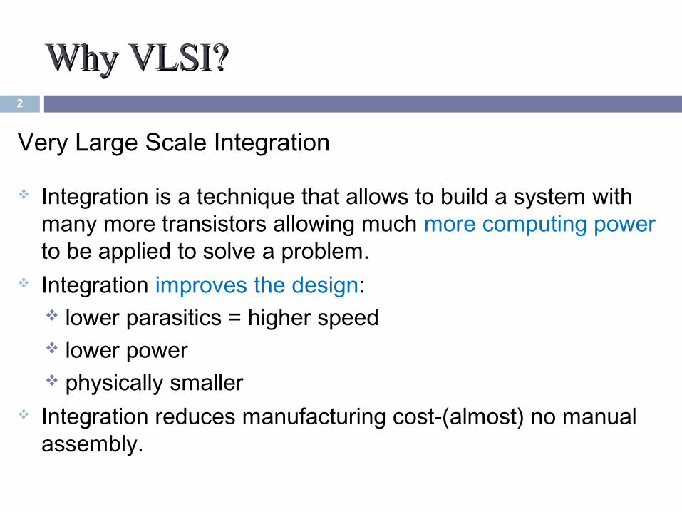
Why VLSI?Why VLSI?
Very Large Scale Integration
Integration is a technique that allows to build a system with many more transistors allowing much more computing power to be applied to solve a problem.
Integration improves the design: lower parasitics = higher speed lower power physically smaller
Integration reduces manufacturing cost-(almost) no manual assembly.
2
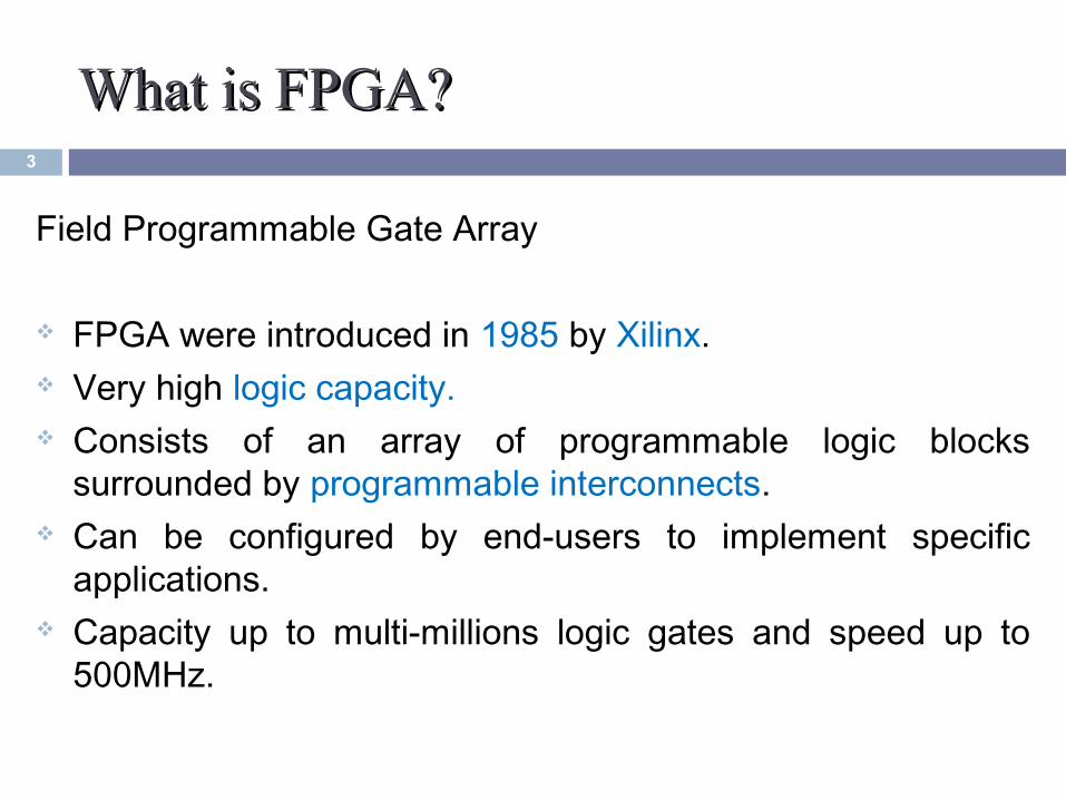
What is FPGA?What is FPGA?
Field Programmable Gate Array
FPGA were introduced in 1985 by Xilinx. Very high logic capacity. Consists of an array of programmable logic blocks
surrounded by programmable interconnects. Can be configured by end-users to implement specific
applications. Capacity up to multi-millions logic gates and speed up to
500MHz.
3
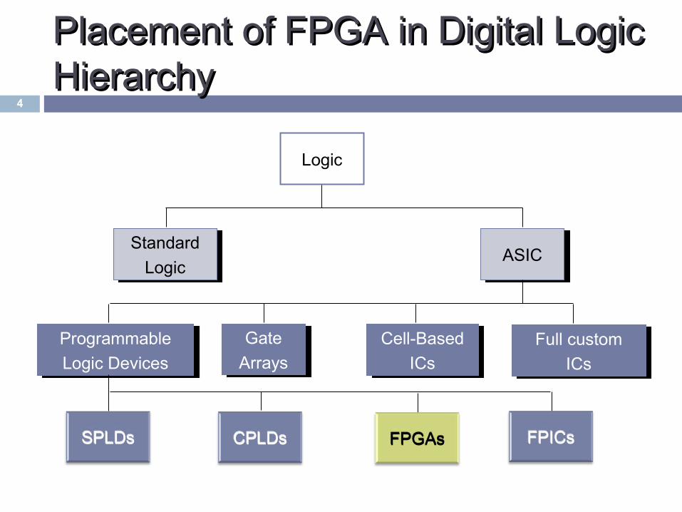
Placement of FPGA in Digital Logic Placement of FPGA in Digital Logic Hierarchy Hierarchy
4
Standard
Logic
Standard
Logic
Logic
ASICASIC
Full custom
ICs
Full custom
ICsCell-Based
ICs
Cell-Based
ICsGate
Arrays
Gate
ArraysProgrammable
Logic Devices
Programmable
Logic Devices
FPGAsCPLDsSPLDs FPICs
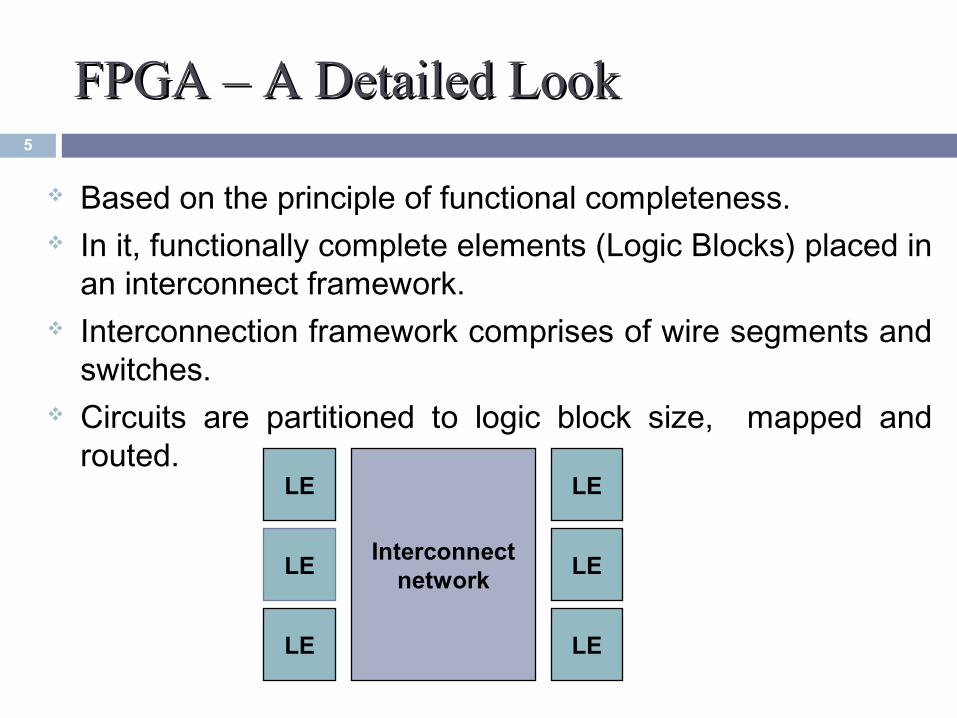
FPGA – A Detailed LookFPGA – A Detailed Look
Based on the principle of functional completeness. In it, functionally complete elements (Logic Blocks) placed in
an interconnect framework. Interconnection framework comprises of wire segments and
switches. Circuits are partitioned to logic block size, mapped and
routed.LE
LE
LE
Interconnectnetwork
LE
LE
LE
5
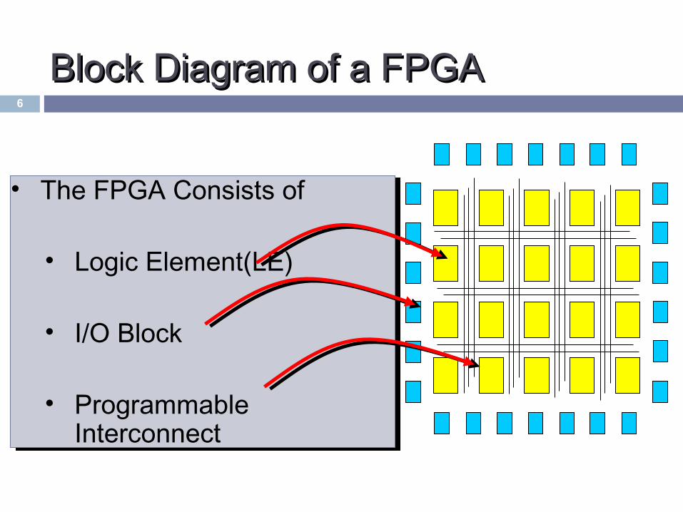
Block Diagram of a FPGABlock Diagram of a FPGA
• The FPGA Consists of
• Logic Element(LE)
• I/O Block
• Programmable Interconnect
• The FPGA Consists of
• Logic Element(LE)
• I/O Block
• Programmable Interconnect
6
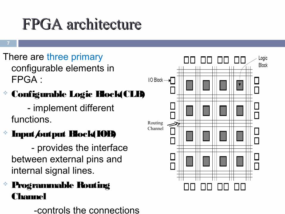
FPGA architecture FPGA architecture
There are three primary configurable elements in FPGA :
Configurable Logic Block(CLB)
- implement different functions.
Input/output Block(IOB)
- provides the interface between external pins and internal signal lines.
Programmable Routing Channel
-controls the connections among different blocks.
7
Routing Channel
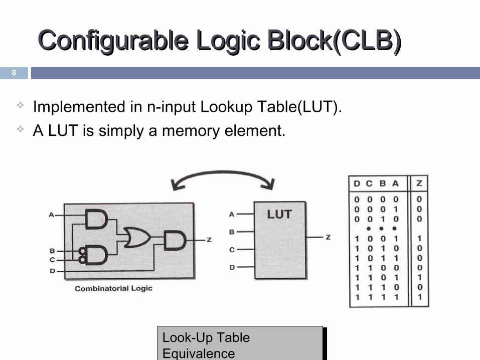
Configurable Logic Block(CLB)Configurable Logic Block(CLB)
Implemented in n-input Lookup Table(LUT). A LUT is simply a memory element.
8
Look-Up Table Equivalence
Look-Up Table Equivalence
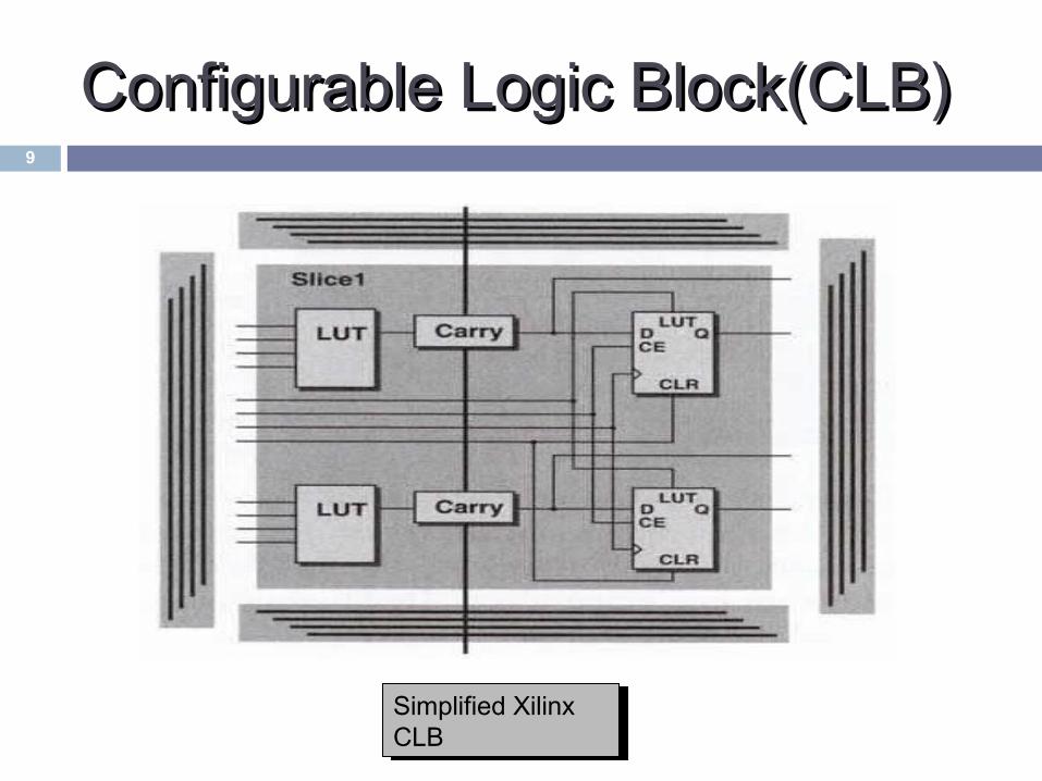
Configurable Logic Block(CLB)Configurable Logic Block(CLB)9
Simplified Xilinx CLB
Simplified Xilinx CLB
Configurable Logic Block(CLB)Configurable Logic Block(CLB)10
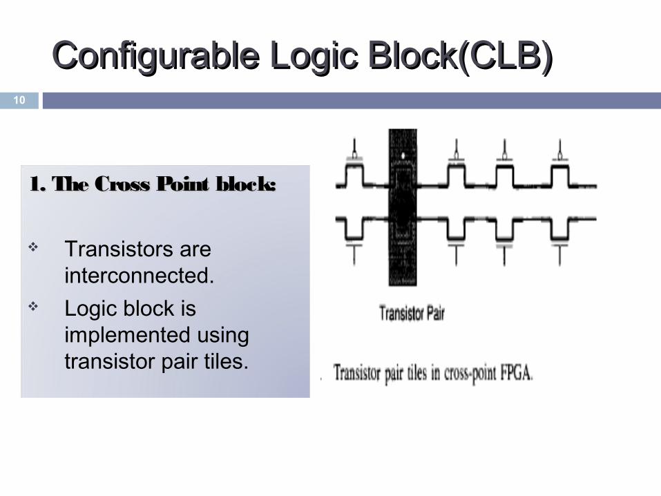
1. The Cross Point block:1. The Cross Point block:
Transistors are interconnected.
Logic block is implemented using transistor pair tiles.
Configurable Logic Block(CLB)Configurable Logic Block(CLB)11
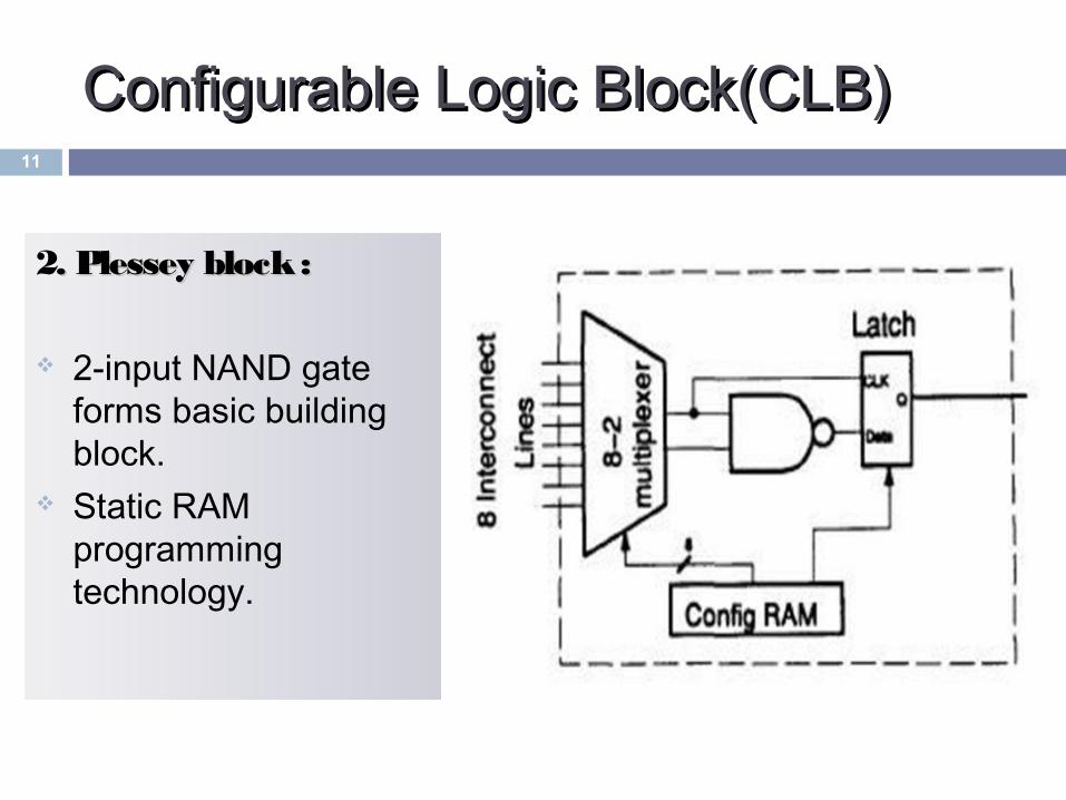
2. Plessey block :. Plessey block :
2-input NAND gate forms basic building block.
Static RAM programming technology.
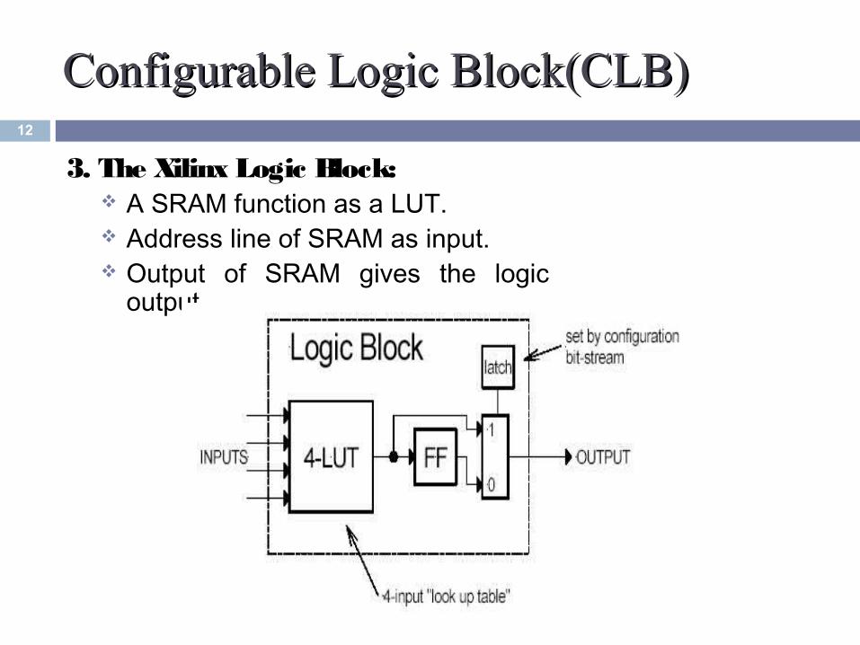
3. The Xilinx Logic Block: A SRAM function as a LUT. Address line of SRAM as input. Output of SRAM gives the logic
output.
Configurable Logic Block(CLB)Configurable Logic Block(CLB)12
Configurable Logic Block(CLB)Configurable Logic Block(CLB)13
4. Actel logic block :4. Actel logic block :
An Actel logic block consists of multiple number of multiplexers and logic gates.
If inputs of a multiplexer are connected to a constant or to a signal, it can be used to implement different logic functions.
Input/OutputInput/Output Block(IOBBlock(IOB))
Two types of IOBs are there 1)Dedicated for configuration of FPGA 2)User Configurable
Input/Output BlockInput/Output Block An IOB includes input and output registers, control signals,
muxes and clock signals. Unused FPGA inputs should not be left floating. Single-ended and differential operational modes are typically
supported
14
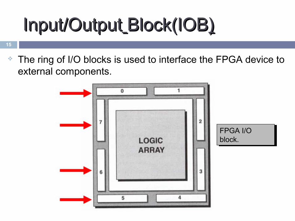
Input/OutputInput/Output Block(IOBBlock(IOB))
The ring of I/O blocks is used to interface the FPGA device to external components.
15
FPGA I/O block.
FPGA I/O block.
Programmable Routing ChannelProgrammable Routing Channel
Routing Channel-metallic conductor used to make connection. Three types are there
CLB Routing Channel : runs along each row and columns of CLBs.
IOB Routing Channel : forms CLB array & connects IOB with CLB routing channels.
Global Routing Channel : routes global signals (eg. Clock) with minimum delay.
Programmability in routing channels is obtained by using :(a)connection box and,
(b)switch box
16
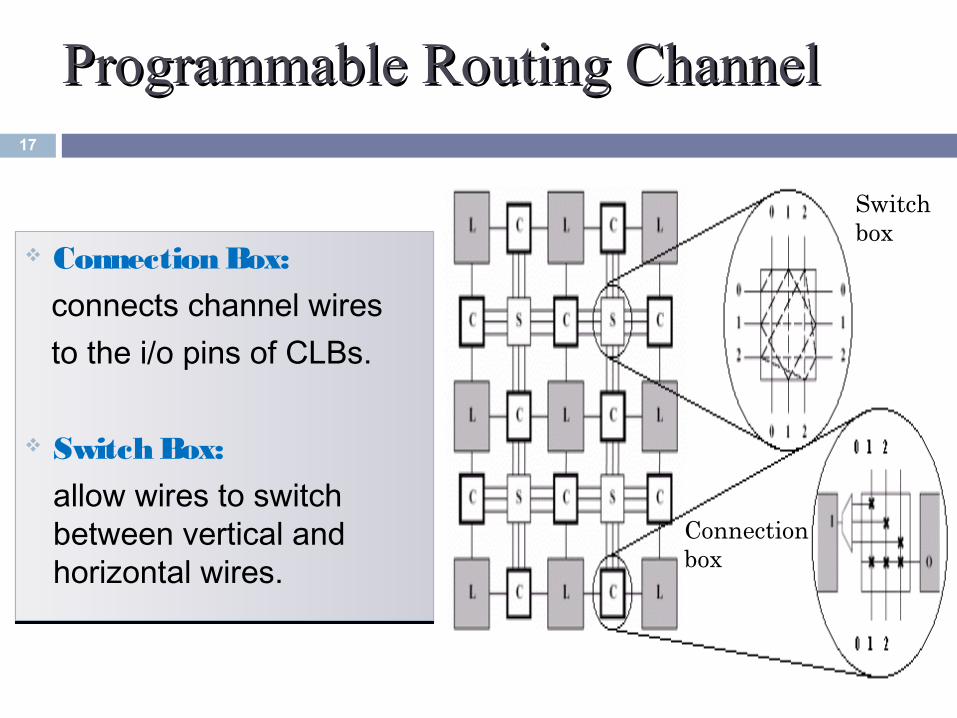
Programmable Routing ChannelProgrammable Routing Channel
Connection Box:
connects channel wires to the i/o pins of CLBs.
Switch Box:
allow wires to switch between vertical and horizontal wires.
Connection Box:
connects channel wires to the i/o pins of CLBs.
Switch Box:
allow wires to switch between vertical and horizontal wires.
Switch box
Connection box
17
Programmable Routing ChannelProgrammable Routing Channel
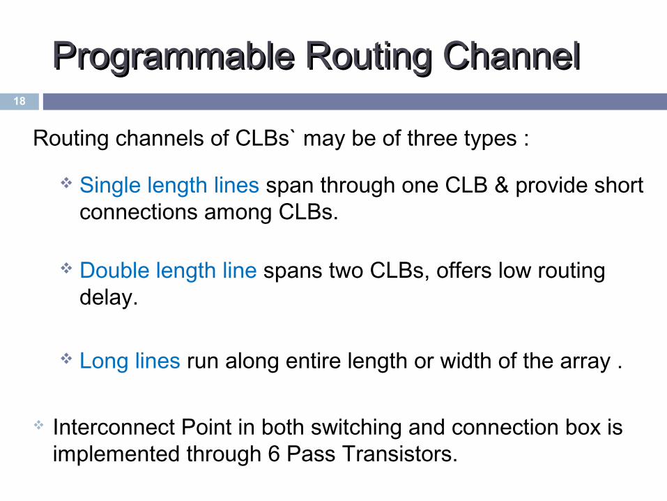
Routing channels of CLBs` may be of three types :
Single length lines span through one CLB & provide short connections among CLBs.
Double length line spans two CLBs, offers low routing delay.
Long lines run along entire length or width of the array .
Interconnect Point in both switching and connection box is implemented through 6 Pass Transistors.
18
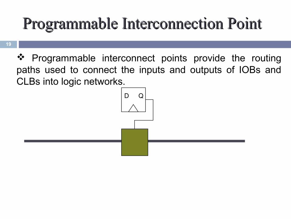
Programmable Interconnection PointProgrammable Interconnection Point
D Q
Programmable interconnect points provide the routing paths used to connect the inputs and outputs of IOBs and CLBs into logic networks.
19
Programmable wiring pathsProgrammable wiring paths
Organized into channels. Many wires per channel.
Connection between wire made at programmable interconnection points.
Must choose: Channels from source to destination. Wires within the channels
20
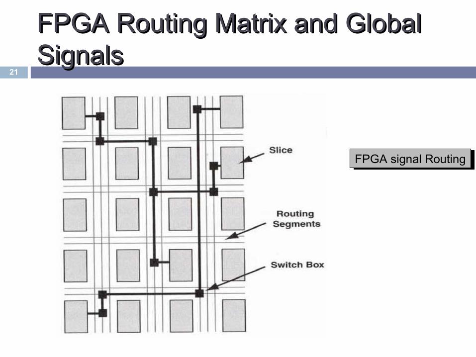
FPGA Routing Matrix and Global FPGA Routing Matrix and Global SignalsSignals
21
FPGA signal RoutingFPGA signal Routing
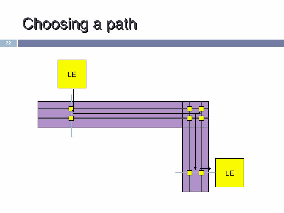
Choosing a pathChoosing a path22
LE
LE
FPGA MemoryFPGA Memory
Two primary types of memory within FPGAs. Distributed memory:
Takes advantage of the fact that LUT elements are implementation of SRAM memory blocks.
Block memory:The implementation of dedicated SRAM memory blocks
within the FPGA
23
FPGA DesignFPGA Design
FPGA manufacturer creates an FPGA fabric; system designer uses this fabric.
FPGA fabric design issues: Study sample user designs. Select interconnect topology. Create logic element
structures. Design circuits, layout.
Major levels of abstraction: Specification Architecture Logic Design Circuit Design Layout
24
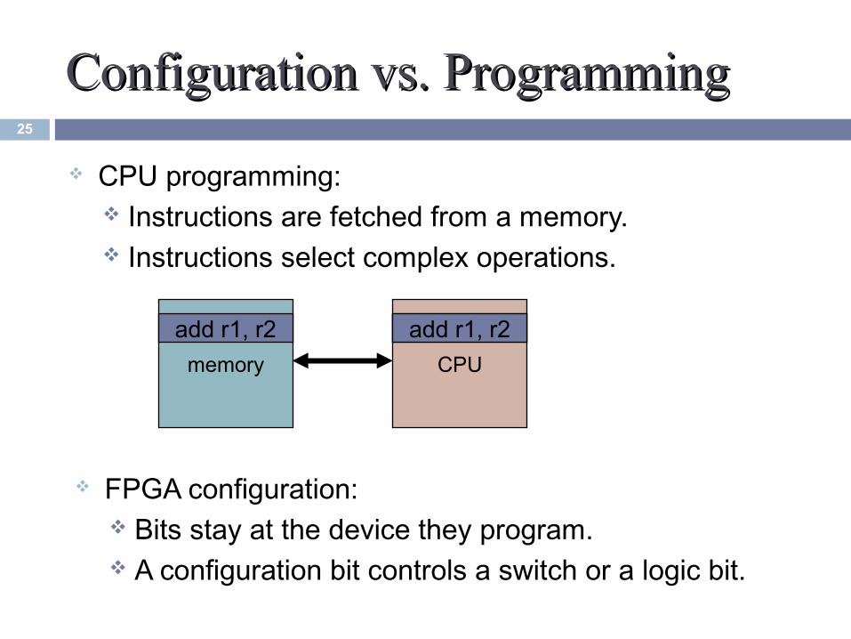
Configuration vs. ProgrammingConfiguration vs. Programming
FPGA configuration: Bits stay at the device they program. A configuration bit controls a switch or a logic bit.
CPU programming: Instructions are fetched from a memory. Instructions select complex operations.
CPUmemory
add r1, r2 IRadd r1, r2
25
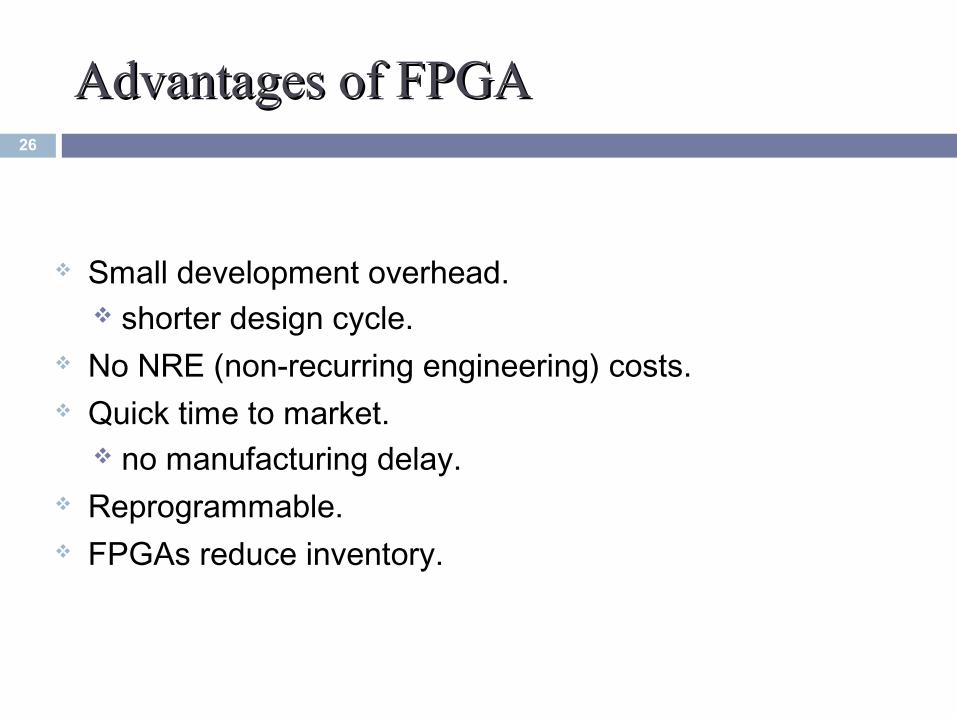
Advantages of FPGAAdvantages of FPGA
Small development overhead. shorter design cycle.
No NRE (non-recurring engineering) costs. Quick time to market.
no manufacturing delay. Reprogrammable. FPGAs reduce inventory.
26
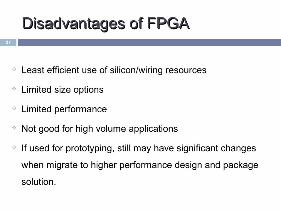
Disadvantages of FPGADisadvantages of FPGA
Least efficient use of silicon/wiring resources
Limited size options
Limited performance
Not good for high volume applications
If used for prototyping, still may have significant changes
when migrate to higher performance design and package
solution.
27
A NOVEL DESIGN OF A A NOVEL DESIGN OF A REVERSIBLE FIELD REVERSIBLE FIELD
PROGRAMMABLE GATE ARRAYPROGRAMMABLE GATE ARRAY
28
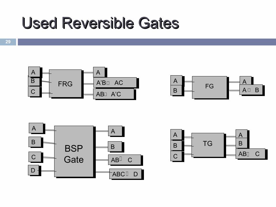
Used Reversible GatesUsed Reversible Gates29
FGFGAA
BBAAA BA B⊕
BB TGTGAA
CC
AABB
AB CAB C⊕
BB FRGFRGAA
CC
AA
A’B ACA’B AC⊕
AB A’C AB A’C ⊕
DD ABC DABC D
BBBSPGateBSPGate
AA
CC
AA
AB CAB C
BB
⊕
⊕
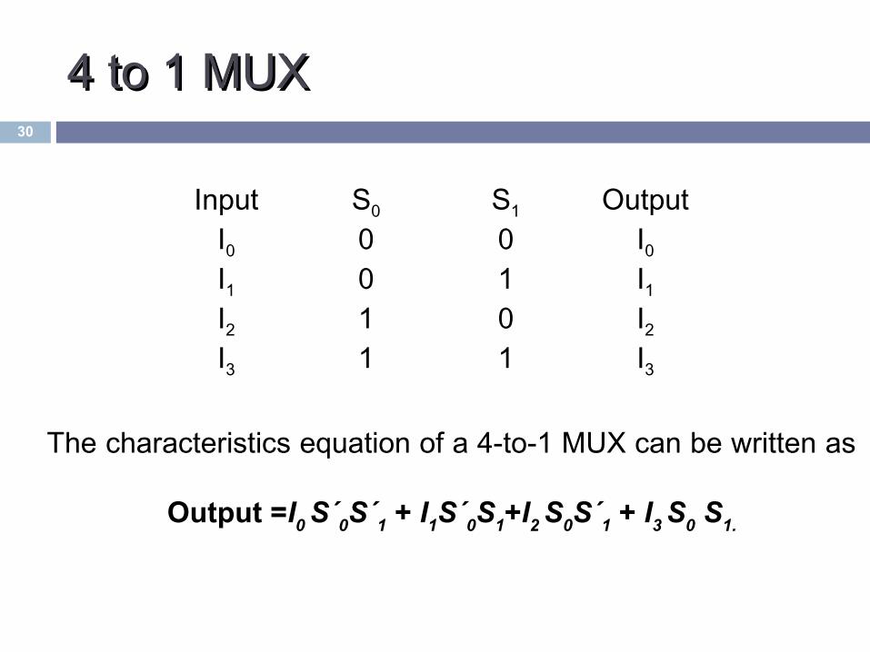
4 to 1 MUX4 to 1 MUX
Input S0 S1 OutputI0 0 0 I0
I1 0 1 I1
I2 1 0 I2
I3 1 1 I3
The characteristics equation of a 4-to-1 MUX can be written as
Output =I0 S´0S´1 + I1S´0S1+I2 S0S´1 + I3 S0 S1.
30
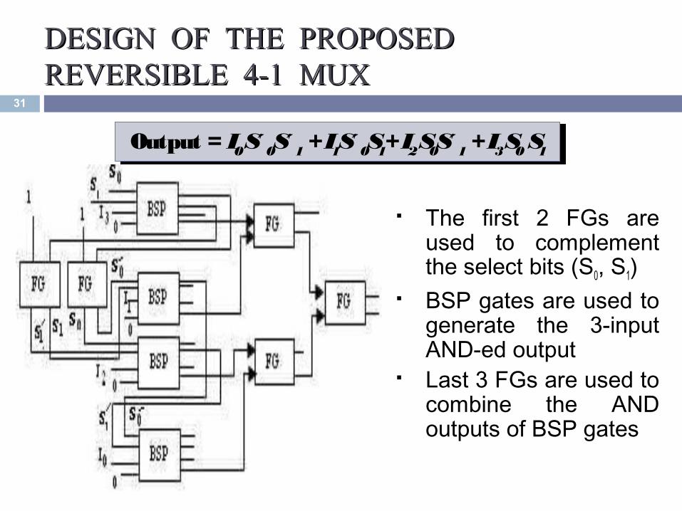
DESIGN OF THE PROPOSED DESIGN OF THE PROPOSED REVERSIBLE 4-1 MUXREVERSIBLE 4-1 MUX
Output = I0 S 0S 1 + I1S 0S1+ I2 S0S 1 + I3 S0 S1Output = I0 S 0S 1 + I1S 0S1+ I2 S0S 1 + I3 S0 S1
The first 2 FGs are used to complement the select bits (S0, S1)
BSP gates are used to generate the 3-input AND-ed output
Last 3 FGs are used to combine the AND outputs of BSP gates
31
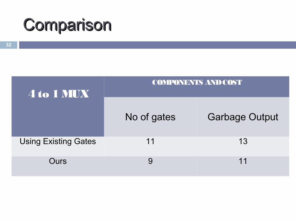
ComparisonComparison
4 to 1 MUXCOMPONENTS AND COST
No of gates Garbage Output
Using Existing Gates 11 13
Ours 9 11
32
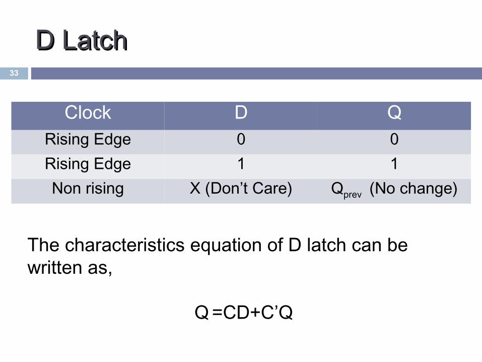
D LatchD Latch
Clock D QRising Edge 0 0Rising Edge 1 1Non rising X (Don’t Care) Qprev (No change)
33
The characteristics equation of D latch can be written as,
Q =CD+C’Q
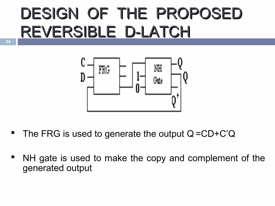
DESIGN OF THE PROPOSED DESIGN OF THE PROPOSED REVERSIBLE D-LATCHREVERSIBLE D-LATCH
34
The FRG is used to generate the output Q =CD+C’Q
NH gate is used to make the copy and complement of the generated output
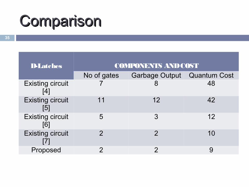
ComparisonComparison
D-Latches COMPONENTS AND COSTNo of gates Garbage Output Quantum Cost
Existing circuit [4]
7 8 48
Existing circuit [5]
11 12 42
Existing circuit [6]
5 3 12
Existing circuit [7]
2 2 10
Proposed 2 2 9
35
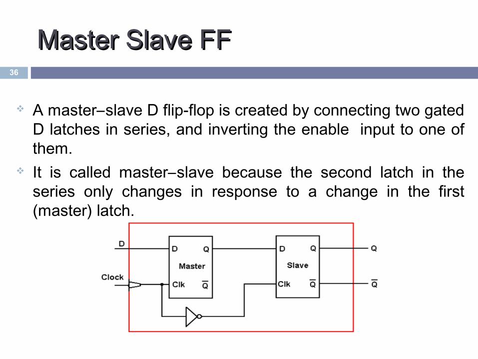
Master Slave FFMaster Slave FF
A master–slave D flip-flop is created by connecting two gated D latches in series, and inverting the enable input to one of them.
It is called master–slave because the second latch in the series only changes in response to a change in the first (master) latch.
36
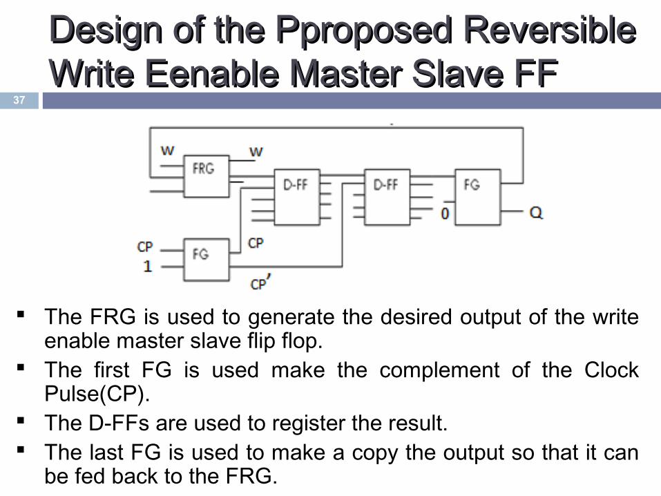
DesignDesign ofof thethe P Pproposedproposed R Reversibleeversible WWriterite E Eenableenable M Masteraster S Slavelave FF FF
The FRG is used to generate the desired output of the write enable master slave flip flop.
The first FG is used make the complement of the Clock Pulse(CP).
The D-FFs are used to register the result. The last FG is used to make a copy the output so that it can
be fed back to the FRG.
37
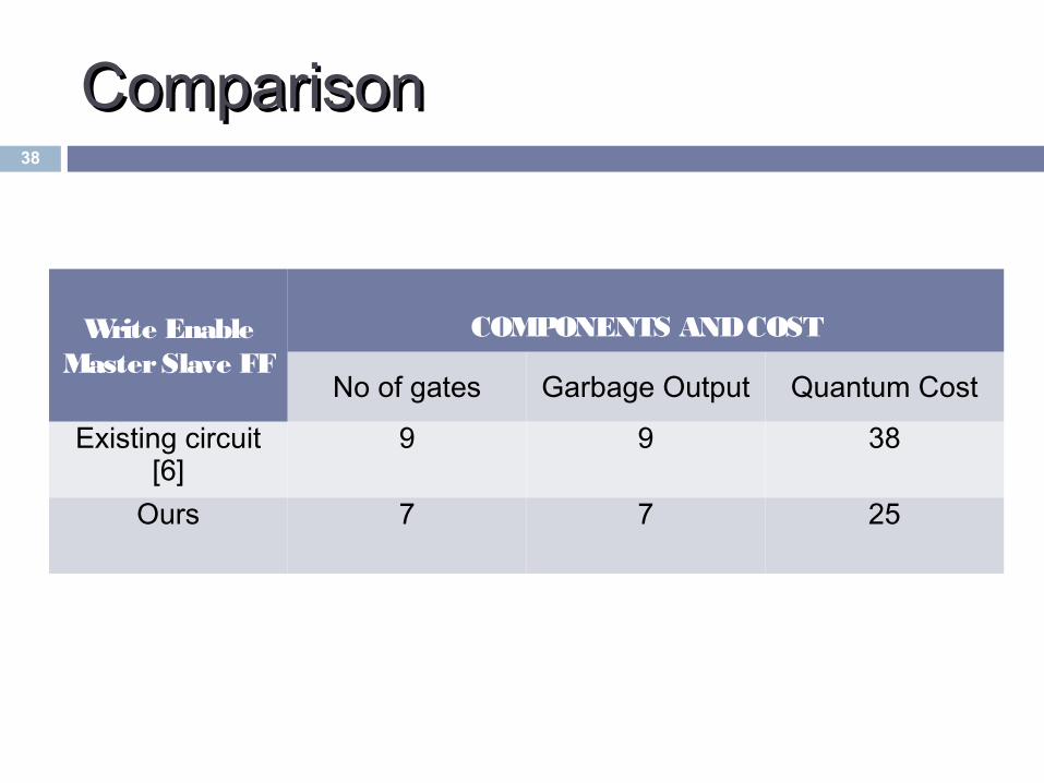
ComparisonComparison
Write Enable Master Slave FF
COMPONENTS AND COST
No of gates Garbage Output Quantum Cost
Existing circuit [6]
9 9 38
Ours 7 7 25
38
ConclusionConclusion
Here we presented the design of a first ever proposed reversible logic block of FPGA.
The sequential circuits that are used to realize the FPGA have been improved.
Efficiency of the proposed circuits is clearly highlighted by using comparison here.
The number of gates, number of garbage outputs and quantum cost have been reduced as well.
39
References
[1] R. Landauer, “Irreversibility and Heat Generation in the Computational Process” , IBM Jo urna l o f Re s e a rch a nd De ve lo pm e nt, vol. 3, pp. 183-191, 1961.
[2] C.H. Bennett, “Logical Reversibility of Computation”, IBM J. o f Re s e a rch a nd De ve lo pm e nt, pp. 525-532, November 1973.
[3] N. Huda, “On the Implementation of Reversible Random Access Memory”, M.Sc. thesis, Session: 2003-04, Department of CSE , University of Dhaka.
[4] H. Thapliyal, Vinod, A.P.,”Design of Reversible Sequential Elements with Feasibility of Transistor Implementation”, Circuits and Systems, 2007. ISCAS 2007. IEEE International Symposium on Volume, Issue , 27-30 May 2007 Page(s):625 – 628
[5] H. M. H. Babu, M. R. Islam, A. R. Chowdhury, and S. M. A. Chowdhury, “Reversible Logic Synthesis for Minimization of Full-Adder Circuit,” IEEE Conference on Digital System Design 2003; 50-4.
[6] H. M. H. Babu, M. R. Islam, A. R. Chowdhury, and S. M. A. Chowdhury, “Synthesis of Full-Adder Circuit Using Reversible Logic,” 17th International Conference on VLSI Design 2004; 757-60.
[7] Richard P. Feynman, “Quantum Mechanical Computers,” Foundations of Physics, vol. 16, no. 6, pp. 507-531, 1986.
40

Tha nk Tha nk Yo uYo u
41