FPGA implementation of synchronous and asynchronous counter and simulation of UART protocol
30
FPGA IMPLEMENTATION OF SYNCHRONOUS AND ASYNCHRONOUS COUNTER AND SIMULATION OF UART PROTOCOL BY: ASHIMA GUPTA ECE - 2 12310102811
-
Upload
ashima-gupta -
Category
Engineering
-
view
325 -
download
5
Transcript of FPGA implementation of synchronous and asynchronous counter and simulation of UART protocol

FPGA IMPLEMENTATION OF SYNCHRONOUS AND ASYNCHRONOUS COUNTER AND
SIMULATION OF UART PROTOCOL
BY: ASHIMA GUPTA
ECE-212310102811

FPGAA field programmable gate array (FPGA) is a semiconductor device containing programmable logic components and programmable interconnects. The programmable logic components can be programmed to duplicate the functionality of basic logic gates such as AND, OR, XOR, NOT or more complex combinational functions such as decoders or simple math functions.
CHARACTERSTICS:• 2-D array of logic blocks and flip-flops with programmable interconnections.• Compact design• User can configure :
*Intersections between the logic blocks *The function of each block
• FPGA programmed using electrically programmable switches• FPGAs are perfect for rapid prototyping of digital circuits
*Easy upgrades like in case of software*Unique application

HISTORY OF FPGA:BEFORE CPLD’S AND FPGA’S CAME INTO USE PLD’S I.E. PROGRAMMABLE LOGIC DEVICES WERE USED.PLD’S CAN BE PROGRAMMED TO PERFORM COMPLEX FUNCTIONS.IT CONTAINS AN ARRARY OF AND AND OR GATES.
THEY ARE BASICALLY OF THREE TYPES:
1. PROM( PROGRAMMABLE READ ONLY MEMORY) • IT OFFERS HIGH SPEED AND LOW COST.
2. PLA( PROGRAMMABLE LOGIC ARRAY)• FLEXIBLE FEATURES FOR MORE COMPLEX DESIGN.
3. PAL( PROGRAMMABLE ARRAY LOGIC)• GOOD FLEXIBILITY,FASTER AND LESS EXPENSIVE THAN PLA’S..
IN PLD’S PROGRAMS ARE MADE USING SOP EQUATIONS.SIMPLE PLD’SCOULD ONLY HANDLE 10 – 20 EQUATIONS AT A TIME.SO WE CAN’T FIT A VERY LARGE LOGIC DESIGN INTO JUST ONE OF THEM.ONE HAD TOBREAK THE LARGER DESIGNS AND FIT THEM INTO SET OF PLD’S.THIS WAS VERY TIME CONSUMING AND COMPLEX AS PLD’S HAD TO BEINTERCONNECTED WITH WIRES. THUS WE NEEDED CPLD’S AND FPGA’S.
STRUCTURE OF PAL

CPLD (COMPLEX PROGRAMMABLE LOGICAL DEVICE)
It contains a bunch of PLD blocks whose input and output are interconnected globally array.Thus it has two levels of programmability each PLD block can be programmed and then interconnections between PLD can be programmed.Some of the CPLD features are in common with PALs:• Non-volatile configuration memory. Unlike many FPGAs, an external configuration ROM isn't required, and
the CPLD can function immediately on system start-up.• For many legacy CPLD devices, routing constrains most logic blocks to have input and output signals
connected to external pins, reducing opportunities for internal state storage and deeply layered logic. This is usually not a factor for larger CPLDs and newer CPLD product families

CPLD ARCHITECTURE
A Complex Programmable Logic Device (CPLD) is a combination of a fully programmable AND/OR array and a bank of macrocells. The AND/OR array is reprogrammable and can perform a multitude of logic functions. Macrocells are functional blocks that perform combinatorial or sequential logic, and also have the added flexibility for true or complement, along with varied feedback paths.

FPGA CPLD
It contains 1,00,000 of tiny logic blocks. It contains only a few blocks of logic to a few thousands.
They are fine grained. They are coarse grained.
Usually for complex applications. Usually for simpler applications.
Made up of tiny logic blocks. Made up of larger blocks.
RAM based EEPROM based
Delays are more predictable. Delays are less predictable.
More expensive. Less expensive.
DIFFERENCES BETWEEN CPLD AND FPGA:
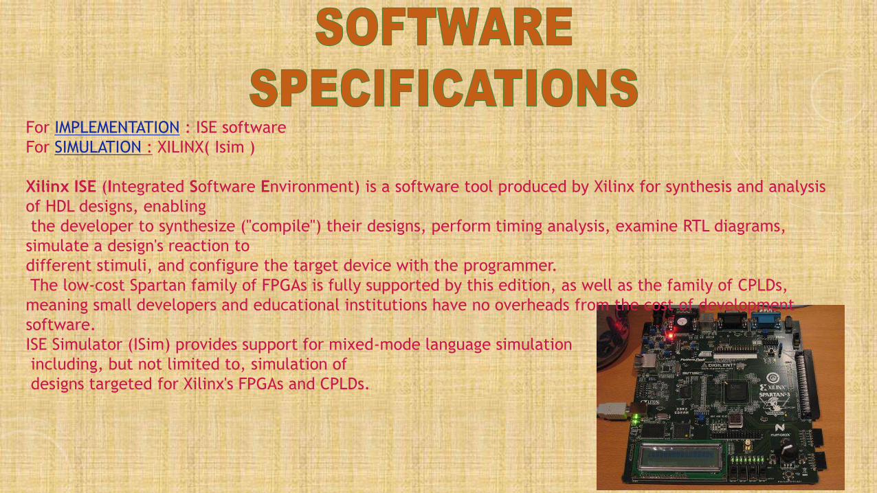
For IMPLEMENTATION : ISE software
For SIMULATION : XILINX( Isim )
Xilinx ISE (Integrated Software Environment) is a software tool produced by Xilinx for synthesis and analysis
of HDL designs, enabling
the developer to synthesize ("compile") their designs, perform timing analysis, examine RTL diagrams,
simulate a design's reaction to
different stimuli, and configure the target device with the programmer.
The low-cost Spartan family of FPGAs is fully supported by this edition, as well as the family of CPLDs,
meaning small developers and educational institutions have no overheads from the cost of development
software.
ISE Simulator (ISim) provides support for mixed-mode language simulation
including, but not limited to, simulation of
designs targeted for Xilinx's FPGAs and CPLDs.
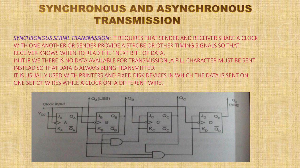
SYNCHRONOUS SERIAL TRANSMISSION: IT REQUIRES THAT SENDER AND RECEIVER SHARE A CLOCK WITH ONE ANOTHER OR SENDER PROVIDE A STROBE OR OTHER TIMING SIGNALS SO THAT RECEIVER KNOWS WHEN TO READ THE ‘ NEXT BIT ’ OF DATA.IN IT,IF WE THERE IS NO DATA AVAILABLE FOR TRANSMISSION ,A FILL CHARACTER MUST BE SENT INSTEAD SO THAT DATA IS ALWAYS BEING TRANSMITTED.IT IS USUALLY USED WITH PRINTERS AND FIXED DISK DEVICES IN WHICH THE DATA IS SENT ON ONE SET OF WIRES WHILE A CLOCK ON A DIFFERENT WIRE.

ASYNCHRONOUS SERIAL TRANSMISSION:
IT ALLOWS A DATA TO BE TRANSMITTED WITHOUT THE SENDER HAVING TO SEND A CLOCK SIGNAL TO RECEIVER.INSTEAD, SENDER AND RECEIVER MUST AGREE ON TIMING PARAMETERS IN ADVANCE AND SPECIAL BITS ARE ADDED TO EACH WORD WHICH ARE USED TO SYNCHRONIZE
SENDING AND RECEIVING UNITS.

SYNCHRONOUS COUNTER SIMULATIONCODE :
LIBRARY IEEE;
USE IEEE.STD_LOGIC_1164.ALL;
ENTITY SYNCCOUNTER IS
PORT ( VCC : IN STD_LOGIC;
CLK : IN STD_LOGIC;
RST : IN STD_LOGIC;
Q : INOUT STD_LOGIC_VECTOR(3 DOWNTO 0));
END SYNCCOUNTER;
ARCHITECTURE BEHAVIORAL OF SYNCCOUNTER IS
SIGNAL X,Y:STD_LOGIC;
COMPONENT FF IS
PORT(J,K,CLK,RST:IN STD_LOGIC;
Q:OUT STD_LOGIC);
END COMPONENT;
COMPONENT AND2 IS
PORT( A,B:IN STD_LOGIC;C:OUT STD_LOGIC);
END COMPONENT;

COMPONENT ANDGATE IS
PORT( A,B,C:IN STD_LOGIC;D:OUT STD_LOGIC);
END COMPONENT;
BEGIN
A:FF PORT MAP(VCC,VCC,CLK,RST,Q(0));
B:FF PORT MAP(Q(0),Q(0),CLK,RST,Q(1));
C:AND2 PORT MAP(Q(1),Q(0),X);
D:FF PORT MAP(X,X,CLK,RST,Q(2));
E:ANDGATE PORT MAP(Q(0),Q(1),Q(2),Y);
G:FF PORT MAP(Y,Y,CLK,RST,Q(3));
END BEHAVIORAL;
Output of synchronous counter

ASYNCHRONOUS COUNTER SIMULATIONCODE:
ENTITY COUNTER ISPORT ( VCC : IN STD_LOGIC;
CLK : IN STD_LOGIC;Q : INOUT STD_LOGIC_VECTOR(3 DOWNTO 0);RST : IN STD_LOGIC );
END COUNTER;
ARCHITECTURE BEHAVIORAL OF COUNTER ISCOMPONENT FF ISPORT(J,K,CLK,RST:IN STD_LOGIC;Q:OUT STD_LOGIC);END COMPONENT;
BEGINA:FF PORT MAP(VCC,VCC,CLK,RST,Q(0));
B:FF PORT MAP(VCC,VCC,Q(0),RST,Q(1));C:FF PORT MAP(VCC,VCC,Q(1),RST,Q(2));D:FF PORT MAP(VCC,VCC,Q(2),RST,Q(3));END BEHAVIORAL;
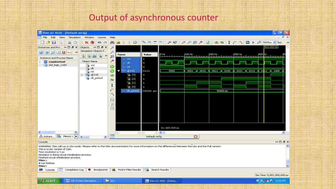
Output of asynchronous counter

UNIVERSAL ASYNCHRONOUS RECIEVER – TRANSMITTER(UART)
The Universal Asynchronous Receiver/Transmitter (UART) controller is the key component of the serial
communications subsystem of a computer. The UART takes bytes of data and transmits the individual bits in a
sequential fashion. At the destination, a second UART re-assembles the bits into complete bytes.
Serial transmission is commonly used with modems and for non-networked communication between computers,
terminals and other devices.
Asynchronous Serial Transmission
Asynchronous transmission allows data to be transmitted without the sender having to send a clock signal to the
receiver. Instead, the sender and receiver must agree on timing parameters in advance and special bits are added
to each word which are used to synchronize the sending and receiving units.

Block diagram of UART

TRANSMITTER HOLD REGISTER:
IF WE WANT TO WRITE A BYTE TO TRANSMITTER HOLD
REGISTER, IT IS AUTOMATICALLY TRANSFERRED TO
TRANSMITTER SHIFT REGISTER AND OUTPUT AS A SERIAL DATA
STREAM. IT'S OFFSET IS 0(DLAB=0).
RECEIVER BUFFER REGISTER:
IT IS USED TO STORE THE DATA BYTE RECEIVED. IT'S OFFSET IS
0(DLAB=0). THE DATA IN THIS REGISTER CAN BE ACCESSED BY
INPUT FUNCTIONS.
INTERRUPT ENABLE REGISTER:
THE INTERRUPT ENABLE REGISTER CONTROLS THE INTERRUPT
REQUEST. IT IS ALWAYS EQUAL TO ZERO. IT CAN NOT BE
ALTERED. THE FIRST BIT OF INTERRUPT ENABLE REGISTER IS FOR
INTERRUPTING WHEN A DATA BYTE IS RECEIVED. IF A DATA BYTE
IS RECEIVED AT THE RECEIVER BUFFER REGISTER AN INTERRUPT
IS RAISED.
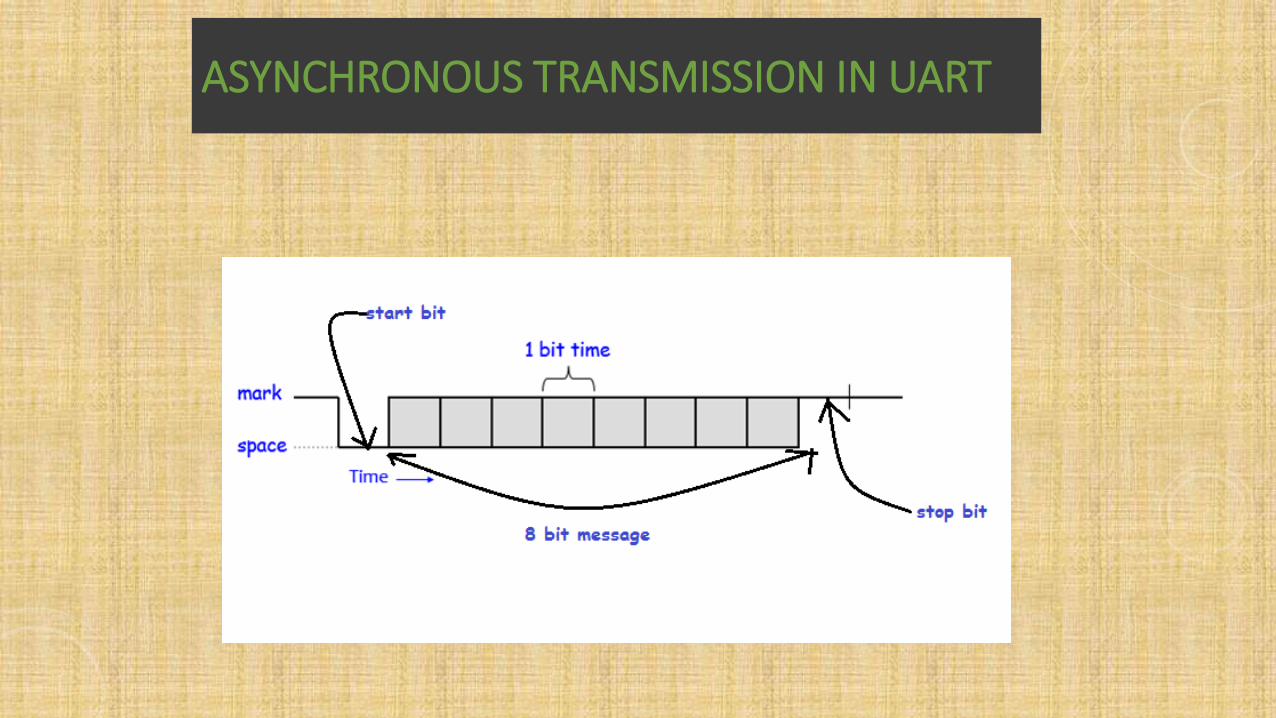
ASYNCHRONOUS TRANSMISSION IN UART
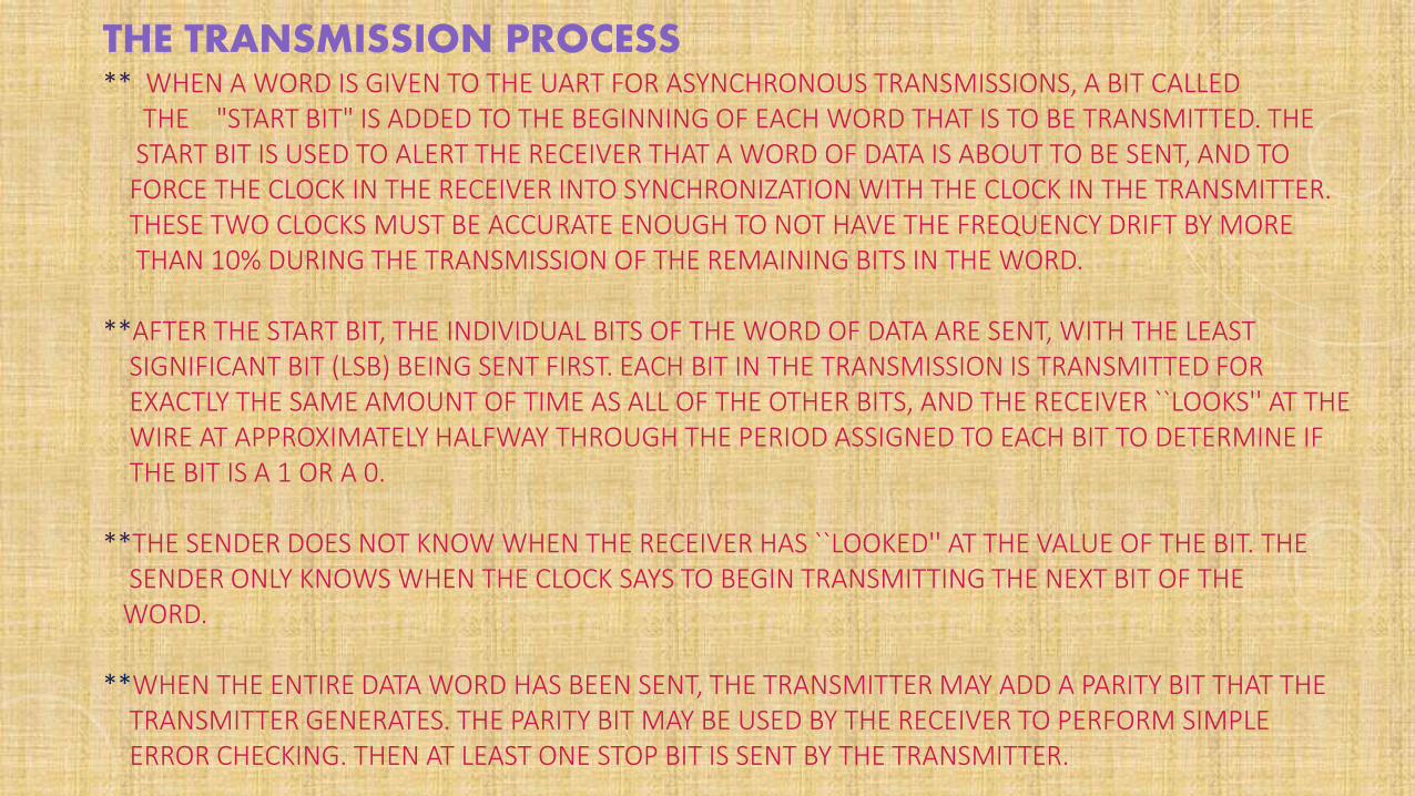
THE TRANSMISSION PROCESS** WHEN A WORD IS GIVEN TO THE UART FOR ASYNCHRONOUS TRANSMISSIONS, A BIT CALLED
THE "START BIT" IS ADDED TO THE BEGINNING OF EACH WORD THAT IS TO BE TRANSMITTED. THE START BIT IS USED TO ALERT THE RECEIVER THAT A WORD OF DATA IS ABOUT TO BE SENT, AND TO FORCE THE CLOCK IN THE RECEIVER INTO SYNCHRONIZATION WITH THE CLOCK IN THE TRANSMITTER.THESE TWO CLOCKS MUST BE ACCURATE ENOUGH TO NOT HAVE THE FREQUENCY DRIFT BY MORE THAN 10% DURING THE TRANSMISSION OF THE REMAINING BITS IN THE WORD.
**AFTER THE START BIT, THE INDIVIDUAL BITS OF THE WORD OF DATA ARE SENT, WITH THE LEASTSIGNIFICANT BIT (LSB) BEING SENT FIRST. EACH BIT IN THE TRANSMISSION IS TRANSMITTED FOREXACTLY THE SAME AMOUNT OF TIME AS ALL OF THE OTHER BITS, AND THE RECEIVER ``LOOKS'' AT THEWIRE AT APPROXIMATELY HALFWAY THROUGH THE PERIOD ASSIGNED TO EACH BIT TO DETERMINE IF THE BIT IS A 1 OR A 0.
**THE SENDER DOES NOT KNOW WHEN THE RECEIVER HAS ``LOOKED'' AT THE VALUE OF THE BIT. THESENDER ONLY KNOWS WHEN THE CLOCK SAYS TO BEGIN TRANSMITTING THE NEXT BIT OF THE
WORD.
**WHEN THE ENTIRE DATA WORD HAS BEEN SENT, THE TRANSMITTER MAY ADD A PARITY BIT THAT THETRANSMITTER GENERATES. THE PARITY BIT MAY BE USED BY THE RECEIVER TO PERFORM SIMPLEERROR CHECKING. THEN AT LEAST ONE STOP BIT IS SENT BY THE TRANSMITTER.

BAUD RATE
• Baud is a measurement of transmission speed in asynchronous communication.
Traditionally, a Baud Rate represents the number of bits that are actually being sent over the media, not the
amount of data that is actually moved from one DTE device to the other. The Baud count includes the
overhead bits Start, Stop and Parity that are generated by the sending UART and removed by the receiving
UART. This means that seven-bit words of data actually take 10 bits to be completely transmitted.
Therefore, a modem capable of moving 300 bits per second from one place to another can normally only
move 30 7-bit words if Parity is used and one Start and Stop bit are present.
• Baud rate is calculated as
Baud rate = Main reference frequency/(16*divisor)
• In order to use the UART you need to know what baud rate you want to transmit at. The transmitter and receiver modules have been designed with a clock divider inside, which runs 16 times slower than the clock signal sent to it. Therefore, there should be a clock divider running at 16 times the baud rate driving the UART modules.

BAUD RATE EXAMPLE:
IF FOR EXAMPLE, YOU WANT TO TRANSMIT AT 33.6 KBPS AND THE FPGA BOARD RUNS AT 25.175 MHZ THEN:
BAUD RATE X 16 = 33600 X 16 = 537600
CLOCK DIVISION RATIO = 25175000 / 537600 = 46
CLOCK DIVISOR = 46 / 2 = 23
THEREFORE, THE CLOCK DIVIDER USED TO CLOCK THE UART WOULD HAVE A DIVISOR OF 23. THIS WOULD GIVE A TRANSMISSION RATE OF ABOUT 34.2 KBPS.
THE IMPLEMENTED UART MODULE HAS 12 I/O PORTS, WHICH ARE USED TO CONTROL IT, GET I/O TO AND FROM IT, AND TO DETERMINE IT’S STATUS.

SERIAL COMMUNICATION BLOCK DIAGRAM
Processor/ Controller
UARTPeripheral
RS-232Transceiver
MAX 232

MICROPROCESSOR:
• 8085 IC -40 pin• It’s a single chip semiconductor or a simple computer on a chip• Used to perform arithmetic and logical operations.• Used to interface different IC’s to perform different work.• It’s a stand alone device.• We have to externally connect RAM,ROM,I/O etc..• Used in higher and industrial projects.
MICROCONTROLLER:
• Its consists of CPU,RAM,ROM and other peripherals.• Used to perform specific tasks in which relation between input and output is defined.• Used in lower end projects.
RS-232:
RS-232 is the traditional name for a series of standards for serial binary single ended data and control signals between DTE(data terminal equipment) and DCE(data circuit terminating equipment).Its used in serial ports which are used for connection to modems , printers , mouse etc..The minimal 3 wire RS-232 connection consists of transmit data,receive and ground.

PIN CONFIGURATION of RS-232:
PIN NO. NAME TYPE
1 DATA CARRIER DETECT I/P
2 RECEIVED DATA I/P
3 TRANSMITTED DATA O/P
4 DATA TERMINAL READY O/P
5 SIGNAL GROUND COMMON
6 DATA SET READY I/P
7 REQUEST TO SEND O/P
8 CLEAR TO SEND I/P
9 RING INDICATOR I/P

ASYNCHRONOUS CONNECTION
STATE DIAGRAM :
At transmitter end…
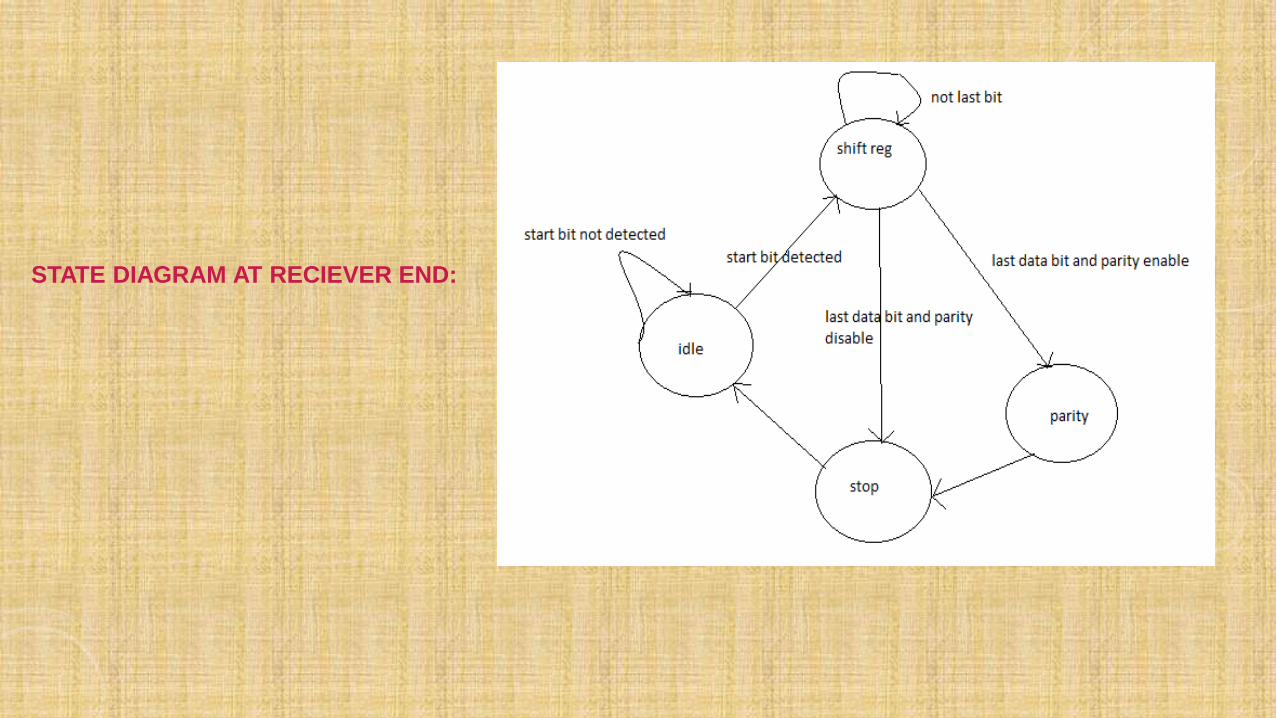
STATE DIAGRAM AT RECIEVER END:

APPLICATIONS OF UART:
**Communication between distant
computers:
• Serializes data to be sent to modem
•De-serializes data received from modem
**PC serial port is a UART!
Serializes data to be sent over serial cable
De-serializes received data

UART SIMULATION AT TRANSMITTER END:
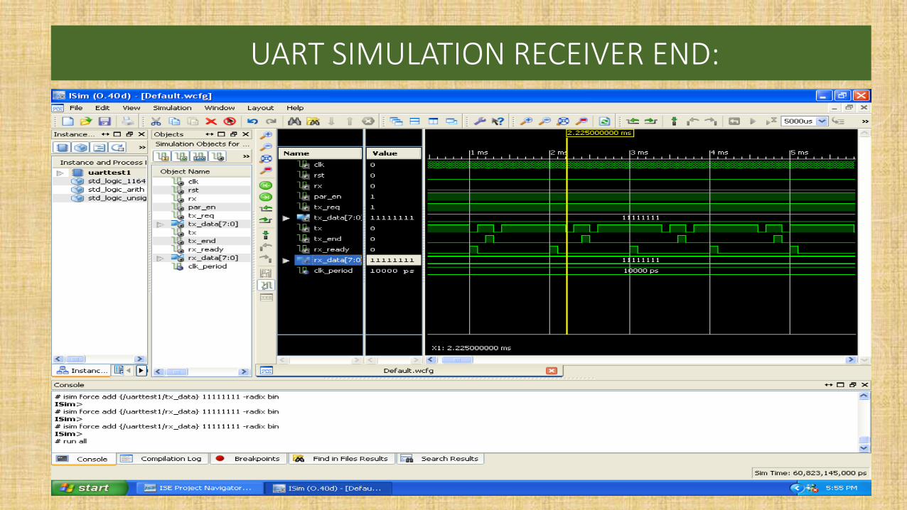
UART SIMULATION RECEIVER END:
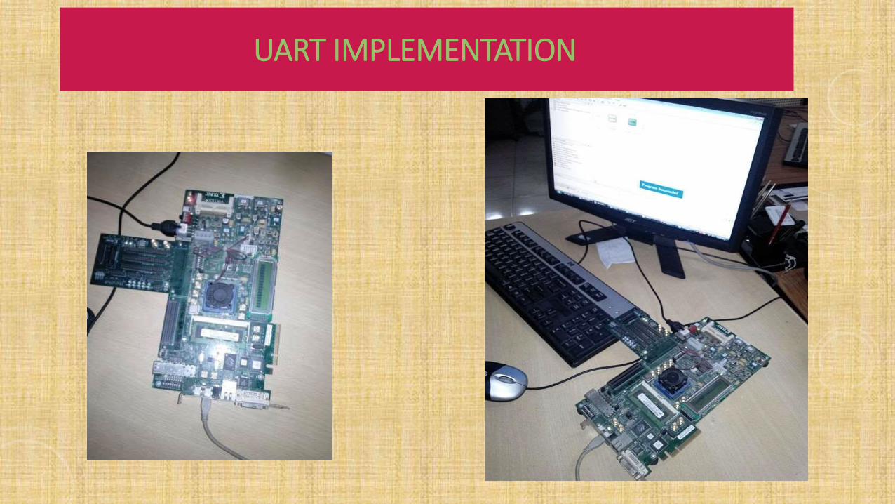
UART IMPLEMENTATION

THANK YOU….
By: ASHIMA GUPTAECE 2 GRP 112310102811


![[PPT]UART and UART Driver - University at Buffalobina/cse321/fall2009/UARTDriver.ppt · Web viewUART and UART Driver B. Ramamurthy * UART UART: Universal Asynchronous Receiver/Transmitter](https://static.fdocuments.us/doc/165x107/5b2ab3637f8b9a55068b752f/pptuart-and-uart-driver-university-at-binacse321fall2009uartdriverppt.jpg)