Modular Exponentiation - Centro de Investigaci³n y de Estudios

FPGA Implementation of Modular
Exponentiation Using Single Modular Multiplier
M. Issad, B. Boudraa, M. Anane, S. Seddiki
Abstract— This paper presents the FPGA implementation of
Modular Exponentiation (ME), based on Software/Hardware
(SW/HW) approach. Indeed, in Rivest, Shamir and Adleman (RSA)
cryptosystem, ME which is computed by series of Modular
Multiplications (MM’s), is the main function to encrypt and decrypt
data. In order to achieve the best trade-off between area, speed and
flexibility, we propose in this work an embedded system, where
ME algorithm is managed in SW, using the processor MicroBlaze
of Xilinx. The MM is implemented as a HW core around the
processor. Because, the MM is usually considered as a critical
arithmetic operation, the Montgomery modular multiplication,
requiring simple shifts and additions is used to realize the HW
architecture of our MM core. The results show that the application
to RSA 1024-bits, the execution time of the ME is about 109.5 ms.
While, in terms of hardware resources, the device requires 1645
slices.
Keywords— Modular Exponentiation, Montgomery Modular
Multiplication, Microblaze, RSA.
I. INTRODUCTION
Modular Exponentiation (ME) is a common function
used in several public key cryptosystem, such as, Rivest,
Shamir and Adleman (RSA) protocol [1] and Diffie-Hellman
key exchange scheme [2].
Most algorithms developed in literature for computing
the ME, have shown that this function is based on the
iterative computation of the modular multiplication. In order
to optimize the performance execution of the basic
arithmetic operation, namely, the modular multiplication, an
efficient algorithm was developed by Montgomery [3]. This
algorithm transforms the modulus reduction to a series of
additions and right shifts. Therefore, the implementation of
RSA requires two parts. The first part is dedicated to the
calculation of the Montgomery modular multiplications
(MMM’s). The second one is used to control the execution
of the ME.
In this paper, our main aim is the Software/Hardware
(SW/HW) implementation of the ME for RSA. The
proposed embedded system is based on the soft processor
core MicroBlaze [4].
This work was supported by the Ministère de l’Enseignement
Supérieures et de la Recherche Scientifique, Algeria.
M. Issad is with the Centre de Développement des Technologies Avancées, Cité 20 Aout 1956, Baba Hassen BP 17, Algeries, Algeria
(email: [email protected]).
B.Boudraa is with the Université des Sciences et de la Technologie Houari Boumediene, Bab ezzouar, Algeria (email: [email protected]).
M.Anane is with the Ecole Supérieur d’informatique, Oued Smar,
Algeria (email: [email protected]). S. Seddik is with the Centre de Développement des Technologies
Avancées, Cité 20 Aout 1956, Baba Hassen BP 17, Algeries, Algeria
(email: [email protected]).
Indeed, although the timing complexity optimization is
still a major problem of cryptographic systems designers, the
enhancement in terms of hardware resources and flexibility
remains a binding constraint. Therefore, in order to achieve
the best trade-off between area, speed and flexibility, we
propose to implement in HW single Montgomery modular
multiplier. The overall control of the ME algorithm is
completely executed in SW by the processor Microblaze.
However, in such implementations, the MMM requires
first an optimisation, in order to adapt its execution to the
processor data path. In this work, we propose also a high
radix implementation of the MMM, based on its sequential
version [5].
The rest of this paper is organized as follows: In section
II, the RSA algorithm is described. In section III, the MMM
and the proposed method for its hardware implementation
are presented. In section IV, we present the modular
exponentiation algorithm. In Section V, the FPGA
methodology of the proposed embedded system is reported.
Section VI, discusses the experimental results and some
comparisons with some recent works. The conclusion is
given in section VII.
II. RSA ALGORITHM
Generally, the implementation of RSA requires the
design of three abstraction levels [1].
The first level corresponds to cryptographic schemes
where the public key (E, N) and the private key (D, N) are
first generated. To calculate N, E and D, two large random
prime numbers p and q are generated and two equations are
used:
qpN (1)
1)] - (q × 1) -[(p mod 1 E ×D (2)
E is chosen in the range 1 < E < (p - 1) × (q - 1) such that,
1 =1)] - (q × 1) -(pgcd[E, (3)
The key (E, N) is made public. p, q and D are kept secret.
Therefore, breaking the RSA security is believed to be as
hard, because crackers will never know the values of p and
q. Even though, E and N are known, it is still hard to find D.
The second level consists of the ME computation.
Indeed, to encrypt a plaintext message M and decrypt the
encrypted message P, we apply the expressions (4) and (5),
respectively.
Recent Advances in Electrical and Computer Engineering
ISBN: 978-1-61804-228-6 162
NmodMP E (4)
NmodPM D (5)
E and D are respectively the public and the private
exponents. N is the modulus.
The third level is often considered as the calculation of
the modular multiplication over Galois field GF(N) [6]. This
operation can be executed by using multiplication and
division. However, in literature many methods are proposed
to compute the modular multiplication in order to avoid the
division, as this latter is a complex operation. Among these
methods, MMM is often used.
III. MONTGOMERY MODULAR MULTIPLICATION
The MMM using radix r (r=2k) of two operands X and Y
is defined by the following expression [3]:
S=X×Y×R-1
mod N (6)
N is an odd integer coded on n digits. R is the Montgomery
constant, chosen such that R = 2k×n
, with pgcd (2k, N) = 1. In
the RSA, this condition is satisfied, because N is an odd
number.
Since the MMM result is obtained with additional factor,
namely R-1
, the MMM requires the conversion of X and Y to
Montgomery representation and then performs the
expression (6). The result is converted back to recover it in
the classical domain [3].
Many works have been conducted on the hardware
implementation of the MMM [7], [8] in order to improve its
execution time. However, the resulting architectures require
more resources and are not applicable for the design that we
target. In [9], we have proposed an approach using radix-2,
in order to reduce the occupied resources. The results
showed low temporal performances, because the MMM
radix-2 algorithm requires high number of iterations.
Indeed, the effective approach to implement the MMM
around the embedded processor is to use its sequential
version (Digit-serial) [5]. In this version, inputs and output
of the algorithm are first decomposed into n digits of k bits,
2k
being the chosen radix. Then arithmetic operations are
performed digit-by-digit in a serial mode. In addition, to
adapt the execution of the MMM to the processor, the
intuitive choice of the parameter k corresponds to the data
path size of the processor. In this work, as we use
Microblaze which is a 32 bits soft core, the value of k is of
32.
In the original MMM algorithm, a final subtraction is
used at the end. This subtraction is necessary because the
operands X and Y must satisfy the condition 0 ≤ X, Y<N.
However, the reduction of S mod N if S ≥ N can be omitted
using a modified version of the MMM algorithm. In this
case, inputs and output can be higher than N (0≤X, Y,
S<2×N) with R=2(n+1)×32
. Then, the operands X and Y
become coded on (n+1) instead of n digits. Our work is
based on this variant, called MMM algorithm without final
subtraction [10].
Indeed, the MMM algorithm is based on the iterative
calculation of the intermediate results S(i+1) which are given
by the expression (7) [5].
32
)i()i()1i( 2/))Nq()Y]i[X(S(S (7)
In radix r=232
, the operands X, Y, the modulus N and the
intermediate results S(i+1) are represented by:
n
0i
32i2]i[XX ,
n
0j
32j2]j[YY ,
n
0j
32j2]j[NN
n
0j
32j
)1i()1i( 2]j[SS ,
with N[n]=0.
As the operands are coded on succession of digits, to
calculate S(i+1), an outer and an inner loops are used. They
are defined respectively by the indices (i) and (j). denotes
the (i)th
digit of the operand X. (j) defines the digit-position
of Y, N and S(i). Thus, at each iteration (i) where only one
digit of the operand X is selected, we begin by the
computation of q(i) using the expressions:
q(i)=(H[0](i)×N') mod 232
(8)
where, H[0](i) =S[0](i)+(X[i]×Y[0]) and N'=-N[0]-1
mod 232
Then, the arithmetic operations are performed using digit-
serial mode with a precision of 32 bits. To obtain S(i+1), we
have used two intermediate variables H(i) and W(i). The
values of their (j)th
digits, i.e., H[j](i) and W[j](i) depend on
both multiplications X[i]×Y[j] and q(i)×N[j], respectively. If
we consider that,
X[i]× Y[j]= Pr1[j](i) + (C1[j](i) ×232
) (9)
and
q(i)× N[j]= Pr2[j](i) + (C2[j](i) ×232
), (10)
therefore H[j](i) and W[j](i) are written as:
)]j[H,2cy,2cy( )i(
32j
1
32j
2 Pr1[j](i)+ C1[j-1](i)+
S[j](i) +1
21
1
jj
cycy (11)
)]j[W,2cy,2cy( )i(
32j
3
32j
4 Pr2[j](i)+ C2[j-1](i)+
H[j](i) +1
41
3
jj
cycy (12)
with j varying from 0 to n.
C1[j-1](i) and C2[j-1](i) are the most significant digits of both
multiplications, respectively. cy1j-1
, cy2j-1
and cy3j-1
,
cy4j-1
are the carriers calculated at the iteration (j-1). These
carriers, as C1[j-1](i) and C2[j-1](i), are initialized at the
beginning of the (i)th
loop. Using these notations, the
computation of the expressions (11) and (12) may be carried
out sequentially, where we calculate first the (j)th
digit of H(i)
followed by the (j)th
digit of W(i). Then, according to the
expression (7), the (j)th
digits of the intermediate results
S(i+1) are obtained considering only the (n+1) most
significant digits of W(i).
In order to implement the MMM in embedded
cryptosystem, the arithmetic operations presented above are
performed in an Arithmetic Unit (AU). In the following, we
present its hardware implementation.
Hardware Implementation of the Arithmetic Operations
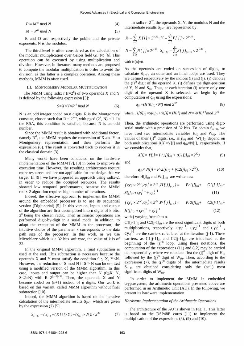
The architecture of the AU is shown in Fig. 1. This latter
is based on the DSP48E cores [11] to implement the
multiplication of the expressions (8), (9) and (10).
Recent Advances in Electrical and Computer Engineering
ISBN: 978-1-61804-228-6 163

MicroBlaze
PLB
UART Timer
BRAM
DLMB
ILMBMM Core
Y[j]X[i]
Pr1[j](i)
From memories
Reset_cy12clk
S[j](i)
clk
H[j](i)
q(i)
cy1
En_q(i)
C1[j](i)
Add1clk
cy2Add2
clk
clkN’ Pr2[j](i)
Reset_cy34clk
W[j](i)
cy3
C2[j](i)
Add3clk
cy4
Add4clk
N[j]
From memory
Arithmetic Unit
3232
32
32
32
32
32
32
32
32
32
32
32
Mul3
Mul2
Mul1
Reg
D
Reg
D
Reg
D
D
clk
clk
FIFO32 32
Fig.1 Architecture of the Arithmetic Unit
It consists of three multipliers, four carry propagate
adders, registers and D flip-flops. The implementation of the
expression (7) supposes that the operands X, Y and N are
stored in memories. The intermediate results S(i) are stored in
FIFO. Indeed, at each iteration (i), where the (i)th
digit of the
operand X is selected, the value of q(i) can be considered as
constant. q(i) is calculated by the Mul2 according to the
expression (8). In addition to the input data, the AU receives
three control signals which are En_q(i), Reset_cy12, and
Reset_cy34. The first allows to maintain q(i) constant. The
second and the third are used respectively to initialize the
carries (C1[j-1](i), cy1j-1
, cy2j-1
) and (C2[j-1](i), cy3
j-1 , cy4
j-1)
at the beginning of the iteration (i). Carries are delayed by
one clock cycle and added with the next computed digits.
Therefore, the computation of the (j)th
digit of W(i) is split
into six clock cycles as flow:
1. Address generation to get Y[j].
2. Reading Y[j] from memory and computing the product
X[i]×Y[j] by the Multiplier Mul1.
3. Computation of H[j](i) by the adders add1 and add2.
4. Address generation to get N[j].
5. Reading N[j] from memory and computing the product
q(i)×N[j] by the Multiplier Mul3.
6. Computation of W[j](i) using the adders add3 and add4.
Thus, to compute the expressions (11) and (12), where (j)
varying from 0 to n, the iteration (i) requires (n+1) cycles.
Taking into account the number of cycles corresponding to
W[j](i) computation and the size of the operand X, the clock
cycle count CCC to get the MMM result is given by the
expression (13).
2)+(n ×7)+(nCCC (13)
IV. MODULAR EXPONENTIATION ALGORITHM
For large exponents, the modular exponentiation is a
complex function. Since, many algorithms have been
developed to optimize its performances. In our work, the
binary R-L (Right to Left) method is utilized [12]. This latter
is based on the binary representation of the exponent
scanned bit-by-bit from Right to Left. At each iteration of
the algorithm, squaring and multiplication are performed.
The multiplication is executed only if each bit of the
exponent is equal to 1. The binary R-L algorithm is given
below.
Binary R-L Algorithm
Inputs: ∑
∑ , ∑
,
Pre- computed: N’=-N[0]-1 mod 232 , with pgcd (N, 232)=1
R2 mod N, with R=2 (n+1)×32
Intermediate variables: ∑ ,
∑
Output : M = ∑ =PD mod N
Begin
1. Sq-1= Montgomery(X, R2 mod N, N, N’)
2. CC-1= Montgomery(1, R2 mod N,N N’)
3.
4. Sqi= Montgomery(Sqi-1, Sqi-1, N, N’)
5. If = 1 then CCi=Montgomery(CCi-1, Sqi-1, , N, N’)
6. else CCi = CCi-1
7. end for
8. M=Montgomery(CCe-1, 1, N, N’)
Return M
In this algorithm, input/output data and intermediate
results are represented in radix r=232
, except the exponent D,
coded in radix 2. The Montgomery(.) function corresponds to
the computation of the MMM. At each iteration, it receives:
two operands, the modulus and the constant N’ to provide
two intermediate results denoted by CCi and Sqi. These
results correspond to the modular multiplication and
squaring, computed in the Montgomery domain,
respectively.
V. ARCHITECTURE OF THE EMBEDDED SYSTEM
The hardware architecture of the proposed embedded
system for computing the modular exponentiation is shown
in Fig. 2.
Fig.2 Hardware architecture of the embedded system
This architecture was built on Xilinx Virtex-5 XC5VLX50T Genesys development board [13] and
designed using XPS 13.2 (Xilinx Platform Studio)
environment.
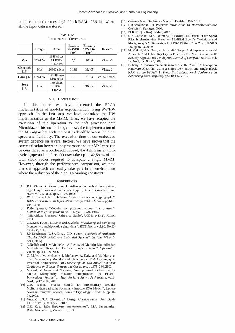
The proposed embedded system contains the following
components: Microblaze processor, memory BRAM, Local
Memory Bus (LMB), Processor Local Bus (PLB), Universal
Asynchronous Receiver Transmitter (UART), Timer and our
accelerator MM core. This latter communicates with the
processor via the memory-mapped-registrer [14].
Recent Advances in Electrical and Computer Engineering
ISBN: 978-1-61804-228-6 164

IP2 RFIFO_Data
WFIFO2IP_Data
WFIFO2IP_ RdAck
User_ Logic
Out_Slv_reg
MM Core
Read FIFO
IPIF
Instruction register
Bus2IP_clk
Out_Slv_reg(0)
Multiplier MonMul
Memory N
Memory Y
Memory X
Arithmetic Unit
32
N’
ControlUnit
N[j]S[j]i
Y[j]
X[i]
32
32
32
32 32
Write FIFO
Out_Slv_reg(31)
Out_Slv_reg(1)
FIFO
IPIC
W[j]i
PLB
Microblaze accesses either instruction through ILMB or
data through DLMB. These two buses are 32 bits. All the
peripherals communicate with the processor through the
PLB bus which is of 32 bits. The BRAM is configured to 16
KB memory space. The UART is integrated in the system to
allow the communication between the processor and the
RS232 port of the board. The Timer is used to gather
informations about how many clock cycles are required for
executing a single MMM and a modular exponentiation.
The device drivers of each peripheral are used to develop
the main program description which is executed by
Microblaze. Indeed, for computing single ME given by
M=PDmodN, Microblaze receives, as inputs from UART, the
exponent D, the message P, their sizes, the modulus, the
constant N' and the value of R2 mod N. Before performing
this function, the processor begins by restoring all the inputs
data according to their representation in radix 232
, then both
MMMs required for executing an iteration of the ME
algorithm, are calculated sequentially by the MM core. This
latter, receives the operands from the memory BRAM
through the processor, at each iteration of the modular
exponentiation algorithm. The MMM result will be then
transferred to the BRAM to be used as operand in next
computations. When the ME is achieved, the processor starts
by splitting the result M into 8-bits digits and sends it
outside FPGA via the UART; starting from least significant
digit to most significant digit.
The important component of our embedded system is the
designed MM core. In the following, let us consider its
implementation.
MM core Implementation
The integration of the MM core in the embedded system
requires not only the design of its hardware architecture and
an interface circuitry to communicate with the PLB bus, but
also the accompanied device drivers running on the
processor. The programs of these drivers are implemented
using the C code and designed on two layers. The first is the
high level driver. It consists of the ExpBinary(.) function
which allows to perform the modular exponentiation
algorithm. The second is the low level driver. It consists of
three functions Getbitindex(.), Write_Modulus_N'(.) and
Montgomery(.). Getbitindex(.) is executed by the processor.
Its role is to perform the right shift of the exponent D and
provide the (i)th
bit at the beginning of each iteration (i) of
the ME algorithm. Write_Modulus_N'(.) allows for
transmitting to MM core the modulus and the constant N’.
Montgomery(.) is used by Microbaze to ensure the
monitoring of the MMM computation. Except of the first
function, the others depend of the hardware interface
circuitry and allow the communication between the
processor and the MM core. Indeed, the process of making
the hardware interface can be time consuming task. Thus,
our work is based on using the IPIF (Intellectual Property
Interface) of Xilinx [15]. The block diagram of our
accelerator MM core based on a single Montgomery
modular multiplier is show in Fig. 3. It consists of the
interface IPIF and of the MonMul multiplier which can be
used as black box. This latter is responsible of the MMMs
execution. It mainly consists of: Memory data, our AU,
Control Unit and Memory FIFO. The IPIF uses a standard
back-end interface called IPIC (IP Interconnect) which helps
to connect our core to the IPIF services.
Fig. 3 Block diagram of the MM core
To allow the communication between Microblaze and the
multiplier MonMul, the internal components configured in
the interface IPIF are: Write FIFO, Read FIFO, and
instruction register. The write FIFO is used to transfer the
operands, the modulus and the constant N’ to MonMul. The
read FIFO ensures the reading of the result. The processor
controls the multiplier MonMul using instructions. These
latter are defined in the device drivers as opcodes and are
transmitted through the instruction register. Table I lists the
instructions and their opcodes.
TABLE I
INSTRUCTION FORMAT
Opcode Instruction Description
0000…..0001 Reset_MonMul
Initialization of the
multiplier MonMul after
each MMM execution
1000…..0001 Run_Write_N_N’ Loading the modulus N
and the constant N’
0000…..0000 Run_Write_X_Y Transferring two
operands to MonMul
0000…..0010 Run_MMM MMM execution
The signals of the IPIC are defined as follows:
Bus2IP_clk : Clock signal.
WFIFO2IP_data: Output data bus of the write FIFO.
WFIFO2IP_RdAck: Using an active high pulse, this
signal indicates, that a data on the WFIFO2IP_Data bus
is valid for reading at the next rising edge of the clock
signal. This pulse is a signal used inside the multiplier
MonMul, to control the loading of the input data into
local memories.
IP2RFIFO_data: Input data bus of the read FIFO.
Out_Slv_reg(31) and Out_Slv_reg(0): These signals are
the most significant and the least significant bits of the
instruction register, respectively. The first is used to
enable the loading of the modulus and the N’,
independently of both operands. The second allows the
initialization of the multiplier MonMul and enabling the
loading of two operands X and Y after performing each
MMM.
Recent Advances in Electrical and Computer Engineering
ISBN: 978-1-61804-228-6 165

Out_Slv_reg(1): This signal is the second bit of the
instruction register. It allows to active the execution of
the MMM arithmetic operations.
In order to perform the modular exponentiation, the
MonMul multiplier receives at each iteration two operands
namely, X and Y. According to the modular exponentiation
algorithm, X and Y can be the message P, the constant R2
mod N, or the intermediate results CCi and Sqi. Thus, for
performing one modular exponentiation, Microblaze starts
by sending first using the instruction “Run_Write_N_N’”, to
start the loading of the modulus and the constant N’. Then
the execution process becomes identical for all MMMs. The
basic operations for computing one MMM are as follows:
Before starting the MMM computation, Microblaze
transmits first the instruction “Run_Write_X_Y” to enable the
transfer of two operands X and Y which will be stored in
local memories. Once both operands are entirely received,
Microblaze sends the instruction ―Run_MMM” to start the
execution of the MMM. The transfer of the result from the
multiplier MonMul to Microblaze is based on the status of
the read FIFO link. During the transfer of data from
processor to MM core and when performing the MMM, this
link is high. In other words, the data bus IP2RFIFO_data
transmits 0xFFFFFFFF value to Microblaze. When the
multiplier MonMul completes the execution of one MMM, it
initializes the read FIFO by 0x00000000. After that, it sends
the (n+1) digits of the result. At the end, Microblaze
reinitializes the multiplier MonMul, using the instruction
―Reset_MonMul‖.
VI. IMPLEMENTATION RESULTS
The embedded system presented in this paper has been
designed by using Xilinx ISE design suite 13.2. To verify the
correctness of the MM core integration, functional
simulation was made using ModelSim SE 6.4 10.0C. The
architecture description of the multiplier MonMul was coded
using VHDL language. The memory blocks and DSP48E
cores were generated with the Core Generator tool of ISE.
The timing report showed that a maximum frequency
fmax=1/tclk of 100.26 Mhz can be achieved where tclk is the
clock period. This latter is computed from the AU critical
path, having the maximal delay. This delay corresponds to
the computation time of the products X[i]×Y[j] and q(i)×N[j]
which require one 32-bits multiplier.
Table II shows the execution time results, where the
proposed embedded system is clocked by 100 Mhz.
TABLE II
TEMPORAL PERFORMANCES
Bit width f
Mhz TMMM (ms) TModExp (ms)
short exponent 100 7171 10-5 2.6
Long exponent 100 7171 10-5 109.5
The encryption is applied for RSA 1024 bits with short
and long exponent. The short exponent is set to D=65537=
(10000000000000001)2. The long exponent is an integer
with 1024 bit-width. This sample has 515-bits non-zero
which is close and higher than the average case where the bit
string non-zero is about 512-bits.
In this table, TMMM and TModExp are the execution times of
a single MMM and of the modular exponentiation,
respectively. These times are computed by the multiplication
of the necessary clock cycles given by the Timer with the
clock period.
In this analysis, we are interested by the delay TModExp
which depends on several factors, namely: loading the
modulus and the constants N' into the MM core (T1);
executing a single MMM which includes the data transfer
(operands and result) between the processor and the MM
core (T2); shifting the exponent and testing its (i)th
bit (T3).
Finally, the TModExp depends also of number of bits equal to
zero in the exponent.
According to modular exponentiation algorithm, when
using short exponent D=65537, the complexity in terms of
number of MMMs and shifts is of (3×MMMs)+(17×(Shift
and test))+(19×MMMs). 3×MMMs are the MMMs required
to convert the execution of the modular exponentiation
algorithm in the Montgomery domain and to represent the
result in the classical domain. The results show that the first
three factors (T1, T2, and T3) required in terms of number of
clock cycles are 814, 7171 and 53, respectively. We note
that the number of clock cycles required for computing a
single MMM is high. Indeed, according to expression (13) of
section III, for RSA 1024 bits where the length of the data is
33 digits (n=32 bits), the execution of single MMM by our
AU requires only 1248 clock cycles instead of 7171. This
difference is mainly due to the data exchanged (operands
and result) between the processor and the MM core.
Precisely, the transfer of a single digit between the two parts
requires approximately 61 clock cycles. Thus, we can
consider that the communication between the processor and
our customized MM core can be seen as a bottleneck.
Table III shows the occupied resources by our embedded
system on the target FPGA circuit. These results are listed in
terms of number of slices, of select RAM blocks (36 kb
and18 kb) and of DSP48E cores. In order to evaluate the
costs of the MM core, we have implemented the basic
embedded system without our MM core. The result shows
that the difference is about 607 slices and 6 select RAM
blocks. In addition, the proposed Arithmetic Unit (AU) uses
11 DSP48E cores.
TABLE III OCCUPIED RESOURES
Slices Select RAM DSP48E
Our embedded system 1645 10 14
Basic embedded system 1038 4 3
MM core 607 6 11
Table IV compares our work with some previous
implementations of the modular exponentiation. Note that, in
the present work, our main goal is not the optimization of the
execution time, but to achieve the best trade-off between
area, speed and flexibility.
In [16], a hardware implementation of the modular
exponentiation is presented. This work is based on the
modified Booth encoder and on the carry save representation
to accelerate the MMM execution. In [17], the authors
present a SoC based on the Nios processor of Altera which
includes a variety of Intellectuals Property (RSA, ECC,…).
In this work, the modular exponentiation is implemented as
single core. In [18], a hardware implementation of the
Modular exponentiation is presented. This work promotes
the optimisation of the hardware resources, instead of the
execution time. In order to optimize the memory blocks
Recent Advances in Electrical and Computer Engineering
ISBN: 978-1-61804-228-6 166
number, the author uses single block RAM of 36kbits where
all the input data are stored.
TABLE IV
PERFORMANCES COMPARISON
Design Area TModExp
Z=65537
(ms)
TModExp
1024 bits
(ms)
Devices
Our SW/HW
1645 slices
14 DSPs
10 RAMs
2,6 109,6 Virtex-5
Ghoreishi
[16] HW 26640 slices 0.189 19.405 Virtex-2
Hani [17] SW/HW 12881(Logic
Elements) - 31,93 ep1s40f780c5
Song
[18] HW
180 slices
1 DSP
1 RAM
- 36.37 Virtex-5
VII. CONCLUSION
In this paper, we have presented the FPGA
implementation of modular exponentiation, using SW/HW
approach. In the first step, we have optimized the HW
implementation of the MMM. Then, we have adapted the
execution of this operation to the soft processor core
Microblaze. This methodology allows the implementation of
the ME algorithm with the best trade-off between the area,
speed and flexibility. The execution time of our embedded
system depends on several factors. We have shown that the
communication between the processor and our MM core can
be considered as a bottleneck. Indeed, the data transfer clock
cycles (operands and result) may take up to 82,59 % of the
total clock cycles required to compute a single MMM.
However, through the performances comparison, we note
that our approach can easily take part in an environment
where the reduction of the area is a binding constraint.
REFERENCES
[1] R.L. Rivest, A. Shamir, and L. Adleman,―A method for obtaining
digital signatures and public-key cryptosystems‖, Communication
ACM, vol 21, No.2, pp.120-126, 1978. [2] W. Diffie and M.E. Hellman, ―New directions in cryptography‖,
IEEE Transactions on Information Theory, vol.IT22, No.6, pp.644–
654, 1976. [3] P.Montgomery, ―Modular multiplication without trial division‖,
Mathematics of Computation, vol. 44, pp.519-521, 1985.
[4] ―MicroBlaze Processor Reference Guide‖, UG081 (v13.2), Xilinx, 2011.
[5] C.K.Koc, T.Acar, S.Burton and J.Kaliski , ―Analyzing and comparing
Montgomery multiplication algorithms‖, IEEE Micro, vol.16, No.33, pp.26-33,1996.
[6] J.P Deschamps, G.J.A Bioul, G.D. Sutter, ―Synthesis of Arithmetic
Circuits FPGA, ASIC, and Embedded Systems‖, (A John Wiley &
Sons, 2006).
[7] N.Nedjah and L.M.Mourelle, ―A Review of Modular Multiplication
Methods and Respective Hardware Implementation‖ Informatica, vol.30, pp.111-129, 2006.
[8] C. McIvor, M. McLoone, J. McCanny, A. Daly, and W. Marnane,
―Fast Montgomery Modular Multiplication and RSA Cryptographic Processor Architectures‖, In Proceedings of 37th Annual Asilomar
Conference on Signals, Systems and Computers, pp.379–384, 2003.
[9] M.Issad, M.Anane and N.Anane, ―An optimised architecture for radix-2 Montgomery modular multiplication on FPGA‖,
International Journal of High Perform System Architecture, vol.3,
No.4, pp.175-185, 2011. [10] C.D. Walter, ―Precise Bounds for Montgomery Modular
Multiplication and some Potentially Insecure RSA Moduli‖, Lecture
Notes in Computer Science,Topics in Cryptology - CT-RSA, pp.30–39, 2002.
[11] Virtex-5 FPGA XtremeDSP Design Considerations User Guide
UG193 (v3.5) January 26, 2012. [12] Ç.K. Koç, ―RSA Hardware Implementation‖, RSA Laboratories,
RSA Data Security, Version 1.0, 1995.
[13] Genesys Board Refference Manuall, Revision: Feb, 2012.
[14] P.R.Schaumont, ―A Practical Introduction to Hardware/Software
Codesign―, Springer, 2010. [15] PLB IPIF (v2.02a), DS448, 2005.
[16] S. S. Ghoreishi, M.A. Pourmina, H. Bozorgi, M. Dousti, ―High Speed
RSA Implementation Based on Modified Booth’s Technique and Montgomery’s Multiplication for FPGA Platform‖, In Proc. CENICS
'09, pp.86-93, 2009.
[17] M. K.Hani, H. Y. Wen, A. Paniandi, ―Design And Implementation Of A Private And Public Key Crypto Processor For Next Generation IT
Security Applications‖, Malaysian Journal of Computer Science, vol.
19, No 1, pp.29 – 45, 2006. [18] B. Song, K. Kawakami, K. Nakano and Y. Ito, ―An RSA Encryption
Hardware Algorithm using a single DSP Block and single Block
RAM on the FPGA‖, In Proc. First International Conference on Networking and Computing, pp.140-147, 2010.
Recent Advances in Electrical and Computer Engineering
ISBN: 978-1-61804-228-6 167