FPGA-Based High Performance AC DrivesFPGA-Based High Performance AC Drives (FPGA-basierte...
187
FAKULTÄT FÜR ELEKTROTECHNIK, INFORMATIK UND MATHEMATIK FPGA-Based High Performance AC Drives (FPGA-basierte Drehstromantriebe hoher Leistungsfähigkeit) Von der Fakultät für Elektrotechnik, Informatik und Mathematik der Universität Paderborn zur Erlangung des akademischen Grades Doktor der Ingenieurwissenschaften (Dr.-Ing.) genehmigte Dissertation von M.Sc. Shashidhar Mathapati Erster Gutachter: Prof. Dr.-Ing. Joachim Böcker Zweiter Gutachter: Prof. Dr.-Ing. Andreas Steimel Tag der mündlichen Prüfung: 28.03.2011 Paderborn, den 07.07.2011 Diss. EIM-E/275
Transcript of FPGA-Based High Performance AC DrivesFPGA-Based High Performance AC Drives (FPGA-basierte...

FAKULTÄT FÜRELEKTROTECHNIK,INFORMATIK UNDMATHEMATIK
FPGA-Based High Performance AC Drives
(FPGA-basierte Drehstromantriebe hoher Leistungsfähigkeit)
Von der Fakultät für Elektrotechnik, Informatik und Mathematik
der Universität Paderborn
zur Erlangung des akademischen Grades
Doktor der Ingenieurwissenschaften (Dr.-Ing.)
genehmigte Dissertation
von
M.Sc. Shashidhar Mathapati
Erster Gutachter: Prof. Dr.-Ing. Joachim BöckerZweiter Gutachter: Prof. Dr.-Ing. Andreas Steimel
Tag der mündlichen Prüfung: 28.03.2011
Paderborn, den 07.07.2011
Diss. EIM-E/275


Dedicated to late Prof. V.T. Ranganathan and
my brother late M.S. Kumar Swamy – Their short
association taught me uncountable lessons.


Acknowledgements
I sincerely thank my advisor Prof. Dr.-Ing. Joachim Böcker for providing me with an
opportunity to work in the field of Electrical Drives at the institute of Power Electronics
and Electrical Drives (LEA) Paderborn University. I am grateful for his generous support,
guidance and constructive engagement during the course of my stay at LEA.
I am grateful to Prof. Dr.-Ing. Andreas Steimel, head of the Institute for Electrical
Power Engineering and Power Electronics, Bochum University being he accepted to be
my co-advisor. My special thanks to him for his patient and very detailed corrections he
suggested while preparing the manuscript.
I am indebted to give my special thanks to Dr.-Ing. Norbert Fröhleke for being instru-
mental in introducing and bringing me into the motivated and friendly LEA group.
I owe a great deal to my colleagues at LEA for the many enlightening interactions, which
made my work possible and pleasant. In particular I am obliged to thank Mr. Schneider
for his valuable discussions and support he gave me while composing project proposals,
Mr. Romaus for all sorts of help he gave me during my stay in LEA, Mr. Knoke for his
humble domestic help being office-met and Mrs. Rittner for her bureaucratic help.
I unfeignedly thankful to Mr. Lönneker, Mr. Specht, Mr. W. Peters, Mr. Huber, Mr.
Figge, Mr. Grote, Mr. Dora, Mrs. Li, Mr. Schulte, Mr. Peter and Mr. Paradkar for
their humble support in correcting my presentations, papers and manuscript.
I am truly grateful to Mr. Foth, Mr. Sielemann and Mr Glunz who helped me in many
ways while working at my Laboratory test bench. My particular thanks are due to Mr.
W. Peters and Mr. Schulz for developing the FPGA based control platform, on which
most of my experiments are performed.
Paderborn, 28.03.2011
Shashidhar Mathapati

VII
Abstract
The state-of-the-art inverter used in standard and servo AC drives has a control system
with two processors. One of them is a microcontroller (MC), whose main job is to ac-
complish communication with the external world and the other is a DSP (digital signal
processor) core, responsible to carry out faster current-control or torque loop. These two
processors are memory-mapped for easy exchange of data. To accomplish control, current
and rotor position of the motor are necessary to be acquired. To get these information for
processing in the DSP, analog-to-digital converters (ADCs) and their associated interface
for communication are essential. The interfaces are usually implemented using discrete
ICs. The data converters (ADCs) are also external to the DSP; interfaced using serial
communication. Design engineers in drives industry like to keep the system untouched
for years, but unfortunately, modifications or upgrades in these discrete components or
products push the engineers to modify their system. In order to accomplish these hard-
ware modifications, the interfaces can be realized using re-programmable logic chips such
as PLDs (programmable logic device). However, PLDs have a very limited range of flexi-
bility and logic capabilities. The cost of the reprogrammable logic has reduced drastically
in this decade and along with it the density of logic functions on chip has increased
tremendously. These two factors helped the design engineers to think beyond these small
interface logic circuits resulting in FPGA entering the field of drive controls. In the near
future it is highly probable that FPGAs become the heart of inverter platform to run
the control algorithms. The motivation for this thesis is based on utilizing the potential
capabilities of FPGA optimally to address the open issues of drive control.
The control system running on a FPGA can easily be approximated as a continuous-time
system, due to its very small execution time. Based on this approach in the thesis a special
focus is given on analytical design procedure and performance enhancement of well-known
AC motor-control schemes (FOC, ISC and DTC). Also the efficient realization of data
acquisition systems based on ∆Σ-ADC, dynamically reconfigurable control for improving
the drive performance and fault-tolerance capabilities are addressed.


IX
Zusammenfassung
Moderne Stromrichter in Standard- und Servoantrieben werden überwiegend mit einem
digitalen System gesteuert und geregelt, das aus zwei Prozessoren besteht: Zum Einen
aus dem so genannten Mikrokontroller (MC), der die Kommunikation mit der Umge-
bung übernimmt, und zum Anderen aus dem digitalen Signalprozessor (DSP), der für
die schnellen Regelschleifen für Strom oder Drehmoment zuständig ist. Beide Prozes-
soren tauschen sich Daten über gemeinsame Speicherbereiche, das so genannte Memory-
Mapping, aus. Für die Regelung eines Antriebs sind die aktuellen Werte des Stromes und
der Rotorposition des Motors notwendig. Um diese Informationen zu erhalten, ist eine
Anbindung von Analog-Digital-Wandlern (ADCs) über ein geeignetes Interface an den
DSP wichtig. Dies wird meist mit diskreten ICs realisiert. Dabei werden die ADCs als
externe Bausteine über eine serielle Kommunikation mit dem DSP verbunden.
Entwickler in der Antriebstechnik würden dieses System gerne für Jahre unverändert
lassen. Veränderungen oder Aktualisierungen in den externen Bausteinen zwingen den
Entwickler jedoch zur Anpassung der Steuerungshardware. Diese Modifikationen kön-
nen durch die Verwendung von programmierbaren Logikbausteinen, wie z.B. PLDs (Pro-
grammable Logic Devices), realisiert werden. Diese PLDs haben einen eingeschränk-
ten Umfang an Flexibilität und Funktion. In der letzten Zeit sind die Kosten program-
mierbarer Bausteine drastisch gesunken, während deren Funktionsdichte enorm zugenom-
men hat. Diese beiden Faktoren eröffnen für den Systemdesigner die Möglichkeit, über
die beschriebenen Logikbausteine hinaus den Weg für die Einführung von FPGAs für
die Regelung von Antriebssystemen zu ebnen. In naher Zukunft ist es somit höchst
wahrscheinlich, dass FPGAs die Regelplattform für Umrichtersysteme bilden. Die Mo-
tivation dieser Arbeit ist die Untersuchung der optimalen Ausnutzung von FPGA zur
Lösung offener Fragestellungen in der Antriebsregelung.
Ein Regelungssystem, das mit einem FPGA realisiert wird, kann aufgrund seiner schnellen
Abarbeitungszeiten als ein zeitkontinuierliches System angesehen werden. Auf diesem
Ansatz basierend wird in dieser Arbeit ein Schwerpunkt auf den analytischen Entwurf
und die Eigenschaften bereits bekannter Regelverfahren für AC-Motoren (FOR, ISR und
DTC) gelegt. Eine effiziente Umsetzung eines Datenerfassungssystems mit ∆Σ-ADCs,
eine dynamisch konfigurierbare Regelung für die Verbesserung der Antriebseigenschaften
und die Fehlertoleranz des Systems werden ebenfalls betrachtet.


XI
Contents
Abbreviations and Symbols XV
1 Motivation and Organization of Thesis 1
2 Basics of FPGA 7
2.1 Memory types . . . . . . . . . . . . . . . . . . . . . . . . . . . . . . . . . . 7
2.1.1 Non-volatile memory . . . . . . . . . . . . . . . . . . . . . . . . . . 7
2.1.2 Volatile memory . . . . . . . . . . . . . . . . . . . . . . . . . . . . 9
2.2 History of programmable logic . . . . . . . . . . . . . . . . . . . . . . . . . 10
2.3 Initial FPGA architecture . . . . . . . . . . . . . . . . . . . . . . . . . . . 13
2.4 New-age FPGA . . . . . . . . . . . . . . . . . . . . . . . . . . . . . . . . . 15
2.4.1 Security issues of IP . . . . . . . . . . . . . . . . . . . . . . . . . . 15
2.4.2 Architecture . . . . . . . . . . . . . . . . . . . . . . . . . . . . . . . 17
2.5 Summary . . . . . . . . . . . . . . . . . . . . . . . . . . . . . . . . . . . . 22
3 Signal Processing Using FPGA 23
3.1 State of the art . . . . . . . . . . . . . . . . . . . . . . . . . . . . . . . . . 23
3.2 Unique features of FPGA . . . . . . . . . . . . . . . . . . . . . . . . . . . 24
3.3 Generic FPGA design methodology . . . . . . . . . . . . . . . . . . . . . . 25
3.4 Implementation of control algorithms on FPGA . . . . . . . . . . . . . . . 27
3.4.1 Bit-wise processing . . . . . . . . . . . . . . . . . . . . . . . . . . . 27
3.4.2 Word-wise processing . . . . . . . . . . . . . . . . . . . . . . . . . . 31
3.4.3 Development tools . . . . . . . . . . . . . . . . . . . . . . . . . . . 34
3.5 Summary . . . . . . . . . . . . . . . . . . . . . . . . . . . . . . . . . . . . 35
4 Analog-to-Digital Conversion Using Delta-Sigma (∆Σ) Modulator 37
4.1 Principle of analog-to-digital conversion . . . . . . . . . . . . . . . . . . . . 38
4.1.1 Basics of ADC . . . . . . . . . . . . . . . . . . . . . . . . . . . . . 39
4.1.2 Principle of oversampling . . . . . . . . . . . . . . . . . . . . . . . . 40
4.1.3 Nonlinear behavior of ∆Σ modulator . . . . . . . . . . . . . . . . . 44
4.2 Digital filters for noise attenuation . . . . . . . . . . . . . . . . . . . . . . 46
4.2.1 Cascaded integrator-comb filter . . . . . . . . . . . . . . . . . . . . 46
XII CONTENTS
4.2.2 IIR filters . . . . . . . . . . . . . . . . . . . . . . . . . . . . . . . . 55
4.2.3 Filter specification . . . . . . . . . . . . . . . . . . . . . . . . . . . 55
4.3 Implementation . . . . . . . . . . . . . . . . . . . . . . . . . . . . . . . . . 57
4.3.1 CIC with second-order sine compensation . . . . . . . . . . . . . . 57
4.3.2 IIR filter . . . . . . . . . . . . . . . . . . . . . . . . . . . . . . . . . 58
4.4 Experimental validation . . . . . . . . . . . . . . . . . . . . . . . . . . . . 61
4.5 Summary . . . . . . . . . . . . . . . . . . . . . . . . . . . . . . . . . . . . 65
5 Design of Pulse-Width-Modulation-based Motor Control on a FPGA 67
5.1 Field-oriented control . . . . . . . . . . . . . . . . . . . . . . . . . . . . . . 68
5.1.1 State-of-the-art FOC . . . . . . . . . . . . . . . . . . . . . . . . . . 69
5.1.2 Quasi-continuous control design . . . . . . . . . . . . . . . . . . . . 73
5.1.3 Implementation . . . . . . . . . . . . . . . . . . . . . . . . . . . . . 82
5.1.4 Experimental validation . . . . . . . . . . . . . . . . . . . . . . . . 85
5.1.5 Summary . . . . . . . . . . . . . . . . . . . . . . . . . . . . . . . . 89
5.2 Indirect Stator-quantity Control . . . . . . . . . . . . . . . . . . . . . . . . 90
5.2.1 State-of-the-art ISC . . . . . . . . . . . . . . . . . . . . . . . . . . . 90
5.2.2 Quasi-continuous control design . . . . . . . . . . . . . . . . . . . . 95
5.2.3 Implementation . . . . . . . . . . . . . . . . . . . . . . . . . . . . . 101
5.2.4 Experimental validation . . . . . . . . . . . . . . . . . . . . . . . . 103
5.2.5 Summary . . . . . . . . . . . . . . . . . . . . . . . . . . . . . . . . 105
6 Design of Direct Torque Control on a FPGA 107
6.1 Introduction . . . . . . . . . . . . . . . . . . . . . . . . . . . . . . . . . . . 107
6.2 Analytical analysis of DTC . . . . . . . . . . . . . . . . . . . . . . . . . . . 109
6.2.1 Basics of DTC . . . . . . . . . . . . . . . . . . . . . . . . . . . . . . 109
6.2.2 Detailed insight of DTC . . . . . . . . . . . . . . . . . . . . . . . . 111
6.3 Implementation . . . . . . . . . . . . . . . . . . . . . . . . . . . . . . . . . 123
6.4 Experimental validation . . . . . . . . . . . . . . . . . . . . . . . . . . . . 126
6.4.1 Comparison with PWM-based controls . . . . . . . . . . . . . . . . 129
6.5 Summary . . . . . . . . . . . . . . . . . . . . . . . . . . . . . . . . . . . . 131
7 Dynamically Reconfigurable Control Structures 133
7.1 Introduction . . . . . . . . . . . . . . . . . . . . . . . . . . . . . . . . . . . 133
7.2 Dynamic reconfiguration between high-performance control schemes . . . 137

CONTENTS XIII
7.2.1 Basic arrangement . . . . . . . . . . . . . . . . . . . . . . . . . . . 137
7.2.2 Implementation . . . . . . . . . . . . . . . . . . . . . . . . . . . . . 141
7.2.3 Experimental validation . . . . . . . . . . . . . . . . . . . . . . . . 145
7.3 Dynamic reconfiguration between a low-performance and a high-
performance control scheme . . . . . . . . . . . . . . . . . . . . . . . . . . 149
7.3.1 Basic arrangement . . . . . . . . . . . . . . . . . . . . . . . . . . . 149
7.3.2 Dynamically reconfigurable control structure . . . . . . . . . . . . . 151
7.3.3 Implementation . . . . . . . . . . . . . . . . . . . . . . . . . . . . . 153
7.3.4 Experimental validation . . . . . . . . . . . . . . . . . . . . . . . . 153
7.4 Summary . . . . . . . . . . . . . . . . . . . . . . . . . . . . . . . . . . . . 155
8 Conclusions 157
Bibliography 159
A Appendix 167
A.1 Test-bench arrangement . . . . . . . . . . . . . . . . . . . . . . . . . . . . 167
A.1.1 Motors . . . . . . . . . . . . . . . . . . . . . . . . . . . . . . . . . . 167
A.1.2 Converters and controllers . . . . . . . . . . . . . . . . . . . . . . . 168
A.2 Estimation of THD in DTC . . . . . . . . . . . . . . . . . . . . . . . . . . 169


XV
Abbreviations and Symbols
Characterized by style of writing
i(t), u(t), etc. instantaneous values
i(t), u(t), etc. complex time-variable vectors
i∗(t), u∗(t), etc. time-variable references
ix(t), ux(t), etc. complex vectors in special coordinates
i(t), u(t), etc. time derivative
I(s) = L(i(t)) etc. Laplace transforms
I(z) = Z(i(t)) etc. “z” transforms
Symbols
Abbreviation Variable Unit
C capacitance F
f frequency Hz
i current A
L inductance H
Pe noise spectral power W
R resistance Ω
T torque Nm
Ts sampling time s
u voltage V
ω angular velocity s-1
ǫ, θs, θr, δT angular coordinates
τ time constant s
ψ flux linkage Wb=Vs
∝ proportional to
Indices
is stator current
ir rotor current
isd, isq stator current components in d/q coordinates
isx, isy stator current components in x/y coordinates
ωrs mechanical speed
ω2 slip speed

XVI CONTENTS
Short-forms
ADC analog to digital converter
ASIC application specific integrated circuit
CIC cascaded integrator-comb
CLB configurable logic block
CMOS complimentary metal oxide semiconductor
CPLD complex PLD
DFOC direct field-oriented control
DSC direct self control
DSP digital signal processor
DTC direct torque control
e.g. for example
EMF electromotive force
ENOB effective number of bits
EPROM erasable programmable read only memory
E2PROM electrically erasable programmable read only memory
FIR finite impulse response
FPGA field programmable gate array
FOC field-oriented control
FTC fault-tolerant control
IIR infinite impulse response
IM induction machine
IP intellectual property
ISC indirect stator-quantity control
LC logic cell
LSB least significant bit
MAC multiply and accumulate
MC microcontroller
MSB most significant bit
OSR over sampling ratio
PI proportional-integral control
PLD programmable logic device
PMSM permanent-magnet synchronous machine
PWM/SVM pulse-width modulation/space-vector modulation
SAR successive approximation register
SRAM static read-only memory
SSI serial synchronous interface
S/H sample and hold
THD total harmonic distortion
viz. as follows
v/f voltage to frequency ratio

1
1 Motivation and Organization of Thesis
Electrical drives have an important role in electromechanical energy conversion, commonly
employed in transportation, material handling and most industrial production processes.
The increased user demand with respect to dynamic response, precision and flexibility
forced by technological advancement and energy conservation call for enhanced control.
During the period of the 1970s and 1980s, controlled electrical drives have explored rapid
market share due to greater innovations in semiconductor and microelectronics industry
in the form of efficient power-electronic devices and digital signal processors. Introduction
of controlled solid-state power converters have renewed variable-speed AC motor drives,
which are free from the drawbacks of mechanically commutated DC drives which domi-
nated the market for more than a century. Control of AC motor drives has created new
and difficult control problems, because the mechanically simpler AC machine is actually
a complex control plant in comparison to the DC machine. The course of development
of different types of AC motor control algorithms has contributed strongly to the field of
control engineering.
Early days of variable-speed AC motor drives can be recorded back to the 1960s, supplied
by variable-frequency inverters based on the silicon controlled rectifier (SCR). In that time
the principle of speed control was based on steady-state considerations mostly limited
to induction machine. The v/f (constant voltage to frequency ratio) control was one
outcome and even today it is commonly used for the open-loop speed control of drives
with low dynamic requirement. Along with that, another control technique was the slip-
frequency control method, which was well known to yield better dynamics. This method
was adopted in all high performance induction machine drives, until field-oriented control
(FOC) became the industry’s standard for AC drives with dynamics equal to DC motor
drives. Vector control or field-oriented control was one of the most important innovations
in AC motor drives, forced researchers to think beyond limits, which consequently resulted
in many new control schemes such as Direct Torque Control (DTC), Direct Self Control
(DSC) etc..
The inverter which converts the DC voltage into variable-frequency AC voltage is the
integral part of any AC drive system. The state-of-the-art inverter used in standard
and servo AC drives has a structure similar to that shown in Fig. 1.1. From the block
diagram it is understandable that the control system is made up of two processors. One
of them is the microcontroller (MC), whose main job is to accomplish communication
with the external world; this can be a simple display with keypad or a personal computer
(PC) or a Fieldbus system (CAN, SERCOS-III or EtherCAT). It is also responsible for
computing the slow-running control algorithms such as speed and flux control loops. The
other processor is the DSP (digital signal processor) core, responsible to carry out the
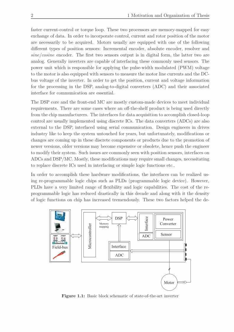
2 1 Motivation and Organization of Thesis
faster current-control or torque loop. These two processors are memory-mapped for easy
exchange of data. In order to incorporate control, current and rotor position of the motor
are necessarily to be acquired. Motors usually are equipped with one of the following
different types of position sensors: Incremental encoder, absolute encoder, resolver and
sine/cosine encoder. The first two sensors output is in digital form, the latter two are
analog. Generally inverters are capable of interfacing these commonly used sensors. The
power unit which is responsible for applying the pulse-width modulated (PWM) voltage
to the motor is also equipped with sensors to measure the motor line currents and the DC-
bus voltage of the inverter. In order to get the position, current and voltage information
for the processing in the DSP, analog-to-digital converters (ADC) and their associated
interface for communication are essential.
The DSP core and the front-end MC are mostly custom-made devices to meet individual
requirements. There are some cases where an off-the-shelf product is being used directly
from the chip manufacturers. The interfaces for data acquisition to accomplish closed-loop
control are usually implemented using discrete ICs. The data converters (ADCs) are also
external to the DSP, interfaced using serial communication. Design engineers in drives
industry like to keep the system untouched for years, but unfortunately, modifications or
changes are coming up in these discrete components or products due to the promotion of
newer versions, older versions may become expensive or obsolete, hence push the engineer
to modify their system. Such issues are commonly seen with position sensors, interfaces on
ADCs and DSP/MC. Mostly, these modifications may require small changes, necessitating
to replace discrete ICs used in interfacing or simple logic functions etc..
In order to accomplish these hardware modifications, the interfaces can be realized us-
ing re-programmable logic chips such as PLDs (programmable logic device). However,
PLDs have a very limited range of flexibility and logic capabilities. The cost of the re-
programmable logic has reduced drastically in this decade and along with it the density
of logic functions on chip has increased tremendously. These two factors helped the de-
Mic
roco
ntr
oll
er
PowerConverter
DSP
ADC
Sensor
Inte
rfac
e
Motor
ADC
Interface
Memorymapping
Field-bus
Figure 1.1: Basic block schematic of state-of-the-art inverter
3
sign engineers to think beyond these small interface logic circuits, the result of which
is the FPGA entering into the field of drive controls. The FPGA (field programmable
gate array) is the present-day popular re-programmable hardware logic. It offers greater
flexibility from the logic complexity and development point of view. Due to falling prices
for these hardware programmable logics, it makes sense to think of using them for more
than the simple interface logic circuits. First thing is to include faster control loops to be
computed by FPGAs, which implies that the control loops running in the DSP can now
be realized in the FPGA. This will yield specific advantages to the controller, because
the FPGAs offers true parallel processing capabilities, which eliminate the issue of the
computational delay that is associated with the sequentially executing DSP.
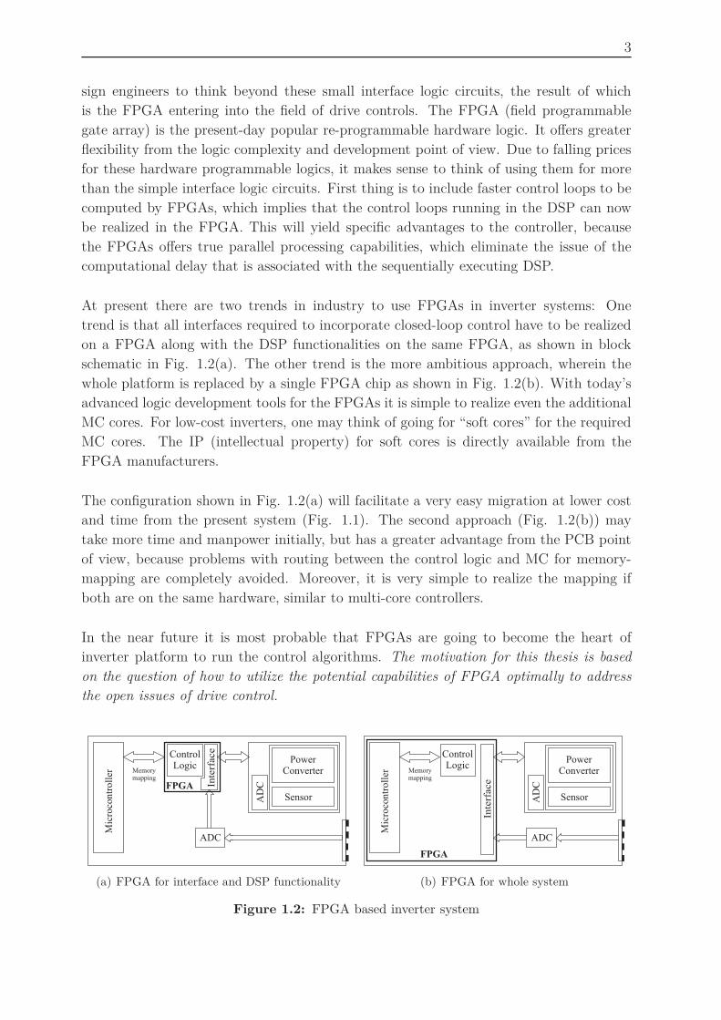
At present there are two trends in industry to use FPGAs in inverter systems: One
trend is that all interfaces required to incorporate closed-loop control have to be realized
on a FPGA along with the DSP functionalities on the same FPGA, as shown in block
schematic in Fig. 1.2(a). The other trend is the more ambitious approach, wherein the
whole platform is replaced by a single FPGA chip as shown in Fig. 1.2(b). With today’s
advanced logic development tools for the FPGAs it is simple to realize even the additional
MC cores. For low-cost inverters, one may think of going for “soft cores” for the required
MC cores. The IP (intellectual property) for soft cores is directly available from the
FPGA manufacturers.
The configuration shown in Fig. 1.2(a) will facilitate a very easy migration at lower cost
and time from the present system (Fig. 1.1). The second approach (Fig. 1.2(b)) may
take more time and manpower initially, but has a greater advantage from the PCB point
of view, because problems with routing between the control logic and MC for memory-
mapping are completely avoided. Moreover, it is very simple to realize the mapping if
both are on the same hardware, similar to multi-core controllers.
In the near future it is most probable that FPGAs are going to become the heart of
inverter platform to run the control algorithms. The motivation for this thesis is based
on the question of how to utilize the potential capabilities of FPGA optimally to address
the open issues of drive control.
Mic
roco
ntr
oll
er
PowerConverter
ADC
SensorAD
C
Memorymapping
ControlLogic
FPGA Inte
rface
(a) FPGA for interface and DSP functionality
Mic
roco
ntr
oll
er
PowerConverter
ADC
SensorAD
C
Memorymapping
FPGA
Inte
rface
ControlLogic
(b) FPGA for whole system
Figure 1.2: FPGA based inverter system
4 1 Motivation and Organization of Thesis
FPGAs in a broader spectrum are classified as memory. In order to understand the devel-
opment which has happened in the field of memory and how they have been used for pro-
grammable logic, a brief survey is given in chapter 2. Historically, the first programmable
logic which was used can be traced to simple memories such as the PROM (programmable
read-only memory). The course of technological development of programmable logic,
which emerged from simple PROMs to today’s advanced FPGA technology, is covered in
this chapter. The initial FPGA architecture was very primitive and used only for simple
“glue-logic” functions. This chapter also covers the evolution in the FPGA architecture to
meet the high-end complex logic functionalities with the necessary speed. The present-day
FPGA chips are more than just the programmable logic. They have embedded hardwired
hardware units to support the variety of signal-processing requirement. As these devices
became very advanced signal-processing and computing “power houses”, the big issue of
IP (intellectual property) security has arisen. More details on these versatile new FPGAs
regarding architecture and IP issues are also briefed in this chapter.
Algorithms used for control of electrical motors are multiplication and accumulation
(MAC) intensive. Signal-processing of these algorithms with sequentially-executing pro-
cessors is very well matured. Chapter 3 focuses on how the FPGAs capable of parallel
processing can be utilized here for realizing these algorithms efficiently. FPGAs give
greater liberty to the design engineer to develop his own approach of realizing the algo-
rithms to meet the space, resource and timing requirements. This chapter also briefs the
systematic generic design methodology of FPGAs.
Chapter 4 presents the idea to use 1-bit ADC instead of conventional multi-bit ADCs for
the motor control. The 1-bit ADC is referred to a ∆Σ modulator, they are the simplest
ADC from the construction and cheapest from the cost point of view. They are quite
commonly used in signal-processing applications specific to speech processing. The ∆Σ
ADC consists of two parts viz. modulator and filter; the modulator output is 1-bit data
with a high rate in the range of tens of MHz. This data stream is not serial word; actually
it is analog-converted equivalent 1-bit digital data along with high quantization noise. In
order to remove the quantization noise, a low-pass filter working at the same date rate
as the modulator is required. It is practically impossible to realize these filters on DSPs,
but with FPGAs it is feasible because they can easily be operated at a much higher rate
than the modulator. As this topic is new to the drives field, the theoretical background of
modulators is covered in this chapter. Unlike conventional multi-bit ADCs, the parameters
such as bandwidth and resolution for ∆Σ ADC can be controlled or programmed by an
appropriate design of filters. Hence a special focus on investigating different types of
filters is covered. Very popularly used SincK or CIC (cascaded integrator comb) filters
are discussed together with compensation techniques, FIR (finite impulse response) and
IIR (infinite impulse response) type filters are also discussed for possible application.
Detailed performance comparison relevant to drives applications and their feasibility of
FPGA implementation are presented with detailed experimental demonstration.
Chapter 5 presents the design criteria and procedures for the pulse-width modulation
(PWM) controllers realized on a FPGA. PWM-based controls such as FOC and Indi-

5
rect Stator-quantity Control (ISC), also known as PWM-DTC, are usually realized on a
DSP. The design principle is based on the well-known regular-sampled approach. With
this state-of-the-art approach, the dead-time introduced by the computational delay and
sampling restricts the achievable bandwidth of these controller. But, in this approach the
designer has the liberty to consider the PWM as a constant gain in control design. In
contrast, the controllers realized on FPGAs have very small computational delay, which
can be approximated close to continuous-time (quasi-continuous). A similar approxima-
tion of PWM as a constant gain allows to have infinite gain in the controller, implying
infinite bandwidth. A constant gain PWM model in the control is thus no more a valid
assumption for the quasi-continuous control. In order to address the criteria and the
procedure for the quasi-continuous design, a detailed investigation is carried out, an an-
alytical approach for the design is presented in this chapter. For the investigations, FOC
and ISC for a permanent-magnet synchronous machine (PMSM) with surface-mounted
magnets are considered. This chapter also emphasizes on how to achieve higher dynamics
with these controls without increasing the inverter switching frequency.
Chapter 6 presents a strategy for optimal hysteresis-band selection of DTC. The strategy
developed is based on the assumption of continuous-time control realization, which is
true in case of FPGA-based implementations. The strategy is completely offline and
analytical, to find out the adaptive hysteresis bands as a function of the operating point.
The selected bands are referred to as optimal, because they ensure the inverter switching
frequency to be constant, and they produce the minimum possible harmonic distortion in
the motor currents throughout the operating region. In this chapter, a detailed comparison
of dynamic performance of quasi-continuous PWM control (discussed in chapter 5) and
quasi-continuous DTC is also covered.
Lastly, in chapter 7 it is outlined how the FPGA can be utilized efficiently to implement re-
configurable structures. Reconfigurable structures are commonly known in fault-tolerant
control systems. In this chapter a generalized reconfigurable structure for electrical drives
is presented. It consists of more than one control scheme and facilitates the dynamic
change-over between the control schemes. The objective of such a reconfigurable struc-
ture is to enhance the control performance and the fault tolerance capability in the whole
operating region. An additional supervisory system is essential for the identification of the
fault to enable the reconfiguration. This chapter mainly emphasizes the generalized con-
cept of dynamic reconfiguration and its experimental demonstration under worst possible
operating conditions.

7
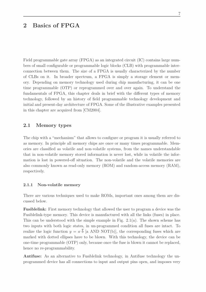
2 Basics of FPGA
Field programmable gate array (FPGA) as an integrated circuit (IC) contains large num-
bers of small configurable or programmable logic blocks (CLB) with programmable inter-
connection between them. The size of a FPGA is usually characterized by the number
of CLBs on it. In broader spectrum, a FPGA is simply a storage element or mem-
ory. Depending on memory technology used during chip manufacturing, it can be one
time programmable (OTP) or reprogrammed over and over again. To understand the
fundamentals of FPGA, this chapter deals in brief with the different types of memory
technology, followed by an history of field programmable technology development and
initial and present-day architecture of FPGA. Some of the illustrative examples presented
in this chapter are acquired from [CM2004].
2.1 Memory types
The chip with a “mechanism” that allows to configure or program it is usually referred to
as memory. In principle all memory chips are once or many times programmable. Mem-
ories are classified as volatile and non-volatile systems, from the names understandable
that in non-volatile memory stored information is never lost, while in volatile the infor-
mation is lost in powered-off situation. The non-volatile and the volatile memories are
also commonly known as read-only memory (ROM) and random-access memory (RAM),
respectively.
2.1.1 Non-volatile memory
There are various techniques used to make ROMs, important ones among them are dis-
cussed below.
Fusiblelink: First memory technology that allowed the user to program a device was the
Fusiblelink-type memory. This device is manufactured with all the links (fuses) in place.
This can be understood with the simple example in Fig. 2.1(a). The shown scheme has
two inputs with both logic states, in un-programmed condition all fuses are intact. To
realize the logic function y = a·b [a AND NOT(b)], the corresponding fuses which are
marked with dotted ellipses have to be blown. With this technology, the device can be
one-time programmable (OTP) only, because once the fuse is blown it cannot be replaced,
hence no re-programmability.
Antifuse: As an alternative to Fusiblelink technology, in Antifuse technology the un-
programmed device has all connections to input and output pins open, and imposes very

8 2 Basics of FPGA
a
b
y
+5 V
(a) Fusiblelink technology
a
b
y
+5 V
(b) Antifuse technology
Figure 2.1: Fuse technologies
high impedance, as shown in Fig. 2.1(b). If one fuses the same as Fig. 2.1(a), in the
Antifuse case which is shown in Fig. 2.1(b), the output logic becomes y = a·b [NOT(a)
AND b]. Similar to above, this technology is also one-time programmable (OTP). An
Antifuse device uses amorphous silicon linkages between two metal plates. Under un-
programmed condition these impose very high resistance in the range of hundreds of
MΩ. With programming a particular element, a link will grow by converting insulating
amorphous silicon into a conducting polysilicon.
Both Fusiblelink and Antifuse technique have the permanent link after programming,
i.e. it is non-volatile in nature, usually referred to as programmable read-only memory
(PROM), generally represented as in Fig. 2.2(a). Normally a high signal on the row line
makes the transistor on and pulls the column line to zero. To represent the column line
as “high” in the programmed condition, the shown fuse has to be blown. Even though
the first commercially launched PROM from Harris Semiconductors back in the 1970 was
based on fuse-link, it has no scope in today’s memory systems due to its poor reliability.
The blown fuses have the tendency of regrowing. While, in comparison the Antifuse
technique is more rugged and still used in few memory applications
EPROM and E2PROM: To obtain re-programmable PROM devices, an alternative
technology called erasable programmable read-only memory (EPROM) came into exis-
tence. First time this device was introduced by Intel Corporation in 1971. An EPROM
transistor has the same basic transistor as shown in Fig. 2.2(a) with an addition of a
second polysilicon floating gate, separated by a layer of oxide. In un-programmed condi-
tion, the floating gate is uncharged and hence does not effect the normal operation. To
program, about 12 V is applied to the controlled gate and the drain terminal. This causes
the hard turn-on of the transistor because the electrons force their way through the oxide
layer to the floating gate. When the programming signal is removed, the negative charge
remains on the floating gate. This charge is very stable and remains more than a decade
in normal operating conditions. The stored charge on the floating gate distinguishes the
cells which have been programmed from the un-programmed ones. That implies these
cells can be used for storing data without a Fusiblelink or an Antifuse, shown in Fig.
2.2(b). In this case placing a row line (data word) will turn the transistor on and pulls
the column line to zero.

2.1 Memory types 9
EPROM devices are considerably smaller and more efficient in silicon usage compared to
fuse devices. The main advantage is that the device can be erased and re-programmed.
An EPROM cell is erased by discharging the charge from the floating gate. The energy
required to discharge is given by an external ultraviolet radiation. These devices have
been supplied with ceramic or plastic packs with small quartz window open on the top.
Usually after programming, this window is covered with an opaque covering to avoid the
data loss.
Word line (row)D
ata
line
(colo
m)
+5 V
(a) Fusiblelink PROM
Word line (row)
Dat
a li
ne
(co
lom
)
EPROMtransistor
+5 V
(b) EPROM
Figure 2.2: PROM and EPROM
The main drawbacks of the EPROM have been the expensive quartz window and the
longer time of erasing. In order to overcome these problems, electrically erasable PROM
(E2PROM) have been introduced. They are similar to EPROM in principle, having
a similar floating gate, but with a thinner oxide layer around them, and an additional
transistor is used to erase the charge on the floating gate. Due to the additional transistor
the space and the silicon consumption is almost double that of the EPROM. EPROM and
E2PROM both were initially applied in the computer memory storage, but started later
to be employed as a programmable logic device (PLD), becoming erasable PLD and
electrically erasable PLD respectively.
Flash: The development of Flash Memory technology has its roots in EPROMs and
E2PROMs. The name Flash has originally been given because of its high-speed erasable
property compared to EPROMs. Devices based on Flash technology can have different
architectures. Some have single floating-gate-type transistors like in EPROM with thinner
oxide layer like in E2PROM. These devices can be electrically erasable, but only by clearing
the whole device or most of it. Another architecture is based on two transistors like in a
E2PROM, wherein it allows to erase and re-program the device word by word.
2.1.2 Volatile memory
There are two main versions of the semiconductor RAM, the dynamic RAM (DRAM)
and the static RAM (SRAM). In case of DRAM, each cell is made of transistor-capacitor
pairs, consuming very little silicon. A dynamic qualifier is used, because capacitors loose
their charge with time, hence each cell has to be recharged periodically to make sure data
is not lost. This process is known as “refreshing”, which is indeed complex and requires
10 2 Basics of FPGA
additional circuitry. Especially with big storage devices, DRAM technology works out
very cost effective. Yet the DRAM technology is not attractive for the programmable
logic.
In case of SRAM devices, once a value is loaded it will not change unless the value itself
is altered or power is turned off. A SRAM cell consists of multi transistors to drive the
output control transistor. Depending on the storage information, the output transistor
will be either “on” or “off”. One major disadvantage of a SRAM-based programmable
device is that they consume a significant area of silicon, because these cells are made up
of four to six transistors. Another disadvantage stems from the inherent volatile nature,
as the data is lost with power-off situation, which implies that they require every time
programming with power on. However, these devices can be programmed reasonably fast
and as many times as required.
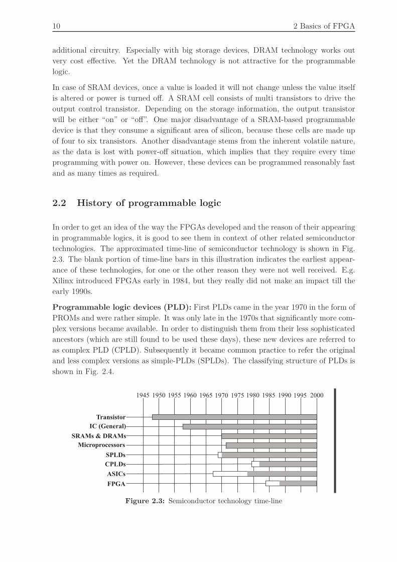
2.2 History of programmable logic
In order to get an idea of the way the FPGAs developed and the reason of their appearing
in programmable logics, it is good to see them in context of other related semiconductor
technologies. The approximated time-line of semiconductor technology is shown in Fig.
2.3. The blank portion of time-line bars in this illustration indicates the earliest appear-
ance of these technologies, for one or the other reason they were not well received. E.g.
Xilinx introduced FPGAs early in 1984, but they really did not make an impact till the
early 1990s.
Programmable logic devices (PLD): First PLDs came in the year 1970 in the form of
PROMs and were rather simple. It was only late in the 1970s that significantly more com-
plex versions became available. In order to distinguish them from their less sophisticated
ancestors (which are still found to be used these days), these new devices are referred to
as complex PLD (CPLD). Subsequently it became common practice to refer the original
and less complex versions as simple-PLDs (SPLDs). The classifying structure of PLDs is
shown in Fig. 2.4.
1945 1950 1955 1960 1965 1970 1975 1980 1985 1990 1995 2000
Transistor
IC (General)
SRAMs & DRAMs
Microprocessors
SPLDs
CPLDs
ASICs
FPGA
Figure 2.3: Semiconductor technology time-line
2.2 History of programmable logic 11
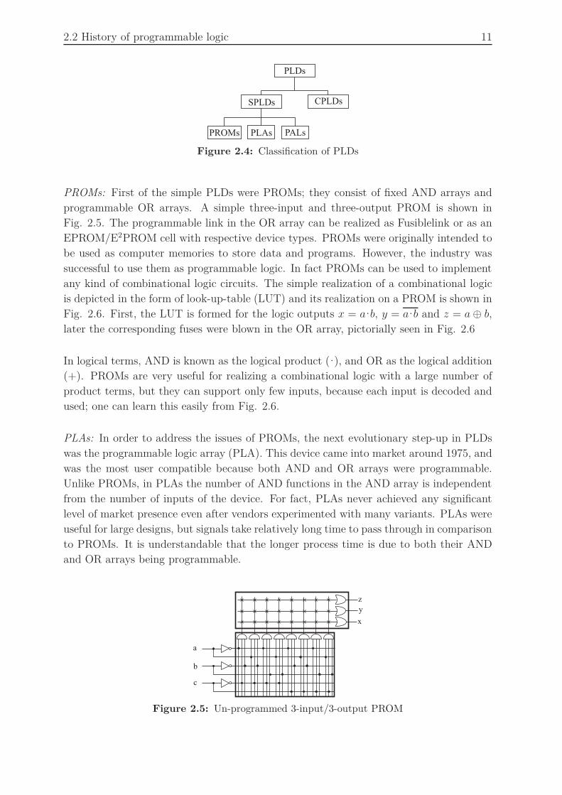
PLDs
CPLDsSPLDs
PROMs PLAs PALs
Figure 2.4: Classification of PLDs
PROMs: First of the simple PLDs were PROMs; they consist of fixed AND arrays and
programmable OR arrays. A simple three-input and three-output PROM is shown in
Fig. 2.5. The programmable link in the OR array can be realized as Fusiblelink or as an
EPROM/E2PROM cell with respective device types. PROMs were originally intended to
be used as computer memories to store data and programs. However, the industry was
successful to use them as programmable logic. In fact PROMs can be used to implement
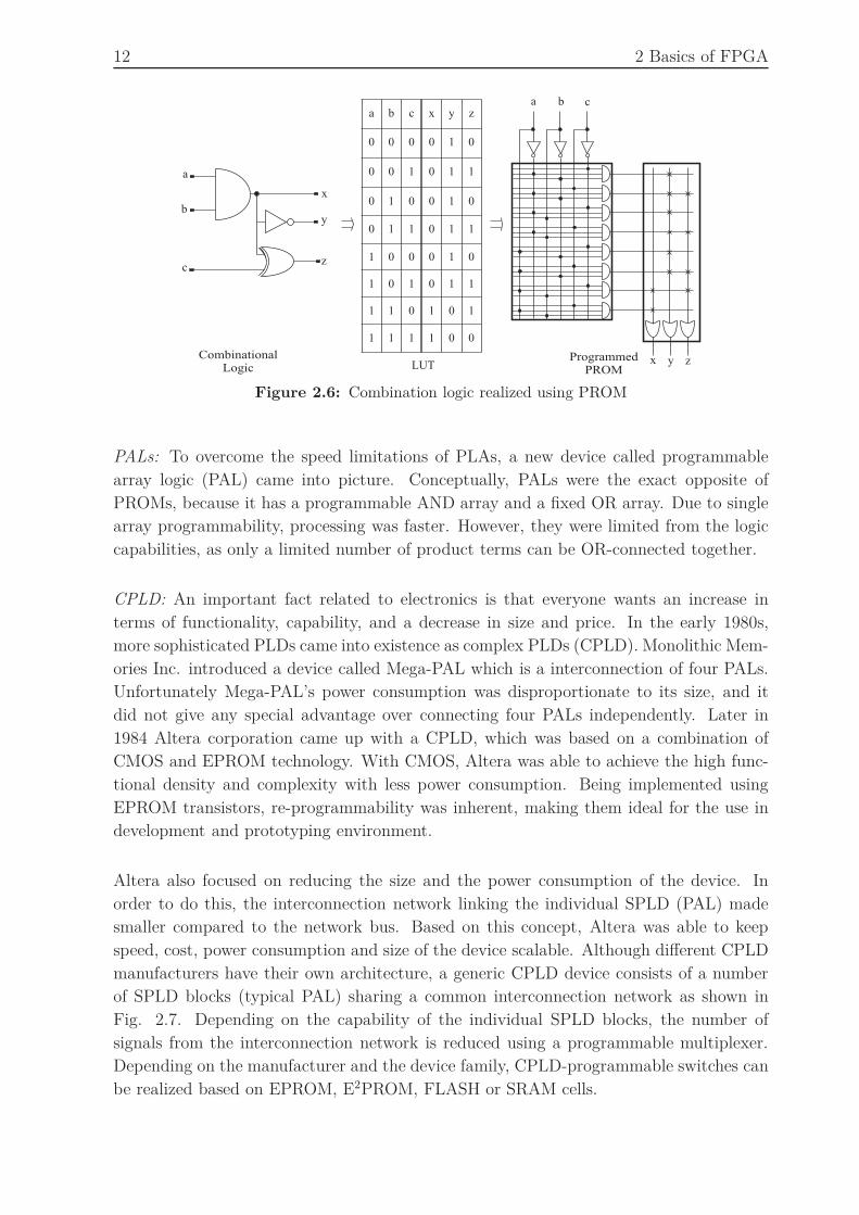
any kind of combinational logic circuits. The simple realization of a combinational logic
is depicted in the form of look-up-table (LUT) and its realization on a PROM is shown in
Fig. 2.6. First, the LUT is formed for the logic outputs x = a·b, y = a·b and z = a⊕ b,
later the corresponding fuses were blown in the OR array, pictorially seen in Fig. 2.6
In logical terms, AND is known as the logical product (·), and OR as the logical addition
(+). PROMs are very useful for realizing a combinational logic with a large number of
product terms, but they can support only few inputs, because each input is decoded and
used; one can learn this easily from Fig. 2.6.
PLAs: In order to address the issues of PROMs, the next evolutionary step-up in PLDs
was the programmable logic array (PLA). This device came into market around 1975, and
was the most user compatible because both AND and OR arrays were programmable.
Unlike PROMs, in PLAs the number of AND functions in the AND array is independent
from the number of inputs of the device. For fact, PLAs never achieved any significant
level of market presence even after vendors experimented with many variants. PLAs were
useful for large designs, but signals take relatively long time to pass through in comparison
to PROMs. It is understandable that the longer process time is due to both their AND
and OR arrays being programmable.
a
b
c
x
y
z
Figure 2.5: Un-programmed 3-input/3-output PROM
12 2 Basics of FPGA
a b c
x y z
a b c x y z
0 0 0 0 1 0
0 0 1 0 1 1
0 1 0 0 1 0
0 1 1 0 1 1
1 0 0 0 1 0
1 0 1 0 1 1
1 1 0 1 0 1
1 1 1 1 0 0
a
b
c
x
y
z
LUTProgrammed
PROM
CombinationalLogic
Figure 2.6: Combination logic realized using PROM
PALs: To overcome the speed limitations of PLAs, a new device called programmable
array logic (PAL) came into picture. Conceptually, PALs were the exact opposite of
PROMs, because it has a programmable AND array and a fixed OR array. Due to single
array programmability, processing was faster. However, they were limited from the logic
capabilities, as only a limited number of product terms can be OR-connected together.
CPLD: An important fact related to electronics is that everyone wants an increase in
terms of functionality, capability, and a decrease in size and price. In the early 1980s,
more sophisticated PLDs came into existence as complex PLDs (CPLD). Monolithic Mem-
ories Inc. introduced a device called Mega-PAL which is a interconnection of four PALs.
Unfortunately Mega-PAL’s power consumption was disproportionate to its size, and it
did not give any special advantage over connecting four PALs independently. Later in
1984 Altera corporation came up with a CPLD, which was based on a combination of
CMOS and EPROM technology. With CMOS, Altera was able to achieve the high func-
tional density and complexity with less power consumption. Being implemented using
EPROM transistors, re-programmability was inherent, making them ideal for the use in
development and prototyping environment.
Altera also focused on reducing the size and the power consumption of the device. In
order to do this, the interconnection network linking the individual SPLD (PAL) made
smaller compared to the network bus. Based on this concept, Altera was able to keep
speed, cost, power consumption and size of the device scalable. Although different CPLD
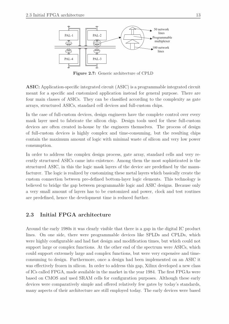
manufacturers have their own architecture, a generic CPLD device consists of a number
of SPLD blocks (typical PAL) sharing a common interconnection network as shown in
Fig. 2.7. Depending on the capability of the individual SPLD blocks, the number of
signals from the interconnection network is reduced using a programmable multiplexer.
Depending on the manufacturer and the device family, CPLD-programmable switches can
be realized based on EPROM, E2PROM, FLASH or SRAM cells.
2.3 Initial FPGA architecture 13
PAL-1 PAL-2
PAL-3PAL-4
Programmablemultiplexer
100 networklines
50 networklines
Figure 2.7: Generic architecture of CPLD
ASIC: Application-specific integrated circuit (ASIC) is a programmable integrated circuit
meant for a specific and customized application instead for general purpose. There are
four main classes of ASICs. They can be classified according to the complexity as gate
arrays, structured ASICs, standard cell devices and full-custom chips.
In the case of full-custom devices, design engineers have the complete control over every
mask layer used to fabricate the silicon chip. Design tools used for these full-custom
devices are often created in-house by the engineers themselves. The process of design
of full-custom devices is highly complex and time-consuming, but the resulting chips
contain the maximum amount of logic with minimal waste of silicon and very low power
consumption.
In order to address the complex design process, gate array, standard cells and very re-
cently structured ASICs came into existence. Among them the most sophisticated is the
structured ASIC, in this the logic mask layers of the device are predefined by the manu-
facturer. The logic is realized by customizing these metal layers which basically create the
custom connection between pre-defined bottom-layer logic elements. This technology is
believed to bridge the gap between programmable logic and ASIC designs. Because only
a very small amount of layers has to be customized and power, clock and test routines
are predefined, hence the development time is reduced further.
2.3 Initial FPGA architecture
Around the early 1980s it was clearly visible that there is a gap in the digital IC product
lines. On one side, there were programmable devices like SPLDs and CPLDs, which
were highly configurable and had fast design and modification times, but which could not
support large or complex functions. At the other end of the spectrum were ASICs, which
could support extremely large and complex functions, but were very expensive and time-
consuming to design. Furthermore, once a design had been implemented on an ASIC it
was effectively frozen in silicon. In order to address this gap, Xilinx developed a new class
of ICs called FPGA, made available in the market in the year 1984. The first FPGAs were
based on CMOS and used SRAM cells for configuration purposes. Although these early
devices were comparatively simple and offered relatively few gates by today’s standards,
many aspects of their architecture are still employed today. The early devices were based

14 2 Basics of FPGA
3 inputLUT
mux
flip-flop
y
q
a
bc
d
clock
Figure 2.8: Initial structure of logic block
on the concept of a programmable logic block, which comprised a 3-input lookup table
(LUT), a register that could act as a flip-flop or a latch and a multiplexer. Fig. 2.8 shows a
very simple programmable logic block, each FPGA contains large number of these blocks.
By means of SRAM programming cells, each logic block in the device could be configured
to perform a different function. Each register could be configured to initialize containing
a logic 0 or a logic 1 and to act as a flip-flop or a latch. If the flip-flop option was selected,
the register could be configured to be triggered by a positive- or a negative-going clock
(the clock signal was common to all of the logic blocks). The multiplexer feeding the
flip-flop can be configured to accept the output of the LUT or a separate input to the
logic block. The LUT can be configured to represent any 3-input logical function.
ConfigurableInput/Output Block
ConfigurableLogic Block Programmable
interconnection
Figure 2.9: General structure of FPGA
The FPGA comprises a large number of these programmable logic blocks surrounded
by a number of programmable interconnects shown in Fig. 2.9, which is an abstract
representation of a FPGA. In reality, all transistors and interconnects are implemented
on the same piece of silicon using standard IC creation technique. The device also includes
primary I/O pins and pads. With help of its own SRAM cells, the interconnects could be
programmed such that the primary inputs of the device were connected to the inputs of
one or more programmable logic blocks, and the outputs from any logic block could be
used to drive the inputs of any other logic block.
With this novel architecture, FPGAs successfully bridged the gap between PLDs and
ASICs. On one hand, they were highly configurable and had the fast design and modifi-
cation times associated with PLDs, and on the other hand they can be used to implement
large and complex functions that had previously been the exclusive domain of ASICs.
2.4 New-age FPGA 15
2.4 New-age FPGA
Today, the majority of FPGAs is based on SRAM configuration cells. That implies the
device can be programmed and re-programmed. The main advantage of these devices
is that they are in the fore-front of technology. The companies specialized in memory
devices are expanding their research and development (R&D) in CMOS techniques. The
SRAM cells are created exactly using the same CMOS technology, so no special processing
steps are required to produce these devices. One important disadvantage with the SRAM
devices is, for each time “power on” the device has to be programmed. This requires the
use of an external memory to store the configuration data, which adds cost and space.
2.4.1 Security issues of IP
Protection of intellectual property (IP) in the FPGA device is an important topic of
interest from the industrial revenue point of view. A FPGA design can take several months
to develop; if it is not protected adequately, it will be stolen in no time. Protecting IP
means preserving competition and protecting the investments.
Decision about which type of FPGA to use is a critical question in the overall system
protection. Different types of FPGAs provide a variety of security levels, but in general
non-volatile Antifuse and Flash devices are more secure compared to volatile SRAM-based
devices. This is because SRAM devices require an external configuration memory to store
the bit-file (configuration file), on power-up the bit-file is transferred to the FPGA for the
logic configuration. In an unprotected application, it is very simple to copy the content of
the external memory, enabling the proprietary IP to be cloned. Hence at the basic level
without any additional protection measures, the nonvolatile devices are more secure than
the volatile ones.
SRAM-based device: Along with the non-volatile characteristic of SRAM devices they
also lack in providing appropriate security for the IP. This is because the configuration file
which is used to program the device is kept in the external memory. Currently there are
no commercially available tools which can make the schematic out of these configuration
files. Understanding and extracting the logic from the configuration file is not a simple
and easy task, but not beyond the bound of possibility. If the design is highly profitable,
there are companies who are willing to replicate the IP. The main issue is not only stealing
the IP by “reverse engineering”, it is beyond that: Cloning the whole design or circuit
board.
Recognizing this, some of today’s FPGA manufacturers have implemented support for
bitstream encryption for SRAM-based devices. For these devices, the bitstream can be
encrypted using a triple data encryption standard (3DES) or comparable algorithms and
stored in an external memory. The encryption key is loaded on to a special SRAM-
based register in the FPGA via the JTAG port. In conjunction with some associated
logic, the key allows the decryption of the incoming encrypted configuration bitstream

16 2 Basics of FPGA
from the memory into the FPGA. The decrypted bitstream is mapped onto the FPGA.
The process of loading the encryption file automatically disables the FPGAs read-back
capability. While this makes impossible for all except the most sophisticated hackers
stealing and cloning the IP. The main drawback of this scheme is that you require a
battery back-up on the circuit board to maintain the content of the encryption key on
the FPGA. This battery will have decades of life-time, because it needs only to maintain
a single register. But it adds up to the size, complexity and cost of the board.
Antifuse-based device: Antifuse FPGAs are programmed off-line using a special device
programmer. The configuration file commonly known as fuse-map file is first loaded to
the device programmer and the programmer will decide which are the fuses to be pro-
grammed. Further, the programmer sends commands to the FPGA for mapping the logic.
This is a very basic difference to Antifuse and other variants of FPGA technologies, as
they use a bitstream for mapping. The inherent nonvolatile nature of these devices makes
them ready to use as the system is powered. Following from their non-volatility, these
devices do not require an external memory to store the configuration data, which saves
space on board and the cost for the additional device. One more very important advan-
tage of these devices is that the interconnect structure is naturally immune to radiation
(rad hard). This is of particular interest for military and aerospace applications. With
Antifuse FPGAs all of the “intelligence” is in the programmer, not in the device, so no
programming file (or bitstream) is readable from the device. This makes Antifuse FP-
GAs immune to cloning and also do security fuses, once programmed, disable the probe
and the programming interface on the device, hence further protecting against hackers.
From a practical perspective, Antifuse devices are impossible to clone. Designs developed
by industry and government requiring the highest degree of IP protection are usually
developed with Antifuse devices.
E2PROM/FLASH-based device: As no one produces EPROM-based FPGAs today,
we will restrict our discussion to E2PROM/Flash devices. Flash FPGAs offer all the IP
protection provided by Antifuse devices in terms of non-volatility and, having all memory
on-chip, are secured when locked. With a flash device, the application designer writes the
configuration bitstream into the device during manufacturing of the application and then
locks it the part, increasing the IP security of flash devices, because the configuration
bitstream is never exposed or available outside of the device where it can be obtained and
cloned. Unlike Antifuse devices, a flash FPGA contains the configuration bitstream, so
if the bitstream can be extracted from the part, the proprietary IP can be cloned. As
a result, flash FPGA manufacturers provide several levels of security locking circuits to
protect the proprietary content in the device. When a flash FPGA is locked, functions
such as device read, write, verify and erase are disabled. Unlike Antifuse, FLASH devices
allows re-programmability, in some applications this capability is highly desirable, but it
is in conflict with the ability to configure the device and then lock it to protect the IP. To
accommodate re-programmability and still enable the application designer to lock a flash
device, the first level of locking works via an user-defined key that the designer uses to

2.4 New-age FPGA 17
lock or unlock the device. Table 2.1 gives the summary and comparison of the different
FPGA process technologies.
2.4.2 Architecture
It is very common to categorize FPGAs as being either fine-grained or coarse-grained
devices. In order to understand what this means, we need to remember the main feature
that distinguishes FPGAs from other devices, i.e. they consist of large numbers of rela-
tively simple programmable logic blocks with programmable interconnections. In case of
fine-grained architecture, each logic block can be used to implement only a very simple
function. E.g. it might be the block to act as any 3-input function, such as a primitive
logic gate (AND, OR, NAND, etc.) or a storage element.
In addition to implementing glue logic and state machines, fine-grained architectures are
said to be efficient when executing systolic algorithms. These architectures are also said
to offer some advantages with regard to traditional logic synthesis technology, which is
more like fine-grained ASIC architectures. The middle 1990s saw a lot of interest in fine-
grained FPGA architectures, but over time the vast majority faded away, leaving only
the coarse-grained devices. In the case of a coarse-grained architecture, each logic block
contains a relatively large amount of logic, compared to the fine-grained devices. For
example, a logic block might contain four 4-input LUTs, four multiplexers, four D-type
flip-flops and some fast carry logic.
An important consideration with regard to architectural granularity is that fine-grained
implementations require a relatively large number of connections into and out of each
block, compared to the amount of functionality that can be supported by those blocks.
Table 2.1: Comparison of FPGA process technologies
SRAM E2PROM/Flash Antifuse
Technology State-of-the-art one or more one or more
generation behind generation behind
Re-programmable Yes Yes No
Programming speed Fast 3X slower –
to SRAM
Volatile Yes No No
External configuration Yes No No
Prototyping purpose Very good Reasonable No
Instant on No Yes Yes
IP Protection level good Very good Very good
Size of configuration cell Large Medium Very small
Power Consumption Medium Low Medium
Susceptibility to Unprotected Unprotected Protected
hard radiation

18 2 Basics of FPGA
As the granularity of the blocks increases to medium-grained and higher, the amount of
connections into the blocks decreases compared to the amount of functionality they can
support. This is important because the programmable interconnect accounts for the delays
associated with signals as they propagate through. There are two fundamental variants
of the programmable logic blocks used to form the medium-grained architectures: MUX-
(multiplexer) and LUT-based blocks.
MUX-based: As an example of a MUX-based approach, consider a function y = (a·b)+c,
which can be implemented using only multiplexers as shown in Fig. 2.10. The device can
be programmed such that each input to the block is presented with a logic 0 or 1, or the
input signals (a, b, or c in this case) or coming from another block. This allows each
block to be configured in many different ways, to incorporate the function.
LUT-based: The concept with LUT-based design is simpler, a group of input signals
is used as index to a look-up-table. The content of the table is arranged such that the
cell pointed by each input combination contains the desired value. For understanding,
lets consider the same case as discussed for the MUX-based design. This is achieved
with the 3-input LUT with the appropriate values evaluated from the truth table. One
can consider the LUT being formed from SRAM cells (could be done as well with the
other techniques Antifuse/EPROM/E2PROM/FLASH). The common practice is to use
the inputs to select the desired SRAM cell using cascaded gates for the transmission. Fig.
2.11 is self explanatory for the LUT logic function. If the transmission gate is enabled, the
signal seen on its input passes through to its output. If the gate is disabled, its output is
electrically disconnected from the wire it is driving. The transmission-gate symbol shown
with a small circle (commonly known as “bubble”) indicates that these gates are activated
with the logic zero, symbols without bubble indicate that these gates are activated by a
logic one.
During the initial days, engineers use to design their logic circuits in a “handicraft” man-
ner, unlike today’s sophisticated CAD tools. Some of those engineers always claimed
that MUX-based designs were the best suited to realize; however there was no conclusive
reason given for it. The MUX-based architectures do not provide the high-speed carry
logic chains which are very important to realize the arithmetic operations, in which the
0
1ab
c
001
0
0
1y
a
b
c
CLB
CLBCLB
CLBCLB
y = a·b+ c
Figure 2.10: Logic realization using multiplexer (MUX)

2.4 New-age FPGA 19
a
b
c
a b c y
0 0 0 1
0 0 1 0
0 1 0 1
0 1 1 0
1 0 0 1
1 0 1 0
1 1 0 1
1 1 1 1
Truth table
0
1
1
0
1
0
1
1
y
abc
Transmission gate(active low)
Transmission gate(active high)
y = a·b+ c
Figure 2.11: Logic realization using look-up-table (LUT)
LUT-based counterparts are far ahead. Throughout much of 1990s, FPGAs were widely
used in the telecommunication and networking markets. Both the applications involved
a lot of data processing, wherein the LUT-based architectures were more suitable. Fur-
thermore, as designs grew larger and synthesis technology improved with sophistication,
handicraft circuits became a thing of the past; as a result, the majority of today’s FPGAs
has only LUT-based architectures.
The unique thing about a n-input LUT is that it can implement any possible n-input
combinational logic function. Adding more inputs allows you to represent more complex
functions, but every addition of a single bit requires two additional SRAM cells. FPGA
manufacturers and the universities have done lot of research to find out the optimum bits
for the LUT in CLBs. Till early 2000, the FPGAs with 4-input-LUT-based architecture
was thought to be optimal, now very recently Xilinx has come up with 6-input-LUT-based
architecture claiming to be “more” optimum. It seems that it is not only the bits of the
LUT, also relevant is how these basic logic blocks are utilized to realize the number of
functionalities such as logic, arithmetic and memory functions.
In a SRAM-based FPGA, the n-bit LUT is made of 2n SRAM cells. These SRAM cells
offer a number of interesting possibilities. In addition to their primary role as LUT, they
can also be used as a small block of RAM (16 cells forming a 4-bit LUT can be used
as a 16X1 RAM). It is commonly referred to as distributed RAM, because LUTs are
distributed throughout the surface. Another possibility of these cells is that they can be
stringed together in a long chain to make them operate as shift registers (SR). Hence the
LUT is multifaceted, as shown in Fig. 2.12.
Configurable blocks: In order to have the most efficient realization of logic, the con-
figurable blocks do not only consist of LUTs, in addition they also have multiplexer and
register. A pity for the FPGA is each vendor has his own names and terminology for his

20 2 Basics of FPGA
4-input LUT
16X1 RAM
16-bit SR
Figure 2.12: Multifaceted LUT
architectural components. Xilinx and Altera are giants as FPGA vendors, hence in this
section only their products terminologies are used.
Formally, the very basic configurable block of Xilinx-based FPGA is called logic cell (LC),
which usually consists of a 4-input LUT; it can also be configured as 16X1 RAM or 16-bit
SR, a multiplexer and a register. Two LC use to make a Slice and four Slices together a
configurable logic block (CLB). The present architecture of the CLB has evolved from this
basic construct and the recent devices such as Spartan-6 and Vertex-6 are based on 6-input
LUTs. Consisting of two Slice per CLB and four 6-input LUT and 8-FF per Slice, in total
each CLB has 16 LUT and 32 FFs. The Slices are arranged in two columns for every CLB
column. For the efficient mapping, these devices also come with slightly modified Slices
to suit for memory and logic operations. Fig. 2.13 shows a simplified version of a CLB; it
also consists of some special carry logic for use in memory and arithmetic operations (CIN
and COUT). The Slices within the CLB are not communicating in-between themselves,
instead they are directly connected to the Switch Matrix.
From the architectural point, a logic element (LE) is the basic building block of Altera’s
FPGA which also has a similar structure as discussed above. Indeed there exists a lot of
differences when discussed at deeper level, but the overall structure shows the resemblance
to a LC. Altera’s configurable block is called logic array block (LAB) consisting of 16 LEs
based on 4-input LUT architecture.
slice 0
slice 1
Sw
itch
-Mat
rix
CIN
COUT
Figure 2.13: CLB of Spartan-6 FPGA
2.4 New-age FPGA 21
Embedded RAMs: A lot of applications requires the use of memory, hence FPGAs
come with large chunks of embedded RAM. They are also known as e-RAM or block-
RAM. Depending on the type of device, the block-RAM size can be anything between
few thousands to tens of thousands of bits. Further a device can contain tens to few
hundreds of these blocks. These blocks can be used independently or can be combined
together, to use it as a big memory. They can be used in a variety of purposes, a single-
port or a dual-port RAM, first-in-first-out (FIFO), state machine and so forth.
Embedded multipliers: Functions like multiplication, realized by connecting a number
of CLBs, makes the process very slow. As this function is required by most applications,
many FPGA manufacturers provide hardwired multipliers blocks. They are placed very
adjacent to the embedded RAM blocks. In some of the advanced and expensive FPGAs
the dedicated adder comes along with this embedded multiplier to provide the complete
MAC (multiply-and-accumulate) functionality. MAC is one of the most important opera-
tions in digital signal-processing applications. The name is self-explanatory, it multiplies
two numbers and adds the output to the running total stored in the register (accumu-
lator). If the vendor does not provide the hardwired MAC blocks, which is the case in
most low-end FPGAs, it is neither very difficult to realize the adder nor the accumulator
function using CLBs.
Embedded processors: Any digital design can be realized either in software or in
hardware, but one of the criteria to choose the method is the timing constraints. If the
design with nano-second logic (loop time of few ns ) has to run at very high speed, then it
is mandatory to use a hardware such as ASIC or FPGA. For the microsecond logics, which
is reasonably fast, either FPGA or DSP can be chosen; but from the cost effectiveness,
FPGA will take the lead. Finally millisecond logic considered to be slow-running logic can
be accomplished by microprocessors. They suit better these jobs because they are slow in
comparison to hardware, but can perform very lengthy and complex logics easily. Truly,
as the majority of the designs need microprocessors in order to meet these requirements,
hence FPGA vendors have introduced hardwired embedded processors, one or more in
their high-end FPGAs. They are referred to as microprocessor cores. The main motivation
in providing the cores on the chip is to move all the jobs which are done by the external
processor to the FPGA. This provides not only the advantage of doing all things on one
chip, but also eliminates large number of tracks, pads and pins on board, and hence makes
the board lighter and compact.
Hardwired cores: The hardwired cores are embedded into the chip as separate blocks.
There are two approaches used to integrate them into the FPGA. The first method is
called strip core, wherein the processor and the associate memory, peripherals etc. will be
placed in a strip on one side of the FPGA. This can be done on a single chip or can also be
made on two chips and packaged as a multi-chip module (MCM). The main FPGA will
not have any modifications, it has the additional blocks of embedded RAM, multipliers
etc. as it is. One very important advantage with this strip processor is that the FPGA
fabric is unaltered and hence it is easy to use the design tools for the engineers. An
alternative approach is to embed the core/cores directly into the main FPGA. Similar

22 2 Basics of FPGA
to the previous, here the FPGA fabric will have the block RAM, multiplier etc as it is,
but the microprocessor core will be allowed to use e.g. a RAM block for the memory
and CLBs for realizing the peripherals. It is indeed claimed that this scheme gives the
greater advantage in the speed having the microprocessor core in the close proximity to
the FPGA fabric, at the cost of the more complex design for the engineer.
Soft cores: In contrast to the embedded cores which are physically within the FPGA, it is
also possible to configure few CLBs to work as microprocessor, known as soft core. Soft
cores are simpler and slower in comparison with hard-core counterparts. However they
have the advantage that the core will be realized only if the design needs it.
Clock tree and clock manager: The structure of the clock tree is designed to ensure
that all the FF see the clock simultaneously. If it is distributed as a single-line track
driving all the FF instead of supplying the clock as a tree, then the nearest FF to the
clock pin will see the clock sooner than the last FF, usually referred as skew, which will
introduce all unwanted timing issues. It does not mean that with the tree structure
FPGA is free of skew, here also exists a certain amount. The clock tree is made of special
tracks and it is different from the general-purpose interconnections between the CLBs.
The external clock is not directly connected to the clock tree on the FPGA, it is diverted
through the clock manager which generates a number of daughter clocks. These clocks are
used to drive the internal tree and the external output pins as well when it is necessary.
The different FPGA families have different types of clock managers to support one or all
these functionalities: Removing the jitter, frequency synthesis, phase shifting and auto
skew correction.
Input/output pins: Today’s FPGA packages easily can have more than few hundreds
of pins. They are divided into set of bundles around the periphery to configure them for
the different standard requirements by the application. Each bank of I/O pins can be
configured to different input/output standards (standard refers to the electrical aspect of
the logic “0” and “1” voltage levels). To avoid the “bounce back” of the signal due to
the sharp rise of the signal, appropriate termination with external resistors use to be in
practice. With the present-day FPGAs with hundreds of I/O pins, this is not feasible,
hence internal terminating resistors are provided which can be configured by the user
depending on the environment and the standard requirement.
2.5 Summary
The evolution of programmable logic from the very basic memory-device PROM to to-
day’s advanced FPGA is presented in this chapter. Briefly the basics of different types
of memory are explained, and how “in olden days” the simple combinational logic was
realized using these simple devices is presented with illustrative examples. It is reviewed
how FPGAs are capable to meet today’s severe security requirements in industry by their
variety of manufacturing techniques. Finally the details of present-day FPGA architecture
with very advanced embedded features are also covered.
23
3 Signal Processing Using FPGA
In the previous chapter fundamentals, history and architectural details of FPGA were
covered. How one can utilize these generic components optimally for a signal-processing
application will be seen in this chapter. The chapter mainly emphasizes the generic
design methodology and development tools of FPGA and different approaches for logic
implementation in FPGA.
Signal processing deals with representation, transformation and manipulation of signals
and the information they contain. Before the year 1960, signal processing was mostly
linked to continuous-time analog technology. Revolution in digital computers and micro-
processors together with some important theoretical advancements resulted in a major
shift from the analog to the digital signal-processing. Historically analog chip design was
seen to be consuming lower die size compared to a digital chip. But with the present
scenario, the noise associated with sub-micrometer design, the digital design can much
densely be integrated than the analog design. It is believed that two events accelerated
the growth of digital signal-processing technology. One is the invention by Cooley and
Tuckey in 1965 [CT1965] of an efficient algorithm to compute the Discrete Fourier Trans-
form (DFT) and the other being the introduction of the programmable Digital Signal
Processor (DSP) in the late 1970s. Nowadays most of the signal-processing applications
in engineering are performed using a DSP. Specific applications related to electrical engi-
neering are in filtering, speech processing, audio processing, image processing, information
systems such as voice mail, fax, etc., control engineering, instrumentation to name a few.
DSPs have tremendous success in the last two decades for the signal-processing. They are
based on the Reduced Instruction Set Computer (RISC) paradigm with an architecture
consisting of at least one fast array multiplier with an extended word-width accumulator.
The advantage of these processor comes from the application, because most of them (in-
cluding electrical drive control applications) are multiplication and accumulation (MAC)
intensive.
3.1 State of the art
The success of DSP in the control and automation industry is also due to the fast de-
velopment in very large-scale integration (VLSI) technology and the electronic design
automation (EDA) tools. Nowadays, the design engineer is using modern EDA tools to
create, simulate, and verify a design before going for the final testing. This will help the
design engineer to evaluate complex systems with ease and confidence and shorten the
development time. The feature of programmability for industrial control application is
24 3 Signal Processing Using FPGA
very important, specifically true in software solutions based on microprocessors or DSPs.
The present trend is in hardware programmable technology such as FPGA which is con-
sidered over DSP as an alternative to enhance the overall system performance and system
flexibility. Indeed, these generic components are attractive with true parallel processing
capabilities with low-cost of development. Hence more and more FPGAs are being em-
ployed in the signal-processing application. Commonly popular applications over years
in telecommunications and image processing industries which demand high speed data
processing are met very efficiently with a FPGA. In recent times FPGAs are finding ap-
plications in the area of medical electronics, defense embedded systems, automotive and
industrial control to name a few. For a detailed survey please refer to [MC2007].
3.2 Unique features of FPGA
With the introduction of FPGAs into control platforms, it is possible to lower the de-
velopment cost, to meet the urging security issues, and to have true parallel processing
and reconfigurability, which are very attractive from the industrial product point of view.
Some of these important issues are summarized below.
• Cost reduction: The development cost is of great interest for the serial producing
companies. It is possible to reduce the cost with FPGAs because,
– depending on the requirement of the application, a specific architecture can be
used, resulting in significant reduction of the development time,
– it is possible to integrate as many components as possible on a single chip
including the possibility to integrate analog parts (Systen-on-a-Chip (SoC)).
• Product Security: This is one of the very important issues for industry and is directly
related to the revenue generated by the product. It is of great concern to protect the
product Intellectual Property (IP). The FPGAs provide different levels of protection
to meet the requirements of IP.
• Stringent constraints: Embedded systems for avionics and defense applications im-
pose stringent constraints like limited power consumption, thermal considerations
and radiation resistance, which can be easily met with the FPGAs.
• Reconfiguration: A FPGA-based controller can be adapted in runtime to the needs
of the plant by dynamic reconfiguration.
• Parallel processing: The control execution time of a FPGA can be drastically re-
duced by designing a dedicated parallel architecture, which makes it possible to
reach the level of performance of an analog circuit without drawbacks. More gener-
alized discussion on this issue is given below.
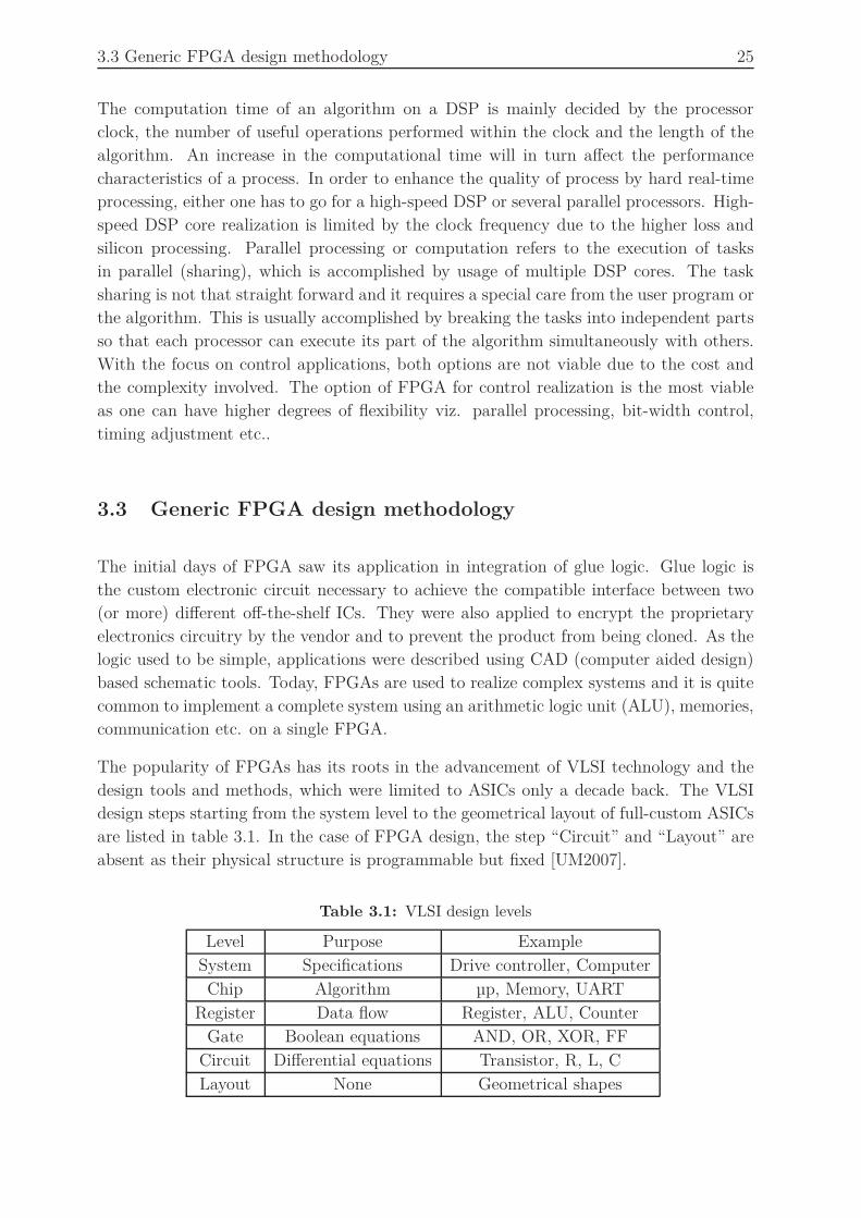
3.3 Generic FPGA design methodology 25
The computation time of an algorithm on a DSP is mainly decided by the processor
clock, the number of useful operations performed within the clock and the length of the
algorithm. An increase in the computational time will in turn affect the performance
characteristics of a process. In order to enhance the quality of process by hard real-time
processing, either one has to go for a high-speed DSP or several parallel processors. High-
speed DSP core realization is limited by the clock frequency due to the higher loss and
silicon processing. Parallel processing or computation refers to the execution of tasks
in parallel (sharing), which is accomplished by usage of multiple DSP cores. The task
sharing is not that straight forward and it requires a special care from the user program or
the algorithm. This is usually accomplished by breaking the tasks into independent parts
so that each processor can execute its part of the algorithm simultaneously with others.
With the focus on control applications, both options are not viable due to the cost and
the complexity involved. The option of FPGA for control realization is the most viable
as one can have higher degrees of flexibility viz. parallel processing, bit-width control,
timing adjustment etc..
3.3 Generic FPGA design methodology
The initial days of FPGA saw its application in integration of glue logic. Glue logic is
the custom electronic circuit necessary to achieve the compatible interface between two
(or more) different off-the-shelf ICs. They were also applied to encrypt the proprietary
electronics circuitry by the vendor and to prevent the product from being cloned. As the
logic used to be simple, applications were described using CAD (computer aided design)
based schematic tools. Today, FPGAs are used to realize complex systems and it is quite
common to implement a complete system using an arithmetic logic unit (ALU), memories,
communication etc. on a single FPGA.
The popularity of FPGAs has its roots in the advancement of VLSI technology and the
design tools and methods, which were limited to ASICs only a decade back. The VLSI
design steps starting from the system level to the geometrical layout of full-custom ASICs
are listed in table 3.1. In the case of FPGA design, the step “Circuit” and “Layout” are
absent as their physical structure is programmable but fixed [UM2007].
Table 3.1: VLSI design levels
Level Purpose Example
System Specifications Drive controller, Computer
Chip Algorithm µp, Memory, UART
Register Data flow Register, ALU, Counter
Gate Boolean equations AND, OR, XOR, FF
Circuit Differential equations Transistor, R, L, C
Layout None Geometrical shapes

26 3 Signal Processing Using FPGA
The best utilization of a device is typically achieved at gate level using register-transfer
design languages. But, the shorter time-to-market requirement combined with increasing
complexity of FPGAs are forcing a methodology shift towards the use of IP macrocells
or mega-core cells. Macrocells provide the designer with a collection of predefined func-
tions, starting from simple math operations (Add/subtract, Multiplier etc.) to complex
microprocessors and communication modules (CAN, EtherCAT etc.). Therefore the de-
signer needs to specify only the features and the attributes (e.g. accuracy). A synthesizer
will generate a hardware description code or schematic. A key point in today’s FPGA
technology is the availability of powerful design tools which
• shorten design cycle
• provide good utilization of device
• provide synthesizer options; optimization for speed or size.
These tools are based on the hardware description languages (HDLs) such as the VHDL
[AS1995] and the Verilog [PA1996]. The designer can take the advantage of HDLs to build
his own circuit by using a hierarchical and modular approach [RT1999]. The design flow
is partitioned into four steps and graphically shown in Fig. 3.1 [UM2007]. The design
entry can be graphical or text-based. A formal check that eliminates syntax errors or
Verification
Functional extraction- Database builder- Functional netlist
Design implementation- Logic synthesis- Logic partitioning- Logic fitting- Timing extraction- Programming file
Device programming
Formal check- Graphic design rules- Language syntax test
Functional simulation- Verify functionality
Timing simulation- Compare output- Check for glitch/oscillations- Check set-up hold violation
Timing analysis- Delay matrix analysis- registered performance
In-system debugging- Boundary scan- Full scan
Design entry- Graphic- Text VHDL or Verlog
Start
Figure 3.1: CAD design approach
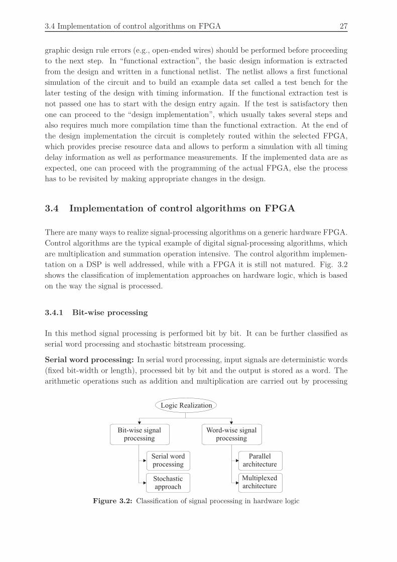
3.4 Implementation of control algorithms on FPGA 27
graphic design rule errors (e.g., open-ended wires) should be performed before proceeding
to the next step. In “functional extraction”, the basic design information is extracted
from the design and written in a functional netlist. The netlist allows a first functional
simulation of the circuit and to build an example data set called a test bench for the
later testing of the design with timing information. If the functional extraction test is
not passed one has to start with the design entry again. If the test is satisfactory then
one can proceed to the “design implementation”, which usually takes several steps and
also requires much more compilation time than the functional extraction. At the end of
the design implementation the circuit is completely routed within the selected FPGA,
which provides precise resource data and allows to perform a simulation with all timing
delay information as well as performance measurements. If the implemented data are as
expected, one can proceed with the programming of the actual FPGA, else the process
has to be revisited by making appropriate changes in the design.
3.4 Implementation of control algorithms on FPGA
There are many ways to realize signal-processing algorithms on a generic hardware FPGA.
Control algorithms are the typical example of digital signal-processing algorithms, which
are multiplication and summation operation intensive. The control algorithm implemen-
tation on a DSP is well addressed, while with a FPGA it is still not matured. Fig. 3.2
shows the classification of implementation approaches on hardware logic, which is based
on the way the signal is processed.
3.4.1 Bit-wise processing
In this method signal processing is performed bit by bit. It can be further classified as
serial word processing and stochastic bitstream processing.
Serial word processing: In serial word processing, input signals are deterministic words
(fixed bit-width or length), processed bit by bit and the output is stored as a word. The
arithmetic operations such as addition and multiplication are carried out by processing
Logic Realization
Bit-wise signalprocessing
Word-wise signalprocessing
Parallelarchitecture
Stochasticapproach
Serial wordprocessing
Multiplexedarchitecture
Figure 3.2: Classification of signal processing in hardware logic
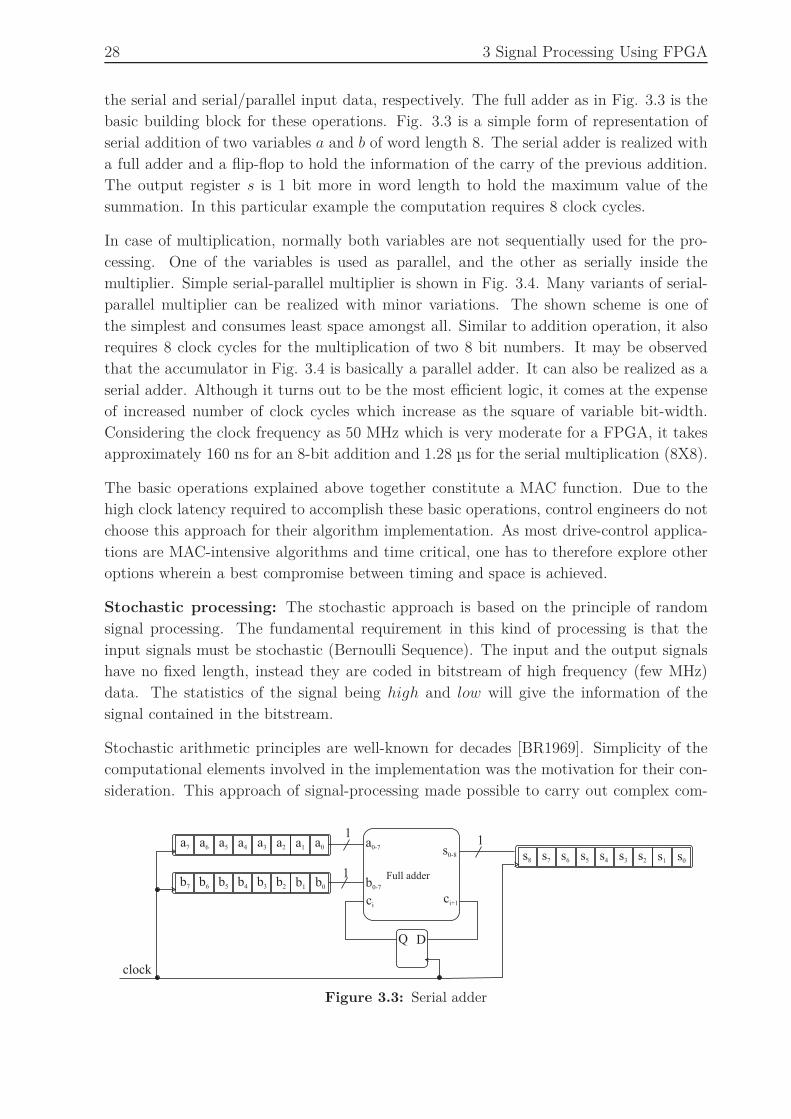
28 3 Signal Processing Using FPGA
the serial and serial/parallel input data, respectively. The full adder as in Fig. 3.3 is the
basic building block for these operations. Fig. 3.3 is a simple form of representation of
serial addition of two variables a and b of word length 8. The serial adder is realized with
a full adder and a flip-flop to hold the information of the carry of the previous addition.
The output register s is 1 bit more in word length to hold the maximum value of the
summation. In this particular example the computation requires 8 clock cycles.
In case of multiplication, normally both variables are not sequentially used for the pro-
cessing. One of the variables is used as parallel, and the other as serially inside the
multiplier. Simple serial-parallel multiplier is shown in Fig. 3.4. Many variants of serial-
parallel multiplier can be realized with minor variations. The shown scheme is one of
the simplest and consumes least space amongst all. Similar to addition operation, it also
requires 8 clock cycles for the multiplication of two 8 bit numbers. It may be observed
that the accumulator in Fig. 3.4 is basically a parallel adder. It can also be realized as a
serial adder. Although it turns out to be the most efficient logic, it comes at the expense
of increased number of clock cycles which increase as the square of variable bit-width.
Considering the clock frequency as 50 MHz which is very moderate for a FPGA, it takes
approximately 160 ns for an 8-bit addition and 1.28 µs for the serial multiplication (8X8).
The basic operations explained above together constitute a MAC function. Due to the
high clock latency required to accomplish these basic operations, control engineers do not
choose this approach for their algorithm implementation. As most drive-control applica-
tions are MAC-intensive algorithms and time critical, one has to therefore explore other
options wherein a best compromise between timing and space is achieved.
Stochastic processing: The stochastic approach is based on the principle of random
signal processing. The fundamental requirement in this kind of processing is that the
input signals must be stochastic (Bernoulli Sequence). The input and the output signals
have no fixed length, instead they are coded in bitstream of high frequency (few MHz)
data. The statistics of the signal being high and low will give the information of the
signal contained in the bitstream.
Stochastic arithmetic principles are well-known for decades [BR1969]. Simplicity of the
computational elements involved in the implementation was the motivation for their con-
sideration. This approach of signal-processing made possible to carry out complex com-
Full adder
a0a1a2a3a4a5a6a7
b1b2b3b4b5b6b7 b0
s1s2s3s4s5s6s7 s0
s8
b0-7
s0-8
ci
a0-7
Q
ci+1
D
clock
1
1
1
Figure 3.3: Serial adder
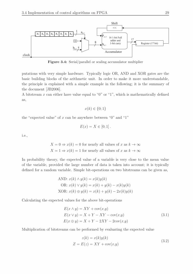
3.4 Implementation of control algorithms on FPGA 29
a0a1a2a3a4a5a6a7
b0-7
a0-7
clock
1
8
16 1-bit Fulladder and1-bit carryb0-7
P0-17
17
Register (17 bit)8
Accumulator
<<
Shift
0
Figure 3.4: Serial/parallel or scaling accumulator multiplier
putations with very simple hardware. Typically logic OR, AND and XOR gates are the
basic building blocks of the arithmetic unit. In order to make it more understandable,
the principle is explained with a simple example in the following; it is the summary of
the document [JB2006].
A bitstream x can either have value equal to “0” or “1”, which is mathematically defined
as,
x(k) ∈ 0; 1
the “expected value” of x can be anywhere between “0” and “1”
E(x) = X ∈ [0; 1] .
i.e.,
X = 0 ⇒ x(k) = 0 for nearly all values of x as k → ∞
X = 1 ⇒ x(k) = 1 for nearly all values of x as k → ∞
In probability theory, the expected value of a variable is very close to the mean value
of the variable, provided the large number of data is taken into account; it is typically
defined for a random variable. Simple bit-operations on two bitstreams can be given as,
AND: x(k) ∧ y(k) = x(k)y(k)
OR: x(k) ∨ y(k) = x(k) + y(k) − x(k)y(k)
XOR: x(k) ⊕ y(k) = x(k) + y(k) − 2x(k)y(k)
Calculating the expected values for the above bit-operations
E(x ∧ y) = XY + cov(x,y)
E(x ∨ y) = X + Y −XY − cov(x,y)
E(x⊕ y) = X + Y − 2XY − 2cov(x,y)
(3.1)
Multiplication of bitstreams can be performed by evaluating the expected value
z(k) = x(k)y(k)
Z = E(z) = XY + cov(x,y)(3.2)

30 3 Signal Processing Using FPGA
The above equation clearly indicates that the multiplication of two bitstreams can be
performed with an AND logic gate provided the “covariance” of the inputs is zero. That
implies the input signals must be “Bernoulli Sequence” (binary random signal). Assuming
that the input sequences are random signals, the procedure for other arithmetic opera-
tions can be extended. In case of addition process, it is not that straight forward as
multiplication, clearly visible from the case of OR and XOR operation in (3.1). Here we
would like to use r(k) as a help bitstream. It is also a Bernoulli Sequence, but its expected
value is known. The process is represented as follows,
z(k) = x(k) ∧ y(k) ∨ (x(k) ∨ y(k)) ∧ r(k)
= x(k)y(k) + r(k)(x(k) + y(k)) − x(k)y(k)r(k) .
With R (=E(r)) being equal to 0.5, the output of addition process Z = E(z) simplifies
to
Z = E(z) =X + Y
2. (3.3)
The scaling factor of 2 in (3.3) has to be taken care of in the actual realization. For
the further details relating to extension for other arithmetic operations refer to [BR1969]
[BC2001]. The simple arithmetic multiplication process based on the stochastic approach
is shown in Fig. 3.5. It is understood from the diagram that the multiplication of two
stochastic variables is performed by a simple two input logic AND gate. The additional
logic required to randomize the inputs a and b and derandomize the output z are the added
burden. The randomizer converts the deterministic input signals a and b into stochastic
bitstreams x and y and the derandomizer converts back the output z to a deterministic
signal Z with a finite delay.
The quality of processing is heavily dependent on the randomization. The reason is clear
from (3.1): The input bitstreams should behave as a random sequence and have the
minimum correlation or covariance between them. To realize a practical random-signal
source one has to depend on pseudo-random generators, which can only generate finite
sequences. Coming to the derandomizer which is supposed to remove the random noise
from the output bitstream, the process quality depends on the number of sequences of
bitstream taken for conversion. The higher the number of sequence, the better is the
result. That implies added delay in the output filtering. This delay can be reduced either
Randomizer
>b n
nRandom signalgenerator-2
>a n
nRandom signalgenerator-1
Randomizer
1
1
bit-stream
bit-stream
1
bit-streamderandomizer
n
x
y
z Z
f
f
Figure 3.5: Multiplication process in stochastic approach
3.4 Implementation of control algorithms on FPGA 31
by increasing the bitstream rate (by increasing f) or by reducing the number of samples
for derandomization at the cost of increased random noise in the output.
Few decades back, stochastic signal processing might have had a relevance of applica-
tion because people were ready to compromise process quality for hardware logic. But
in today’s scenario the technology is capable of fabricating chips with millions of com-
putational elements at extremely low cost and space. Hence stochastic signal processing
seems to have no future in MAC-intensive applications. Comparison of bit-wise signal
processing methods is summarized in Table 3.2.
Table 3.2: Comparison of bit-wise signal-processing methods
Serial-word Stochastic
Hardware Smaller Negligible
(arithmetic operation)
Additional hardware Generating control Randomization and
sequences derandomization
Error in processing Exists No
Communication More wires and complex Single wire and simple
Clock frequency Moderate frequency Needs comparatively
yields better results very high frequency
Verdict Still suitable In today’s scenario
not suitable
3.4.2 Word-wise processing
The study of bit-wise processing in the previous section 3.4.1 revealed that both methods
are efficient for space utilization. However, in the present scenario this approach has
not made any impact on attracting designers. By today’s cheap and densely available
logic, designers are pushed to focus more on timing and accuracy of processing instead
of logic space. It is also more relevant to FPGAs, because the present-day FPGA not
only consists of programmable logic blocks but also of a variety of hardwired embedded
units like multipliers, MAC units etc. which can be used directly to perform arithmetic
operations.
The word-wise processing can be classified into two categories based on the FPGA resource
sharing viz. fully-parallel and multiplexed. In these both approaches signal processing is
performed word by word in parallel. In the case of fully parallel architecture, hardware
resources are fixed to every mathematical operation, while in multiplexed architecture
the resources are shared by different operations. In order to understand the difference

32 3 Signal Processing Using FPGA
between these two approaches, let us consider the example of coordinate transformation
which is presented in (3.4).
usα = usd·sin(ǫ) − usq·cos(ǫ)
usβ = usd·cos(ǫ) + usq·sin(ǫ)(3.4)
Let us not bother what these variables stand for in (3.4), take it instead as a simple
arithmetic equation. This involves four multiplications and two summations, which is
graphically represented in Fig. 3.6(a). The same functionality can also be realized as
shown in Fig. 3.6(b) where the resource (multiplier) is shared in-time for performing
the multiplication. Designing such algorithms requires additional intelligent routing and
storing of input and output data. This can be accomplished by a simple logic function
using multiplexer, register and delay circuits. In the approach the resource is shared by
multiplexing the inputs hence it is termed as “multiplexed architecture” and the other as
“fully-parallel architecture”. It is obvious that the multiplexed architecture takes more
clock cycles compared to its counterpart to accomplish an operation.
usqusd cos(ǫ) sin(ǫ)
usα usβ
(a) Fully-parallel (Multipliers=4)
Reg Reg
delay
usqusd cos(ǫ)sin(ǫ)
usα usβ
(b) Multiplexed (Multipliers=2)
Figure 3.6: Fully-parallel and multiplexed architecture-based realization for coordinate trans-
formation
The implementation shown in Fig. 3.6(b) is a simple example to give an idea how the
resources can be shared. The shown functionality can also be realized using the shared
adders along with the multipliers. The main motive behind sharing the resources is to
achieve the optimized utilization of FPGA space when the algorithm is not possible to
be implemented using fully-parallel architecture. For example the functionality in (3.4)
can also be realized using a single multiplier when resources are critical on FPGA. It is
obvious that as the resource shared by operations increases, the associated logic also starts
becoming complex. It is finally left to the individual designer depending on the space,
the resource availability and the timing requirements to choose the depth of multiplexing
he has to employ for sharing.
In order to have more realistic insight of multiplexed architecture for realizing electrical
drive control, in the following subsection an example of current controller is discussed.
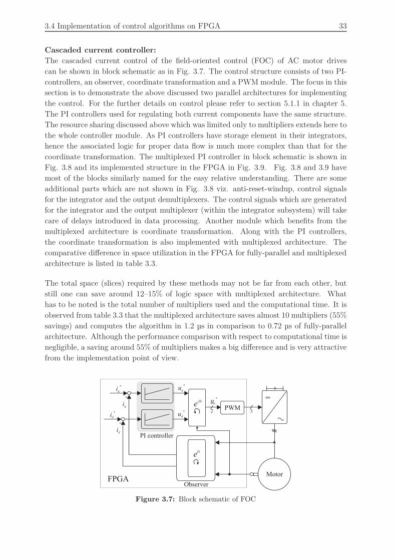
3.4 Implementation of control algorithms on FPGA 33
Cascaded current controller:
The cascaded current control of the field-oriented control (FOC) of AC motor drives
can be shown in block schematic as in Fig. 3.7. The control structure consists of two PI-
controllers, an observer, coordinate transformation and a PWM module. The focus in this
section is to demonstrate the above discussed two parallel architectures for implementing
the control. For the further details on control please refer to section 5.1.1 in chapter 5.
The PI controllers used for regulating both current components have the same structure.
The resource sharing discussed above which was limited only to multipliers extends here to
the whole controller module. As PI controllers have storage element in their integrators,
hence the associated logic for proper data flow is much more complex than that for the
coordinate transformation. The multiplexed PI controller in block schematic is shown in
Fig. 3.8 and its implemented structure in the FPGA in Fig. 3.9. Fig. 3.8 and 3.9 have
most of the blocks similarly named for the easy relative understanding. There are some
additional parts which are not shown in Fig. 3.8 viz. anti-reset-windup, control signals
for the integrator and the output demultiplexers. The control signals which are generated
for the integrator and the output multiplexer (within the integrator subsystem) will take
care of delays introduced in data processing. Another module which benefits from the
multiplexed architecture is coordinate transformation. Along with the PI controllers,
the coordinate transformation is also implemented with multiplexed architecture. The
comparative difference in space utilization in the FPGA for fully-parallel and multiplexed
architecture is listed in table 3.3.
The total space (slices) required by these methods may not be far from each other, but
still one can save around 12–15% of logic space with multiplexed architecture. What
has to be noted is the total number of multipliers used and the computational time. It is
observed from table 3.3 that the multiplexed architecture saves almost 10 multipliers (55%
savings) and computes the algorithm in 1.2 µs in comparison to 0.72 µs of fully-parallel
architecture. Although the performance comparison with respect to computational time is
negligible, a saving around 55% of multipliers makes a big difference and is very attractive
from the implementation point of view.
PWM
Motor
Observer
ud
*
-iq
id
*
-id
e-je
iq
*
us
*
uq
*
2
eje
PI controller
3
FPGA
Figure 3.7: Block schematic of FOC
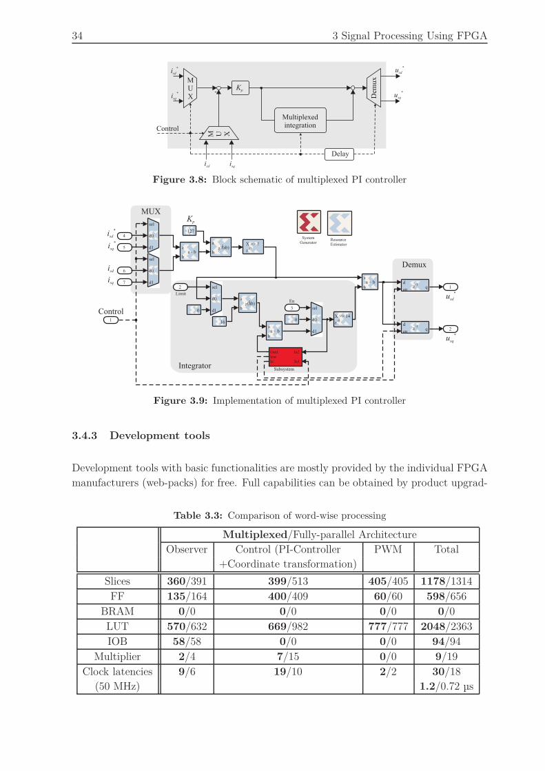
34 3 Signal Processing Using FPGA
-
usd
*
usq
*
isd isq
Multiplexedintegration
Kp
isd
*
isq
*
MUX D
emux
M U X
Delay
Control
Figure 3.8: Block schematic of multiplexed PI controller
Kp
2
usq
*
1
usd
*
In2
Sel
Out1lowhi
Subsystem
X >> 14
z-0
X >> 7
z-0
ResourceEstimator
d
enqz
-1
d
enqz
-1
sel
d0
d1sel
d0
d1
sel
d0
d1
sel
d0
d1
a
b(ab)z
-3
a
b(ab)z-3
16
127
0
0
a
ba + b
a
ba + b
a
ba - b
SystemGenerator
7isq
6isd
5
4
3
En
2
Limit
1
Control
Integrator
Demux
MUX
isq
*
isd
*
Figure 3.9: Implementation of multiplexed PI controller
3.4.3 Development tools
Development tools with basic functionalities are mostly provided by the individual FPGA
manufacturers (web-packs) for free. Full capabilities can be obtained by product upgrad-
Table 3.3: Comparison of word-wise processing
Multiplexed/Fully-parallel Architecture
Observer Control (PI-Controller PWM Total
+Coordinate transformation)
Slices 360/391 399/513 405/405 1178/1314
FF 135/164 400/409 60/60 598/656
BRAM 0/0 0/0 0/0 0/0
LUT 570/632 669/982 777/777 2048/2363
IOB 58/58 0/0 0/0 94/94
Multiplier 2/4 7/15 0/0 9/19
Clock latencies 9/6 19/10 2/2 30/18
(50 MHz) 1.2/0.72 µs

3.5 Summary 35
ing which come with a premium, e.g. Xilinx provides the ISE foundation and Altera the
Quarteress-II. These big players also support development tools which can be used along
with the Matlab/Simulink platform. They are called “System Generator” from Xilinx
and “DSP Builder” from Altera. These tools are very user-friendly and have enough re-
sources to realize most of applications; they are extremely useful for prototyping. For the
optimized realization it is always preferred to code either in VHDL or Verilog. There are
other individual vendors who provide development environment for these FPGAs such as
Aldec, Mentor-Grafics, Simplicity-Synopsys. It comes at a real premium for more user
friendly and better features.
The Matlab/Simulink-based tools are very user-friendly for most drives engineers as they
are like a standard tool used for analytical and simulation studies of dynamic systems. The
FPGA tools running on Matlab give also greater flexibility in detailed simulation studies.
These tools have limited capabilities but are good enough for most of the development
applications. Some special cases may require small modifications in the final bit-files in
their own foundation applications (e.g. ISE and Quarteress).
It is a fact that the Simulink-based tools are simpler to use for the development. The
procedure of generating mapping bit-file for a FPGA involves some intermediate steps.
First the “.m” code from Simulink is compiled to “C-program” code, and then it is con-
verted to behavioral HDL and later in design implementation the final mapping bit-files
are generated. As too many compilations are involved before a HDL code is ready, it
is very difficult to ensure that the final logic design will have optimal space usage. It
is understood that if the development is done completely using the behavioral HDL, it
is possible to ensure better hardware usage. This contradicts to cheaply available logic.
However, depending on the requirements one should make proper compromise on this
aspect.
3.5 Summary
In this chapter, the design methodology for FPGAs, the different approaches of logic
implementations and the details of development tools available from the manufacturers
are discussed. It was found in the course of study that a serial approach for the logic
implementation is not suitable in the present-day scenario. Word-wise approach for the
processing is more relevant, especially with FPGAs. To address the optimal usage of finite
resources on a FPGA a multiplexed architecture is presented. The greater advantage of
this method is demonstrated with a current controller example.


37
4 Analog-to-Digital Conversion Using Delta-Sigma
(∆Σ) Modulator
The control platform of an electrical drive shown in Fig. 1.1 consists of two fundamental
parts, the controller and the data acquisition. The controller regulates command values
which can be current, torque, flux, speed or voltage and the data acquisition system ac-
quires signals to incorporate the closed-loop control. In drive-control applications, motor
currents, rotor position and DC-bus voltage are essential to generate feedback signals.
As the motor current and the inverter DC-bus voltage are analog signals they require an
analog-to-digital converter (ADC) to process them in digital domain. Position sensors
differ in sensing technology and output data representation. Importantly there are four
variants of sensors among which three are encoders namely absolute, incremental and
sine-cosine, and the other being resolver. The output signal from sine-cosine encoder and
resolver are analog while absolute and incremental encoders outputs are in digital or bi-
nary form. Hence depending on the position sensor used, a suitable ADC for processing
is required . The efficient conversion of these analog signals into digital domain plays a
vital role in deciding the overall system performance. This motivates to have a detailed
understanding of the data converters.
The data acquisition is a key component to determine the control performance. The
control dynamic is dictated by the measurement delay and the steady-state regulation
is decided by the resolution of the acquired signal. In this chapter the focus is on the
utilization of a ∆Σ modulator-based ADC instead of a conventional multi-bit ADC for data
acquisition. The ∆Σ ADC in principle consists of two parts, modulator and filter. The
filter is preferred to be an independent unit to shape the performance of the ADC. Unlike
with the conventional multi-bit ADC, with a ∆Σ ADC the bandwidth and resolution of the
converted signal can be adjusted in a considerable range. This is an additional flexibility
which can be exploited by the design engineer to meet the specifications. Even though
∆Σ ADCs are quite popular in speech processing, from the application perspective they
are always considered as best in class for resolution and poor in bandwidth. However, one
can investigate how they can be made fit to meet the drive-control requirements. Hence
in this chapter the motor current measurement is taken for case study.
As the data rate of these modulators is in the range of tens of MHz, the associated filters
are supposed to work at the same rate. From practical reasons, a dedicated hardware
is more suitable to realize them. However, in the present-day scenario the FPGA (field
programmable gate array) is more appropriate and hence the same is considered for imple-
mentation. These modulators virtually need only a single line of connection to transmit
the bitstream to the FPGA. The bitstream has binary states which implies simple isolation

38 4 Analog-to-Digital Conversion Using Delta-Sigma (∆Σ) Modulator
and error-free data transmission (if optical transmission is employed) . These inherent
advantages make them more attractive for practical reasons.
The chapter 4 is subdivided as follows: In section 4.1, the principles of different ADC
architectures and the fundamentals of oversampled ∆Σ modulators are discussed. This
is followed by a detailed investigation on different filter topologies for ∆Σ modulators
in section 4.2. The section also describes the selection criterion which is based on the
feasibility of FPGA and setting the filter specifications according to the drive-control
requirements. In section 4.3 implementation details of the selected filters are discussed
with detailed characterization of space on FPGA. Experimental validation performed by
evaluating resolution and bandwidth from the signal spectrum of the implemented output
filters and comparison with ideal performance are described in section 4.4. Finally the
derived conclusions are given in section 4.5.
4.1 Principle of analog-to-digital conversion
Real-world signals are analog in nature; continuous in amplitude and time. To utilize
their equivalent values for efficient digital signal processing it is necessary to convert
them to digital form using analog-to-digital converters (ADCs). After the conversion,
the signal becomes discrete in amplitude and time. Hence the signal’s resolution and
bandwidth become finite. Many variants of ADCs are commercially available in the
market, they are based on one of the two important conversion principles namely Nyquist
Rate and Oversampling. Different variants of ADCs are shown on the graph with respect
to their characteristics of bandwidth and resolution in Fig. 4.1. Among them successive
approximation register (SAR) and pipelined ADCs are well-known Nyquist-rate ADCs
and the ∆Σ is the only popular oversampling ADC.
Data acquisition specific to current measurement plays a very important and critical role
in electrical drive-control applications and influences directly the control performance. In
Res
olu
tio
n (
bit
s)
Sampling rate (Hz)
8
10
12
14
16
18
20
22
24
10 100 1k 10k 100k 1M 10M 100M 1G1
DSDS
SAR
PipelineIndustry
measurement
Voice-bandaudio
Dataacquisation
High speedinstrumentation,
video, etc.
Figure 4.1: Resolution vs. speed of different ADCs

4.1 Principle of analog-to-digital conversion 39
order to improve controller performance, it is necessary that the current measurement
unit should be adequate in terms of accuracy or resolution and have good dynamics
or minimum delay. Error in magnitude (due to quantization or resolution) which is a
measure of accuracy increases the control error and higher delay restricts the achievable
closed-loop bandwidth of the controller. The SAR-type ADCs are the most commonly
used in drives industry because of their availability in many variants with reasonable
performance. With advancements in the field of analog and digital microelectronics ∆Σ-
ADCs are becoming more and more popular. Traditionally they are also known as 1-bit
high-resolution low-speed ADCs. A ∆Σ-ADC consists of two parts, the ∆Σ modulator and
a low-pass filter which removes high quantization noise from 1-bit data. Commercially,
separate modulators as well as complete ADC including the filter are available.
The low-pass filter is connected directly to the modulator’s output which indicates it has to
work at high sample rates. It can be realized by an application-specific integrated circuit
(ASIC) or a FPGA which support a dedicated hardware. DSPs are not suitable due to
their sequential execution and low sampling-rate capabilities. Among the hardware logic,
FPGAs are the best choice in the present-day scenario. In this chapter a commercially
available ∆Σ modulator is used in conjunction with a low-pass filter designed on the FPGA
platform. The second-order 1-bit ∆Σ modulator is the most common and cheapest in the
market. It is therefore chosen for the investigation.
4.1.1 Basics of ADC
The process of analog-to-digital conversion consists of two distinct steps:
1. converting time-continuous signal to a time-discrete signal by sample and hold
2. converting continuous amplitude to discrete amplitude by quantization.
The process is represented in Fig. 4.2, where x(n) is the sampled signal of a continu-
ous input x(t) at the rate of fs = 1Ts
and y(n) is the quantized output of x(n). For an
ADC error due to the quantization process is inevitable [AS1996]. To analyze the pro-
cess of conversion usually following assumptions are made regarding quantization noise
[WB1948]:
• The error sequence eq(n) is statistically independent from the input sequence x(n):
This means that the quantizer can be modeled by adding a sampled stationary
random sequence uncorrelated to the sampled input sequence .
• The probability density of the random error sequence has uniform distribution over
the range of ± ∆2
(half of the quantization step).
• The error sequence eq(n) is independent of the sampling frequency and uniformly
distributed, usually taken as flat power spectral density, a characteristic of the
white-noise process.
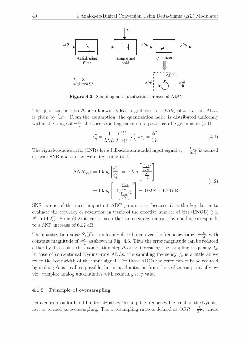
40 4 Analog-to-Digital Conversion Using Delta-Sigma (∆Σ) Modulator
Antialiasingfilter
Sample andhold
Quantizer
x(t) x(n) y(n)
Ts
x(n) y(n)
e (n)q
Ts =1/f
x(n)=x(nT )s
s
Figure 4.2: Sampling and quantization process of ADC
The quantization step ∆, also known as least significant bit (LSB) of a ”N” bit ADC,
is given byVref2N
. From the assumption, the quantization noise is distributed uniformly
within the range of ±∆2, the corresponding mean noise power can be given as in (4.1).
e2q =
1
LSB
∫ LSB2
−LSB2
[
e2q
]
deq =∆2
12(4.1)
The signal-to-noise ratio (SNR) for a full-scale sinusoidal input signal ex =Vref2√
2is defined
as peak SNR and can be evaluated using (4.2).
SNRpeak = 10log
[
e2x
e2q
]
= 10log
Vref2√
2
2
∆2
12
= 10log
12
[Vref2√
2
]
[Vref2N
]2
2
= 6.02N + 1.76 dB
(4.2)
SNR is one of the most important ADC parameters, because it is the key factor to
evaluate the accuracy or resolution in terms of the effective number of bits (ENOB) (i.e.
N in (4.2)). From (4.2) it can be seen that an accuracy increase by one bit corresponds
to a SNR increase of 6.02 dB.
The quantization noise Se(f) is uniformly distributed over the frequency range ±fs2
, with
constant magnitude of ∆2
12fsas shown in Fig. 4.3. Thus the error magnitude can be reduced
either by decreasing the quantization step ∆ or by increasing the sampling frequency fs.
In case of conventional Nyquist-rate ADCs, the sampling frequency fs is a little above
twice the bandwidth of the input signal. For these ADCs the error can only be reduced
by making ∆ as small as possible, but it has limitation from the realization point of view
viz. complex analog uncertainties with reducing step value.
4.1.2 Principle of oversampling
Data conversion for band-limited signals with sampling frequency higher than the Nyquist
rate is termed as oversampling. The oversampling ratio is defined as OSR = fs2f0
, where
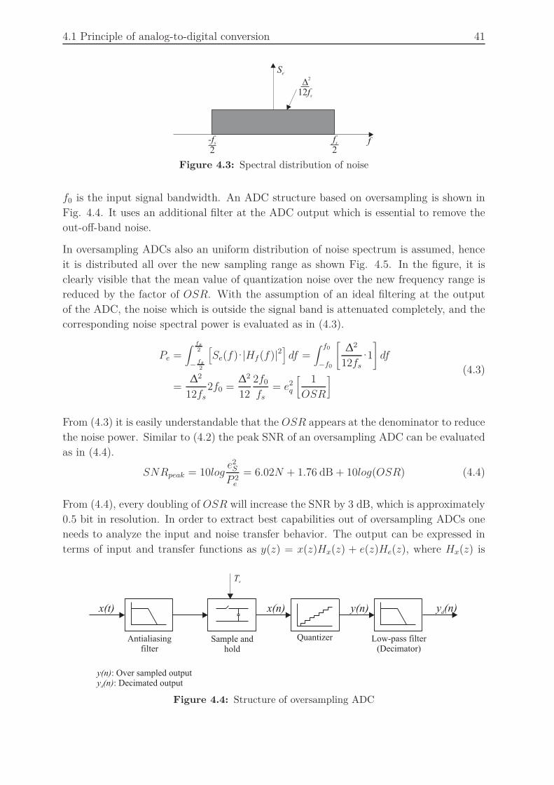
4.1 Principle of analog-to-digital conversion 41
f-fs
2fs
2
Se
D2
12fs
Figure 4.3: Spectral distribution of noise
f0 is the input signal bandwidth. An ADC structure based on oversampling is shown in
Fig. 4.4. It uses an additional filter at the ADC output which is essential to remove the
out-off-band noise.
In oversampling ADCs also an uniform distribution of noise spectrum is assumed, hence
it is distributed all over the new sampling range as shown Fig. 4.5. In the figure, it is
clearly visible that the mean value of quantization noise over the new frequency range is
reduced by the factor of OSR. With the assumption of an ideal filtering at the output
of the ADC, the noise which is outside the signal band is attenuated completely, and the
corresponding noise spectral power is evaluated as in (4.3).
Pe =∫ fs
2
−fs2
[
Se(f)·|Hf(f)|2]
df =∫ f0
−f0
[
∆2
12fs·1
]
df
=∆2
12fs2f0 =
∆2
12
2f0
fs= e2
q
[1
OSR
](4.3)
From (4.3) it is easily understandable that the OSR appears at the denominator to reduce
the noise power. Similar to (4.2) the peak SNR of an oversampling ADC can be evaluated
as in (4.4).
SNRpeak = 10loge2S
P 2e
= 6.02N + 1.76 dB + 10log(OSR) (4.4)
From (4.4), every doubling of OSR will increase the SNR by 3 dB, which is approximately
0.5 bit in resolution. In order to extract best capabilities out of oversampling ADCs one
needs to analyze the input and noise transfer behavior. The output can be expressed in
terms of input and transfer functions as y(z) = x(z)Hx(z) + e(z)He(z), where Hx(z) is
Antialiasingfilter
Sample andhold
Quantizer
x(t) x(n) y(n)
Ts
d
y(n)y (n)
: Over sampled output: Decimated output
Low-pass filter(Decimator)
y (n)d
Figure 4.4: Structure of oversampling ADC

42 4 Analog-to-Digital Conversion Using Delta-Sigma (∆Σ) Modulator
the signal transfer function and He(z) is the noise transfer function. In conventional
oversampling ADCs these transfer functions are Hx(z) = He(z) = 1. This need not be
the case always, and in fact oversampling ADCs can be designed with different Hx(z) and
He(z). This means Hx(z) leaves the input signal unchanged while He(z) reduces the in-
band noise to allow a high resolution output [CT1992] [ST2004] [NS1996] [JC1985]. E.g.
after introducing a loop filter G(z) before the quantizer and taking a negative feedback at
y(n) as shown in Fig. 4.6, the corresponding input and noise transfer functions are given
in (4.5).
Hx(z) =G(z)
1 +G(z), He(z) =
1
1 +G(z)(4.5)
Choosing G(z) such that it has very large gain within the band of interest and small gain
outside the band, then from (4.5) follows that Hx(z) ≈ 1 and He(z) ≈ 0. If G(z) is chosen
as an integrator, then Hx(z) = z-1 and He(z) = 1−z-1, which implies that the input signal
is transferred to the output with a sample delay, while the quantization noise is applied
to a first-order z domain differentiator or a high-pass filter. The corresponding output
function in z and time domain can be given as in (4.6).
y(z) = x(z)z-1 + e(z)(1 − z-1)
y(n) = x(n − 1) + e(n) − e(n − 1)(4.6)
Replacing G(z) in Fig. 4.6 by an integrator results in a first-order ∆Σ modulator and
similarly by introducing another integrator and a feedback, a second-order modulator is
realized as shown in Fig. 4.7. The DAC used in the feedback has a single-bit resolution,
is perfectly linear and is realized by a simple comparator. Consequently, if the sampling
frequency is high enough, the ∆Σ-ADC will allow to use a single-bit quantizer to achieve an
overall high resolution. By inserting more loops with integrators, it is possible to achieve
higher-order ∆Σ modulators. The signal transfer function of a nth-order modulator can be
given as Hx(z) = z-n and He(z) = (1 − z-1)n. The total quantization noise power within
-f0
Se
f0 f
aaaaaaaaaaaaaaaaaaaaaaaaaaaaaaaaaaaaaaaaaaaaaaaaaaaaaaaaaaaaaaaaaaaaaaaaaaaaaaaaaaaaaaaaaaaaaaaaaaaaaaaaaaaaaaaaaaaaaaaaaaaaaa
aaaaaaaaaaaaaaaaaaaaaaaa
Noise spectrum of Nyquist rate ADC
Noise spectrum of oversampled ADC
Noise spectrum of oversampled ADCwith ideal filtering
-fs
2
fs
2
∆2
121
2f0
∆2
121
2f0
1OSR
Figure 4.5: Noise spectrum of oversampling ADC
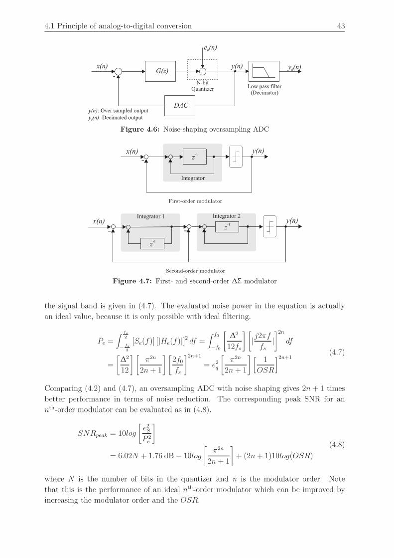
4.1 Principle of analog-to-digital conversion 43
x(n) y(n)
e (n)q
N-bitQuantizer Low pass filter
(Decimator)
y (n)dG(z)
DACy(n): Over sampled output
-
y (n)d : Decimated output
Figure 4.6: Noise-shaping oversampling ADC
x(n) y(n)z
-1
Integrator
y(n)Integrator 2
x(n)Integrator 1
-
- -
z-1
z-1
First-order modulator
Second-order modulator
Figure 4.7: First- and second-order ∆Σ modulator
the signal band is given in (4.7). The evaluated noise power in the equation is actually
an ideal value, because it is only possible with ideal filtering.
Pe =∫ fs
2
−fs2
[Se(f)] [|He(f)|]2 df =∫ f0
−f0
[
∆2
12fs
] [
|j2πf
fs|
]2n
df
=
[
∆2
12
] [
π2n
2n+ 1
] [
2f0
fs
]2n+1
= e2q
[
π2n
2n + 1
] [1
OSR
]2n+1(4.7)
Comparing (4.2) and (4.7), an oversampling ADC with noise shaping gives 2n + 1 times
better performance in terms of noise reduction. The corresponding peak SNR for an
nth-order modulator can be evaluated as in (4.8).
SNRpeak = 10log
[
e2S
P 2e
]
= 6.02N + 1.76 dB − 10log
[
π2n
2n+ 1
]
+ (2n+ 1)10log(OSR)
(4.8)
where N is the number of bits in the quantizer and n is the modulator order. Note
that this is the performance of an ideal nth-order modulator which can be improved by
increasing the modulator order and the OSR.
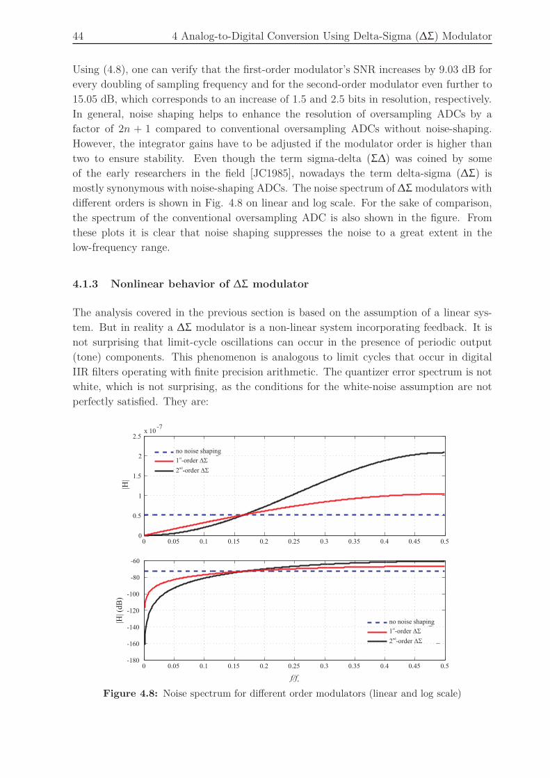
44 4 Analog-to-Digital Conversion Using Delta-Sigma (∆Σ) Modulator
Using (4.8), one can verify that the first-order modulator’s SNR increases by 9.03 dB for
every doubling of sampling frequency and for the second-order modulator even further to
15.05 dB, which corresponds to an increase of 1.5 and 2.5 bits in resolution, respectively.
In general, noise shaping helps to enhance the resolution of oversampling ADCs by a
factor of 2n + 1 compared to conventional oversampling ADCs without noise-shaping.
However, the integrator gains have to be adjusted if the modulator order is higher than
two to ensure stability. Even though the term sigma-delta (Σ∆) was coined by some
of the early researchers in the field [JC1985], nowadays the term delta-sigma (∆Σ) is
mostly synonymous with noise-shaping ADCs. The noise spectrum of ∆Σ modulators with
different orders is shown in Fig. 4.8 on linear and log scale. For the sake of comparison,
the spectrum of the conventional oversampling ADC is also shown in the figure. From
these plots it is clear that noise shaping suppresses the noise to a great extent in the
low-frequency range.
4.1.3 Nonlinear behavior of ∆Σ modulator
The analysis covered in the previous section is based on the assumption of a linear sys-
tem. But in reality a ∆Σ modulator is a non-linear system incorporating feedback. It is
not surprising that limit-cycle oscillations can occur in the presence of periodic output
(tone) components. This phenomenon is analogous to limit cycles that occur in digital
IIR filters operating with finite precision arithmetic. The quantizer error spectrum is not
white, which is not surprising, as the conditions for the white-noise assumption are not
perfectly satisfied. They are:
0 0.05 0.1 0.15 0.2 0.25 0.3 0.35 0.4 0.45 0.5-180
-160
-140
-120
-100
-80
-60
|H| (
dB
)
0 0.05 0.1 0.15 0.2 0.25 0.3 0.35 0.4 0.45 0.50
0.5
1
1.5
2
2.5x 10
-7
|H|
f/fs
no noise shaping
2 -ordernd DS
1 -orderst DS
no noise shaping
2 -ordernd DS
1 -orderst DS
Figure 4.8: Noise spectrum for different order modulators (linear and log scale)

4.1 Principle of analog-to-digital conversion 45
- the quantizer has only two output levels and
- due to oversampling successive quantizer input samples may be correlated [AS1996].
Most of the analyses [RL1994] [NP1989] which provide an exact description of the quan-
tization error spectrum and the modulator output for DC or sinusoidal inputs have been
performed for the second-order modulator using a quantizer with two or more bits. In fact,
a single-bit quantizer used in a second-order modulator can as well become overloaded,
thereby making the analysis much more difficult. The quantizer is overloaded because the
output of the second integrator can exceed by two times the modulator reference voltage
[CT1992], even for the modulator input bounded by the quantization levels ±Vref . This is
particularly true for large modulator inputs near the quantization levels. However, it has
been determined from simulations that a modified second-order architecture [BW1988]
using a single-bit quantizer can operate without integrator outputs being saturated.
According to the linearized model (4.7), e2q is a fixed value and it is expected that the
SNR will increase linearly with the signal power. However, due to presence of overload
or idle-channel tones, the SNR of a second-order modulator with a single-bit quantizer
increases linearly with input signal power only over a certain range, even though the
modulator input is well within the quantization levels. More and more overload noise
power is produced with increasing input value. Consequently, above a certain signal
power value, the SNR will start to decrease because the increase in overload noise power
is greater than the increase in signal power. This can be seen in Fig. 4.9 (taken from
[AS1996]) for input amplitudes greater than -5 dB. On the other hand, as input power
becomes smaller, the SNR decrease is caused by both decrease in signal power and the
presence of idle-channel tone noise in the signal band. To summarize: According to (4.7)
based on the linearized white-noise model, peak SNR and dynamic range should be 98 dB
for an ideal second-order ∆Σ-ADC. The realistic SNR is lower due to following aspects:
• Idle-channel tone problem resulting in a 10 dB degradation of the dynamic range.
• The quantizer overload preventing the modulator from reaching the peak SNR as
predicted by the linearized model.
-100 -90 -80 -70 -60 -50 -40 -30 -20 -10 00
20
40
60
80
Input signal amplitude (dB)
SN
R (
dB
)
Ideal (linear case)
Actual
Figure 4.9: Ideal and actual in-band SNR of second-order modulator as function of input
amplitude [AS1996]

46 4 Analog-to-Digital Conversion Using Delta-Sigma (∆Σ) Modulator
Dithering techniques, as presented in [NR1993], often break up tone structures including
overload and idle-channel tones, thereby producing a smoother power spectrum output
which has a good linear dependence between SNR and signal power and a dynamic range,
which is close to the value predicted by (4.7). Another factor which affects the in-band
SNR is the frequency of a sinusoidal input signal. The choice of a higher input frequency
will result in these harmonics falling outside the bandwidth of interest and not contribut-
ing to the in-band SNR. On the other hand, the choice of a lower input frequency will
yield poorer values of in-band SNR because the harmonics will fall inside the signal band
[AS1996].
4.2 Digital filters for noise attenuation
The delay and gain attenuation of the measured signal introduced by the current sensor
is very small and hence neglected. Additional delay and quantization error introduced
during the acquisition process have a degrading effect on the controller performance;
especially in the case of highly dynamic and precise systems. From the analysis of ∆Σ
modulators it was found that they introduce negligible delay and gain attenuation for the
input signal, but indeed add high amount of quantization noise. In order to attenuate
this, a low-pass filter is essential. It is obvious that it will impose an additional bandwidth
constraint and a phase shift to the measured input signal. To ensure there is minimum
effect on controller performance due to filtering, the design has to be considered very
carefully.
Very popular and commonly agreed as the best filter for ∆Σ modulator is the cascaded
integrator-comb (CIC) structure. However, the conventional finite impulse response (FIR)
or non-recursive filter is also employed in these kinds of applications. Usually they are
used at the second stage of filtering to shape the response for meeting the specifications. It
is seldom employed at the first stage because of high input data rate in comparison to the
signal bandwidth, which indeed requires a very high number of taps for the filter. Thus
their usage is restricted more by practical realization problems, especially the timing issue
in FPGA logic. The infinite impulse response (IIR) or recursive filters can be employed
at the first stage, but special care has to be taken for realization. The filter parameters
may need a very high bit-wide again due to a small ratio of signal to bitstream frequency.
Specific to this issue, an efficient strategy is discussed later in the implementation.
With adequate focus on implementation, CIC and IIR filters can be made more efficient
as far as logic usage is concerned. The following sections give a detailed insight on these
two filters with focus on performance analysis and feasibility study.
4.2.1 Cascaded integrator-comb filter
The CIC filter architecture based on the class of FIR filters is well suited for multi-rate
applications as proposed in [EH1981]. Primarily CIC filters are used either to reduce the
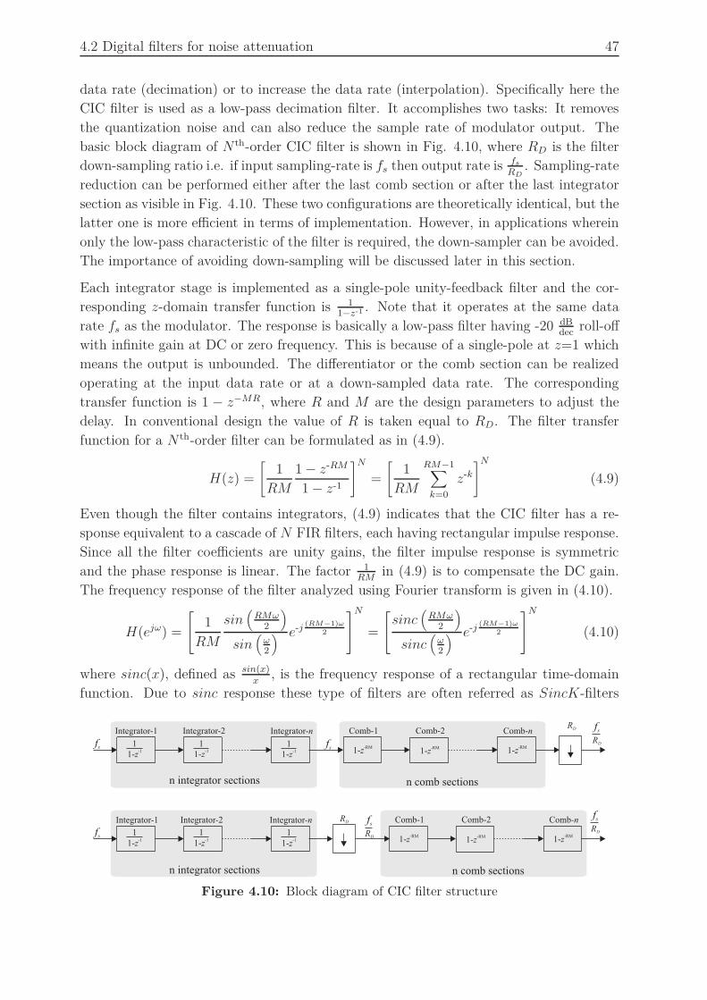
4.2 Digital filters for noise attenuation 47
data rate (decimation) or to increase the data rate (interpolation). Specifically here the
CIC filter is used as a low-pass decimation filter. It accomplishes two tasks: It removes
the quantization noise and can also reduce the sample rate of modulator output. The
basic block diagram of N th-order CIC filter is shown in Fig. 4.10, where RD is the filter
down-sampling ratio i.e. if input sampling-rate is fs then output rate is fsRD
. Sampling-rate
reduction can be performed either after the last comb section or after the last integrator
section as visible in Fig. 4.10. These two configurations are theoretically identical, but the
latter one is more efficient in terms of implementation. However, in applications wherein
only the low-pass characteristic of the filter is required, the down-sampler can be avoided.
The importance of avoiding down-sampling will be discussed later in this section.
Each integrator stage is implemented as a single-pole unity-feedback filter and the cor-
responding z-domain transfer function is 11−z-1 . Note that it operates at the same data
rate fs as the modulator. The response is basically a low-pass filter having -20 dBdec
roll-off
with infinite gain at DC or zero frequency. This is because of a single-pole at z=1 which
means the output is unbounded. The differentiator or the comb section can be realized
operating at the input data rate or at a down-sampled data rate. The corresponding
transfer function is 1 − z−MR, where R and M are the design parameters to adjust the
delay. In conventional design the value of R is taken equal to RD. The filter transfer
function for a N th-order filter can be formulated as in (4.9).
H(z) =
[
1
RM
1 − z-RM
1 − z-1
]N
=
[
1
RM
RM−1∑
k=0
z-k
]N
(4.9)
Even though the filter contains integrators, (4.9) indicates that the CIC filter has a re-
sponse equivalent to a cascade of N FIR filters, each having rectangular impulse response.
Since all the filter coefficients are unity gains, the filter impulse response is symmetric
and the phase response is linear. The factor 1RM
in (4.9) is to compensate the DC gain.
The frequency response of the filter analyzed using Fourier transform is given in (4.10).
H(ejω) =
1
RM
sin(RMω
2
)
sin(ω2
) e-j(RM−1)ω
2
N
=
sinc
(RMω
2
)
sinc(ω2
) e-j(RM−1)ω
2
N
(4.10)
where sinc(x), defined as sin(x)x
, is the frequency response of a rectangular time-domain
function. Due to sinc response these type of filters are often referred as SincK-filters
fs 1
1-z-1
Integrator-2
1
1-z-1
Integrator-n
1
1-z-1
Comb-1
1-z-RM
Comb-2 Comb-n
1-z-RM 1-z
-RM
n comb sections
n integrator sections
fs 1
1-z-1
1
1-z-1
1
1-z-1
Comb-1
1-z-RM
Comb-2 Comb-n
1-z-RM 1-z
-RM
n comb sections
RD
Integrator-1
fs
RD
RD fs
RD
fs
RD
fs
Integrator-2 Integrator-nIntegrator-1
n integrator sections
Figure 4.10: Block diagram of CIC filter structure

48 4 Analog-to-Digital Conversion Using Delta-Sigma (∆Σ) Modulator
where K stands for the filter’s order, referred as N in (4.10). Due to unity-gain feedback
integrators a register overflow is expected which is not of a serious consequence and can
easily be overcome by the following [EH1981].
• Realizing the filter with two’s complement wrap-around arithmetic.
• Choosing the range of the number system to be equal or more than the expected
maximum value.
By appropriately selecting filter design parameters N , M and R, it is possible to meet
the characteristics of a conventional FIR filter. Besides this the filter realization is very
economical in terms of logic resource as it is devoid of multipliers and a storage for
coefficients, the intermediate values being stored by the integrators themselves.
4.2.1.1 Response analysis
From the basics of digital signal processing it is clear that for a band-limited signal sampled
at a sample rate f , the input signal spectrum will start appearing at every integer multiple
of f in the frequency domain due to aliasing. The same situation occurs here as well.
As the band-limited input signal is down-sampled to fR = fsRD
, the input signal spectrum
appears at every integer multiple of fR. The spectrum after down-sampling is shown
in Fig. 4.11. The figure gives an indication that the appearance of the input spectrum
at every multiple of the down-sampling frequency will impose a constraint on the filter
bandwidth or on the selection of design parameters to avoid aliasing. To allow choosing
R independent of input bandwidth, it is necessary to avoid down-sampling. Here one can
summarize the advantages if down-sampling is avoided,
• If the input signal is not band-limited and would like to retain the bandwidth as
much as possible, as decided by the filter capabilities, in such a case down-sampling
will impose a big constraint to overcome the aliasing problems.
• By down-sampling the output, an additional dead-time is introduced which is ap-
proximately equal to 0.5 1fR
. The dead-time will keep growing as RD increases. The
additional phase introduced will add to the filter’s inherent phase.
From the above summary it is sensible to keep the output data rate at the same frequency
as the input data rate. A decade back it used to be a concern while realizing high-speed
logic, but in today’s scenario it does not make any sense. With the decision of not having
down-sampling in the filter, the factor M has no importance as the filter’s frequency
response with parameters M = 1 and R = 16 is exactly as with M = 2 and R = 8.
Henceforth with M fixed at 1, the parameter R is varied for adjusting the response. The
considered modulator is a second-order single-bit modulator with a sampling frequency of
10 MHz. From the thumb rule, the minimum order of the CIC filter should be at least one
order higher than the modulator order [NS1996]. Filter frequency responses with different

4.2 Digital filters for noise attenuation 49
0 0.02 0.04 0.06 0.08 0.1 0.12 0.14 0.16 0.18 0.2-50
-45
-40
-35
-30
-25
-20
-15
-10
-5
0
|H| (
dB
)
f/fs
Figure 4.11: Signal band appearing at integer multiple of down-sampled frequency (R=RD=16
N=1)
0 0.1 0.2-100
-80
-60
-40
-20
0
R=8
|H| (
dB
)
N=3
N=4
N=5
0 0.05 0.1-100
-80
-60
-40
-20
0
R=16
N=3
N=4
N=5
0 0.02 0.04 0.06-100
-80
-60
-40
-20
0
R=32
N=3
N=4
N=5
0 0.1 0.2
0
p
R=8
∠(r
ad)
N=3
N=4
N=5
0 0.05 0.1
0
R=16
N=3
N=4
N=5
0 0.02 0.04 0.06
0
R=32
N=3
N=4
N=5
|H| (
dB
)
|H| (
dB
)
∠(r
ad)
∠(r
ad)
f/fsf/fs f/fs
f/fsf/fs f/fs
-p
p
-p
p
-p
Figure 4.12: Frequency response of filter with different design parameters

50 4 Analog-to-Digital Conversion Using Delta-Sigma (∆Σ) Modulator
values of N and R are plotted in Fig. 4.12, where fs is modulator sampling frequency.
The observations from the figure are listed below.
• The filter has higher gain attenuation in the pass-band region.
• For a particular value of R and with an increase in the order of the filter, pass-band
attenuation and phase increase together with an increase in stop-band attenuation.
• The stop-band attenuation is mainly affected by the order of the filter N and the
bandwidth is controlled by R.
Table 4.1 shows the achievable performance with different combinations of R and N . The
minimum stop-band attenuation is almost the same for a particular order of the filter
even for different down-sampling-rates.
Table 4.1: Theoretical performance characteristics of CIC filter
R N Bandwidth Minimum stop-band attenuation
3 330 kHz -38.4 dB
8 4 290 kHz -51.7 dB
5 250 kHz -64 dB
3 165 kHz -39.4 dB
16 4 145 kHz -52.58 dB
5 125 kHz -65.7 dB
3 82.5 kHz -39.7 dB
32 4 72.5 kHz -52.93 dB
5 62.5 kHz -66.17 dB
From Fig. 4.12 it is found that the filter bandwidth is very small in almost all combina-
tions. This is because the gain starts attenuating close to zero frequency. This is one big
disadvantage of CIC filters. It is possible to enhance the bandwidth to a reasonable extent
by improving this droop characteristic in the pass-band region. Many researchers have
already proposed different methods, very popular ones are CIC compensator [DM2008]
[AN2007] [KL2006] [YC2004] [DH2009] and CIC sharpening technique [KW1997]. The
important compensation filters which were proposed and utilized in the above mentioned
publications did not focus on time-critical control applications. The following section
details the characteristics of these compensators together with the CIC filter and quali-
tatively finds whether these techniques are suitable for our application.
4.2.1.2 Inverse-Sinc function compensation
The inverse-Sinc compensation is a technique used to compensate the low-frequency droop
characteristic of CIC filters. The compensating filter gain response resembles inverse Sinc
characteristics. From the bandwidth point of view, the gain compensation is essential only
for the first lobe. However, it will work out too complex to realize such a compensation. It

4.2 Digital filters for noise attenuation 51
is more logical to design a half-band compensation, an example of a fifth-order CIC with
R=16 is shown in Fig. 4.13. Ideally it is expected from the compensation filter not to
introduce any additional phase, but in reality that is impossible; one can only try to make
it as small as possible. To achieve this transfer behavior, the compensation can either be
realized using a conventional FIR filter or just using the main Fourier components of the
inverse-Sinc function with scaled magnitudes.
The FIR-based compensator is usually realized as half-band filter and the gain perfor-
mance is proportional to the number of taps used. It is important to note that the FIR
filter can be designed as half-band filter only if the sampling-rate at the input is deci-
mated. As proposed in the previous section for not decimating the signal in the filter
makes it impossible to realize a compensation stage using this FIR topology. With the
CIC filter’s output assumed decimated, the gain and phase responses with different num-
ber of taps are shown in Fig. 4.14. As the number of taps increases in the filter, the
gain response becomes more closer to the ideal compensation, but at the same time the
phase introduced is also increasing. E.g. a filter with 16 taps is a good choice concerning
gain response while a very poor choice concerning the phase. Comparison with Fig. 4.12
indicates that the phase introduced by compensation is much higher compared to the CIC
filter. Therefore it cannot be employed in time-critical applications.
Another simple approach is to compensate only the dominant Fourier components of the
inverse-Sinc function. Ideally speaking, for exact compensation a large number of cosine
components have to be considered which results in increase of filter order and hence the
phase. The other contradicting fact is, with fewer components it is certain to have big
pass-band oscillations. A compromise is achieved by sensible use of only the main Fourier
component with the reduced gain. A similar structure has been utilized in [DM2008], and
it suggests gain calculations based on order and decimation ratio of the CIC structure. In
this particular contribution, this technique is referred as second-order-sine compensation.
It is understandable that the improved bandwidth with this technique will be lesser in
comparison to Fig. 4.13. Comparison with FIR-based compensation for gain and phase
is shown in Fig. 4.15.
With FIR-based compensation the pass-band oscillation is unavoidable with a smaller
number of taps and the phase introduced is higher compared to a fifth-order CIC filter.
0 0.05 0.1 0.15 0.2 0.25-120
-100
-80
-60
-40
-20
0
20
f/fs
|H| (
dB
) 5 -order CIC (R=16)th
ideal half-band comp.
combined response
Figure 4.13: Ideal half-band compensation

52 4 Analog-to-Digital Conversion Using Delta-Sigma (∆Σ) Modulator
0 0.05 0.1 0.15 0.2 0.25
0
10
20
30
40
|H| (
dB
)
ideal half-band comp
FIR with 8-tap
FIR with 16-tap
0 0.05 0.1 0.15 0.2 0.25
0
f/fs
∠(r
ad)
p
-p
Figure 4.14: Gain and phase response for FIR-based compensators
Although second-order sine-based compensation scores well on phase response, its band-
width is lesser in comparison to FIR-based compensation. Here are a few points to be
noted with regard to sine-based compensation in comparison to Fig. 4.15,
• provides an adequate increase in bandwidth with marginal phase increase while
ensuring a flat pass-band
• very efficient in terms of implementation and hardware utilization due to its simple
structure.
Due to these fundamental advantages, the second-order sine-based compensation is an
attractive option for compensation. In both these methods, compensation of slope in
pass-band also enhances gain in stop-band as seen from the plot of Fig. 4.15.
4.2.1.3 Sharpening technique for CIC filter
Another well-known concept to improve the pass-band gain of a CIC filter is the filter
sharpening technique. Similar to the above discussed compensation technique, the sharp-
ening technique is also used to improve transfer behavior of the filter. In [KH1977], a
method for sharpening the gain response of FIR filters using multiple times the same
filter was proposed by Kaiser and Hamming. The design method is based on an ampli-
tude change function and is strictly restricted to FIR type of filters. The filter structure
H(2−H) (where H is the transfer function of the filter to be sharpened) was first proposed
for data processing in [JT1977]. Based on this, more generalized configurations were pre-
sented later in [KW1997]. The proposed structure improved the pass-band response and
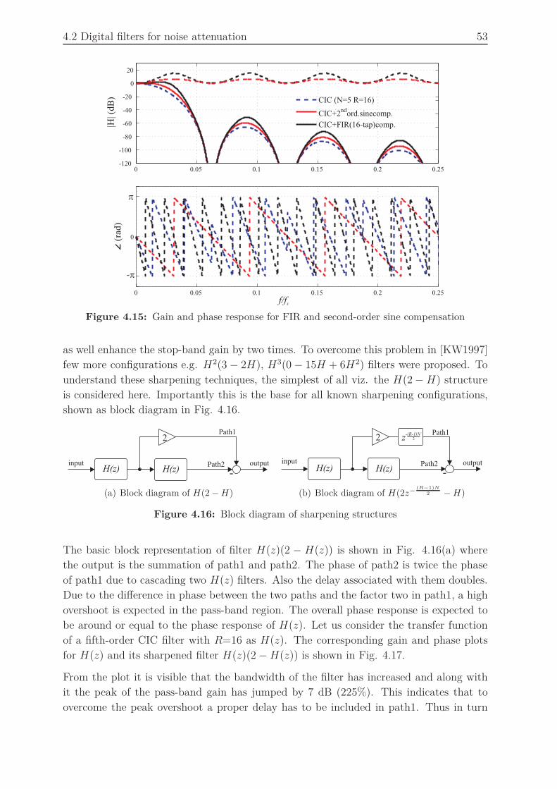
4.2 Digital filters for noise attenuation 53
0 0.05 0.1 0.15 0.2 0.25-120
-100
-80
-60
-40
-20
0
20
|H| (
dB
) CIC (N=5 R=16)
CIC+2nd
ord.sinecomp.
CIC+FIR(16-tap)comp.
0 0.05 0.1 0.15 0.2 0.25
0
∠(r
ad)
p
-p
f/fs
Figure 4.15: Gain and phase response for FIR and second-order sine compensation
as well enhance the stop-band gain by two times. To overcome this problem in [KW1997]
few more configurations e.g. H2(3 − 2H), H3(0 − 15H + 6H2) filters were proposed. To
understand these sharpening techniques, the simplest of all viz. the H(2 − H) structure
is considered here. Importantly this is the base for all known sharpening configurations,
shown as block diagram in Fig. 4.16.
Path12
Path2H(z) -H(z)
input output
(a) Block diagram of H(2 −H)
Path12
Path2H(z) -H(z)
z-(R-1)N
2
input output
(b) Block diagram of H(2z−
(R−1)N
2 −H)
Figure 4.16: Block diagram of sharpening structures
The basic block representation of filter H(z)(2 − H(z)) is shown in Fig. 4.16(a) where
the output is the summation of path1 and path2. The phase of path2 is twice the phase
of path1 due to cascading two H(z) filters. Also the delay associated with them doubles.
Due to the difference in phase between the two paths and the factor two in path1, a high
overshoot is expected in the pass-band region. The overall phase response is expected to
be around or equal to the phase response of H(z). Let us consider the transfer function
of a fifth-order CIC filter with R=16 as H(z). The corresponding gain and phase plots
for H(z) and its sharpened filter H(z)(2 −H(z)) is shown in Fig. 4.17.
From the plot it is visible that the bandwidth of the filter has increased and along with
it the peak of the pass-band gain has jumped by 7 dB (225%). This indicates that to
overcome the peak overshoot a proper delay has to be included in path1. Thus in turn
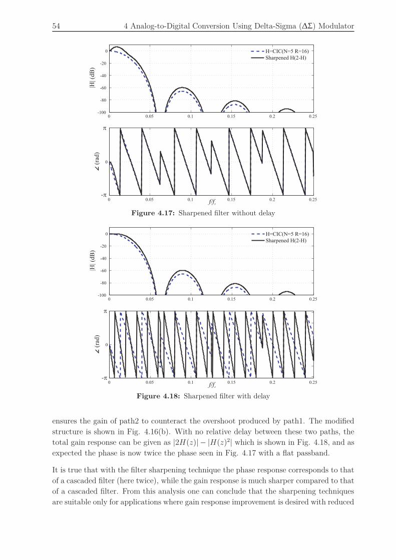
54 4 Analog-to-Digital Conversion Using Delta-Sigma (∆Σ) Modulator
0 0.05 0.1 0.15 0.2 0.25-100
-80
-60
-40
-20
0
|H| (
dB
)
H=CIC(N=5 R=16)
Sharpened H(2-H)
0 0.05 0.1 0.15 0.2 0.25
0
∠(r
ad)
p
-pf/fs
Figure 4.17: Sharpened filter without delay
0 0.05 0.1 0.15 0.2 0.25-100
-80
-60
-40
-20
0
|H| (
dB
)
H=CIC(N=5 R=16)
Sharpened H(2-H)
0 0.05 0.1 0.15 0.2 0.25
0
∠(r
ad)
p
-pf/fs
Figure 4.18: Sharpened filter with delay
ensures the gain of path2 to counteract the overshoot produced by path1. The modified
structure is shown in Fig. 4.16(b). With no relative delay between these two paths, the
total gain response can be given as |2H(z)| − |H(z)2| which is shown in Fig. 4.18, and as
expected the phase is now twice the phase seen in Fig. 4.17 with a flat passband.
It is true that with the filter sharpening technique the phase response corresponds to that
of a cascaded filter (here twice), while the gain response is much sharper compared to that
of a cascaded filter. From this analysis one can conclude that the sharpening techniques
are suitable only for applications where gain response improvement is desired with reduced

4.2 Digital filters for noise attenuation 55
transition-band and not useful for those applications with emphasis on phase response. An
important fact related to sharpening is the misleading representation of transfer function,
usually it is shown as in Fig. 4.16(a) instead of Fig. 4.16(b). The gain performance in the
pass-band and stop-band can be further improved with higher-order sharpening filters,
but one should not forget that the phase of the filter increases with every increase of order.
Due to higher phase of the overall system, it is not attractive to include sharpening along
with CIC filter structures for control applications.
With only CIC filter, it may be very difficult to meet filter specifications. Compensation
using FIR or sharpening technique may help in meeting bandwidth requirements but
introduces phase which makes them unfit. Compensation based on second-order sine
seems to be a good compromise of bandwidth and phase response and hence considered
for discussion in the next section.
4.2.2 IIR filters
The use of IIR filters for digital signal processing is well addressed in literature and text
books. The general block diagram of a simple IIR filter is shown in Fig. 4.19. Usually it is
understood as a filter with multi-bit input data and multi-bit output data. In the case of
∆Σ it is a single-bit data stream that contains the information of the input analog signal
and quantization noise. It is treated as high-frequency data with only two states. That
implies, the bitstream can directly be fed into the filter wherein the quantization noise
is extracted and only multi-bit digital data which corresponds to input analog signal
is presented at the output. The transfer function of IIR filter can be represented as
in (4.11), where a and b are the denominator and numerator polynomials, respectively.
Simple direct realization of (4.11) is shown in Fig. 4.19. The polynomial for any order
of filter configuration can be evaluated very easily using Matlab. E.g. polynomials of
the sixth-order low-pass Butterworth filter are given in Table 4.2. The polynomials given
in the table are for the case of fcfs
=0.1 (i.e. fc=100 kHz (corner frequency of filter) and
fs=10 MHz (sampling frequency of filter)).
H(z) =y(z)
x(z)=
∑ni=0 biz
−i
∑nj=0 ajz
−j(4.11)
One has to examine more carefully the numerator polynomials as they are very small. As
the filter order increases, these values are expected to reduce further. The other reason for
being small is due to the small ratio of filter corner frequency and the sampling frequency,
which is usually around this number for ∆Σ filters.
4.2.3 Filter specification
The requirement of filter characteristics employed for data conversion of motor currents
varies depending on used control scheme. Hysteresis controllers, such as in DTC (direct
torque control) demand the measurement delay to be as small as possible while in the case
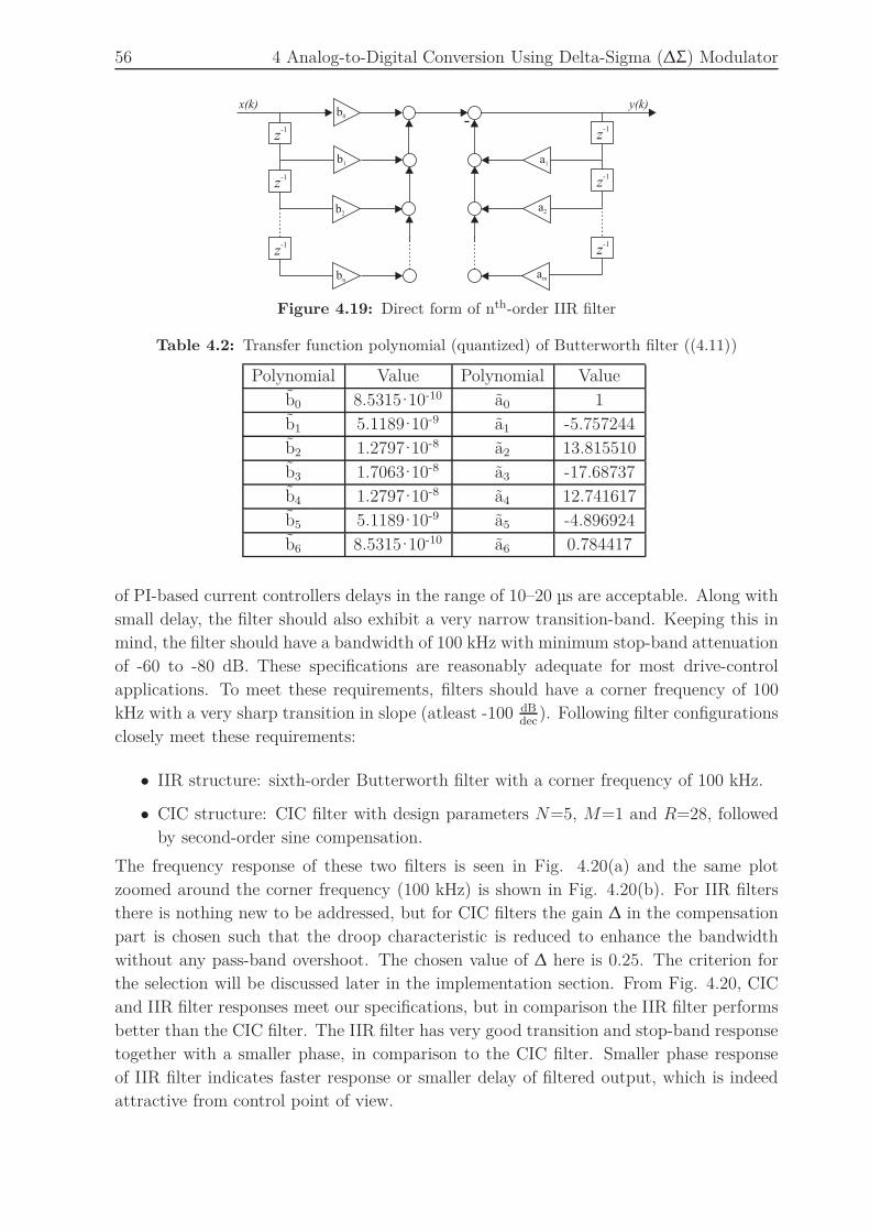
56 4 Analog-to-Digital Conversion Using Delta-Sigma (∆Σ) Modulator
b0
x(k)
-y(k)
b1
b2
bn
z-1
z-1
z-1
a1
a2
am
z-1
z-1
z-1
Figure 4.19: Direct form of nth-order IIR filter
Table 4.2: Transfer function polynomial (quantized) of Butterworth filter ((4.11))
Polynomial Value Polynomial Value
b0 8.5315·10-10 a0 1
b1 5.1189·10-9 a1 -5.757244
b2 1.2797·10-8 a2 13.815510
b3 1.7063·10-8 a3 -17.68737
b4 1.2797·10-8 a4 12.741617
b5 5.1189·10-9 a5 -4.896924
b6 8.5315·10-10 a6 0.784417
of PI-based current controllers delays in the range of 10–20 µs are acceptable. Along with
small delay, the filter should also exhibit a very narrow transition-band. Keeping this in
mind, the filter should have a bandwidth of 100 kHz with minimum stop-band attenuation
of -60 to -80 dB. These specifications are reasonably adequate for most drive-control
applications. To meet these requirements, filters should have a corner frequency of 100
kHz with a very sharp transition in slope (atleast -100 dBdec
). Following filter configurations
closely meet these requirements:
• IIR structure: sixth-order Butterworth filter with a corner frequency of 100 kHz.
• CIC structure: CIC filter with design parameters N=5, M=1 and R=28, followed
by second-order sine compensation.
The frequency response of these two filters is seen in Fig. 4.20(a) and the same plot
zoomed around the corner frequency (100 kHz) is shown in Fig. 4.20(b). For IIR filters
there is nothing new to be addressed, but for CIC filters the gain ∆ in the compensation
part is chosen such that the droop characteristic is reduced to enhance the bandwidth
without any pass-band overshoot. The chosen value of ∆ here is 0.25. The criterion for
the selection will be discussed later in the implementation section. From Fig. 4.20, CIC
and IIR filter responses meet our specifications, but in comparison the IIR filter performs
better than the CIC filter. The IIR filter has very good transition and stop-band response
together with a smaller phase, in comparison to the CIC filter. Smaller phase response
of IIR filter indicates faster response or smaller delay of filtered output, which is indeed
attractive from control point of view.

4.3 Implementation 57
0 0.02 0.04 0.06 0.08 0.1 0.12-150
-100
-50
0
|H| (
dB
)
CIC (N=5,R=28)
sin compensation2
0 0.02 0.04 0.06 0.08 0.1 0.12
0
∠(r
ad)
f/f s
p
-p
(CIC+sin ) compensation2
IIR 6 -orderth
(a) Gain and phase plot of CIC and IIR filters
0 0.002 0.004 0.006 0.008 0.01 0.012 0.014 0.016 0.018 0.02-10
-5
0
5
10
|H| (
dB
)
0 0.002 0.004 0.006 0.008 0.01 0.012 0.014 0.016 0.018 0.02
0
∠(r
ad)
f/f s
p
-p
CIC (N=5,R=28)
sin compensation2
(CIC+sin ) compensation2
IIR 6 -orderth
(b) Zoom around the corner frequency of the designed filters
Figure 4.20: Theoretical performance comparison of IIR and CIC filters
4.3 Implementation
Details of the test bench are listed in Appendix A.1. The above selected filter structures
were implemented on a Xilinx Virtex-2P-XC2VP30 FPGA. The logic development of these
algorithms is carried out with the Xilinx System-Generator toolbox.
4.3.1 CIC with second-order sine compensation
The cascade of CIC filters with the compensation structure is represented in block
schematic in Fig. 4.21. The used parameters of the CIC filter are the same as above
(N=5, R=28 and M=1). The transfer function of the CIC filter has been evaluated from
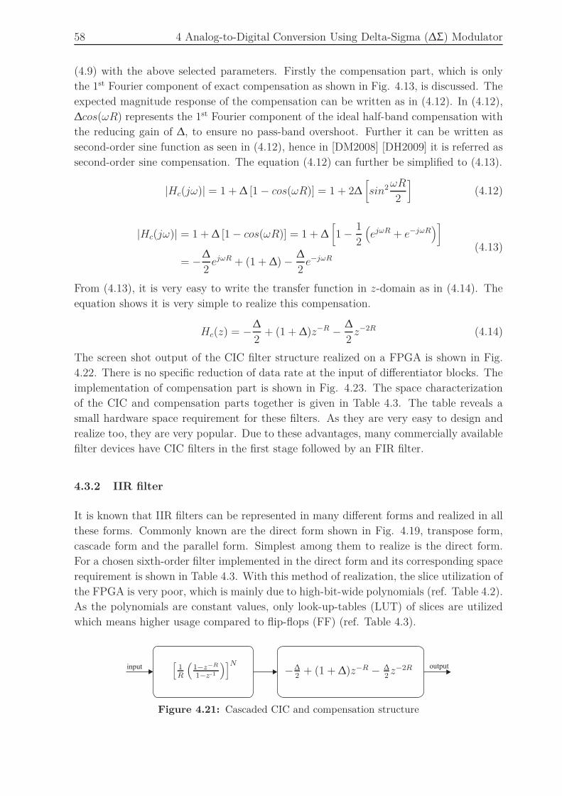
58 4 Analog-to-Digital Conversion Using Delta-Sigma (∆Σ) Modulator
(4.9) with the above selected parameters. Firstly the compensation part, which is only
the 1st Fourier component of exact compensation as shown in Fig. 4.13, is discussed. The
expected magnitude response of the compensation can be written as in (4.12). In (4.12),
∆cos(ωR) represents the 1st Fourier component of the ideal half-band compensation with
the reducing gain of ∆, to ensure no pass-band overshoot. Further it can be written as
second-order sine function as seen in (4.12), hence in [DM2008] [DH2009] it is referred as
second-order sine compensation. The equation (4.12) can further be simplified to (4.13).
|Hc(jω)| = 1 + ∆ [1 − cos(ωR)] = 1 + 2∆[
sin2ωR
2
]
(4.12)
|Hc(jω)| = 1 + ∆ [1 − cos(ωR)] = 1 + ∆
[
1 −1
2
(
ejωR + e−jωR)]
= −∆
2ejωR + (1 + ∆) −
∆
2e−jωR
(4.13)
From (4.13), it is very easy to write the transfer function in z-domain as in (4.14). The
equation shows it is very simple to realize this compensation.
Hc(z) = −∆
2+ (1 + ∆)z−R −
∆
2z−2R (4.14)
The screen shot output of the CIC filter structure realized on a FPGA is shown in Fig.
4.22. There is no specific reduction of data rate at the input of differentiator blocks. The
implementation of compensation part is shown in Fig. 4.23. The space characterization
of the CIC and compensation parts together is given in Table 4.3. The table reveals a
small hardware space requirement for these filters. As they are very easy to design and
realize too, they are very popular. Due to these advantages, many commercially available
filter devices have CIC filters in the first stage followed by an FIR filter.
4.3.2 IIR filter
It is known that IIR filters can be represented in many different forms and realized in all
these forms. Commonly known are the direct form shown in Fig. 4.19, transpose form,
cascade form and the parallel form. Simplest among them to realize is the direct form.
For a chosen sixth-order filter implemented in the direct form and its corresponding space
requirement is shown in Table 4.3. With this method of realization, the slice utilization of
the FPGA is very poor, which is mainly due to high-bit-wide polynomials (ref. Table 4.2).
As the polynomials are constant values, only look-up-tables (LUT) of slices are utilized
which means higher usage compared to flip-flops (FF) (ref. Table 4.3).
input output−∆
2+ (1 + ∆)z−R − ∆
2z−2R
[1R
(1−z−R
1−z-1
)]N
Figure 4.21: Cascaded CIC and compensation structure

4.3 Implementation 59
1
y
enz-1enz-1
enz-1enz-1
enz-28enz
-28enz-28enz
-28enz-28
enz-1
a
ba + b
a
ba + b
a
ba + b
a
ba + b
a
ba + b
2
Clk
1
X
Integrator
Differentiator
Figure 4.22: Implementation of CIC filter
- /2D
1+D
1
y'en
z-28
enz-56
x (-0.125)
x 1.25
a
b
a + b
a
b
a + b
2
clk
1
y
Figure 4.23: Implementation of second-order-sine compensation
In order to overcome this drawback one can explore different forms of Butterworth filters,
e.g. a cascaded structure. In this form of realization, higher-order transfer functions are
decomposed into multiple reduced-order functions in cascade. For any even filter order,
the transfer function is decomposed into a multiple cascade of second-order filters and odd
orders as a multiple cascade of second-order filters and a first-order filter. Small sampling
time used for filter realization on the FPGA allows to approximate the process to an
analog system, as the error introduced using a simple numerical integration method such
as first-order forward Euler is negligible. Hence one can directly employ continuous-time
design rules for the filters. However, due to this discrete integration, condition for the
stability of the filter is that the poles of the transfer function must lay within the circle of
Table 4.3: Logic usage for filter realization (% of respective available resource on FPGA uti-
lized) LUT: Look-Up-Table FF: Flip-Flop
Filter type Different approaches Slices LUT FF
CIC+Compensation - 858 1252 593
(6%) (4%) (2%)
IIR-Direct 2874 5154 290
IIR approach (20%) (18%) (1%)
IIR-Cascaded 535 773 344
approach (3%) (2%) (1%)

60 4 Analog-to-Digital Conversion Using Delta-Sigma (∆Σ) Modulator
radius = 1Ts
centered at −Ts in the “s” plane. This implies, as the ratio between the filter
sampling frequency to the corner frequency is very high, the performance of analog and
discrete system will more or less be the same, as this ratio starts reducing it is necessary
to investigate the stability and the performance details more carefully.
Design method: The approach employed here can be found in textbooks on filters
[HL1979]. The transfer function of a sixth-order IIR filter and its cascaded form can be
presented as in (4.15) where it is decomposed into a cascade of three second-order filters
H(s) =ω6c
s6 + 3.863ωcs5 + 7.464ω2cs
4 + 9.141ω3cs
3 + 7.464ω4cs
2 + 3.863ω5cs+ ω6
c
=
[
ω2c
s2 + 0.517ωcs+ ω2c
] [
ω2c
s2 + 1.414ωcs+ ω2c
] [
ω2c
s2 + 1.932ωcs+ ω2c
] (4.15)
where ωc is the corner frequency of the sixth-order filter. The slowest among these three
filters has to be used in the front of the structure to avoid overflow due to high overshoot.
Implementation of individual second-order filters can be understood very simply by con-
sidering an R-L-C series circuit. The representation of the transfer function in a block
schematic is shown in Fig. 4.24. The gains used before the integrators are the ratio of
sample time Ts to time constant, which is automatically normalized. The values for these
three parameters can be chosen as given in (4.16) for the first second-order filter in (4.15)
H1(s) =
[
ω2c
s2 + 0.517ωcs+ ω2c
]
=
[1LC
s2 + RLs+ 1
LC
]
. (4.16)
For the given corner frequency ωc = 2π·100 kHz, the product of LC is fixed, thus it is
necessary to assume one among these values to fix the other. By taking C=10 µF, values
for L and R becomes 0.25 µH and 0.082 Ω, respectively. With 10 MHz of sampling fre-
quency, i.e Ts = 0.1 µs, the corresponding gains in Fig 4.24 are Tsτ1
=0.0325 and Tsτ2
=0.1214.
These values are reasonably bigger and can therefore be represented with very small bit-
wide. During implementation, only a bit-wide of 12 is utilized for these constants in all
x(t)
R L
C y(t)
ic
iout=0
1/R
t1s+1
1
Cs
x(t) y(t)
Ts
t1x(t) y(t)
-
- -
Ts
t2
Figure 4.24: Simplified block schematic of second-order low-pass filter (τ1 = LR , τ2 = RC)
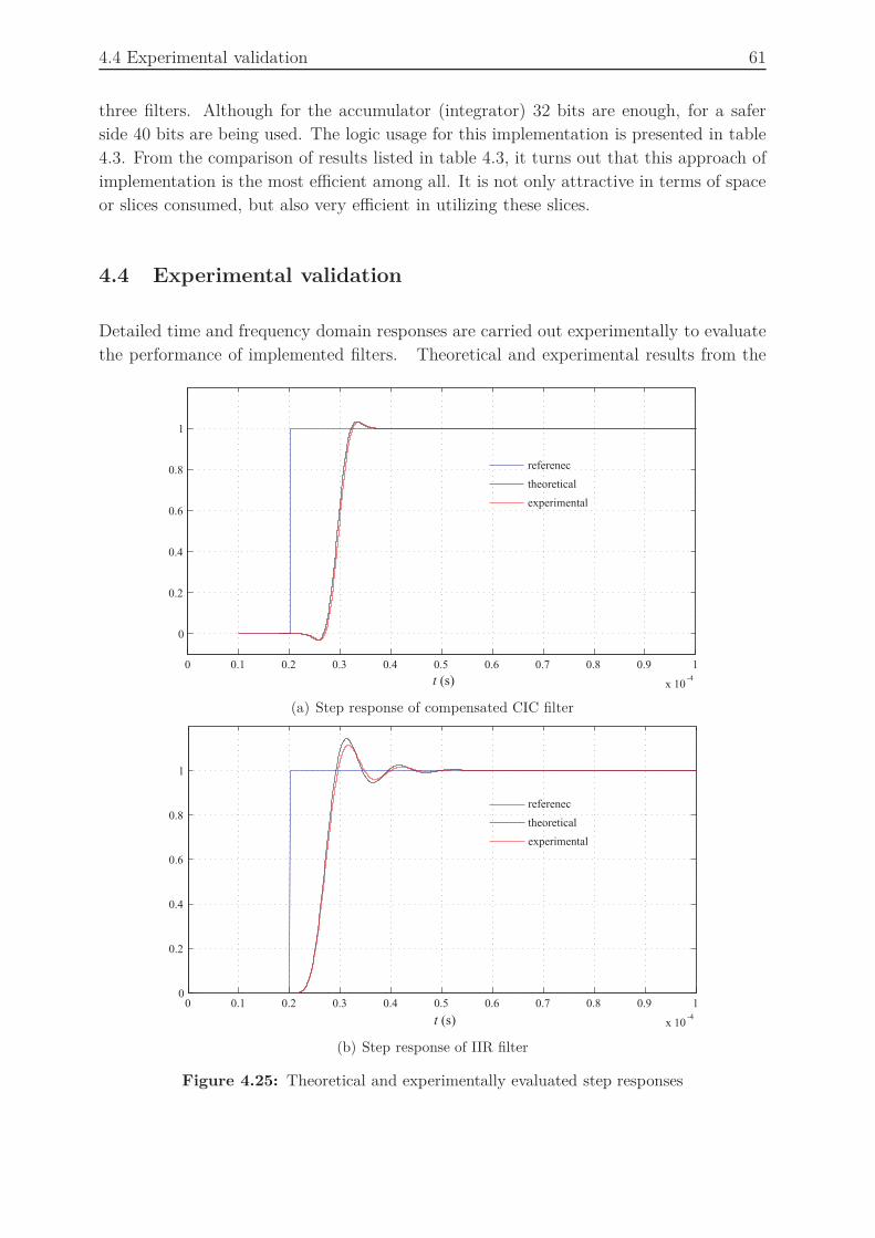
4.4 Experimental validation 61
three filters. Although for the accumulator (integrator) 32 bits are enough, for a safer
side 40 bits are being used. The logic usage for this implementation is presented in table
4.3. From the comparison of results listed in table 4.3, it turns out that this approach of
implementation is the most efficient among all. It is not only attractive in terms of space
or slices consumed, but also very efficient in utilizing these slices.
4.4 Experimental validation
Detailed time and frequency domain responses are carried out experimentally to evaluate
the performance of implemented filters. Theoretical and experimental results from the
0 0.1 0.2 0.3 0.4 0.5 0.6 0.7 0.8 0.9 1
x 10-4
0
0.2
0.4
0.6
0.8
1
referenec
theoretical
experimental
t (s)
(a) Step response of compensated CIC filter
0 0.1 0.2 0.3 0.4 0.5 0.6 0.7 0.8 0.9 1
x 10-4
0
0.2
0.4
0.6
0.8
1
referenec
theoretical
experimental
t (s)
(b) Step response of IIR filter
Figure 4.25: Theoretical and experimentally evaluated step responses

62 4 Analog-to-Digital Conversion Using Delta-Sigma (∆Σ) Modulator
0 2 4 6 8 10 12
x 104
-12
-10
-8
-6
-4
-2
0
|H| (
dB
)IIR filter
CIC filter
0 2 4 6 8 10 12
x 104
0
f (Hz)
∠(r
ad)
IIR filter
CIC filter
-2p
-p
Figure 4.26: Experimental gain and phase response for compensated CIC and IIR filters
time-domain response of both filters are shown in Fig. 4.25(a) and 4.25(b), respectively.
Experimental values match very well the theoretical values. As expected from the earlier
study, the IIR filter shows a considerable overshoot. It is important to point out that
for the CIC filter response in Fig. 4.25(a) there is no visible down-sampling rate, imply
that the output rate from the differentiators has the same data rate as the input i.e.
fs (=10 MHz). The experimental step response looks more or less continuous as each
time division (10 µs) has 100 samples. To evaluate the frequency response of the filter,
the input is driven by a varying-frequency sinusoidal signal and the corresponding filter
output signals are captured. These two are compared to evaluate gain and phase plot as
shown in Fig. 4.26. The experimental frequency response plot matches very closely the
theoretical evaluated values as shown in Fig. 4.20. To be specific the experimental values
of bandwidth for IIR and CIC filter are around 95 kHz and 105 kHz, respectively.
From the time and frequency responses one can see that the IIR filter has better per-
formance compared to the compensated CIC filter in most respects, except for a higher
overshoot in the step response.
To calculate the resolution of the ADC from its SNR, usually the in-band noise of the
signal is taken into account. This is valid provided the low-pass filter ensures the smallest
transition-band and high stop-band attenuation. The signal and the filter power spectrum
for both filter topologies are shown in Fig. 4.27(a) and 4.27(b), respectively. In these
plots the plot with blue color refers to the frequency spectrum of the modulator output
bitstream. Although it resembles the shape of an ideal modulator’s noise spectrum as in
Fig. 4.8, it has higher power. This might be due to the non idealities of the practical

4.4 Experimental validation 63
0 0.5 1 1.5 2 2.5
x 106
-150
-100
-50
0
(Hz)f
|H| (
dB
)
Spectrum of bitstream
Spectrum of compensated CIC output
(a) Power spectrum of compensated CIC filter
0 0.5 1 1.5 2 2.5
x 106
-150
-100
-50
0
(Hz)f
|H| (
dB
)
Spectrum of bitstream
Spectrum of IIR filter output
(b) Power spectrum of IIR filter
Figure 4.27: Power spectrum of ∆Σ modulator bitstream and filter output
modulator and its associated circuit on the board. From these plots the following can be
summarized for the filter spectrum:
• The designed filters have a corner frequency of 100 kHz.
• The frequency of the sinusoidal analog input signal is 75 kHz and in the output
spectrum this signal is not attenuated in both cases.
• For the CIC response in Fig. 4.27(a) the lobes are clearly visible, occurring at
multiples of fsR
.
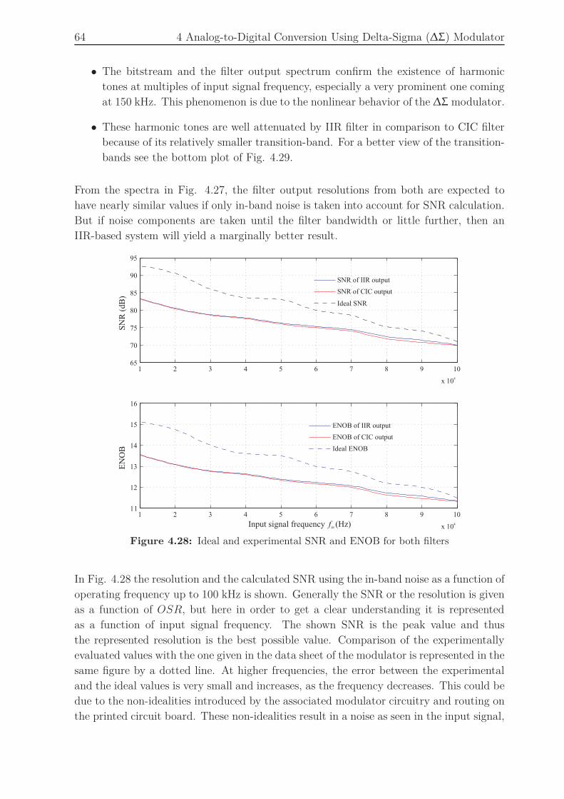
64 4 Analog-to-Digital Conversion Using Delta-Sigma (∆Σ) Modulator
• The bitstream and the filter output spectrum confirm the existence of harmonic
tones at multiples of input signal frequency, especially a very prominent one coming
at 150 kHz. This phenomenon is due to the nonlinear behavior of the ∆Σ modulator.
• These harmonic tones are well attenuated by IIR filter in comparison to CIC filter
because of its relatively smaller transition-band. For a better view of the transition-
bands see the bottom plot of Fig. 4.29.
From the spectra in Fig. 4.27, the filter output resolutions from both are expected to
have nearly similar values if only in-band noise is taken into account for SNR calculation.
But if noise components are taken until the filter bandwidth or little further, then an
IIR-based system will yield a marginally better result.
1 2 3 4 5 6 7 8 9 10
x 104
65
70
75
80
85
90
95
SN
R (
dB
)
1 2 3 4 5 6 7 8 9 10
x 104
11
12
13
14
15
16
Input signal frequency (Hz)fin
EN
OB
SNR of IIR output
SNR of CIC output
Ideal SNR
ENOB of IIR output
ENOB of CIC output
Ideal ENOB
Figure 4.28: Ideal and experimental SNR and ENOB for both filters
In Fig. 4.28 the resolution and the calculated SNR using the in-band noise as a function of
operating frequency up to 100 kHz is shown. Generally the SNR or the resolution is given
as a function of OSR, but here in order to get a clear understanding it is represented
as a function of input signal frequency. The shown SNR is the peak value and thus
the represented resolution is the best possible value. Comparison of the experimentally
evaluated values with the one given in the data sheet of the modulator is represented in the
same figure by a dotted line. At higher frequencies, the error between the experimental
and the ideal values is very small and increases, as the frequency decreases. This could be
due to the non-idealities introduced by the associated modulator circuitry and routing on
the printed circuit board. These non-idealities result in a noise as seen in the input signal,
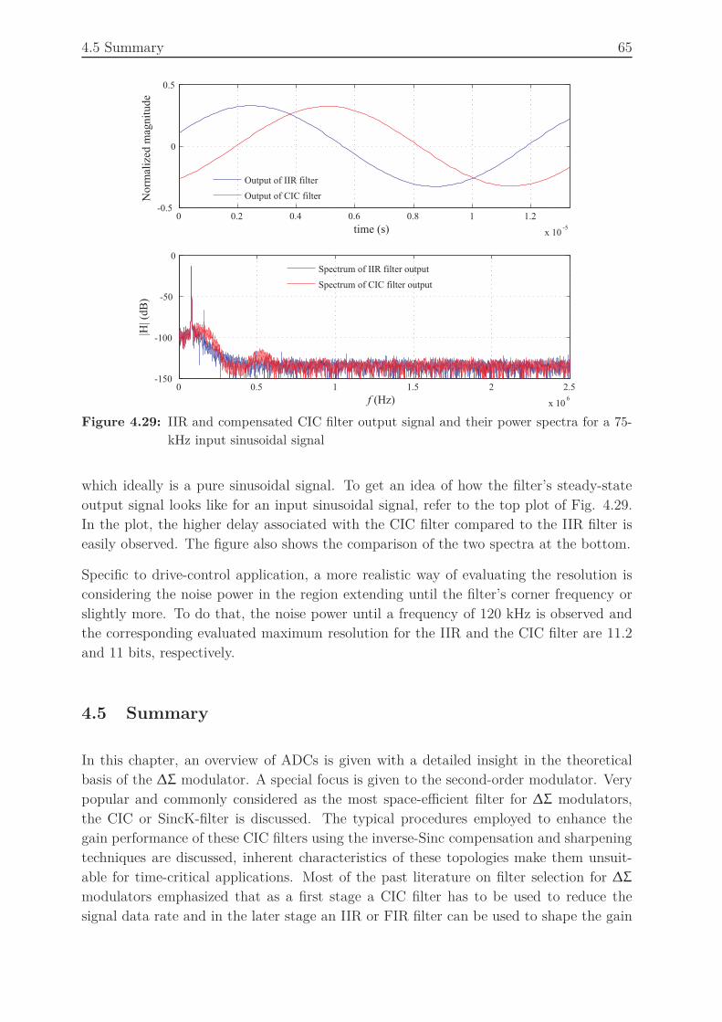
4.5 Summary 65
0 0.5 1 1.5 2 2.5
x 106
-150
-100
-50
0
f (Hz)
|H| (
dB
)
Spectrum of IIR filter output
Spectrum of CIC filter output
0 0.2 0.4 0.6 0.8 1 1.2
x 10-5
-0.5
0
0.5
Norm
aliz
ed m
agnit
ude
time (s)
Output of IIR filter
Output of CIC filter
Figure 4.29: IIR and compensated CIC filter output signal and their power spectra for a 75-
kHz input sinusoidal signal
which ideally is a pure sinusoidal signal. To get an idea of how the filter’s steady-state
output signal looks like for an input sinusoidal signal, refer to the top plot of Fig. 4.29.
In the plot, the higher delay associated with the CIC filter compared to the IIR filter is
easily observed. The figure also shows the comparison of the two spectra at the bottom.
Specific to drive-control application, a more realistic way of evaluating the resolution is
considering the noise power in the region extending until the filter’s corner frequency or
slightly more. To do that, the noise power until a frequency of 120 kHz is observed and
the corresponding evaluated maximum resolution for the IIR and the CIC filter are 11.2
and 11 bits, respectively.
4.5 Summary
In this chapter, an overview of ADCs is given with a detailed insight in the theoretical
basis of the ∆Σ modulator. A special focus is given to the second-order modulator. Very
popular and commonly considered as the most space-efficient filter for ∆Σ modulators,
the CIC or SincK-filter is discussed. The typical procedures employed to enhance the
gain performance of these CIC filters using the inverse-Sinc compensation and sharpening
techniques are discussed, inherent characteristics of these topologies make them unsuit-
able for time-critical applications. Most of the past literature on filter selection for ∆Σ
modulators emphasized that as a first stage a CIC filter has to be used to reduce the
signal data rate and in the later stage an IIR or FIR filter can be used to shape the gain
66 4 Analog-to-Digital Conversion Using Delta-Sigma (∆Σ) Modulator
response. Essentially in these investigations the phase response of the filter output was
never focused. But in time-critical applications, along with the filter’s gain response the
phase is also an essentially important factor. It is not important whether the filter has lin-
ear or non-linear phase response, compared with the magnitude of the phase angle in the
operating region of the filter. Therefore it was found and demonstrated that a multi-stage
filtering is not a good choice in this kind of applications. Also the popular sharpening
technique for CIC filters was discussed and shown that higher delays are introduced by
the cascaded structures which are also not suitable for the given requirements. From Fig.
4.14 and 4.15 it is clearly visible that even a small gain slope compensation for a CIC
filter introduces a considerable amount of delay.
Furthermore it is proposed in this chapter to use the same data rate for the integrator
and the differentiator sections of CIC filters to avoid the sampling delay which is un-
avoidable in conventional decimated configurations. The proposed concept is successfully
demonstrated and it is shown that the resulting signal is more continuous in nature.
It is also a common presumption that the single-stage IIR filters are not suitable for ∆Σ
bitstream filtering. This contribution utilized a simple design procedure for the cascaded
type IIR filter structure and it is proven that such a filter realization is more efficient in
logic usage from the FPGA point of view (see table 4.3). The consumed FPGA space
is even much smaller compared to CIC filters. Detailed analysis of the resulting noise
spectrum and the calculated SNR and ENOB shows that IIR filters outperform CIC
filters in all areas.

67
5 Design of Pulse-Width-Modulation-based Motor
Control on a FPGA
In the previous chapter the utilization of FPGAs for efficient data acquisition was dis-
cussed. In this chapter the focus is on these generic components extending their appli-
cation to realize highly dynamic PWM-based control. Well-known PWM-based control
schemes of AC drives are Field-Oriented Control (FOC) and Indirect Stator-quantity
Control (ISC). The FOC is also known as cascaded current controller and ISC as PWM-
Direct Torque Control (PWM-DTC) or Space-Vector-Modulated-DTC (SVM-DTC) or
constant-switching frequency DTC. The motivation of this chapter is to enhance the
dynamic capabilities of PWM-based controls without increasing the inverter switching
frequency, while at the same time keeping the total harmonic distortion (THD) in motor
line currents very low. The approach used to design the controller is based on the assump-
tion of a quasi-continuous realization instead of a sampled system. A quasi-continuous
system whose sample time is in the range of few hundreds of ns is a close approximation of
a continuous-time system. To achieve a high sampling rate, in today’s scenarios FPGA-
based control platforms are more relevant and are therefore considered here as well. This
chapter outlines the design procedure for the above mentioned control schemes, which is
mostly based on an analytical approach. For better readability, the chapter is divided
into two parts, FOC in the first, followed by ISC in the second.
Characteristics of highly dynamic motor drives
As the emphasis of this chapter is on highly dynamic control, it is necessary to under-
stand their characteristics and requirements very clearly. In recent times, highly dynamic
controllers are gaining more and more importance, specifically in the context of hybrid
and electric propulsion systems employed in automobiles and compact servo drives for
automation. These motors are typically characterized by a high number of pole-pairs
in the range of 5–10 [YS2009]. This circumstance implies that the electrical frequency
can go as high as 1–2 kHz and the drive should be capable of deep field-weakening or a
wide constant-power region of operation. Due to the high power density and the type of
windings used, the motor back-EMF is expected to have lower-order harmonics [EL2010]
i.e., its waveform is non-sinusoidal. The control of these motors with the state-of-the-art
regular-sampling technique would therefore result in only 5–10 samples per fundamental
cycle at high speeds (at a sampling frequency of 10 kHz). This will tend to introduce
beating effects and higher-harmonic distortion in the motor line currents. Identifying and
compensating these harmonic frequency components of the back-EMF in the control loop
is a difficult task. Hence these components always appear in the motor line currents and
introduce torque oscillations corresponding to low multiples of the fundamental frequency.
In order to overcome these problems, the closed-loop bandwidth for the torque control
has to be increased adequately.
68 5 Design of Pulse-Width-Modulation-based Motor Control on a FPGA
With the present regular-sampling control technique, the achievable controller bandwidth
is restricted due to high dead-time in the loop. The controller sampling frequency is in
the range of 10–20 kHz. Even with such high sampling rates, the achievable closed-loop
bandwidth is well within 0.5–1 kHz. This may be adequate for standard drives, but barely
enough for the above mentioned motor-drive types. Increasing the control bandwidth does
not only help to overcome the above mentioned problems, but also has become a necessity,
as one can summarize the motivation for extending the control bandwidth for the high
speed drives as follow:
1. To ensure sinusoidal motor currents with
• Non-sinusoidal back-EMF
• Fluctuating DC-bus voltage
• Small ratio of pulses per fundamental period.
2. To increase power utilization of drive by ensuring sinusoidal currents, because the
safety margin can be reduced due to current ripple.
3. To provide high torque-control bandwidth for:
• Active cancellation of drive-train oscillations
• Cancellation of possible torque strokes from an active load.
Typical switching frequency employed in present inverters is in the range of 5–16 kHz.
In this chapter, for the sake of discussion the switching frequency is fixed on lower side
at 5 kHz. For experimental investigations a surface-mounted permanent-magnet motor
(PMSM) and a Xilinx FPGA is used to realize the quasi-continuous controller. For the
details of motor and test bench please refer to Appendix. A.1.
Both parts of this chapter have a common structure, starting with the theoretical eval-
uation of state-of-the-art controls followed by a novel quasi-continuous control design
procedure, implementation details on a FPGA, experimental validation and finally a con-
clusion.
5.1 Field-oriented control
The principle of FOC is one of the greatest innovation in the field of AC drives [KH1969]
[FB1972]. Today FOC is the common standard for control of AC motors in industries. The
general structure of FOC or cascaded current control is represented as block schematics
in Fig. 5.1. Usually it is realized on a DSP and classified in the category of sampled
control systems. For the design procedure, the well-known regular sampling approach is
used. In order to perform the detailed investigations on quasi-continuous control design,
it is necessary to understand the state-of-the-art design procedure and their theoretical
performances.

5.1 Field-oriented control 69
- -
ω∗
ω
i∗
i
u∗
Motor
Observer
PWM
Figure 5.1: Cascaded motor control or FOC
5.1.1 State-of-the-art FOC
The inner control objective of FOC is current; FOC consists of two parallel loops to reg-
ulate the flux- and the torque-generating current components independently [GL1980].
The control is mostly performed in a synchronously rotating reference frame, because
therein steady-state alternating quantities become constant and hence the controller de-
sign is simpler. Different reference frames used in this chapter are rotor-flux reference
frame d/q, stator-flux reference frame x/y and stator (stationary-winding-fixed) reference
frame α/β, as represented in Fig. 5.2. The design procedure for current control is almost
standard, one can find them directly in textbooks [LE1976]. To regulate these currents,
mostly proportional-integral (PI)-type controllers are employed.
The voltage equations for the motor in d/q coordinates can be written as in (5.1). This
constitutes the motor’s armature model, where the input is voltage and the output current.
usd = Rsisd + Ls isd − ωLsisq︸ ︷︷ ︸
usq = Rsisq + Lsisq + ωLsisd + ωψp︸ ︷︷ ︸
(5.1)
With the assumption of exact compensation of back-EMF coupling terms underlined by
the curly brackets in (5.1), the motor model reduces to a simple first-order delay function
as shown in Fig. 5.3. Traditionally the current controller is realized on a DSP and hence
the associated execution time is in the range of 50–100 µs.
α
β
d
q
x
y
isisq
isdǫ
δTψp
ψs
Figure 5.2: Vector representation of various reference frames of PMSM (α/β: Stator coordi-
nates, d/q: Rotor-flux coordinates, x/y: Stator-flux coordinates)

70 5 Design of Pulse-Width-Modulation-based Motor Control on a FPGA
-
Trigger
i∗(kTc)
i(kTc)
i(t)u(kTc)
KpN TN Ts1Rs
S/H
S/H
fsfc = fs or 2fs
Controller Motor
PWM
Figure 5.3: Regular-sampled discrete-time realization
Depending on PWM period and execution time, a fixed-period interrupt is set in the
processor and accordingly input and output are sampled in synchronization with the
interrupt.
These sampled systems are designed using the well-known regular-sampling technique. In
this approach pulse-width modulator (PWM), data and controller sampling are synchro-
nized. The resulting system can be represented as in Fig. 5.3. The controller sampling
frequency fc can be equal to or twice the PWM frequency fs. If fc=fs, the sampling
is performed once at each positive peak of the carrier in one PWM period (symmetri-
cal regular sampling), and for fc=2fs at each positive and negative peak of the triangle
(asymmetrical regular sampling). This can be understood better from Fig. 5.4; blue, red
and green correspond to carrier, reference and output signals, respectively. With regular
sampling, the current ripple due to PWM voltage is filtered perfectly and only the funda-
mental component of the current is presented to the controller. The PWM module shown
in Fig. 5.3 itself does not introduce any phase shift or delay in the control loop, hence it
can be considered as unity gain in an equivalent linearized model as shown in Fig. 5.5(a).
+1
-1
+1
-1
ts
tc
tc=ts
fc=fs
fc=2fs
t
t
u∗
u∗
Figure 5.4: Regular sampling
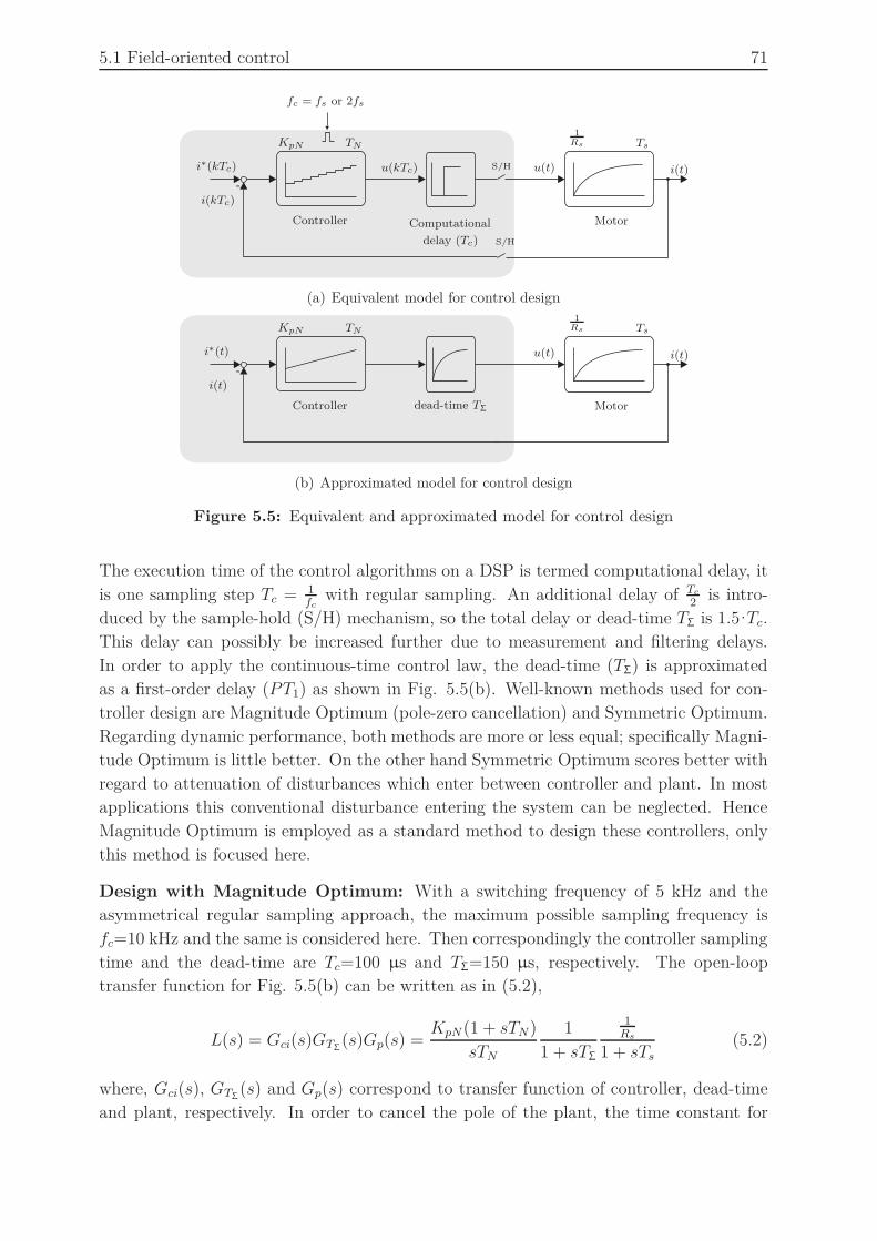
5.1 Field-oriented control 71
-
i∗(kTc)
i(kTc)
i(t)u(kTc)
KpN TN Ts1Rs
S/H
S/H
fc = fs or 2fs
u(t)
Controller MotorComputational
delay (Tc)
(a) Equivalent model for control design
-
i∗(t)
i(t)
i(t)u(t)
KpN TN Ts1Rs
Controller Motordead-time TΣ
(b) Approximated model for control design
Figure 5.5: Equivalent and approximated model for control design
The execution time of the control algorithms on a DSP is termed computational delay, it
is one sampling step Tc = 1fc
with regular sampling. An additional delay of Tc2
is intro-
duced by the sample-hold (S/H) mechanism, so the total delay or dead-time TΣ is 1.5·Tc.
This delay can possibly be increased further due to measurement and filtering delays.
In order to apply the continuous-time control law, the dead-time (TΣ) is approximated
as a first-order delay (PT1) as shown in Fig. 5.5(b). Well-known methods used for con-
troller design are Magnitude Optimum (pole-zero cancellation) and Symmetric Optimum.
Regarding dynamic performance, both methods are more or less equal; specifically Magni-
tude Optimum is little better. On the other hand Symmetric Optimum scores better with
regard to attenuation of disturbances which enter between controller and plant. In most
applications this conventional disturbance entering the system can be neglected. Hence
Magnitude Optimum is employed as a standard method to design these controllers, only
this method is focused here.
Design with Magnitude Optimum: With a switching frequency of 5 kHz and the
asymmetrical regular sampling approach, the maximum possible sampling frequency is
fc=10 kHz and the same is considered here. Then correspondingly the controller sampling
time and the dead-time are Tc=100 µs and TΣ=150 µs, respectively. The open-loop
transfer function for Fig. 5.5(b) can be written as in (5.2),
L(s) = Gci(s)GTΣ(s)Gp(s) =KpN(1 + sTN)
sTN
1
1 + sTΣ
1Rs
1 + sTs(5.2)
where, Gci(s), GTΣ(s) and Gp(s) correspond to transfer function of controller, dead-time
and plant, respectively. In order to cancel the pole of the plant, the time constant for
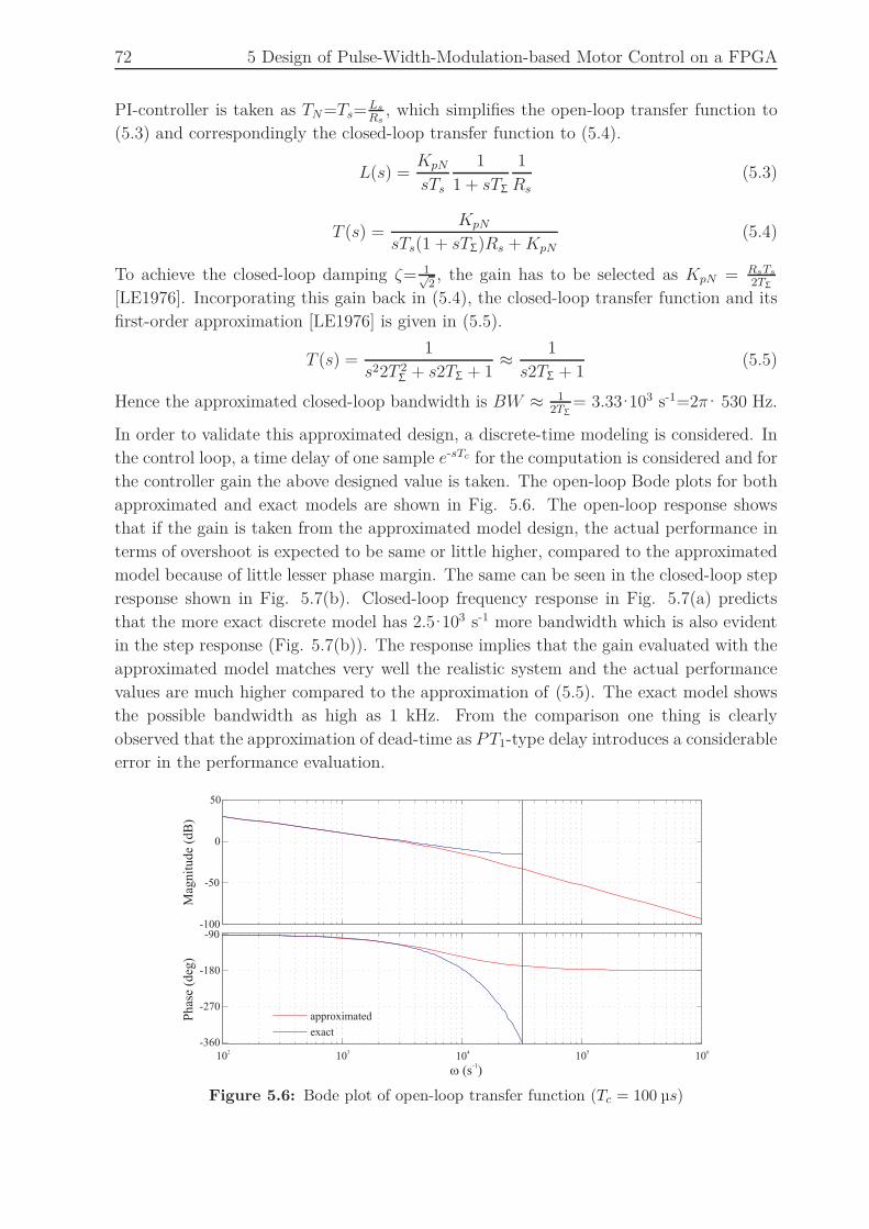
72 5 Design of Pulse-Width-Modulation-based Motor Control on a FPGA
PI-controller is taken as TN=Ts=LsRs
, which simplifies the open-loop transfer function to
(5.3) and correspondingly the closed-loop transfer function to (5.4).
L(s) =KpN
sTs
1
1 + sTΣ
1
Rs
(5.3)
T (s) =KpN
sTs(1 + sTΣ)Rs +KpN(5.4)
To achieve the closed-loop damping ζ= 1√2, the gain has to be selected as KpN = RsTs
2TΣ
[LE1976]. Incorporating this gain back in (5.4), the closed-loop transfer function and its
first-order approximation [LE1976] is given in (5.5).
T (s) =1
s22T 2Σ + s2TΣ + 1
≈1
s2TΣ + 1(5.5)
Hence the approximated closed-loop bandwidth is BW ≈ 12TΣ
= 3.33·103 s-1=2π· 530 Hz.
In order to validate this approximated design, a discrete-time modeling is considered. In
the control loop, a time delay of one sample e-sTc for the computation is considered and for
the controller gain the above designed value is taken. The open-loop Bode plots for both
approximated and exact models are shown in Fig. 5.6. The open-loop response shows
that if the gain is taken from the approximated model design, the actual performance in
terms of overshoot is expected to be same or little higher, compared to the approximated
model because of little lesser phase margin. The same can be seen in the closed-loop step
response shown in Fig. 5.7(b). Closed-loop frequency response in Fig. 5.7(a) predicts
that the more exact discrete model has 2.5·103 s-1 more bandwidth which is also evident
in the step response (Fig. 5.7(b)). The response implies that the gain evaluated with the
approximated model matches very well the realistic system and the actual performance
values are much higher compared to the approximation of (5.5). The exact model shows
the possible bandwidth as high as 1 kHz. From the comparison one thing is clearly
observed that the approximation of dead-time as PT1-type delay introduces a considerable
error in the performance evaluation.
-100
-50
0
50
Mag
nit
ude
(dB
)
102
103
104
105
106
-360
-270
-180
-90
Phas
e (d
eg)
w ( )s-1
approximated
exact
Figure 5.6: Bode plot of open-loop transfer function (Tc = 100 µs)

5.1 Field-oriented control 73
-60
-50
-40
-30
-20
-10
0
Mag
nit
ude
(dB
)
101
102
103
104
105
-450
-360
-270
-180
-90
0
Phas
e (d
eg)
approximated
exact
w ( )s-1
(a) Bode plot of closed-loop transfer function
0 0.5 1 1.5 2 2.5
x 10-3
0
0.2
0.4
0.6
0.8
1
Time (s)
Am
pli
tud
e
approximated
exact
(b) Step response of closed-loop transfer function
Figure 5.7: Closed-loop frequency and time response with Magnitude Optimum
5.1.2 Quasi-continuous control design
As it becomes apparent from the above discussion, in the regular-sampled approach, even
though the sampling rate is quite high, the bandwidth achieves hardly 1 kHz. From the
course of study it is clear that the bandwidth can only be increased by reducing the
sampling time and hence the dead-time TΣ in the control loop. This implies indirectly to
reduce the computation time in the system. Looking back to the early 1970s, most of con-
trol realization was based on analog circuits (op-amps). Such an analog implementation
does not introduce any dead-time in the system, so (5.5) indicates achievable bandwidth is
high, theoretically even infinite. However, analog implementation has its own drawbacks
such as offset, drift, non-linearity etc. and thus is not desired anymore. Hence one should
aim to achieve the performance of analog realization on a digital platform.
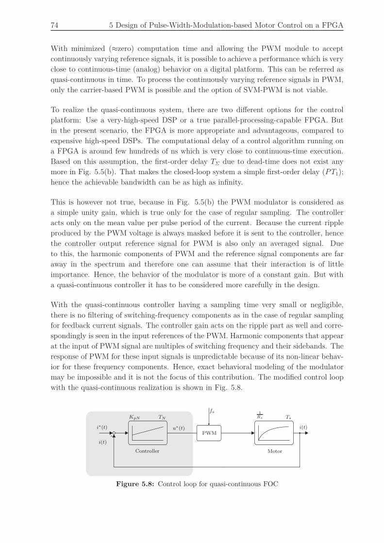
74 5 Design of Pulse-Width-Modulation-based Motor Control on a FPGA
With minimized (≈zero) computation time and allowing the PWM module to accept
continuously varying reference signals, it is possible to achieve a performance which is very
close to continuous-time (analog) behavior on a digital platform. This can be referred as
quasi-continuous in time. To process the continuously varying reference signals in PWM,
only the carrier-based PWM is possible and the option of SVM-PWM is not viable.
To realize the quasi-continuous system, there are two different options for the control
platform: Use a very-high-speed DSP or a true parallel-processing-capable FPGA. But
in the present scenario, the FPGA is more appropriate and advantageous, compared to
expensive high-speed DSPs. The computational delay of a control algorithm running on
a FPGA is around few hundreds of ns which is very close to continuous-time execution.
Based on this assumption, the first-order delay TΣ due to dead-time does not exist any
more in Fig. 5.5(b). That makes the closed-loop system a simple first-order delay (PT1);
hence the achievable bandwidth can be as high as infinity.
This is however not true, because in Fig. 5.5(b) the PWM modulator is considered as
a simple unity gain, which is true only for the case of regular sampling. The controller
acts only on the mean value per pulse period of the current. Because the current ripple
produced by the PWM voltage is always masked before it is sent to the controller, hence
the controller output reference signal for PWM is also only an averaged signal. Due
to this, the harmonic components of PWM and the reference signal components are far
away in the spectrum and therefore one can assume that their interaction is of little
importance. Hence, the behavior of the modulator is more of a constant gain. But with
a quasi-continuous controller it has to be considered more carefully in the design.
With the quasi-continuous controller having a sampling time very small or negligible,
there is no filtering of switching-frequency components as in the case of regular sampling
for feedback current signals. The controller gain acts on the ripple part as well and corre-
spondingly is seen in the input references of the PWM. Harmonic components that appear
at the input of PWM signal are multiples of switching frequency and their sidebands. The
response of PWM for these input signals is unpredictable because of its non-linear behav-
ior for these frequency components. Hence, exact behavioral modeling of the modulator
may be impossible and it is not the focus of this contribution. The modified control loop
with the quasi-continuous realization is shown in Fig. 5.8.
-
i∗(t)
i(t)
i(t)u∗(t)
KpN TN Ts1Rs
Controller Motor
PWM
fs
Figure 5.8: Control loop for quasi-continuous FOC

5.1 Field-oriented control 75
The difference to Fig. 5.5(b) is that the dead-time due to computation does not exist any
more and for simplicity the measurement delay in the feedback current is neglected.
Design criteria: Due to the presence of PWM harmonics in the feedback current, one has
to keep in mind the following important basic criteria while designing the quasi-continuous
PWM control:
1. No more than two switchings in one PWM period is allowed.
2. The reference signal for the PWM should never be forced into saturation in steady-
state operation; otherwise uncontrolled over modulation with pulse dropping would
be the consequence.
Additionally, the controller designed to satisfy the above two constraints should also
ensure that the harmonic distortion (THD) produced in the motor line currents must be
well within the allowed range.
Design procedure: The procedure adopted with the quasi-continuous time approach
is expected to be much easier because the continuous-time control laws can be applied
directly. Importantly, the designed system should satisfy the above mentioned criteria.
To meet criterion 1: No more than two switchings per PWM period can be ensured
by controlling the slope of the reference signal. Two different conditions depending on
the relative slopes between the reference and the carrier are depicted in Fig. 5.9. Fig.
5.9(a) corresponds to the condition when the slope of the reference voltage (in red) is
higher compared to that of the carrier (in blue). In this particular case it is clearly visible
that the output changeover happens four times, which basically violates the fundamental
requirement of the PWM. On the other hand, if the reference slope is ensured to be lower
compared to the carrier as depicted in Fig. 5.9(b), the changeover happens only twice in
one PWM period. Therefore, to satisfy criterion 1, the controller has to make sure that
the slope of the reference signal is always lower than the slope of the carrier.
The PI-controllers for highly dynamic applications can be approximated as high-gain
P-controllers, because the task of the integrator is only to compensate the steady error.
2 3 41
+1
-1
t
(a) Reference-voltage slope higher than carrier
21
t
+1
-1
(b) Reference-voltage slope lower than carrier
Figure 5.9: PWM output with slope of reference voltage (red) higher and lower compared to
carrier slope (blue)
76 5 Design of Pulse-Width-Modulation-based Motor Control on a FPGA
With this, the slope of the reference voltage can be computed very easily by evaluating the
slope of the control error signal. One can easily assume the slope of the current reference
signal as very small (≈zero), because it is the output of the speed/flux-controller, which
is usually slow in comparison to the current-controller output. Then it is necessary to
evaluate the product of the actual current slope caused by the PWM voltage and the
controller gain to find the reference-voltage slope. The slope of the motor current d- and
q-axis components can be computed with help of the voltage equations. Equation (5.6)
calculates the slopes for isd and isq, where usd and usq are the actual applied voltages.
The slope of these currents depends on the motor speed (or modulation index M) and the
load conditions, where M is the normalized peak value (0 < M < 1.15) of the respective
sinusoidal phase voltages M = u∗
udc/2.
isd =1
Ls[usd − Rsisd + ωLsisq]
isq =1
Ls[usq −Rsisq − ωψp + Lsisd]
(5.6)
Equation (5.6) is used to find the maximum slope in the d- and q-axis reference voltages
by multiplying with the respective controller gains (KpNd, KpNq). In order to utilize
the maximum DC-bus voltage, instantaneous “zero-sequence” or “common-mode” voltage
injection is performed [WM1991]. Hence, while calculating the individual phase reference-
voltages slope from the (d- and q-) components, the gain enhancement due to the zero-
sequence component injection has to be taken into account. The maximum allowable
slope of the input reference signals can be as high as Vdc·fs2
= Vdc100 µs
= 3.2·106 Vs-1. Based
on this maximum value, the allowable gain for both controllers can be calculated as given
below:
KpNd =3.2·106 Vs-1
Max(isd) As-1 , KpNq =3.2·106 Vs-1
Max(isq) As-1
As the denominator quantity is a function of M and isq, the current slopes and the
respective controller gain values are represented as function of these quantities in Fig.
5.10(a) and 5.10(b), respectively. It is evident that the gain values are varying as a
function of modulation index and load, represented as q-axis current in pu1. Using these
gains in the controller ensures no more than two switchings in one PWM period.
To meet criterion 2: Second criterion for the selection of the controller parameters
has to ensure that in steady-state operation the reference voltages are not driven into
saturation even for a short time. Normally with FOC the maximum possible voltage of
an inverter driving the motor is always little bigger than the rated voltage of the motor.
But, this margin voltage is only valid for the fundamental component of the reference
voltage. If the reference has a switching ripple (case with quasi-continuous control) with
a value more than the margin, then it will obviously saturate the reference voltages when
the motor is operating close to the rated speed. According to this, one can imagine
that the controller gain can be higher in the lower speed range due to higher margin to
1pu (per-unit): is normalized value with respective rated quantity

5.1 Field-oriented control 77
0 0.1 0.2 0.3 0.4 0.5 0.6 0.72.5
3
3.5
4
4.5
5x 10
4
0 0.1 0.2 0.3 0.4 0.5 0.6 0.750
60
70
80
M
isq
=0
isq
=0.25
isq
=0.5
isq
=0.75
isq
=1
i sd
(As
)-1
KpN
d(
)Ω
(a) Current slope and maximum possible gain for the d-axis controller
0 0.1 0.2 0.3 0.4 0.5 0.6 0.71
2
3
4
5x 10
4
0 0.1 0.2 0.3 0.4 0.5 0.6 0.7
60
80
100
120isq
=0
isq
=0.25
isq
=0.5
isq
=0.75
isq
=1
M
i sq
(As
)-1
Kp
Nq
()
Ω
(b) Current slope and maximum possible gain for the q-axis controller
Figure 5.10: d- and q-axis current slopes and corresponding maximum possible controller gain
saturation level, while at higher speed there is very little margin and thus relatively small
gain. In order to investigate this issue, one should have an understanding of the ripple
current as a function of speed or the modulation index M .
The PWM applies the pulse voltage to the motor, the mean value over the PWM period
being equal to the input reference voltage. The instantaneous difference between the
reference and the actual applied PWM voltage introduces the current ripple along with the
fundamental (or average value per PWM pulse period) current component. Researchers
have worked on analytical evaluation of this current ripple for loss calculations in the
motor [BS1988] [AR2009]. These papers give some clues for the ripple current to be
evaluated analytically. The ripple current in phase a can be written as in (5.7),

78 5 Design of Pulse-Width-Modulation-based Motor Control on a FPGA
∆isa =udc2Ls
∫
∆usa dt (5.7)
where ∆usa is the normalized difference voltage between the applied PWM phase-to-
neutral and the reference sinusoidal voltage (with zero-sequence voltage injected). This
voltage can be written as a function of switching signals (Sa, Sb, Sc); the switching signal
can have two states: +1 or -1.
∆usa = usa − u∗sa = f(Sa,Sb,Sc) − u∗
sa (5.8)
For the evaluation process, in (5.8) the DC-link voltage udc is assumed to be constant
and the switching-time delays of the inverter switches are neglected. The instant of
switching of these voltages can be evaluated analytically using a small iterative program
as a function of modulation index M . It is very important to mention that in the iteration
program, especially at very low modulation index, the introduction of a DC bias current is
possible. A lead function can be used to block this bias. Fig. 5.11 shows the current ripple
with the respective reference phase voltage. The reference signal is sinusoidal with zero-
sequence component injected. The plot in Fig. 5.11(a) is corresponding to M=0.5 and
Fig. 5.11(b) for M=1. The peak-peak current ripple is not constant in the whole cycle for
the respective modulation indices. The ripple will not force the reference into saturation
with higher gains at lower speeds, while gain adaptation is essential as the motor runs at
0 1 2 3 4 5 6
x 10-3
-1
0
1
Cu
rren
t (A
)
Time (s)0 1 2 3 4 5 6
x 10-3
-0.5
0
0.5
No
rmal
ized
usa
*
(a) Current ripple for M=0.5 (Udc=320 V, Ls=5.3 mH, fs
f≈29)
0 0.5 1 1.5 2 2.5 3
x 10-3
-1
-0.5
0
0.5
1
Curr
ent
(A)
Time (s)0 0.5 1 1.5 2 2.5 3
x 10-3
-1
-0.5
0
0.5
1
Norm
aliz
edu
sa
*
(b) Current ripple for M=1 (Udc=320 V, Ls=5.3 mH, fs
f≈14.5)
Figure 5.11: Current ripple with respective phase voltage for different modulation indices
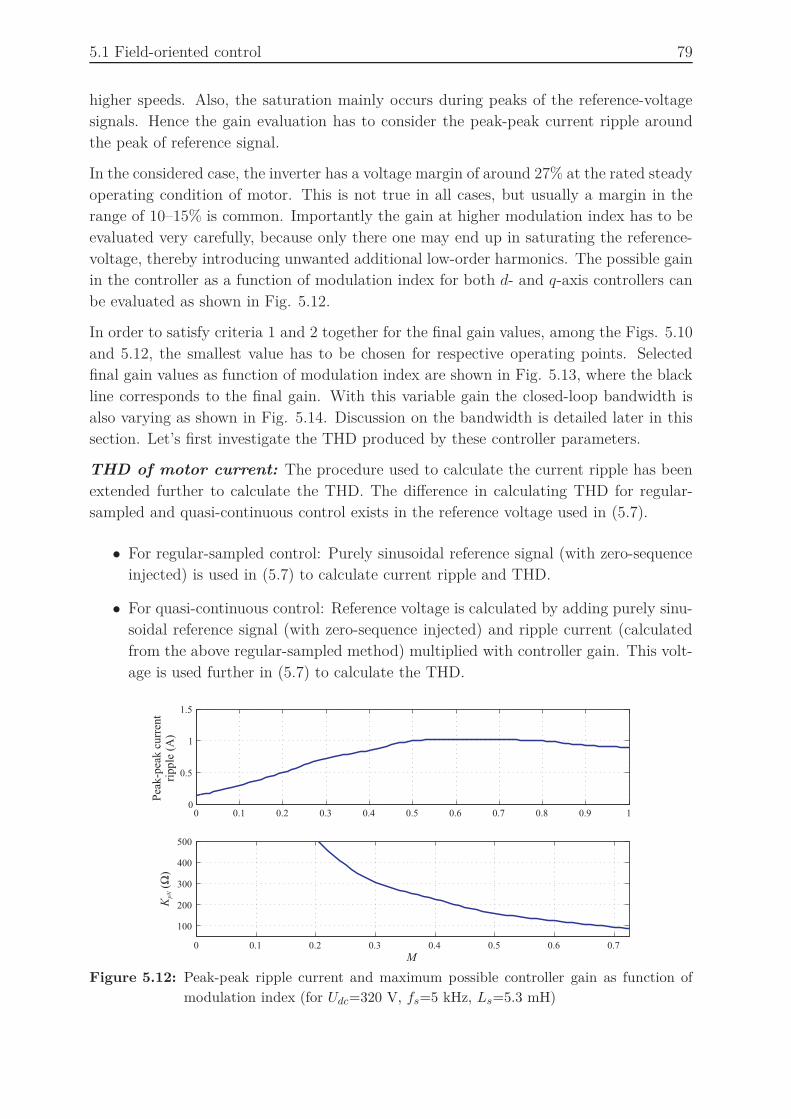
5.1 Field-oriented control 79
higher speeds. Also, the saturation mainly occurs during peaks of the reference-voltage
signals. Hence the gain evaluation has to consider the peak-peak current ripple around
the peak of reference signal.
In the considered case, the inverter has a voltage margin of around 27% at the rated steady
operating condition of motor. This is not true in all cases, but usually a margin in the
range of 10–15% is common. Importantly the gain at higher modulation index has to be
evaluated very carefully, because only there one may end up in saturating the reference-
voltage, thereby introducing unwanted additional low-order harmonics. The possible gain
in the controller as a function of modulation index for both d- and q-axis controllers can
be evaluated as shown in Fig. 5.12.
In order to satisfy criteria 1 and 2 together for the final gain values, among the Figs. 5.10
and 5.12, the smallest value has to be chosen for respective operating points. Selected
final gain values as function of modulation index are shown in Fig. 5.13, where the black
line corresponds to the final gain. With this variable gain the closed-loop bandwidth is
also varying as shown in Fig. 5.14. Discussion on the bandwidth is detailed later in this
section. Let’s first investigate the THD produced by these controller parameters.
THD of motor current: The procedure used to calculate the current ripple has been
extended further to calculate the THD. The difference in calculating THD for regular-
sampled and quasi-continuous control exists in the reference voltage used in (5.7).
• For regular-sampled control: Purely sinusoidal reference signal (with zero-sequence
injected) is used in (5.7) to calculate current ripple and THD.
• For quasi-continuous control: Reference voltage is calculated by adding purely sinu-
soidal reference signal (with zero-sequence injected) and ripple current (calculated
from the above regular-sampled method) multiplied with controller gain. This volt-
age is used further in (5.7) to calculate the THD.
0 0.1 0.2 0.3 0.4 0.5 0.6 0.7 0.8 0.9 10
0.5
1
1.5
0 0.1 0.2 0.3 0.4 0.5 0.6 0.7
100
200
300
400
500
Pea
k-p
eak
cu
rren
tri
pp
le (
A)
Kp
N(
)Ω
M
Figure 5.12: Peak-peak ripple current and maximum possible controller gain as function of
modulation index (for Udc=320 V, fs=5 kHz, Ls=5.3 mH)

80 5 Design of Pulse-Width-Modulation-based Motor Control on a FPGA
M
Kp
Nq
()
Ω
0 0.1 0.2 0.3 0.4 0.5 0.6 0.750
100
150
0 0.1 0.2 0.3 0.4 0.5 0.6 0.750
100
150
Kp
Nd
()
Ωisq
isq
Figure 5.13: Final gain selection for the controller as a function of modulation index M and
load
The THD curves from both methods are presented in Fig. 5.15. The difference is not
at all considerable, it indicates that the PWM attenuates switching harmonic reference
components to a great level. The control design being based on the above procedure, it
is still possible to approximate the PWM behavior as a constant gain for the steady-state
case. With this assumption, the closed-loop current controller is reduced to a first-order
delay.
Enhancement of dynamics using feedback delay: The regular-sampled control dis-
cussed above does not consider any delay in the feedback signal. In real systems, one
cannot avoid these delays. Any additional delay will reduce the damping of the closed-
loop system and hence reduce the achievable performance. In contrast to this, in quasi-
continuous control addition of delay in the form of low-pass filtering will enhance the
performance in terms of higher dynamics and lower THD. It is hard to believe because
one always tend to think that any additional delay in feedback will reduce the margin
for the dynamics. Here with the quasi-continuous approach, the closed current loop is
reduced to a simple first-order delay which implies that the phase margin is equal to
90
. In order to achieve better dynamics, damping has to be reduced hence the margin
0 0.1 0.2 0.3 0.4 0.5 0.6 0.7 0.8 0.9 10
1000
2000
3000
4000
M
Ban
dw
idth
(H
z)
q-axis controller
d-axis controller
Figure 5.14: Achievable closed-loop bandwidth of controller (Udc=320 V, Ls=5.3 mH, fs=5
kHz)
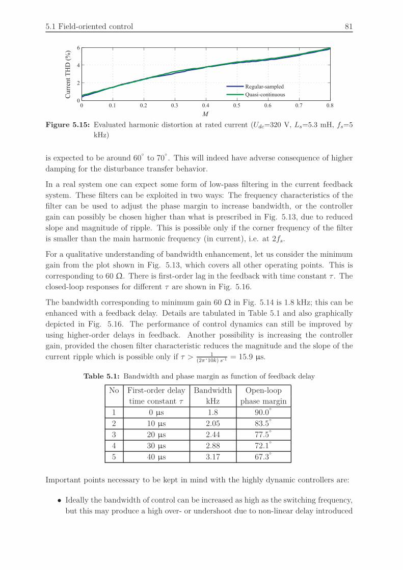
5.1 Field-oriented control 81
0 0.1 0.2 0.3 0.4 0.5 0.6 0.7 0.80
2
4
6
M
Regular-sampled
Quasi-continuousCu
rren
tT
HD
(%
)
Figure 5.15: Evaluated harmonic distortion at rated current (Udc=320 V, Ls=5.3 mH, fs=5
kHz)
is expected to be around 60
to 70
. This will indeed have adverse consequence of higher
damping for the disturbance transfer behavior.
In a real system one can expect some form of low-pass filtering in the current feedback
system. These filters can be exploited in two ways: The frequency characteristics of the
filter can be used to adjust the phase margin to increase bandwidth, or the controller
gain can possibly be chosen higher than what is prescribed in Fig. 5.13, due to reduced
slope and magnitude of ripple. This is possible only if the corner frequency of the filter
is smaller than the main harmonic frequency (in current), i.e. at 2fs.
For a qualitative understanding of bandwidth enhancement, let us consider the minimum
gain from the plot shown in Fig. 5.13, which covers all other operating points. This is
corresponding to 60 Ω. There is first-order lag in the feedback with time constant τ . The
closed-loop responses for different τ are shown in Fig. 5.16.
The bandwidth corresponding to minimum gain 60 Ω in Fig. 5.14 is 1.8 kHz; this can be
enhanced with a feedback delay. Details are tabulated in Table 5.1 and also graphically
depicted in Fig. 5.16. The performance of control dynamics can still be improved by
using higher-order delays in feedback. Another possibility is increasing the controller
gain, provided the chosen filter characteristic reduces the magnitude and the slope of the
current ripple which is possible only if τ > 1(2π·10k) s-1 = 15.9 µs.
Table 5.1: Bandwidth and phase margin as function of feedback delay
No First-order delay Bandwidth Open-loop
time constant τ kHz phase margin
1 0 µs 1.8 90.0
2 10 µs 2.05 83.5
3 20 µs 2.44 77.5
4 30 µs 2.88 72.1
5 40 µs 3.17 67.3
Important points necessary to be kept in mind with the highly dynamic controllers are:
• Ideally the bandwidth of control can be increased as high as the switching frequency,
but this may produce a high over- or undershoot due to non-linear delay introduced

82 5 Design of Pulse-Width-Modulation-based Motor Control on a FPGA
by the PWM for transient step inputs. The delay is predominantly increased, as
bandwidth approaches switching frequency.
• In practice, PI-controller outputs have saturation to limit the maximum value. For
large control error (usually occurring with step command), the output is satu-
rated immediately and hence the full “small-signal” dynamic capabilities cannot
be demonstrated.
0 0.5 1 1.5 2 2.5 3 3.5 4 4.5 5
x 10-4
0
0.2
0.4
0.6
0.8
1
t (s)
Am
pli
tud
e
τ= 20 µs
τ= 10 µs
τ= 40 µs
τ= 30 µs
τ
(a) Step response with feedback delay
-15
-10
-5
0
5
Mag
nit
ud
e (d
B)
103
104
0
Ph
ase
ω (s )-1
τ= 20 µs
τ= 10 µs
τ= 40 µs
τ= 30 µs
- π/2
- π/3
- π/6
τ
τ
(b) Bode plot of closed-loop transfer function
Figure 5.16: Closed-loop response with first-order delay (τ) in feedback
5.1.3 Implementation
Fig. 5.17 shows the complete block schematic of the structure implemented on the FPGA
with important blocks marked. The System-Generator tool from Xilinx has been used for
implementation.

5.1 Field-oriented control 83
Th
eta
co
s(e
)
sin
(e)
sp
ee
d
sin
/cos/w
Lim
it
Isq
*
Isq
Isd
W
usq
*
q-a
xis
Contr
olle
r+
feed forw
ard
term
s
Lim
it
Isd
Isd
*
Isq
W
usd
*
d-a
xis
Contr
olle
r+
feed forw
ard
term
s
Ou
t
cH
Ou
t
bHO
ut
aH
Init_
Virte
x2
Pro
.m
Da
ta_
1
Da
ta_
2
Softscope
In
Sig
ma_D
elta_C
LK
bitstr
ea
m I
sa
bitstr
ea
m I
sb
bitstr
ea
m I
sc
Clk
Is_
Alp
ha
Is_
Be
ta
Sig
ma D
elta F
ilter
In Positio
n d
ata
0
Isq*
0
Isd*
IsA
lph
a
Is B
eta
co
s(e
)
sin
(e)
Isq
Isd
Coord
inate
Tr.
Vsq
*
Vsd
*
Sin
e
Co
se
us
Alp
ha
*
us B
eta
*
Coord
inate
Tr.
ua
*
ub
*
uc*
Sa
Sb
Sc
Com
parison w
ith C
arr
ier
In Bitstr
eam
Isc
In Bitstr
eam
Isb
In Bitstr
eam
Isa
us
Alp
ha
*
us B
lph
a*
Sa
tura
tio
n
usa
**
usb
**
usc**
Alp
ha/B
eta
to a
,b,c
additio
n o
f "n
ull"
com
p.
Da
taP
osis
tio
n
Abs. E
ncoder
SS
I
Syste
mG
en
era
tor
Dat
a ac
quis
itio
nC
ontr
oll
erM
onit
ori
ng
PW
M a
nd s
wit
chin
g s
ignal
s
Figure 5.17: Implementation using System-Generator tool on Matlab-Simulink platform
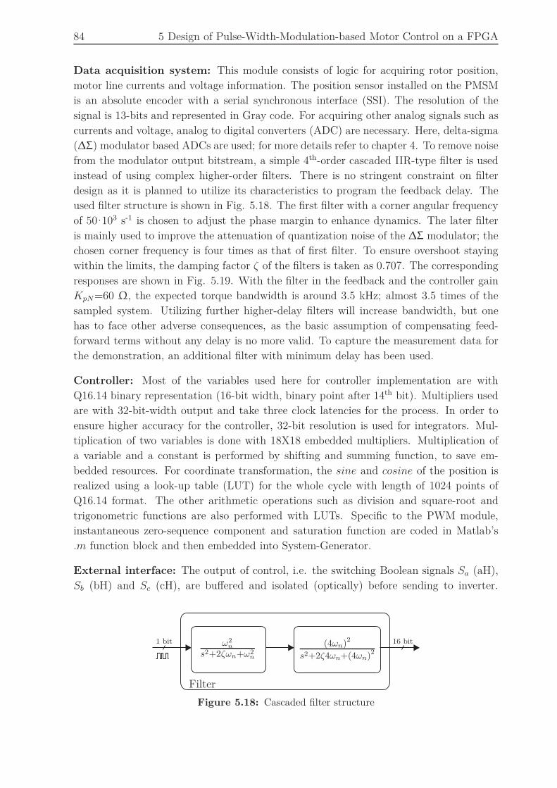
84 5 Design of Pulse-Width-Modulation-based Motor Control on a FPGA
Data acquisition system: This module consists of logic for acquiring rotor position,
motor line currents and voltage information. The position sensor installed on the PMSM
is an absolute encoder with a serial synchronous interface (SSI). The resolution of the
signal is 13-bits and represented in Gray code. For acquiring other analog signals such as
currents and voltage, analog to digital converters (ADC) are necessary. Here, delta-sigma
(∆Σ) modulator based ADCs are used; for more details refer to chapter 4. To remove noise
from the modulator output bitstream, a simple 4th-order cascaded IIR-type filter is used
instead of using complex higher-order filters. There is no stringent constraint on filter
design as it is planned to utilize its characteristics to program the feedback delay. The
used filter structure is shown in Fig. 5.18. The first filter with a corner angular frequency
of 50·103 s-1 is chosen to adjust the phase margin to enhance dynamics. The later filter
is mainly used to improve the attenuation of quantization noise of the ∆Σ modulator; the
chosen corner frequency is four times as that of first filter. To ensure overshoot staying
within the limits, the damping factor ζ of the filters is taken as 0.707. The corresponding
responses are shown in Fig. 5.19. With the filter in the feedback and the controller gain
KpN=60 Ω, the expected torque bandwidth is around 3.5 kHz; almost 3.5 times of the
sampled system. Utilizing further higher-delay filters will increase bandwidth, but one
has to face other adverse consequences, as the basic assumption of compensating feed-
forward terms without any delay is no more valid. To capture the measurement data for
the demonstration, an additional filter with minimum delay has been used.
Controller: Most of the variables used here for controller implementation are with
Q16.14 binary representation (16-bit width, binary point after 14th bit). Multipliers used
are with 32-bit-width output and take three clock latencies for the process. In order to
ensure higher accuracy for the controller, 32-bit resolution is used for integrators. Mul-
tiplication of two variables is done with 18X18 embedded multipliers. Multiplication of
a variable and a constant is performed by shifting and summing function, to save em-
bedded resources. For coordinate transformation, the sine and cosine of the position is
realized using a look-up table (LUT) for the whole cycle with length of 1024 points of
Q16.14 format. The other arithmetic operations such as division and square-root and
trigonometric functions are also performed with LUTs. Specific to the PWM module,
instantaneous zero-sequence component and saturation function are coded in Matlab’s
.m function block and then embedded into System-Generator.
External interface: The output of control, i.e. the switching Boolean signals Sa (aH),
Sb (bH) and Sc (cH), are buffered and isolated (optically) before sending to inverter.
1 bit 16 bitω2
n
s2+2ζωn+ω2n
Filter
(4ωn)2
s2+2ζ4ωn+(4ωn)2
Figure 5.18: Cascaded filter structure

5.1 Field-oriented control 85
- π
-200
-150
-100
-50
0
50
Mag
nit
ude
(dB
)
103
104
105
106
107
0
0 0.5 1 1.5
x 10-4
0
0.2
0.4
0.6
0.8
1
1.2
1.4
t (s)
Am
pli
tude
Phas
e
- 2π
- π/2
- 3π/2
ω (s )-1
Figure 5.19: Frequency and time response of filter
For data monitoring which is helpful in debugging a soft-scope is built on the FPGA.
The trigger for data storage on the FPGA and transfer of data from there to the PC is
performed using a serial RS-232 communication as seen in Fig. 5.17.
Space characterization: The amount of hardware required to map the compiled logic
on the FPGA is characterized by the number of slices occupied. The efficiency of the
mapping process is measured based on how good the resources of the slices are utilized.
The FPGA device used to map the logic is Xilinx Virtex-2P-XC2VP30. The details of the
hardware requirement are tabulated in Table. 5.2. The total time taken for the execution
of the FOC logic is around 720 ns (18 latencies), the estimation needs 480 ns (12 latencies)
and the controller 240 ns (6 latencies).
5.1.4 Experimental validation
To investigate the control performance, the test-bench setup can either be operated in
constant-speed or in constant-torque mode by means of the load-machine control. As the
focus of investigation is mainly on the regulation of torque and flux, the evaluation with
a constant-speed operation of the load machine is more suitable. The test bench consists
of PMSM and induction machine as load, the details are given in Appendix A.1. The
induction machine is operated in speed-controlled mode with the help of a GUI application
provided by the manufacturer.
Table 5.2: Space characterization of implementation (LUT: Look-Up-Table, FF: Flip-Flop)
Control Slices LUT FF Block RAM Multipliers
FOC 3325 5996 2195 31 16
24% 21% 8% 22% 11%

86 5 Design of Pulse-Width-Modulation-based Motor Control on a FPGA
0.014 0.015 0.016 0.017 0.018 0.019 0.02
-150
-100
-50
0
50
100
150
Vo
ltag
e (V
)
Time (s)
Figure 5.20: PWM carrier and reference voltage for quasi-continuous PWM controls (fs=5
kHz, f=166 Hz, Udc=320 V)
The basic idea of continuously varying reference-voltages applied to the PWM module is
shown in Fig. 5.20. The frequency of the carrier shown in red is 5 kHz and the reference
in black. The reference signal has the mentioned instantaneous zero-sequence component
along with the controller output reference signal. Transients like step torque input can
saturate the reference voltages. But that mainly depends on the change in magnitude of
step and the operating speed. The control performance discussed in section 5.1.2 is with
the presumption of unsaturated reference voltages (small-signal behavior). Dynamics of
control under such operating conditions are shown in Fig. 5.21, with the motor operating
at zero speed and a small torque step command given. Increase in the operating speed or
higher torque step command will saturate the output voltage of the controller immediately.
E.g. when the motor is operating at zero speed and the rated torque step command is
applied, it is observed that the reference voltage is saturated immediately, as evident from
Fig. 5.22. Similarly in Fig. 5.23, saturation of reference voltage is shown for the motor
operating at 0.85 pu of rated speed.
The q- and d-axis current responses during transients give an idea of the dynamic perfor-
mance of the controller. They are shown in Fig. 5.24 for the unsaturated voltage condition.
In this figure, the blue-lined plot represents the theoretical continuous behavior of the ac-
tual experimental setup, corresponding to a bandwidth of 3.5 kHz. Experimental q-axis
current response matches very closely to the theoretical continuous behavior. The timing
of response in Fig. 5.24 may vary around these, depending on the instant of transient
and carrier signal position. With regard to d-axis current control, a transient in current
is visible even when output voltage is not saturated. This small change in current is
because of delayed compensation of feed-forward terms, due to the current measurement
filter. Basically there the fundamental assumption is violated in the controller design.
Measured currents in Fig. 5.24 have small high-frequency noise, which is caused by the
quantization noise of the ADC.
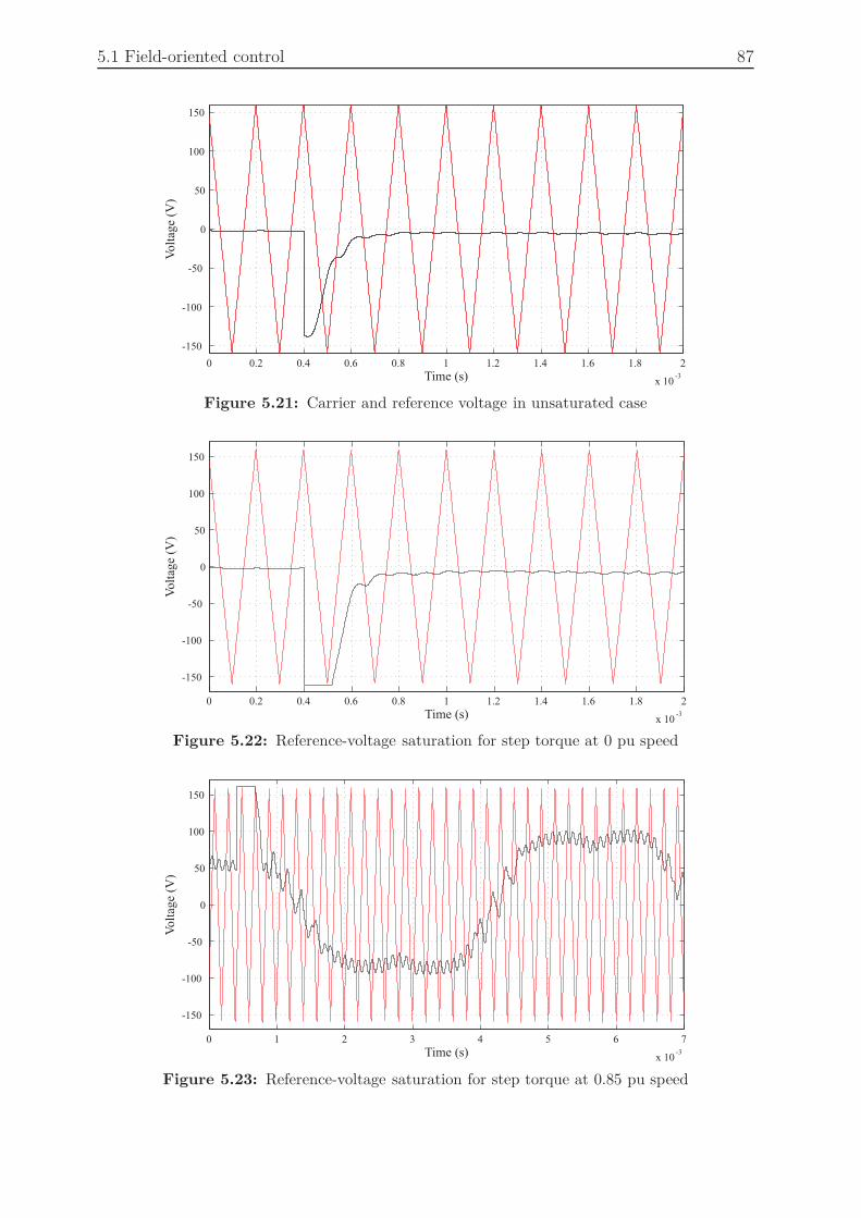
5.1 Field-oriented control 87
0 0.2 0.4 0.6 0.8 1 1.2 1.4 1.6 1.8 2
x 10-3
-150
-100
-50
0
50
100
150
Volt
age
(V)
Time (s)
Figure 5.21: Carrier and reference voltage in unsaturated case
0 0.2 0.4 0.6 0.8 1 1.2 1.4 1.6 1.8 2
x 10-3
-150
-100
-50
0
50
100
150
Volt
age
(V)
Time (s)
Figure 5.22: Reference-voltage saturation for step torque at 0 pu speed
0 1 2 3 4 5 6 7
x 10-3
-150
-100
-50
0
50
100
150
Volt
age
(V)
Time (s)
Figure 5.23: Reference-voltage saturation for step torque at 0.85 pu speed

88 5 Design of Pulse-Width-Modulation-based Motor Control on a FPGA
0 0.1 0.2 0.3 0.4 0.5 0.6 0.7 0.8 0.9 1
x 10-3
0
0.7
1.4
2.1
2.8
3.5
4.2
Cu
rren
t (A
)Reference
Actual
Ideal
0 0.1 0.2 0.3 0.4 0.5 0.6 0.7 0.8 0.9 1
x 10-3
-1.4
-0.7
0
0.7
1.4
Cu
rren
t (A
)
Time (s)
Reference
Actual
Figure 5.24: q- and d-axis current responses of FOC under unsaturated condition (0 pu speed)
0 0.1 0.2 0.3 0.4 0.5 0.6 0.7 0.8 0.9 1
x 10-3
0
1.4
2.8
4.2
5.6
7
8.4
Cu
rren
t (A
)
Reference
Actual
0 0.1 0.2 0.3 0.4 0.5 0.6 0.7 0.8 0.9 1
x 10-3
-1.4
-0.7
0
0.7
1.4
Cu
rren
t (A
)
Time (s)
Reference
Actual
Figure 5.25: q- and d-axis current response of FOC under saturated condition (0.16 pu speed)
Plots in Fig. 5.25 show q- and d-axis current responses during saturated voltage condition.
The transient time is clearly longer than in the unsaturated case (Fig 5.24). With regard
to d-axis current regulation, the performance is poor, especially for this case. It is mainly
due to halted integrators in the PI-controllers, which are not reacting upon the control
error. Regarding finally the harmonic distortion, the experimentally evaluated THD at
rated load condition is compared with the theoretically (Fig. 5.15) calculated values as
shown in Fig. 5.26, indeed matching very well.
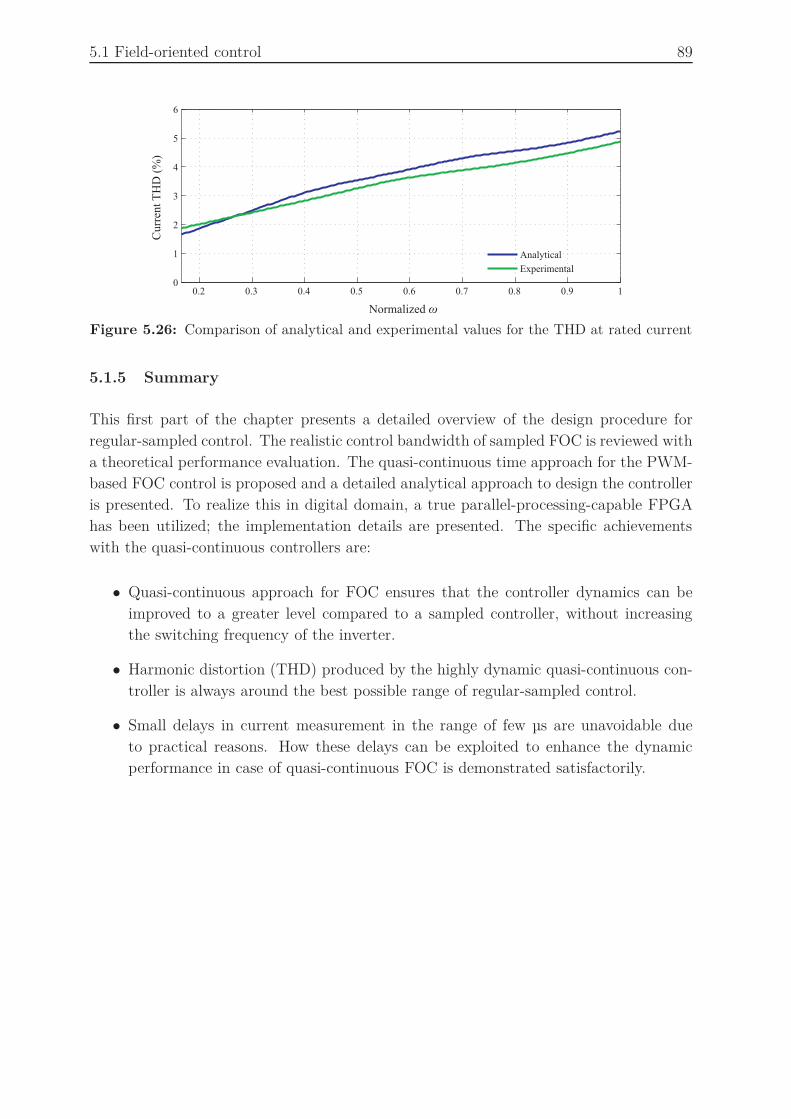
5.1 Field-oriented control 89
Curr
ent
TH
D (
%)
0.2 0.3 0.4 0.5 0.6 0.7 0.8 0.9 10
1
2
3
4
5
6
Analytical
Experimental
Normalized ω
Figure 5.26: Comparison of analytical and experimental values for the THD at rated current
5.1.5 Summary
This first part of the chapter presents a detailed overview of the design procedure for
regular-sampled control. The realistic control bandwidth of sampled FOC is reviewed with
a theoretical performance evaluation. The quasi-continuous time approach for the PWM-
based FOC control is proposed and a detailed analytical approach to design the controller
is presented. To realize this in digital domain, a true parallel-processing-capable FPGA
has been utilized; the implementation details are presented. The specific achievements
with the quasi-continuous controllers are:
• Quasi-continuous approach for FOC ensures that the controller dynamics can be
improved to a greater level compared to a sampled controller, without increasing
the switching frequency of the inverter.
• Harmonic distortion (THD) produced by the highly dynamic quasi-continuous con-
troller is always around the best possible range of regular-sampled control.
• Small delays in current measurement in the range of few µs are unavoidable due
to practical reasons. How these delays can be exploited to enhance the dynamic
performance in case of quasi-continuous FOC is demonstrated satisfactorily.
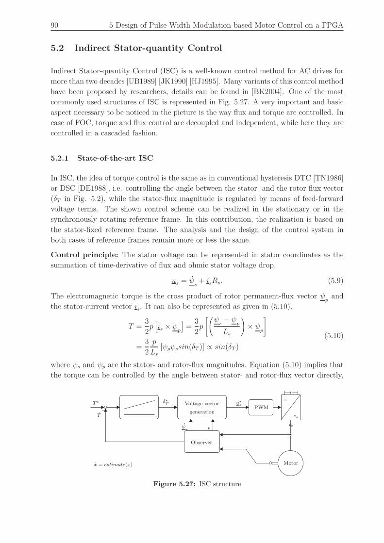
90 5 Design of Pulse-Width-Modulation-based Motor Control on a FPGA
5.2 Indirect Stator-quantity Control
Indirect Stator-quantity Control (ISC) is a well-known control method for AC drives for
more than two decades [UB1989] [JK1990] [HJ1995]. Many variants of this control method
have been proposed by researchers, details can be found in [BK2004]. One of the most
commonly used structures of ISC is represented in Fig. 5.27. A very important and basic
aspect necessary to be noticed in the picture is the way flux and torque are controlled. In
case of FOC, torque and flux control are decoupled and independent, while here they are
controlled in a cascaded fashion.
5.2.1 State-of-the-art ISC
In ISC, the idea of torque control is the same as in conventional hysteresis DTC [TN1986]
or DSC [DE1988], i.e. controlling the angle between the stator- and the rotor-flux vector
(δT in Fig. 5.2), while the stator-flux magnitude is regulated by means of feed-forward
voltage terms. The shown control scheme can be realized in the stationary or in the
synchronously rotating reference frame. In this contribution, the realization is based on
the stator-fixed reference frame. The analysis and the design of the control system in
both cases of reference frames remain more or less the same.
Control principle: The stator voltage can be represented in stator coordinates as the
summation of time-derivative of flux and ohmic stator voltage drop,
us = ψs
+ isRs. (5.9)
The electromagnetic torque is the cross product of rotor permanent-flux vector ψp
and
the stator-current vector is. It can also be represented as given in (5.10).
T =3
2p[
is × ψp
]
=3
2p
[(ψs
− ψp
Ls
)
× ψp
]
=3
2
p
Ls[ψpψssin(δT )] ∝ sin(δT )
(5.10)
where ψs and ψp are the stator- and rotor-flux magnitudes. Equation (5.10) implies that
the torque can be controlled by the angle between stator- and rotor-flux vector directly,
-
T ∗
T
u∗
sδ∗
T
ψs ǫ
Voltage vector
generation
Observer
Motor
PWM
x = estimate(x)
Figure 5.27: ISC structure
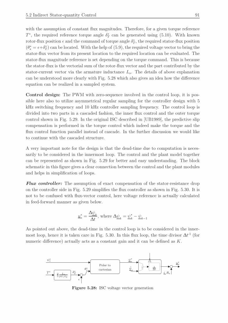
5.2 Indirect Stator-quantity Control 91
with the assumption of constant flux magnitudes. Therefore, for a given torque reference
T ∗, the required reference torque angle δ∗T can be generated using (5.10). With known
rotor-flux position ǫ and the command of torque angle δ∗T , the required stator-flux position
(θ∗s = ǫ+δ∗
T ) can be located. With the help of (5.9), the required voltage vector to bring the
stator-flux vector from its present location to the required location can be evaluated. The
stator-flux magnitude reference is set depending on the torque command. This is because
the stator-flux is the vectorial sum of the rotor-flux vector and the part contributed by the
stator-current vector via the armature inductance Ls. The details of above explanation
can be understood more clearly with Fig. 5.28 which also gives an idea how the difference
equation can be realized in a sampled system.
Control design: The PWM with zero-sequence involved in the control loop, it is pos-
sible here also to utilize asymmetrical regular sampling for the controller design with 5
kHz switching frequency and 10 kHz controller sampling frequency. The control loop is
divided into two parts in a cascaded fashion, the inner flux control and the outer torque
control shown in Fig. 5.29. In the original ISC described in [UB1989], the predictive slip
compensation is performed in the torque control which indeed make the torque and the
flux control function parallel instead of cascade. In the further discussion we would like
to continue with the cascaded structure.
A very important note for the design is that the dead-time due to computation is neces-
sarily to be considered in the innermost loop. The control and the plant model together
can be represented as shown in Fig. 5.29 for better and easy understanding. The block
schematic in this figure gives a clear connection between the control and the plant modules
and helps in simplification of loops.
Flux controller: The assumption of exact compensation of the stator-resistance drop
on the controller side in Fig. 5.29 simplifies the flux controller as shown in Fig. 5.30. It is
not to be confused with flux-vector control, here voltage reference is actually calculated
in feed-forward manner as given below.
u∗s =
∆ψk
∆t, where ∆ψ
k= ψ∗
k− ψ
k−1
As pointed out above, the dead-time in the control loop is to be considered in the inner-
most loop, hence it is taken care in Fig. 5.30. In this flux loop, the time divisor ∆t-1 (for
numeric difference) actually acts as a constant gain and it can be defined as K.
-
T ∗
ǫ
θ∗
s
ψ∗
su∗
s
δ∗
T
ψ∗
s
ψs
isRs
Polar to
cartesian
23
Ls
pψsψp
1∆t
Figure 5.28: ISC voltage vector generation
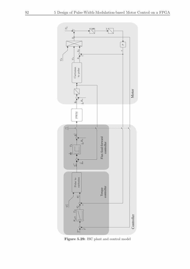
92 5 Design of Pulse-Width-Modulation-based Motor Control on a FPGA
-- M
oto
r
Flu
x f
eed
-fo
rwar
dco
ntr
oll
er
To
rqu
eco
ntr
oll
er
-
Contr
oll
er
-
-
T∗
T
TTN
KpN
ψs
i sRs
i sRs
u∗ s
us
δ∗ T
Pola
rto
Cart
esia
n
top
ola
rca
rtes
ian
ǫ
ǫ
ǫ
θ∗ s
1 J
ψ∗ s
1∆t
TΣ
TL
ψp ψs θ s
δ TP
WM
ω
p
ψ∗ s
Figure 5.29: ISC plant and control model
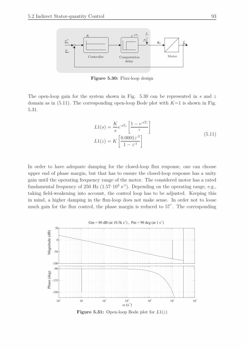
5.2 Indirect Stator-quantity Control 93
-
ψ∗
s
ψs
ψs
us
K
Controller Computationdelay
e-sTcfc
Motor
Figure 5.30: Flux-loop design
The open-loop gain for the system shown in Fig. 5.30 can be represented in s and z
domain as in (5.11). The corresponding open-loop Bode plot with K=1 is shown in Fig.
5.31.
L1(s) =K
se-sTc
[
1 − e-sTc
s
]
L1(z) = K
[
0.0001z-2
1 − z-1
] (5.11)
In order to have adequate damping for the closed-loop flux response, one can choose
upper end of phase margin, but that has to ensure the closed-loop response has a unity
gain until the operating frequency range of the motor. The considered motor has a rated
fundamental frequency of 250 Hz (1.57·103 s-1). Depending on the operating range, e.g.,
taking field-weakening into account, the control loop has to be adjusted. Keeping this
in mind, a higher damping in the flux-loop does not make sense. In order not to loose
much gain for the flux control, the phase margin is reduced to 57
. The corresponding
-100
-50
0
50
Mag
nit
ude
(dB
)
10-1
10 101
102
103
104
105
-180
-135
-90
Phas
e (d
eg)
Gm = 80 dB (at 10.5k s ) , Pm = 90 deg (at 1 s )-1 -1
ω (s )-1
Figure 5.31: Open-loop Bode plot for L1(z)

94 5 Design of Pulse-Width-Modulation-based Motor Control on a FPGA
gain K for this phase margin is 3550 s-1, i.e. approximately ∆t=280 µs. With this gain
the closed-loop transfer function is found as in (5.12).
T1(z) =0.355z-2
1 − z-1 + 0.355z-2(5.12)
Bode diagram and step response for the transfer function (5.12) are shown in Fig. 5.32.
In the frequency plot, the closed-loop bandwidth for the flux-loop is observed as high as
8.5·103 s-1 or 2π·1.35 kHz. The overshoot observed in the step response is around 8%,
because of non-conservative phase margin considered in the design.
Torque-controller design: From Fig. 5.28 it is clearly visible that no additional torque
controller would be necessary, provided one can construct the reference torque angle
perfectly from the reference torque and the reference flux vector is regulated without any
delay. If these two criteria are met, the output of the speed controller or the independent
torque reference can directly be used to drive the flux control. But that is not truly
the case, because the flux-loop dynamics is finite and therefore cannot ensure the proper
regulation of the reference angle. Hence there always exists a difference between the
actual and the reference angle. Also the quality of torque regulation is highly dependent
on the construction of the reference torque angle. With ideal assumptions it may work,
but usually in practice to ensure reliable torque regulation an additional torque-controller
is preferred at the cost of reduced closed-loop torque dynamics.
For design, the compensation of gain factors such as stator- and rotor-flux magnitudes in
the controller is assumed to be exact as of the plant values. With these assumptions the
plant for the torque-controller design is simply T1(z) which is given in (5.12). By looking
at the Bode plot (Fig. 5.32) and the transfer function T1(z), it seems that a simple
PI-controller with an appropriate time constant will meet the performance requirements.
The reset time constant of the PI-controller is chosen same as the corner frequency of
-20
-15
-10
-5
0
5
Mag
nit
ud
e (d
B)
-450
-360
-270
-180
-90
0
Ph
ase
(deg
)
0 0.5 1 1.5 2 2.5
x 10-3
0
0.2
0.4
0.6
0.8
1
Time (s)
Am
pli
tud
e
ω (s )-1
104
105
103
102
Figure 5.32: Frequency and time response of closed-loop flux-controller

5.2 Indirect Stator-quantity Control 95
the double pole of the flux-loop transfer function T1(z). Then, the open-loop transfer
function for the complete torque loop can be given as in (5.13). To avoid any additional
sampling delay, the integrator of the torque PI-controller is discretized using the bilinear
or Tustin’s approximation. It is necessary because computation delay and sampling are
already included in the design of the flux control.
L2(z) =
[
KpN +KpN
TN
Tc2
(
1 + z-1
1 − z-1)
)]
T1(z) (5.13)
With KpN=1 and TN= 18·103 s-1 =125 µs, the open-loop Bode response is shown in Fig. 5.33.
In order to achieve a good compromise between closed-loop bandwidth and damping, the
phase margin is chosen as 55
, while the corresponding gain is KpN=0.31. With this gain,
the expected closed-loop response in frequency and time domain is shown in Fig. 5.34. The
closed-loop torque bandwidth is around 6.5·103 s-1 and the overshoot observed in the step
response is close to 6%. The bandwidth is almost the same as that of sampled FOC but
the overshoot is higher in comparison. It is understandable, because the considered ISC
structure has a cascade of two controllers, while FOC has independent single controllers.
5.2.2 Quasi-continuous control design
A detailed introduction of the quasi-continuous control has already been given in section
5.1.2. To design the controller, it is required to consider the similar criteria defined
for FOC, due to the presence of PWM in the loop. Unlike FOC, in the proposed ISC
the torque is controlled via the flux-control loop in a cascaded fashion. Similar to the
above sampled control, here also controllers are considered one after the other for the
design procedure. Quasi-continuous FOC design has focused mainly on the current ripple
introduced by the PWM voltage at the motor terminals. However, ISC does not have
any particular controllers which act on the current, instead the controllers acting on the
-20
0
20
40
60
Mag
nit
ude
(dB
)
-450
-360
-270
-180
-90
0
90
Phas
e (d
eg)
Flux loop T1(z)
Torque Controller
Torque Open-loop
ω (s )-1
102
103
104
105
Figure 5.33: Bode plot for open-loop torque transfer function

96 5 Design of Pulse-Width-Modulation-based Motor Control on a FPGA
-30
-25
-20
-15
-10
-5
0
Mag
nit
ude
(dB
)
-450
-360
-270
-180
-90
0
Phas
e (d
eg)
0 0.5 1 1.5 2 2.5
x 10-3
0
0.2
0.4
0.6
0.8
1
Am
pli
tude
Time (s)ω (s )-1
104
105
103
102
Figure 5.34: Frequency and time response of closed-loop torque control
torque and flux have ripple introduced indirectly by the PWM voltage. In order to make
the analysis simpler, the torque and the flux ripple (which will be used in the design
procedure) can be defined as a function of the current ripple as in (5.14) and (5.15),
respectively:
∆T =[3
2pψp
]
∆isq (5.14)
∆ψs
=∫
(us − u∗s) dt = Ls∆is (5.15)
Control design: The flux-controller gain K calculated in the previous section was auto-
matically restricted by the controller dead-time. Due to the neglection of this dead-time
(because it is too small) in the quasi-continuous approach, the inner flux loop turns out
to be a simple first-order delay. Ideally the gain for K is infinite, but to have flexibility in
the torque-controller design one can fix the gain of the flux loop such that it gives just the
adequate performance to regulate the alternating flux references. The rated frequency of
the motor is 250 Hz. With field-weakening considered the flux loop is designed such that
it gives a bandwidth around 1 kHz. The corresponding gain is
K =1
150 µs= 6666.66 s-1 .
To make the design approach further simpler, the torque-controller time constant TN is
selected as the time constant of the flux-loop, i.e. 150 µs.
The slope and the peak-peak ripple of the reference voltages are the important factors
for control design. Both these factors are finally decided in the flux controller. Ripple
and slope of the reference and the actual signal at the input of the flux control have to
be evaluated, to find finally the factors for the reference voltages. Unlike in FOC where
the reference currents were assumed as free of ripple and slope, in this case the input
flux reference cannot be considered as ripple-free, because it is the output of the torque
controller. The proportional and the integral gains of the torque controller act on the
actual torque ripple (ref. (5.14)) and the ripple carries this further in the reference torque
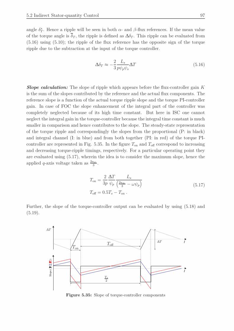
5.2 Indirect Stator-quantity Control 97
angle δ∗T . Hence a ripple will be seen in both α- and β-flux references. If the mean value
of the torque angle is δT , the ripple is defined as ∆δT . This ripple can be evaluated from
(5.16) using (5.10); the ripple of the flux reference has the opposite sign of the torque
ripple due to the subtraction at the input of the torque controller.
∆δT ≈ −2
3
Lspψpψs
∆T (5.16)
Slope calculation: The slope of ripple which appears before the flux-controller gain K
is the sum of the slopes contributed by the reference and the actual flux components. The
reference slope is a function of the actual torque ripple slope and the torque PI-controller
gain. In case of FOC the slope enhancement of the integral part of the controller was
completely neglected because of its high time constant. But here in ISC one cannot
neglect the integral gain in the torque-controller because the integral time constant is much
smaller in comparison and hence contributes to the slope. The steady-state representation
of the torque ripple and correspondingly the slopes from the proportional (P: in black)
and integral channel (I: in blue) and from both together (PI: in red) of the torque PI-
controller are represented in Fig. 5.35. In the figure Ton and Toff correspond to increasing
and decreasing torque-ripple timings, respectively. For a particular operating point they
are evaluated using (5.17), wherein the idea is to consider the maximum slope, hence the
applied q-axis voltage taken as 2udc3
.
Ton =2
3p
∆T
ψp
Ls(
2udc3
− ωψp)
Toff = 0.5Ts − Ton .
(5.17)
Further, the slope of the torque-controller output can be evaluated by using (5.18) and
(5.19).
Slo
pe
(,
,)
PI
PI
t
t
∆T
∆T
Ton
Toff
Ts2
Figure 5.35: Slope of torque-controller components
98 5 Design of Pulse-Width-Modulation-based Motor Control on a FPGA
Slope during Ton:
SPTon = −KpN
ψs
(2udc
3− ωψp
)
SITon =∫SPTon
TNdt
(5.18)
Slope during Toff:
SPToff= −SITon
Ton
Toff
SIToff=∫SPToff
TNdt
(5.19)
where the slopes during on and off time for P - and I-part of the controller are repre-
sented as SPTon , SPToffand SITon , SIToff
, respectively. To solve (5.18) and (5.19), a simple
numerical method can be used. The timings seen in Fig. 5.35 are arbitrary, they change
with the operating point (ω), which is well taken care by (5.17).
In the control scheme, the reference torque angle δ∗T is added to the rotor-flux position ǫ to
find the reference stator-flux-vector position θ∗s and with known flux-reference magnitude
ψ∗s one can estimate the reference flux vector in stator coordinates. With the help of Polar
to Cartesian transformation of this flux vector one can find the ψ∗sα and ψ∗
sβ flux-reference
components. Using the already calculated ripple slope from (5.18) and (5.19), the slope
for these reference fluxes can be found; the procedure is briefed below. In steady-state
operation θ∗s can be presented with the mean and the ripple of the reference torque angle.
θ∗s = θs + ∆δ∗
T =[
ǫ+ δT]
+ ∆δ∗T
The reference flux component can be evaluated with the help of the transformation.
ψ∗sα = ψ∗
scos(θ∗s) = ψ∗
scos(θs + ∆δ∗T )
To calculate the slope, the time derivative of the above equation is essential.
ψ∗sα = ψ∗
s [−sin(θs + ∆δ∗T )] [θs + ∆δ∗
T ]
≈ ψ∗s [−sin(θs)] [θs + ∆δ∗
T ]
≈ ψ∗s [−sin(θs)] [ω + ∆δ∗
T︸ ︷︷ ︸
]
It is evident from the above equations that the slope depends on the speed and the slope of
the reference torque-angle ripple; under-braced term (calculated using (5.18) and (5.19)).
Due to the negation of torque slope at the torque-controller summation, one will see a
reduction in the peak value of slope in the above equation as the motor speed increases.
The total slope which appears at the output of the flux-controller summation is the
instantaneous addition of reference and actual flux slopes. For simple understanding, the
slopes of these two signals just before the gain K of the flux-controller can be represented
as in Fig 5.36. The bold blue line shows the maximum and the minimum limits of slope

5.2 Indirect Stator-quantity Control 99
0 0.005 0.01 0.015 0.02 0.025 0.03 0.035 0.04-400
-200
0
200
400
600
Time (s)
Slo
pe
(V)
Operating with = 25 Hz (f KpN=1 TN=150 µs)
Slope band of actual flux
Slope of reference flux components
(a) Estimated reference and actual flux-signal slopes at 25 Hz ( fs
f=200)
0 0.5 1 1.5 2 2.5 3 3.5 4
x 10-3
-400
-200
0
200
400
600
Time (s)
Slo
pe
(V)
Slope band of actual flux
Slope of reference flux components
Operating with = 250 Hz (f KpN=1 TN=150 µs)
(b) Estimated reference and actual flux-signal slopes at 250 Hz ( fs
f=20)
Figure 5.36: Estimated slopes for reference and actual flux component at 25 Hz and 250 Hz
(Rated fundamental frequency=250 Hz)
for the actual flux: The shape resembles the applied phase-to-neutral voltage and the
maximum value corresponds to udc1.5
. The maximum slope of the control error (ψ∗sα − ψsα
and ψ∗sβ −ψsβ) can be evaluated by adding the slopes shown in the figure. As the slope of
the actual flux cannot be controlled, the only possibility is in controlling the reference flux,
because it is a function of torque-controller parameters. The maximum allowable slope
of the flux-controller error (SFErr) can be calculated back from the maximum allowable
slope of the reference voltage (SCarrier) as given in (5.20).
SFErr =SCarrierK
=udc·2fsK
=320·10·103 Vs−1
6666.66 s−1= 480 V.
(5.20)
Based on (5.20), the torque-controller gain has to be adjusted such that the reference-
voltage slope will never go beyond the maximum limit. While satisfying this criterion, the
additional slope incorporated by the zero-sequence injection in PWM should also be taken
into consideration. The evaluated gain KpN for the torque-controller which satisfies the
slope constraint needs to be cross-verified for the other criterion, i.e. maximum allowable
peak-to-peak ripple in the reference voltages.
Peak-to-peak ripple calculation: The maximum ripple in flux difference appears at
the peak of the reference voltage. The peak-to-peak stator-flux ripple magnitude can be
defined as
∆ψs
= Ls∆is︸ ︷︷ ︸
ripple in ψs
+KpN [1 +Ki]Ls∆is︸ ︷︷ ︸
ripple in ψ∗
s
. (5.21)

100 5 Design of Pulse-Width-Modulation-based Motor Control on a FPGA
The ripple given in (5.21) has two parts, the first part is contributed by the ripple-current
vector ∆is via the stator-armature inductance and the second part is also due to the same
factors through the torque control, wherein it is modulated by the controller gains. The
ripple in vector ∆is is calculated from (5.7) as a function of modulation index. Similar
to the slope calculation, here also the integrator gain for the ripple contribution from
the reference flux vector has been taken into account. Therefore in (5.21) the additional
variable Ki is defined as approximated integral gain for the current-ripple frequency i.e.
2fs. The gain can be calculated from the simple transfer function of the integrator, i.e.
Ki = |K
jω| =
K
2π2fs
=6666.66 s-1
2π10·103 s-1= 0.11 .
Based on the available voltage margin and with the help of (5.21) it is possible to evaluate
the maximum possible torque-controller gain KpN as function of the modulation index M .
The allowable maximum gain KpN which can be used in the torque controller satisfying
both criteria can be plotted as shown in Fig. 5.37. Graphs with different colors represent
the gains with the respective criterion: Red and blue colored plots for the gain values
vs. M for the criteria 1 and 2, respectively. In order to satisfy both criteria, one has to
choose the smaller value represented as dashed black line. The possible bandwidth of the
controller is also shown in Fig. 5.37.
The achievable bandwidth at lower speeds may not be too high, compared to the sampled
controller. It has to be remembered that the phase margin of the torque control in the
whole range is still 90
because the closed torque-loop has been reduced to a simple first-
order delay. Similar to FOC, here also the phase margin can be exploited to enhance the
performance. A more practical feedback delay can be introduced in the current measure-
ment system. For the sake of simplicity, let us assume that both feedback paths have the
same delay characteristic. With the smallest gain KpN=1 from Fig. 5.37 corresponding
0 0.1 0.2 0.3 0.4 0.5 0.6 0.70
1
2
3
4
Gain from ripple criterion
Gain from slope criterion
Allowable gain from both criteria
0 0.1 0.2 0.3 0.4 0.5 0.6 0.70
1000
2000
3000
Ban
dw
idth
(H
z)
M
Max
imu
m a
llo
wab
lev
alu
e o
fK
pN
Figure 5.37: Maximum torque-controller gain KpN and closed-loop bandwidth as function of
modulation index

5.2 Indirect Stator-quantity Control 101
to the modulation index M = 0, the bandwidth enhancement as a function of the feed-
back first-order delay is shown in Fig. 5.38. From the figure, it is visible that with the
introduced delay in feedback, the control response has been enhanced considerably. It is
always possible to make the system performance better by designing appropriate delays
for the individual loops instead of choosing the same value. It is more logical to use the
feedback-filter characteristics to reduce the ripple magnitude and the slope as it further
eases enhancing the controller gains and bandwidth for control.
With regard to comparison with the quasi-continuous FOC, the ISC is still behind. All
depends on tuning the controller carefully as it is not too difficult to achieve the per-
formance of FOC. The tuning of the controller refers to adjustment in the gains of the
controllers, depending on the feedback-filter characteristics. E.g. if the filter is able to
reduce the peak-peak current ripple by 25%, then the controller gain can directly be in-
creased by 50%, because the ripple has been reduced in the reference as well in the actual
value of flux. It is also applicable to the criterion of slope as well. Here further tuning
of control will not be dealt with as the focus is on developing an analytical platform for
designing controller while satisfying very important criteria.
5.2.3 Implementation
The ISC control structure needs very few multiplications in the algorithm, due to the ab-
sence of coordinate transformations. The complete control is realized in α/β coordinates.
That is one of the biggest advantages compared to realizing it in the synchronously rotat-
ing coordinate system. The detailed presentation of the implementation does not make
sense as most of the parts have been dealt with in the FOC section. Data acquisition,
monitoring, and PWM sections are same as seen in Fig. 5.17. However, it is worth
to describe the remaining parts viz. the estimation and the controller (Fig. 5.39). In
general, variables used for the implementation are in the Q16.14 binary representations
1 2 3 4 5 6 7 8 9
x 10-5
1000
1500
2000
2500
3000
Feedback delay (s)
Torq
ue
contr
oll
erban
dw
idth
(H
z)
1 2 3 4 5 6 7 8 9
x 10-5
50
60
70
80
90
Phas
e m
argin
(deg
ree)
Figure 5.38: Enhancement of closed-loop torque-controller bandwidth as function of feedback
delay

102 5 Design of Pulse-Width-Modulation-based Motor Control on a FPGA
4
3
T
2
1
T*
T
Torque controller
T*
Reference fluxgeneration
Flux control and voltagevector generation
ε T
ψsα
Estimation
4
3
2
1
T*
From dataacquisation
To monitor
To PWMmodule
isβ
isα
isα
isβ
ε
ψsβ
ψsα
ψs
*
isα
ψsα
ψsβ
isβ
ψ*
s
δT
*
δT
*
ε
usβ
*
usα
*
usα
*
usβ
*
Figure 5.39: Implementation of ISC control
(16 bit width, binary point after 14th bit). In order to ensure higher accuracy for the
PI-controller, 32-bit integrators are used.
Estimation: The estimator block acquires the current and the position information from
the data acquisition system. The filters used in the current measurement have the similar
characteristics as in FOC. The required stator-flux components are simply estimated using
the vectorial summation of permanent-magnet flux and stator-armature flux i.e.
ψs
= ψp
+ Lsis .
The stator-flux vector is calculated component-wise in stationary coordinates (ψsα and
ψsβ), which are directly used in feed-forward terms for the flux control to evaluate the
final reference-voltage values. The estimate of torque is performed using the cross product
of stator-flux vector and current vector
T =3
2p(
ψs
× is)
=3
2p (ψsαisβ − ψsβisα) .
Controller and voltage vector generation: The stator-flux reference for the surface-
mounted PM machine operating in rated flux operating region is simply a function of
torque reference. It is calculated using,
ψ∗s =
√√√√ψ2
p +
(
Ls2
3ψppT ∗
)2
,
requiring a square-root operation. It is implemented with a LUT on the FPGA with
the help of a small memory block. To evaluate the references in the flux controller, it
is necessary to have reference and actual flux in stationary coordinates. In order to find
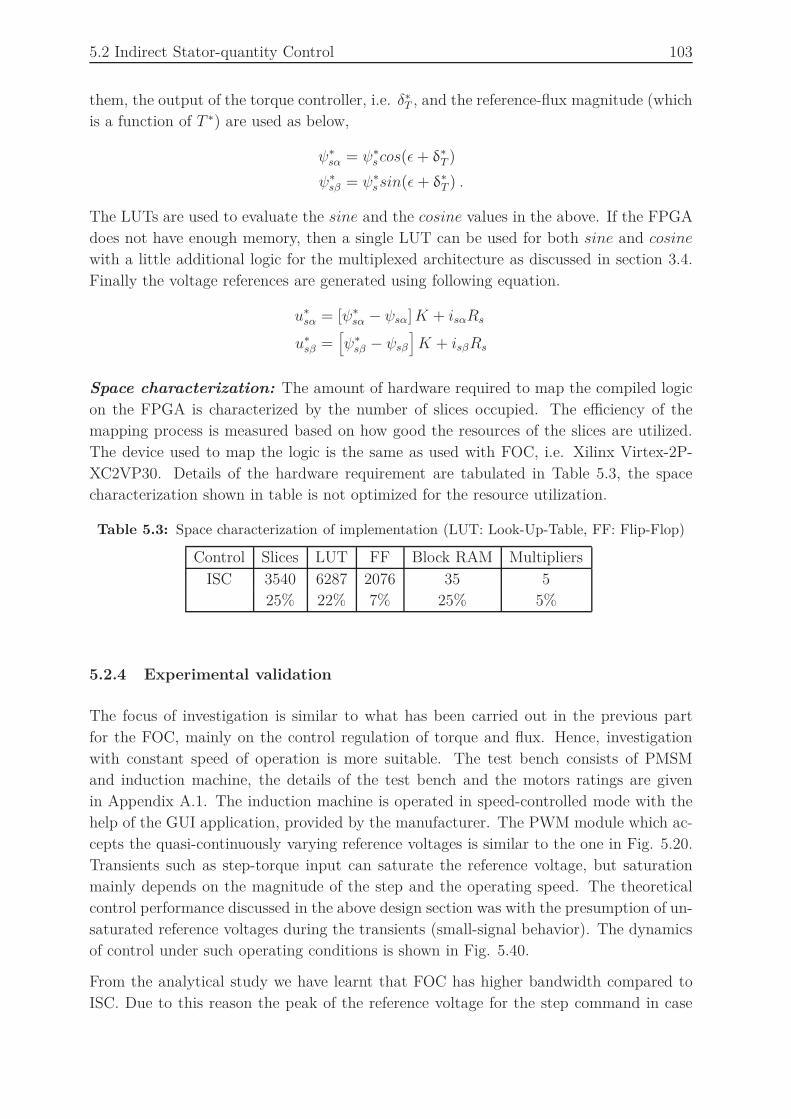
5.2 Indirect Stator-quantity Control 103
them, the output of the torque controller, i.e. δ∗T , and the reference-flux magnitude (which
is a function of T ∗) are used as below,
ψ∗sα = ψ∗
scos(ǫ+ δ∗T )
ψ∗sβ = ψ∗
ssin(ǫ+ δ∗T ) .
The LUTs are used to evaluate the sine and the cosine values in the above. If the FPGA
does not have enough memory, then a single LUT can be used for both sine and cosine
with a little additional logic for the multiplexed architecture as discussed in section 3.4.
Finally the voltage references are generated using following equation.
u∗sα = [ψ∗
sα − ψsα]K + isαRs
u∗sβ =
[
ψ∗sβ − ψsβ
]
K + isβRs
Space characterization: The amount of hardware required to map the compiled logic
on the FPGA is characterized by the number of slices occupied. The efficiency of the
mapping process is measured based on how good the resources of the slices are utilized.
The device used to map the logic is the same as used with FOC, i.e. Xilinx Virtex-2P-
XC2VP30. Details of the hardware requirement are tabulated in Table 5.3, the space
characterization shown in table is not optimized for the resource utilization.
Table 5.3: Space characterization of implementation (LUT: Look-Up-Table, FF: Flip-Flop)
Control Slices LUT FF Block RAM Multipliers
ISC 3540 6287 2076 35 5
25% 22% 7% 25% 5%
5.2.4 Experimental validation
The focus of investigation is similar to what has been carried out in the previous part
for the FOC, mainly on the control regulation of torque and flux. Hence, investigation
with constant speed of operation is more suitable. The test bench consists of PMSM
and induction machine, the details of the test bench and the motors ratings are given
in Appendix A.1. The induction machine is operated in speed-controlled mode with the
help of the GUI application, provided by the manufacturer. The PWM module which ac-
cepts the quasi-continuously varying reference voltages is similar to the one in Fig. 5.20.
Transients such as step-torque input can saturate the reference voltage, but saturation
mainly depends on the magnitude of the step and the operating speed. The theoretical
control performance discussed in the above design section was with the presumption of un-
saturated reference voltages during the transients (small-signal behavior). The dynamics
of control under such operating conditions is shown in Fig. 5.40.
From the analytical study we have learnt that FOC has higher bandwidth compared to
ISC. Due to this reason the peak of the reference voltage for the step command in case

104 5 Design of Pulse-Width-Modulation-based Motor Control on a FPGA
0 0.2 0.4 0.6 0.8 1 1.2 1.4 1.6 1.8 2
x 10-3
-150
-100
-50
0
50
100
150
Volt
age
(V)
Time (s)
Figure 5.40: Carrier and reference voltage during 50% rated torque transient under unsatu-
rated conditions
of FOC is much higher than ISC; it is evident from the comparison of Fig. 5.40 and 5.21.
As the reference voltages for the saturated condition resemble the responses seen in FOC
(Fig. 5.22 and 5.23), it is unnecessary to repeat here.
The feedback filter for the current measurement used here remains the same as the one in
FOC (ref. Fig. 5.19). The experimental results for control dynamics and regulation can
be seen in Fig. 5.41 for a step torque input with same operating conditions as in Fig. 5.24.
In this figure, the blue-colored graph corresponds to continuous behavior of the actual
experimental setup, which shows the bandwidth as 2 kHz. The experimentally evaluated
0 0.1 0.2 0.3 0.4 0.5 0.6 0.7 0.8 0.9 1
x 10-3
0
0.5
1
1.5
2
To
rqu
e (N
m)
Reference
Actual
Ideal
0 0.1 0.2 0.3 0.4 0.5 0.6 0.7 0.8 0.9 1
x 10-3
0.09
0.092
0.094
0.096
0.098
0.1
Flu
x (
Wb
)
Time (s)
Reference
Actual
Figure 5.41: Torque and flux-magnitude response with ISC under unsaturated condition (0 pu
speed)
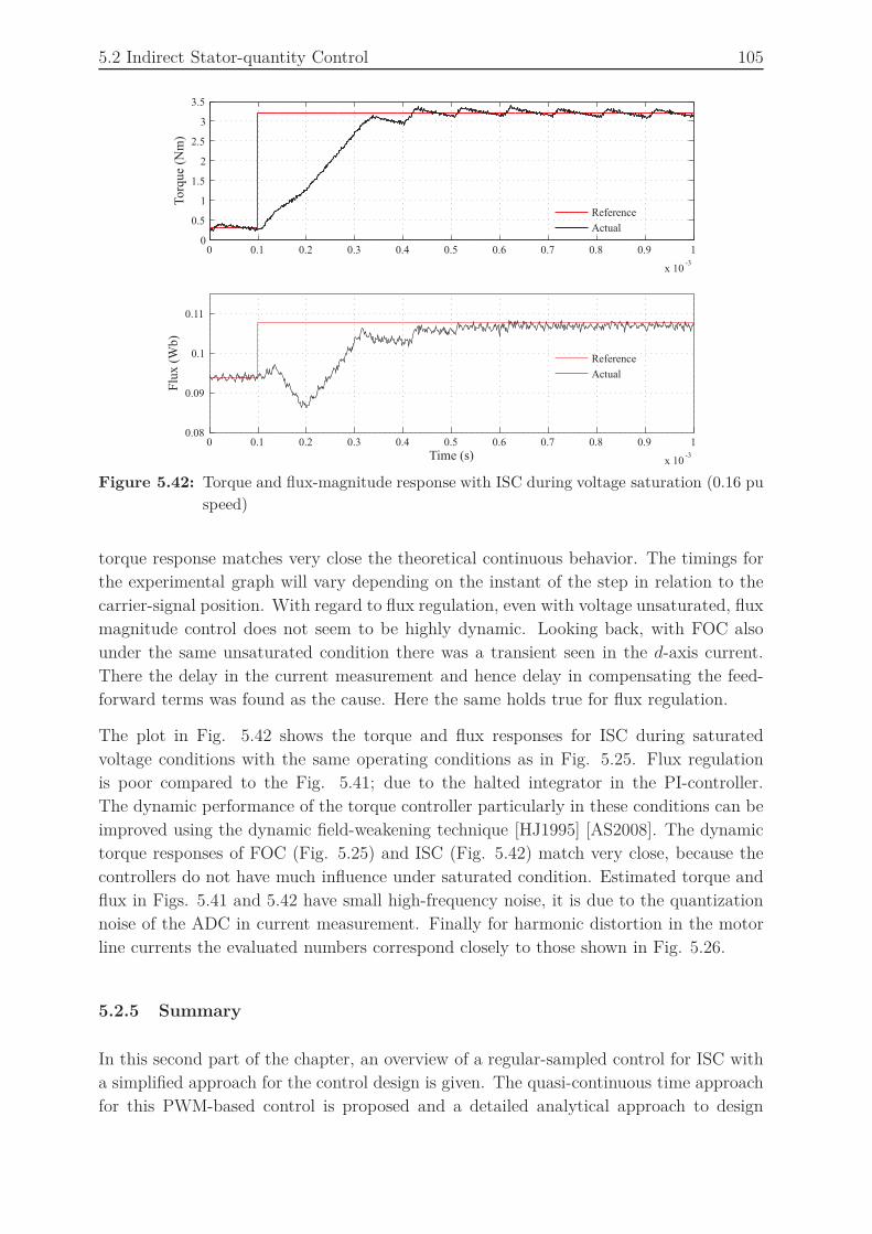
5.2 Indirect Stator-quantity Control 105
0 0.1 0.2 0.3 0.4 0.5 0.6 0.7 0.8 0.9 1
x 10-3
0
0.5
1
1.5
2
2.5
3
3.5
Torq
ue
(Nm
)
Reference
Actual
0 0.1 0.2 0.3 0.4 0.5 0.6 0.7 0.8 0.9 1
x 10-3
0.08
0.09
0.1
0.11
Flu
x (
Wb)
Time (s)
Reference
Actual
Figure 5.42: Torque and flux-magnitude response with ISC during voltage saturation (0.16 pu
speed)
torque response matches very close the theoretical continuous behavior. The timings for
the experimental graph will vary depending on the instant of the step in relation to the
carrier-signal position. With regard to flux regulation, even with voltage unsaturated, flux
magnitude control does not seem to be highly dynamic. Looking back, with FOC also
under the same unsaturated condition there was a transient seen in the d-axis current.
There the delay in the current measurement and hence delay in compensating the feed-
forward terms was found as the cause. Here the same holds true for flux regulation.
The plot in Fig. 5.42 shows the torque and flux responses for ISC during saturated
voltage conditions with the same operating conditions as in Fig. 5.25. Flux regulation
is poor compared to the Fig. 5.41; due to the halted integrator in the PI-controller.
The dynamic performance of the torque controller particularly in these conditions can be
improved using the dynamic field-weakening technique [HJ1995] [AS2008]. The dynamic
torque responses of FOC (Fig. 5.25) and ISC (Fig. 5.42) match very close, because the
controllers do not have much influence under saturated condition. Estimated torque and
flux in Figs. 5.41 and 5.42 have small high-frequency noise, it is due to the quantization
noise of the ADC in current measurement. Finally for harmonic distortion in the motor
line currents the evaluated numbers correspond closely to those shown in Fig. 5.26.
5.2.5 Summary
In this second part of the chapter, an overview of a regular-sampled control for ISC with
a simplified approach for the control design is given. The quasi-continuous time approach
for this PWM-based control is proposed and a detailed analytical approach to design

106 5 Design of Pulse-Width-Modulation-based Motor Control on a FPGA
the controller is presented. To realize it on a digital hardware, a FPGA capable of true
parallel processing has been utilized; implementation details are presented. From the
experiments it is proved that with the quasi-continuous approach the controller dynam-
ics can be improved reasonably, compared to a sampled controller without increase in
switching frequency of the inverter. Also the harmonic distortion produced by this highly
dynamic control is low and well around the best possible value. The small delay in current
measurement in the range of few microseconds is unavoidable due to practical constraints.
In the quasi-continuous approach these delays can be exploited to enhance the dynamic
performance, similar to FOC.
As mentioned in the previous section, with a feedback low-pass filter it is possible to
reduce the slope and ripple of the measured values of the motor line currents which allows
the designer to further tune the controller to achieve highest dynamics.
107
6 Design of Direct Torque Control on a FPGA
In the previous chapter a detailed study of a FPGA-based quasi-continuous PWM-based
control has been presented. In this chapter the design of hysteresis-type Direct Torque
Control (DTC) [TN1986] will be discussed. DTC is known as the best in the class for
the dynamics. However, the switching frequency of the inverter under DTC is mainly
decided by the flux- and the torque-controller output switching counts. It is known
that with fixed hysteresis bands [AH1993], the switching frequency is varying as the
operating point changes. It is possible, however, to keep the averaged switching frequency
constant by adaptation of the hysteresis bands. The switching frequency is a function of
both torque and flux bands, so that one can find different combinations of the flux and
torque bands to achieve a particular switching frequency. However, which combination
of bands is optimal for the control is a very important question. In this chapter, it is
proposed to select the hysteresis bands based on the criterion of minimum distortion
in the motor currents for the required switching frequency. An analytical procedure
is presented to calculate these optimal bands for the permanent-magnet synchronous
motor. These analytical results are first cross-verified with simulation studies and finally
validated by detailed experimentation. In order not to degrade the hysteresis control
performance by computational delay, a FPGA-based control platform is used for realizing
a quasi-continuous DTC. Due to the quasi-continuous approach for the implementation,
the analytical investigations are expected to become simpler and clearer.
6.1 Introduction
DTC for AC motor drives is known in drives industry for more than two decades. Another
control similar to DTC is the Direct Self Control (DSC) [DE1988]. Both inventions have
been published around the same time in the middle 1980s. These controls are known for
their highest control dynamics of torque regulation and both of them utilize hysteresis
controllers to regulate the torque and flux of the motor. The main difference exists in the
trajectory of the flux control: DSC guides the flux vector along a hexagonal trajectory (or
18-corner), while with DTC it is circular. The application of DSC is seen mainly in high-
power traction drives [AS2004], because it can cope with rather low switching frequencies,
which is a characteristic of such drives. DTC is utilized with low and medium power drives
due to its better THD and as higher switching frequency are available [ABB-01] [ABB-02].
Our discussion in this chapter is limited only to DTC.
The standard DTC is very simple to implement. The control performance does not de-
pend much on parameter variations, compared to the cascaded current control or FOC.

108 6 Design of Direct Torque Control on a FPGA
DTC, however, has the inherent problem of a varying switching frequency with constant
hysteresis bands, which is undesired for some applications. In order to improve this,
researchers have worked on different approaches. Contributions [UB1989] and [HP1992]
presented a similar control structure, which had the similar concept for torque-control as
in [TN1986] [DE1988], but combined with space-vector modulation (SVM). That indeed
ensures the constant switching frequency, however the inherent robustness and the dy-
namics of original DTC or DSC is being lost with this approach. Extensive research has
been seen in this direction, a detailed survey can be found in [BK2004]. In [NT1997] and
[KK1995] some additional modifications of the basic DTC are proposed to improve the
switching frequency performance. Very few publications worked on detailed analytical
approaches to analyze DTC: In [CG1994] an evaluation of the switching frequency as a
function of the hysteresis bands is given with a focus on the reduction of iron losses due to
the higher flux ripple. A similar analysis is also presented in [KS2001], where analytical
calculations of the flux- and the torque-controller switching are performed to evaluate the
switching frequency. Both publications [CG1994] and [KS2001] address that the switch-
ing frequency is not linearly related to the THD, and suggested that the flux-controller
band has to be kept reasonably narrow in comparison with the torque-controller band.
Similarly a prediction technique is employed to improve the conventional DTC’s torque-
and flux-ripple performance in [GP2009] [BV2010]. In spite of many such developments
in DTC, still it has not been able to make a significant impact in capturing the market of
standard and servo drives. In fact, this is still dominated by PWM controls; the reasons
lie in their lower total harmonic distortion (THD) and the constant switching frequency
of the inverter.
None of the publications from the literature survey has proposed a strategy how to select
the hysteresis bands in order to keep the switching frequency constant and/or to aim
for optimal THD design. In this chapter, the main focus is to present a completely
analytical and off-line approach to evaluate the optimal hysteresis bands, which ensure
constant switching frequency for the whole operating region of the drive. The criterion
for the selection of the hysteresis bands is based on the minimum distortion or THD1
in the motor currents. In the course of the proposed method’s evaluation procedure,
comparisons with simulation results are given at every step. After the off-line evaluation
of the optimal hysteresis bands, experiments are carried out for the validation.
It is well known that the performance of the hysteresis controllers depends very much on
the computational delay or dead-time of the control. In order to ensure the control real-
ization behaving very close to continuous-time performance, a FPGA is used for control
implementations. As the analysis of continuous-time systems is much simpler, compared
to sampled systems, this circumstance also provides a greater flexibility for the control
behavior analysis.
This chapter is organized as follows: In section 6.2, an analytical evaluation of the torque-
and flux-controller output frequencies, the inverter switching frequency and the THD of
1Though the current is not exactly ‘harmonic’, we use further the introduced term ‘THD’.

6.2 Analytical analysis of DTC 109
motor currents as a function of speed and load is given. These analytical findings are
compared with simulation results at every step. The criterion for selecting the optimal
hysteresis bands depending on the operating point of the motor is also presented in the
same section. Details of implementation on the FPGA platform for the proposed control
structure are presented in section 6.3. Experimental results are given in section 6.4,
containing a detailed comparison with analytical findings and a comparative performance
study in terms of dynamics and current distortion with PWM-based controls, which have
been discussed in chapter 5. This chapter closes with section 6.5 in which some final
conclusions are drawn.
6.2 Analytical analysis of DTC
6.2.1 Basics of DTC
Henceforth wherever DTC is mentioned, it is always referred to the original conventional
hysteresis type [TN1986]. The common realization of DTC is on a sequentially executing
digital signal processor (DSP). However, such a realization will incorporate computational
delays and hence a dead-time in the control loop, which is typically in the range of 25–
50 µs. With such control realization, DTC performance cannot be predicted accurately.
To analyze the potential maximum performance of DTC, it is necessary to assume a
continuous-time realization, which can be a close approximation in a quasi-continuous
way with very small sampling times. The basic block diagram representation of DTC is
shown in Fig. 6.1. For the discussion in this chapter we have chosen a permanent-magnet
synchronous motor (PMSM) with surface-mounted magnets. The corresponding motor
parameters can be found in Appendix A.1.
The fundamental idea of torque-control in DTC is controlling the angle between the
stator- and the rotor-flux vectors, which is also known as the torque angle δT . To do
this, there is no need of position information of the rotor flux or the exact position of
the stator flux. It is only required to know in which sector of the hexagon (as marked
in Fig. 6.2) the stator-flux vector is. With this information, to increase the torque the
flux-vector is accelerated from the present position in the direction of rotation with the
help of appropriate active voltage vectors (v1..v6). E.g. in sector 1, voltage vector v2 and
v3 are used (see Fig. 6.2); v2 increases both the flux magnitude and the torque, while
v3 increases the torque, but reduces the flux magnitude. Similarly, for sector 2 vectors
(v3,v4), sector 3 (v4,v5), sector 4 (v5,v6), sector 5 (v6,v1), and sector 6 (v1,v2) are used.
The torque produced increases with the sine of the angle between stator-flux and rotor-
flux vector, see (5.10). At lower speeds, the stator-flux vector can be moved away from
the rotor-flux vector very quickly, which implies faster torque increase. This behavior
slows down with speed increase, because the rotor-flux vector is following up with higher
speed.
110 6 Design of Direct Torque Control on a FPGA
LU
T-
-f(T )
*
T ∗
Tψ∗
s
ψs
Sψ
ST
MotorObserver
Sector
3
Figure 6.1: Block diagram of DTC
Secto
r 1
Sector 2Sector 3
Sec
tor
4
Sector5 Sector6
v6 (101)
α
β
θs
v3 (010) v 2
(110
)
v1(100)
v4(011)
v 5(0
01)
d
q
x
y
v0,v7
LsisqδT
ψp
ψ s(t)
ψ s(t)
Synchronously rotating coordinatesStator-fixed coordinates
Figure 6.2: Stator-flux trajectory within the flux band in stator-fixed coordinates and in syn-
chronously rotating coordinates
The torque produced in a PMSM is a result of the interaction between the rotor flux, i.e.
the permanent flux of the magnets, and the stator current. Hence, the stator flux consists
of the linkage with the rotor flux and the part contributed by the stator current via the
stator-armature inductance. Therefore, unlike in the case of induction machines with
FOC, in PMSM the flux magnitude reference is a function of the torque reference, as it is
depicted in Fig. 6.1 (which was also seen in case of ISC). In order to regulate the torque
in either direction, the torque controller usually includes a three-level hysteresis. For the
flux-controller it is adequate to employ a simple two-level hysteresis, because it regulates
only the magnitude. The outputs of torque and flux controllers and the sector of flux
location are the inputs to the look-up table (LUT), to select appropriate voltage vectors
as mentioned above. In order to keep the switching frequency low, active vectors are only
used to increase the torque, while for reducing the torque the zero-voltage vector v0 or v7
is applied in case of positive speed. In case of negative speed, the strategy is opposite.

6.2 Analytical analysis of DTC 111
Virtually, angle (θs) and magnitude (ψs) of the stator flux remain unchanged while the
zero-voltage vector is applied; this is due to the small resistive voltage drop. Hence the
flux-controller output is expected to remain unchanged during this period. Depending on
the inputs from the controllers and the stator-flux location, the look-up table (LUT) will
choose the switching signals for the inverter. From the basic understanding of hysteresis
controllers, it is evident here that the switching signal will not change periodically like in
the case of PWM controls. Hence, one can define the switching frequency as the number
of pulses (two switch change-overs in opposite directions count as one pulse) within a
time interval. The time interval should be long enough for better averaging. Following
notations are used for the different frequencies of the control:
Fψ: Frequency of flux-controller output
FT : Frequency of torque-controller output
Fs: Switching frequency of inverter (averaged number of changes of switch Sa, Sb and
Sc, respectively)
The switching frequency of the inverter can be approximated via the torque- and the
flux-controller output frequency as,
Fs ≈Fψ + FT
3(6.1)
because the switching commands are distributed among the three phases. From the above
(6.1) it is evident that the inverter switching frequency Fs can be controlled by varying
Fψ or FT or both together. Hence it is essential to do a detailed theoretical analysis
how these individual frequencies Fψ, FT vary with the operating point of the motor.
The steady-state operating condition of the motor should be considered for the analysis,
because transients are short and of little importance in the context.
6.2.2 Detailed insight of DTC
The analysis of torque- and flux-controller output frequencies is done with the following
assumptions:
• Steady-state operating condition: The load disturbances are neglected, the speed is
considered as constant and positive (anticlockwise rotation of vectors)
• DC-link voltage of the inverter is constant
• Motor is operating in constant-torque region
• Control is realized in continuous-time fashion.
The behavior of the flux trajectory in any sector resembles that of the other sectors.
This is because in any sector different combinations of two active vectors are used, both
increase the torque, but always the leading vector of the nominated pair reduces the flux
magnitude, while the trailing vector increases the magnitude. Therefore, if the analysis is
112 6 Design of Direct Torque Control on a FPGA
carried out for only one sector, it is possible to extend it to the complete cycle of rotation.
Hence, only sector 1 is considered in the following analysis.
To make the analysis easier, it is preferred to use different coordinate systems. The rotor-
flux d/q coordinate system is used to analyze the torque controller and the stator-flux
aligned x/y coordinates for the flux controller.
6.2.2.1 Evaluation of torque-controller frequency FT
The stator-voltage equations in d/q components can be written as
usd = Rsisd − ωLsisq + Ls isd
usq = Rsisq + ω(Lsisd + ψp) + Lsisq(6.2)
where Rs, Ls, ψp and ω are the stator resistance, inductance, rotor permanent-flux linkage
and the speed, respectively. The electromagnetic torque for the considered PMSM can be
given as
T =3
2pψpisq ∝ isq (6.3)
where p is the number of pole pairs. From (6.3), torque can be independently controlled
by controlling the current in the q-axis, and hence the small increase or decrease of torque
within the hysteresis band of ∆T can be written as,
∆T =3
2pψp∆isq . (6.4)
The time taken to produce a change ∆isq in the q-axis current can be written as in (6.5),
using (6.2). In (6.5), with the assumption of the constant-torque region of operation (and
a surface-mounted PMSM), the mean value of isd is zero and the effect of its instantaneous
value as voltage drop ωLsisd is very small and hence neglected:
∆t =Ls∆isq
uq − ωψp − Rsisq(6.5)
where uq is the applied voltage vector in the q-axis. The value of time taken by the
controller to increase the torque from the lower to the upper hysteresis threshold shall
now be defined as t23 and the time to decrease it back to lower threshold is t0 (depicted in
Fig. 6.3). During the rising slope in interval t23, the driving voltage uq is the q-component
of the vectors v2 and v3, respectively. For an averaging calculation, u23q is resulting from
a weighted mean value of v2q and v3q according to their duty ratios α2 = t2t23
and α3 = t3t23
,
respectively,
u23q = α2v2q + α3v3q = u2q + u3q (6.6)
where v2q and v3q are the q-axis voltage contributed by the vectors v2 and v3, respectively.
Note that α2 + α3 = 1.
6.2 Analytical analysis of DTC 113
During the falling slope, the zero-voltage vector is applied, so that uq is zero in the interval
t0. Consequently the timings can be evaluated as follows:
t23 = ∆isq
[
Lsu23q − ωψp −Rsisq
]
t0 = ∆isq
[
Ls0 − ωψp − Rsisq
] (6.7)
Time behavior depicted in Fig. 6.3, holds that the flux-controller output frequency is
higher than that of the torque control, the calculation of t23 does not depend on such
an assumption. In a different situation, when during a complete rising torque ramp only
either v2 or v3 are applied, t23 can be understood as the statistical mean value for the
whole cycle.
In order to calculate these timings it is necessary to evaluate u23q(θs). At first, the
components v2q, v3q shall be determined. From Fig. 6.2, it can be seen that the angle
of the q-axis measured from the stator-fixed α-axis is [θs − δT + 90
]. With some basic
coordinate transformation that results in
v2q(θs − δT ) = udc2
3cos(θs − δT + 30
)
v3q(θs − δT ) = udc2
3cos(θs − δT − 30
).(6.8)
So we can learn that these components depend on the angle [θs − δT ]. The resulting
curves are shown in Fig. 6.4. It is visible that at the start of sector 1, which is the
marked interval from –30
to +30
(in no-load case), v2q has the highest magnitude which
is 2udc3
, and this will keep reducing according to a cosine function, as the flux vector
travels in the sector and becomes the smallest at the end of the sector, equal to udc3
. The
other vector v3q also produces a similar voltage but with opposite behavior. This clarifies,
the closer to the start and to the end of the sector, one of these active vectors yields the
highest magnitude of the voltage and hence the highest slope for increasing the torque,
∆T ∆T
∆ψs∆ψs
t23t0
t2
t3
v2v2
v3v3
t
t
Figure 6.3: Flux and torque change within the band

114 6 Design of Direct Torque Control on a FPGA
while the other vector is at its minimum. The smallest voltage produced by these vectors,
either at the start or at the end of the sector can be smaller in magnitude compared to
the back-EMF (specifically when the motor is operating close to rated speed), and will
thus produce a reducing instead of an increasing torque slope. This is due to the fact that
at the particular point the applied q-axis voltage is less than the back-EMF ωψp .
For motoring operation, the dotted box of the sector 1 in Fig. 6.4 will be shifted to the
left by the load angle δT , the curves themselves remain unchanged in the representation
versus [θs − δT ]. For generating operation, the box will be shifted towards the right.
The second step is to determine the ratios α2, α3 in (6.6), which can be done using the
space-vector-modulation (SVM) calculus. The required fictitious reference stator-voltage
vector for the SVM is calculated based on the assumption of the stator-flux vector having
a constant magnitude and rotating with constant velocity. The only difference is that
α2, α3 are not the duty ratios with respect to the full pulse period of SVM, but with
respect to the time of active voltage vectors t23. That means these values depend only
on the angle or the position of this fictitious voltage vector, not on the magnitude. If
the ohmic voltage drop is neglected, the voltage vector direction can be assumed to be
orthogonal to the flux vector so that the result shown in Fig. 6.5 depends only on the
flux angle θs and not on the load condition. With that insight we may rewrite (6.6) with
the functional arguments as
u23q(θs, δT ) = α2(θs)v2q(θs − δT ) + α3(θs)v3q(θs − δT )
= u2q(θs, δT ) + u3q(θs, δT ) .(6.9)
The effective q-axis voltage u23q and the individual contributions of active vectors u2q,u3q
are shown in Fig. 6.6 for the no-load and the rated-load case. As it can be seen, the
available q-axis voltage is reduced with the increasing load torque. Using these evaluated
-60 -40 -20 0 20 40 600
0.1
0.2
0.3
0.4
0.5
0.6
0.7
0.8
0.9
1
θs- δ
T(degree)
No
rmal
ized
vo
ltag
e
v2q
v3q
Figure 6.4: Voltage components v2q and v3q versus θs − δT . (Reference value of normalization
is 2udc3 )

6.2 Analytical analysis of DTC 115
-30 -20 -10 0 10 20 300
0.1
0.2
0.3
0.4
0.5
0.6
0.7
0.8
0.9
1
θs (degree)
Duty
rat
io
α2
α3
Figure 6.5: Duty ratios α2, α3 vs. θs in sector 1
-30 -20 -10 0 10 20 300
0.1
0.2
0.3
0.4
0.5
0.6
0.7
0.8
0.9
1
No
rmal
ized
vo
ltag
e
θs (degree)
u3q
u23q
u2q
Figure 6.6: u23q produced by active vectors (solid line: at no-load, dashed line: at rated load)
voltages, the torque-controller switching frequency FT can be calculated as an average
over sector 1.
FT =1
TSector1
∫
Sector1
(1
t23 + t0
)
dt
=1
π/3
∫ −π/6
−π/6
(1
t23 + t0
)
dθs
(6.10)
The equations (6.5)–(6.10) which are used to evaluate FT reveal that it depends only on
ω, ∆T and the load, but is independent of the flux-controller band ∆ψs.
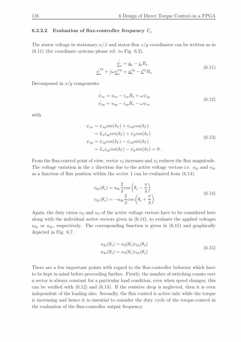
116 6 Design of Direct Torque Control on a FPGA
6.2.2.2 Evaluation of flux-controller frequency Fψ
The stator voltage in stationary α/β and stator-flux x/y coordinates can be written as in
(6.11) (for coordinate systems please ref. to Fig. 6.2).
ψs
= us − isRs
ψxy
s+ jωψxy
s= uxys − ixys Rs
(6.11)
Decomposed in x/y components:
ψsx = usx − isxRs + ωψsy
ψsy = usy − isyRs − ωψsx(6.12)
with
ψsx = ψsqsin(δT ) + ψsdcos(δT )
= Lsisqsin(δT ) + ψpcos(δT )
ψsy = ψsqcos(δT ) − ψsdsin(δT )
= Lsisqcos(δT ) − ψpsin(δT ) = 0 .
(6.13)
From the flux-control point of view, vector v2 increases and v3 reduces the flux magnitude.
The voltage variation in the x direction due to the active voltage vectors i.e. v2x and v3x
as a function of flux position within the sector 1 can be evaluated from (6.14).
v2x(θs) = udc2
3cos
(
θs −π
3
)
v3x(θs) = −udc2
3cos
(
θs +π
3
) (6.14)
Again, the duty ratios α2 and α3 of the active voltage vectors have to be considered here
along with the individual active vectors given in (6.14), to evaluate the applied voltages
u2x or u3x, respectively. The corresponding function is given in (6.15) and graphically
depicted in Fig. 6.7.
u2x(θs) = α2(θs)v2x(θs)
u3x(θs) = α3(θs)v3x(θs)(6.15)
There are a few important points with regard to the flux-controller behavior which have
to be kept in mind before proceeding further. Firstly, the number of switching counts over
a sector is always constant for a particular load condition, even when speed changes; this
can be verified with (6.12) and (6.13). If the resistive drop is neglected, then it is even
independent of the loading also. Secondly, the flux control is active only while the torque
is increasing and hence it is essential to consider the duty cycle of the torque-control in
the evaluation of the flux-controller output frequency.

6.2 Analytical analysis of DTC 117
u2x
-30 -20 -10 0 10 20 30-0.25
-0.2
-0.15
-0.1
-0.05
0
0.05
0.1
0.15
0.2
0.25
no
rmal
ized
vo
ltag
e
θs (degree)
u3x
Figure 6.7: u2x u3x produced by active vectors as function of θs
The time intervals taken to increase and decrease the flux magnitude within the band
∆ψs are t2 and t3, given as a function of θs in (6.16) using (6.12) and (6.13).
t2(θs) =
[
∆ψsu2x(θs) − Rsisqsin(δT )
]
t3(θs) =
[
−∆ψsu3x(θs) − Rsisqsin(δT )
] (6.16)
The evaluation of the flux frequency is easier, compared to the torque-controller frequency,
because the two vector components u2x and u3x can be regarded separately with respect
to controlling the flux magnitude. Moreover, provided that the ohmic voltage drop is
neglected, the two vector components are equal in magnitude with opposite sign. Hence
the switching counts can be directly calculated from only one voltage vector. Therefore,
the magnitude of the flux which can be produced by one of the active vectors in the whole
sector is calculated and then divided by the flux band, to evaluate the switching counts.
Then the frequency is evaluated by finding out the ratio of the counts and the time taken,
which is a function of the operating speed ω. The total amount of flux magnitude can be
increased by the voltage u2x in sector 1 according to (6.17).
ψs:1 =1
ω
∫ π6
−π6
[u2x(θs)TM − isxRs] dθs (6.17)
where TM is the duty cycle of the torque-controller output, defined as TM = t23
t23+t0(inde-
pendent of ∆T ), graphically shown in Fig. 6.8 as a function of normalized speed. Using the
flux magnitude from (6.17), the number of switching counts Ns:1 and the flux-controller
output frequency can be evaluated as,
Ns:1 =ψs:1∆ψs
Fψs =Ns:1π
3ω
.(6.18)

118 6 Design of Direct Torque Control on a FPGA
0.1 0.2 0.3 0.4 0.5 0.6 0.7 0.8 0.9 1 1.10
0.1
0.2
0.3
0.4
0.5
0.6
TM
Normalized ω
Figure 6.8: Torque-controller duty cycle as a function of normalized motor speed (Rated speed
of the motor is used as reference quantity for normalization)
Analogous to the case of FT , the evaluated Fψs using (6.14)–(6.18) confirms that it is
independent of the torque band ∆T .
Using the above analytical consideration, the torque- and the flux-controller frequency can
be computed for different operating conditions; i.e. at different speeds and load torques.
In order to validate them, a detailed simulation study is carried out in Matlab-Simulink
for different operating speeds. The results are then interpolated for the whole operating
0.2 0.3 0.4 0.5 0.6 0.7 0.8 0.9 1 1.1 1.2
0.5
1
1.5
2
2.5x 10
4
∆T=5%
∆T=7%
∆T=10%
∆T=15%
∆T=20%
0.2 0.3 0.4 0.5 0.6 0.7 0.8 0.9 1 1.1 1.2
0.5
1
1.5
2
2.5
3
3.5
4
4.5x 10
4
Normalized ω
∆ψ =1%
∆ψ =1.33%
∆ψ =1.66%
∆ψ =2%
∆ψ =2.33%
F(H
z)ψ
FT
(Hz)
Figure 6.9: Comparison of output frequency variation for the torque- and the flux-controller
of the motor given in Appendix A.1 (analytical (+) and simulation (-) results)
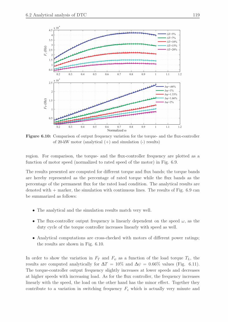
6.2 Analytical analysis of DTC 119
0.2 0.3 0.4 0.5 0.6 0.7 0.8 0.9 1 1.1 1.2
0.5
1
1.5
2
2.5
3
3.5
4
4.5x 10
4
∆T=5%
∆T=7%
∆T=10%
∆T=15%
∆T=20%
0.2 0.3 0.4 0.5 0.6 0.7 0.8 0.9 1 1.1 1.2
0.5
1
1.5
2
2.5x 10
4
Normalized ω
∆ψ=.66%
∆ψ=1%
∆ψ=1.33%
∆ψ=1.66%
∆ψ=2%
F(H
z)ψ
FT
(Hz)
Figure 6.10: Comparison of output frequency variation for the torque- and the flux-controller
of 20-kW motor (analytical (+) and simulation (-) results)
region. For comparison, the torque- and the flux-controller frequency are plotted as a
function of motor speed (normalized to rated speed of the motor) in Fig. 6.9.
The results presented are computed for different torque and flux bands; the torque bands
are hereby represented as the percentage of rated torque while the flux bands as the
percentage of the permanent flux for the rated load condition. The analytical results are
denoted with + marker, the simulation with continuous lines. The results of Fig. 6.9 can
be summarized as follows:
• The analytical and the simulation results match very well.
• The flux-controller output frequency is linearly dependent on the speed ω, as the
duty cycle of the torque controller increases linearly with speed as well.
• Analytical computations are cross-checked with motors of different power ratings;
the results are shown in Fig. 6.10.
In order to show the variation in FT and Fψ as a function of the load torque TL, the
results are computed analytically for ∆T = 10% and ∆ψ = 0.66% values (Fig. 6.11).
The torque-controller output frequency slightly increases at lower speeds and decreases
at higher speeds with increasing load. As for the flux controller, the frequency increases
linearly with the speed, the load on the other hand has the minor effect. Together they
contribute to a variation in switching frequency Fs which is actually very minute and
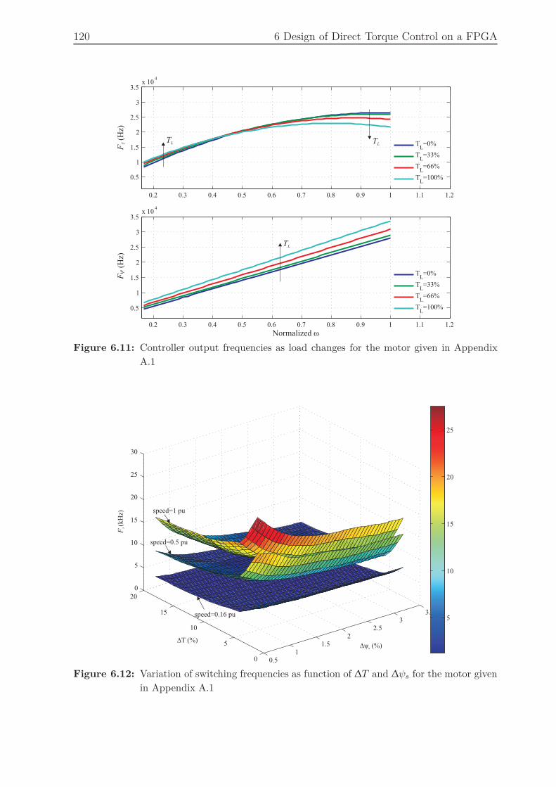
120 6 Design of Direct Torque Control on a FPGA
0.2 0.3 0.4 0.5 0.6 0.7 0.8 0.9 1 1.1 1.2
0.5
1
1.5
2
2.5
3
3.5x 10
4
TL=0%
TL=33%
TL=66%
TL=100%
0.2 0.3 0.4 0.5 0.6 0.7 0.8 0.9 1 1.1 1.2
0.5
1
1.5
2
2.5
3
3.5x 10
4
Normalized ω
TL=0%
TL=33%
TL=66%
TL=100%
F(H
z)ψ
FT
(Hz)
TL
TL
TL
Figure 6.11: Controller output frequencies as load changes for the motor given in Appendix
A.1
0.5
1
1.5
2
2.53
3.5
0
5
10
15
20
0
5
10
15
20
25
30
∆ψs (%)∆T (%)
Fs(k
Hz)
5
10
15
20
25
speed=1 pu
speed=0.5 pu
speed=0.16 pu
Figure 6.12: Variation of switching frequencies as function of ∆T and ∆ψs for the motor given
in Appendix A.1
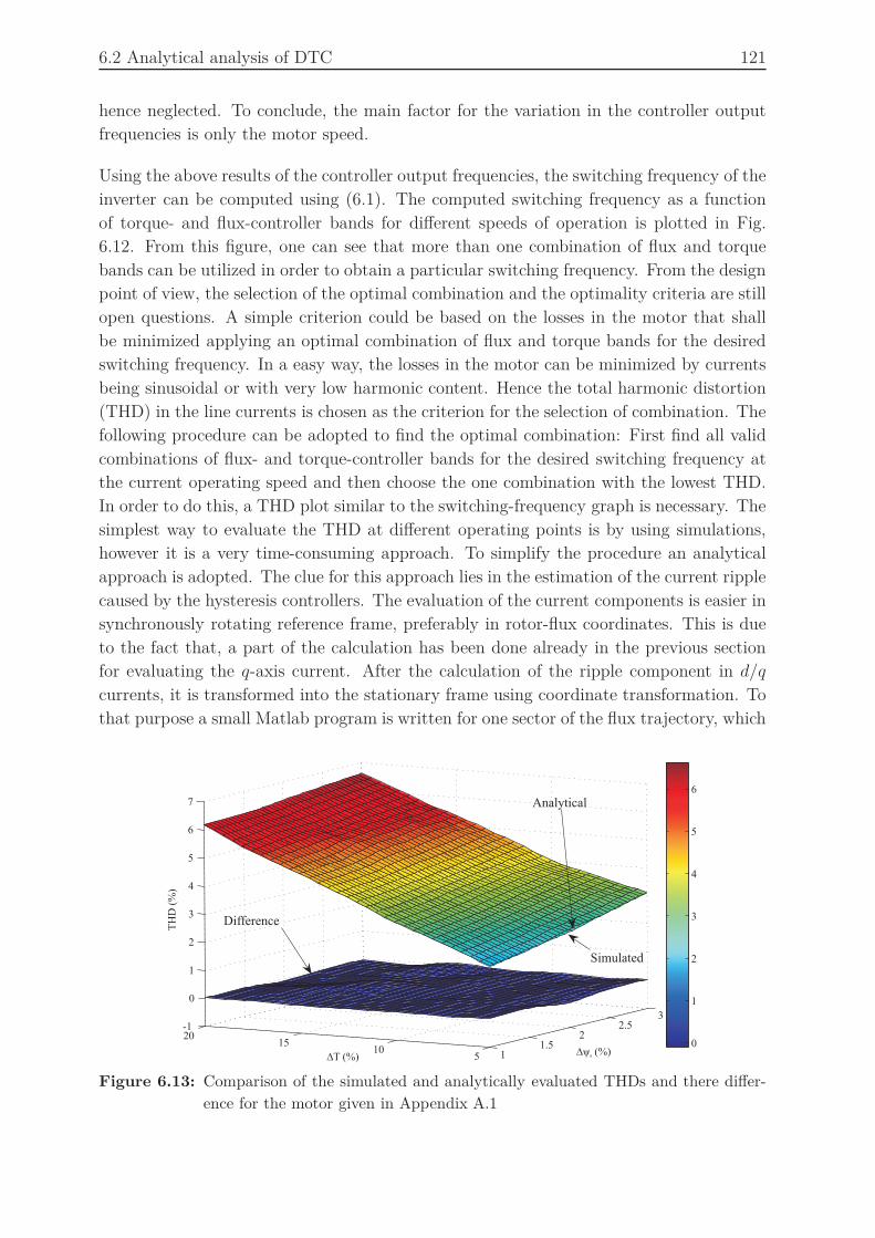
6.2 Analytical analysis of DTC 121
hence neglected. To conclude, the main factor for the variation in the controller output
frequencies is only the motor speed.
Using the above results of the controller output frequencies, the switching frequency of the
inverter can be computed using (6.1). The computed switching frequency as a function
of torque- and flux-controller bands for different speeds of operation is plotted in Fig.
6.12. From this figure, one can see that more than one combination of flux and torque
bands can be utilized in order to obtain a particular switching frequency. From the design
point of view, the selection of the optimal combination and the optimality criteria are still
open questions. A simple criterion could be based on the losses in the motor that shall
be minimized applying an optimal combination of flux and torque bands for the desired
switching frequency. In a easy way, the losses in the motor can be minimized by currents
being sinusoidal or with very low harmonic content. Hence the total harmonic distortion
(THD) in the line currents is chosen as the criterion for the selection of combination. The
following procedure can be adopted to find the optimal combination: First find all valid
combinations of flux- and torque-controller bands for the desired switching frequency at
the current operating speed and then choose the one combination with the lowest THD.
In order to do this, a THD plot similar to the switching-frequency graph is necessary. The
simplest way to evaluate the THD at different operating points is by using simulations,
however it is a very time-consuming approach. To simplify the procedure an analytical
approach is adopted. The clue for this approach lies in the estimation of the current ripple
caused by the hysteresis controllers. The evaluation of the current components is easier in
synchronously rotating reference frame, preferably in rotor-flux coordinates. This is due
to the fact that, a part of the calculation has been done already in the previous section
for evaluating the q-axis current. After the calculation of the ripple component in d/q
currents, it is transformed into the stationary frame using coordinate transformation. To
that purpose a small Matlab program is written for one sector of the flux trajectory, which
11.5
22.5
3
510
1520-1
0
1
2
3
4
5
6
7
TH
D (
%)
0
1
2
3
4
5
6
Analytical
Difference
Simulated
∆ψs (%)∆T (%)
Figure 6.13: Comparison of the simulated and analytically evaluated THDs and there differ-
ence for the motor given in Appendix A.1

122 6 Design of Direct Torque Control on a FPGA
is recalled for the other remaining sectors. A flowchart of the program can be found in the
Appendix A.2. The different steps used in the program to evaluate the THD are briefly
explained below.
1. Initialization:
• Inputs required are motor inductance and resistance, operating speed, hystere-
sis bands, load condition
• Arbitrary values of actual flux and torque within the hysteresis bands have to
be taken
• The output of the controllers can be chosen arbitrarily
• Initial flux position at θs = −30
(start of any sector).
2. Controller: Simple relay logic can be used to incorporate the hysteresis controller.
3. Estimation: Depending on the controller output, one of the active voltage vectors
is used, and correspondingly the d- and q-axis voltages are evaluated to find the
corresponding current variation. The details of the equations involved in calculating
these currents can be found in Appendix A.2. The required estimate of torque is
calculated using (6.3), and the flux using (6.19).
ψs =√
(ψp + Lsisd)2 + (Lsisq)
2 (6.19)
4. Transition to next sector and initialization: The loop for one sector ends depending
on the number of iterations, the iteration sample time and the motor operating
speed. Once the sector is ended, the present values of flux, torque and controllers
output are carried over for the initialization of the new sector.
5. THD calculation: The evaluated d- and q-axis ripple components added to the q-
axis current corresponding to the load condition. With the help of the coordinate
transformation the current in stationary coordinates is evaluated and a Fourier
transform is applied to find the frequency components and the THD.
The program is capable of calculating automatically the THD for different combinations
of torque- and flux-hysteresis bands. The analytically evaluated THD results match very
well the results which are evaluated by simulations. A comparison of THD evaluated by
simulation and computed from the program is provided in Fig. 6.13. The error is also
shown in the same figure; it shows that the error is very small and negligible which proves
the accuracy of the proposed analytical method.
Based on the above discussed strategy, the procedure for the selection of optimal hysteresis
bands is as follows:
• Depending on the desired switching frequency and the selected operating speed of
the motor, different combinations of hysteresis bands are identified from the look-up
table (LUT) data in Fig. 6.12.
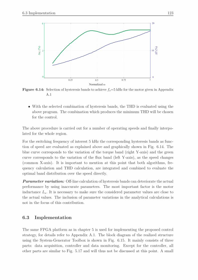
6.3 Implementation 123
Normalized ω
0
10
20
0
2
4
DT
(%)
0.5 10.750.25
∆ψ
s(%
)
Figure 6.14: Selection of hysteresis bands to achieve fs=5 kHz for the motor given in Appendix
A.1
• With the selected combination of hysteresis bands, the THD is evaluated using the
above program. The combination which produces the minimum THD will be chosen
for the control.
The above procedure is carried out for a number of operating speeds and finally interpo-
lated for the whole region.
For the switching frequency of interest 5 kHz the corresponding hysteresis bands as func-
tion of speed are evaluated as explained above and graphically shown in Fig. 6.14. The
blue curve corresponds to the variation of the torque band (right Y-axis) and the green
curve corresponds to the variation of the flux band (left Y-axis), as the speed changes
(common X-axis). It is important to mention at this point that both algorithms, fre-
quency calculation and THD calculation, are integrated and combined to evaluate the
optimal band distribution over the speed directly.
Parameter variation: Off-line calculation of hysteresis bands can deteriorate the actual
performance by using inaccurate parameters. The most important factor is the motor
inductance Ls. It is necessary to make sure the considered parameter values are close to
the actual values. The inclusion of parameter variations in the analytical calculations is
not in the focus of this contribution.
6.3 Implementation
The same FPGA platform as in chapter 5 is used for implementing the proposed control
strategy, for details refer to Appendix A.1. The block diagram of the realized structure
using the System-Generator Toolbox is shown in Fig. 6.15. It mainly consists of three
parts: data acquisition, controller and data monitoring. Except for the controller, all
other parts are similar to Fig. 5.17 and will thus not be discussed at this point. A small
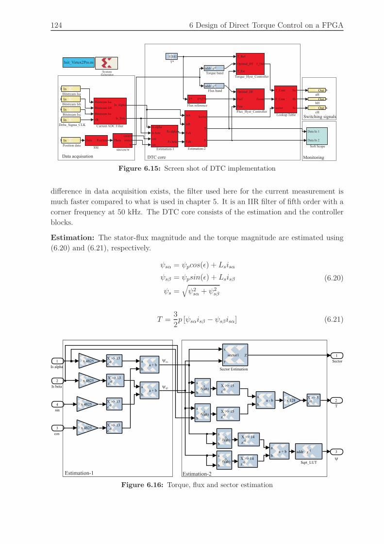
124 6 Design of Direct Torque Control on a FPGA
Data acquisation DTC core Monitoring
Switching signals
Theta
cos(e)
sin(e)
w
sin/cos/w
OutcH
OutbH
OutaH
T_Ref
Optimal_DT
T_Est
T_Out
Torque_Hyst_Controller
addr z-1
Torque band
11141
T*
Data In 1
Data In 2
Soft Scope
Data Position
SSI
In
Position data
T_Cont
F_Cont
sector
Sa
Sb
Sc
Lookup Table
Init_Virtex2Pro.m
Optimal_DF
Fref
Fest
Fcont
Flux_Hyst_Controller
T* F*(T*)
Flux reference
addr z-1
Flux band
IsA
IsB
FsA
FsB
Sector
T
F
Estimation-2
Is alpha
Is beta
cos
sin
Fs alpha
Fs beta
Estimation-1
In
Delta_Sigma_CLK
Bitstream Isa
Bitstream Isb
Bitstream Isc
clk
Is_Alpha
Is_Beta
Current ADC Filter
In
Bitstream Isc
In
Bitstream Isb
In
Bitstream Isa
SystemGenerator
Figure 6.15: Screen shot of DTC implementation
difference in data acquisition exists, the filter used here for the current measurement is
much faster compared to what is used in chapter 5. It is an IIR filter of fifth order with a
corner frequency at 50 kHz. The DTC core consists of the estimation and the controller
blocks.
Estimation: The stator-flux magnitude and the torque magnitude are estimated using
(6.20) and (6.21), respectively.
ψsα = ψpcos(ǫ) + Lsisα
ψsβ = ψpsin(ǫ) + Lsisβ
ψs =√
ψ2sα + ψ2
sβ
(6.20)
T =3
2p [ψsαisβ − ψsβisα] (6.21)
3
2
T
1
Sector
addr z-1
Sqrt_LUT
X >> 5
z-0
X >> 13
z-0
X >> 13
z-0
X >> 13
z-0
X >> 14
z-0
X >> 14
z-0
X >> 15
z-0
X >> 15
z-0
X >> 13
z-0
x
y
Zsector1
Sector Estimation
a
ba + b
a
ba - b
a
ba + b
x 128
a
b(ab)z-3
a
b(ab)z-3
a
b(ab)z-3
a
b(ab)z-3
x 4825
x 4825
x 4825
x 4825
a
ba + b
4
sin
3
cos
2
Is beta
1
Is alpha
ysb
ysa
y
Estimation-1 Estimation-2
Figure 6.16: Torque, flux and sector estimation

6.3 Implementation 125
Switching table using LUT
3
Sc
2
Sb
1
Sa
x
yZTF_vector_beta
torque_flux LUT
diff
old
Optimal TD
ZTorque_Hyst_1_optimal_ TD
Torque_Hysteresis_Logic
X >> 2
z-0
X >> 1
z-0
x
yZtable_beta
Sector LUT
a
b
a=b
z-1
a
b
a=b
z-1
a
b
a=b
z-1
and
z-0
and
z-0
and
z-0
z-1
z-1 1
2
4
1
1
1
a
ba - b
a
ba - b
diff
old
Optimal Dy
ZFlux_cont_optimal_Dy
.m file Flux_Hysteresis_Logic
7
Sector
6
T
5
Optimal TD
4
T*
3y
2
y*
1
Optimal Dy
Hysteresis Controllersz(3-bit)= S S S
2 2 2a b c2 1 0
T_out
y_out
Figure 6.17: Implementation of controller and switching table
where ǫ is the rotor position in stationary coordinates. For the control, the exact position
of the stator-flux vector is not necessary, only the identification of the sector in which
it is located is required. The sector can be found with a very simple logic using only
few relational operations between the ψsα and the ψsβ components. E.g. if both compo-
nents are greater than zero or positive, the flux can either lie in sector 2 or 1. Further if
ψsβ > ψsα·tan(30
) is “true”, then the flux is located in sector 2; if “false”, it is located
in sector 1. The same logic is applied for the different possible conditions such as when
one of the components is negative and the other is positive, as well as when both com-
ponents are negative. The estimation of the stator-flux components in α/β coordinates
using (6.20) and the sector identification is included in the block “Estimation-1”, the
flux-magnitude and the torque estimation using (6.21) in the block “Estimation-2”. The
square-root function in the flux-magnitude calculation is performed with a LUT, the logic
for the sector evaluation is done in a Matlab .m file and embedded into System-Generator.
Implementation details of these two blocks are depicted in Fig. 6.16.
Controllers: The flux controller and the torque controller are realized with simple relay
logic. These blocks are also realized with Matlab “.m” files (ref. to Fig. 6.17). The
optimal hysteresis band values are provided to both controllers as inputs from the LUT,
as a function of speed (ref. to Fig. 6.15). The switching table is realized with a LUT too,
the final selection of the switching signals Sa, Sb and Sc is done with simple relational
logic (ref. to Fig. 6.17).
Space characterization: The amount of hardware required to map the compiled logic
on the FPGA is tabulated in Table 6.1. The total time taken for the execution of the
logic is around 400 ns (10 clock latencies), thus negligible. The estimation needs 200 ns
(5 latencies) and the controller 200 ns (5 latencies) for the computation. Considering
these numbers, it is obvious that the assumption of the controller as continuous-time is
reasonable. From table 6.1 it can easily be found that the space required for DTC is
much more, compared to FOC (ref. to table 5.2). In fact the major space demand is not
for the controller but for the ∆Σ filter. As mentioned above it is a fifth-order IIR-type
filter, which has been implemented using the direct approach. In consequence the space

126 6 Design of Direct Torque Control on a FPGA
required is quite high, as already discussed in section 4.3.2. For the implementation no
specific optimal approach from the space point of view has been considered. In case of
DTC it is however possible to optimize the logic utilization with the help of multiplexed
architecture, which has been discussed in section 3.4.2.
Table 6.1: Space characterization of implementation (LUT: look-up table, FF: Flip-Flop)
Slices LUT FF Block RAM Multipliers
9162 16651 2036 47 5
(66%) (60%) (7%) (7%)
6.4 Experimental validation
The experiment is carried out with the evaluated optimal hysteresis bands derived in
the previous section 6.2. The performance of the controller is evaluated in the whole
constant-torque region. Data for THD and switching frequency are evaluated at different
operating speeds and then interpolated for the complete region. The computed THD and
switching frequency results are plotted in Fig. 6.18, for comparison the expected ideal
analytical values are also shown.
A difference in the analytical and the experimental results for switching frequency and
THD is evident from Fig. 6.18. In the complete analytical analysis, the delay and the
0.2 0.3 0.4 0.5 0.6 0.7 0.8 0.9 10
2
4
6
8
TH
D (
%)
0.2 0.3 0.4 0.5 0.6 0.7 0.8 0.9 10
1
2
3
4
5
6
7
Normalized ω
Analytical
Experimental
Simulated
f s(k
Hz)
10
Analytical
Experimental
Simulated
Figure 6.18: Comparison of THD and switching frequency (simulation results with non-
idealities in data acquisition system)
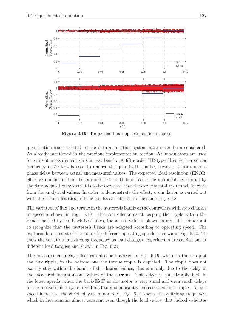
6.4 Experimental validation 127
0 0.02 0.04 0.06 0.08 0.1 0.120
0.2
0.4
0.6
0.8
1
Norm
aliz
edS
pee
d, F
lux
0 0.02 0.04 0.06 0.08 0.1 0.120
0.2
0.4
0.6
0.8
1
1.2
t (s)
Norm
aliz
edS
pee
d,T
orq
ue
Flux
Speed
Torque
Speed
Figure 6.19: Torque and flux ripple as function of speed
quantization issues related to the data acquisition system have never been considered.
As already mentioned in the previous implementation section, ∆Σ modulators are used
for current measurement on our test bench. A fifth-order IIR-type filter with a corner
frequency at 50 kHz is used to remove the quantization noise, however it introduces a
phase delay between actual and measured values. The expected ideal resolution (ENOB:
effective number of bits) lies around 10.5 to 11 bits. With the non-idealities caused by
the data acquisition system it is to be expected that the experimental results will deviate
from the analytical values. In order to demonstrate the effect, a simulation is carried out
with these non-idealities and the results are plotted in the same Fig. 6.18.
The variation of flux and torque in the hysteresis bands of the controllers with step changes
in speed is shown in Fig. 6.19. The controller aims at keeping the ripple within the
bands marked by the black bold lines, the actual value is shown in red. It is important
to recognize that the hysteresis bands are adapted according to operating speed. The
captured line current of the motor for different operating speeds is shown in Fig. 6.20. To
show the variation in switching frequency as load changes, experiments are carried out at
different load torques and shown in Fig. 6.21.
The measurement delay effect can also be observed in Fig. 6.19, where in the top plot
the flux ripple, in the bottom one the torque ripple is depicted. The ripple does not
exactly stay within the bands of the desired values; this is mainly due to the delay in
the measured instantaneous values of the current. This effect is considerably high in
the lower speeds, when the back-EMF in the motor is very small and even small delays
in the measurement system will lead to a significantly increased current ripple. As the
speed increases, the effect plays a minor role. Fig. 6.21 shows the switching frequency,
which in fact remains almost constant even though the load varies, that indeed validates

128 6 Design of Direct Torque Control on a FPGA
0 0.005 0.01 0.015 0.02
-5
0
5
10
t (s)0 0.005 0.01 0.015 0.02
-5
0
5
10
t (s)
0 0.005 0.01 0.015 0.02
-5
0
5
10
t (s)0 0.005 0.01 0.015 0.02
-5
0
5
10
t (s)
Speed=0.2 pu
i sa(A
)
i sa(A
)
i sa(A
)
i sa(A
)
Speed=0.4 pu
Speed=1 puSpeed=0.6 pu
Figure 6.20: Motor line current at different speeds
0.2 0.3 0.4 0.5 0.6 0.7 0.8 0.9 11
2
3
4
5
Normalized ω
TL=1 pu
TL=0.25 pu
TL=0.5 pu
f s(k
Hz)
Figure 6.21: Switching frequency variation with load torque (TL) as function of speed
the analytical findings. Even though the experimental results do not match exactly the
analytical investigations, they are indeed not faraway from the best-possible performance
of the PWM-based controls. A more detailed comparison with the PWM-based controls
will follow in the next section 6.4.1.
It is clearly visible that the differences seen here are neither due to the proposed control
strategy nor to the implementation on FPGA, but to the data acquisition system. It
is possible to achieve results very close to the presented analytical ones, provided the
designer takes care of the following:
• Minimize the delays in the measurement of analog signals as much as possible,
without compromising on the resolution at the same time.
• Avoid additional introduction of noise by improper routing.
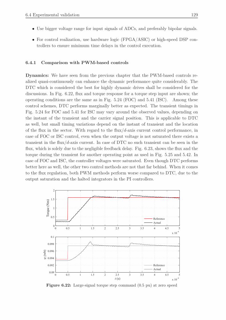
6.4 Experimental validation 129
• Use bigger voltage range for input signals of ADCs, and preferably bipolar signals.
• For control realization, use hardware logic (FPGA/ASIC) or high-speed DSP con-
trollers to ensure minimum time delays in the control execution.
6.4.1 Comparison with PWM-based controls
Dynamics: We have seen from the previous chapter that the PWM-based controls re-
alized quasi-continuously can enhance the dynamic performance quite considerably. The
DTC which is considered the best for highly dynamic drives shall be considered for the
discussions. In Fig. 6.22, flux and torque response for a torque step input are shown; the
operating conditions are the same as in Fig. 5.24 (FOC) and 5.41 (ISC). Among these
control schemes, DTC performs marginally better as expected. The transient timings in
Fig. 5.24 for FOC and 5.41 for ISC may vary around the observed values, depending on
the instant of the transient and the carrier signal position. This is applicable to DTC
as well, but small timing variations depend on the instant of transient and the location
of the flux in the sector. With regard to the flux/d-axis current control performance, in
case of FOC or ISC control, even when the output voltage is not saturated there exists a
transient in the flux/d-axis current. In case of DTC no such transient can be seen in the
flux, which is solely due to the negligible feedback delay. Fig. 6.23, shows the flux and the
torque during the transient for another operating point as used in Fig. 5.25 and 5.42. In
case of FOC and ISC, the controller voltages were saturated. Even though DTC performs
better here as well, the other two control methods are not that far behind. When it comes
to the flux regulation, both PWM methods perform worse compared to DTC, due to the
output saturation and the halted integrators in the PI controllers.
0 0.5 1 1.5 2 2.5 3 3.5 4 4.5 5
x 10-4
0
0.5
1
1.5
2
To
rqu
e (N
m)
Reference
Actual
0 0.5 1 1.5 2 2.5 3 3.5 4 4.5 5
x 10-4
0.09
0.092
0.094
0.096
0.098
0.1
t (s)
Reference
Actual
ψs(w
b)
Figure 6.22: Large-signal torque step command (0.5 pu) at zero speed
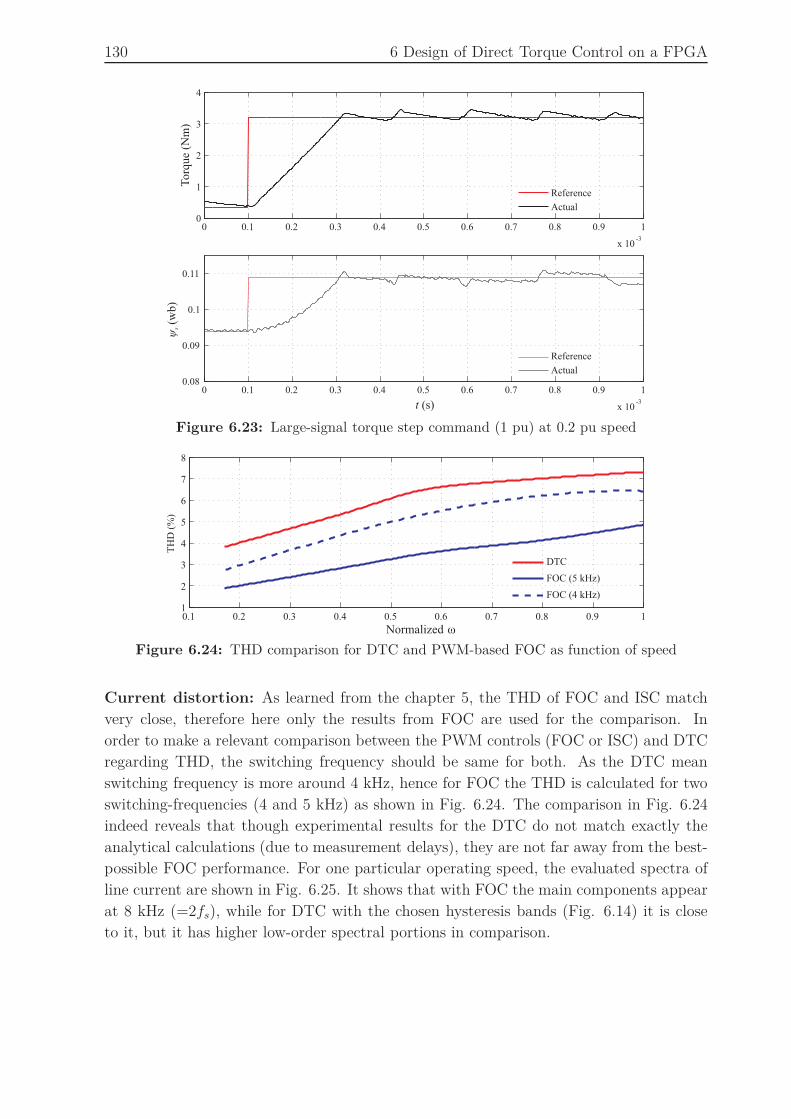
130 6 Design of Direct Torque Control on a FPGA
0 0.1 0.2 0.3 0.4 0.5 0.6 0.7 0.8 0.9 1
x 10-3
0
1
2
3
4
Torq
ue
(Nm
)Reference
Actual
0 0.1 0.2 0.3 0.4 0.5 0.6 0.7 0.8 0.9 1
x 10-3
0.08
0.09
0.1
0.11
t (s)
Reference
Actual
ψs(w
b)
Figure 6.23: Large-signal torque step command (1 pu) at 0.2 pu speed
0.1 0.2 0.3 0.4 0.5 0.6 0.7 0.8 0.9 11
2
3
4
5
6
7
8
Normalized ω
TH
D (
%)
DTC
FOC (5 kHz)
FOC (4 kHz)
Figure 6.24: THD comparison for DTC and PWM-based FOC as function of speed
Current distortion: As learned from the chapter 5, the THD of FOC and ISC match
very close, therefore here only the results from FOC are used for the comparison. In
order to make a relevant comparison between the PWM controls (FOC or ISC) and DTC
regarding THD, the switching frequency should be same for both. As the DTC mean
switching frequency is more around 4 kHz, hence for FOC the THD is calculated for two
switching-frequencies (4 and 5 kHz) as shown in Fig. 6.24. The comparison in Fig. 6.24
indeed reveals that though experimental results for the DTC do not match exactly the
analytical calculations (due to measurement delays), they are not far away from the best-
possible FOC performance. For one particular operating speed, the evaluated spectra of
line current are shown in Fig. 6.25. It shows that with FOC the main components appear
at 8 kHz (=2fs), while for DTC with the chosen hysteresis bands (Fig. 6.14) it is close
to it, but it has higher low-order spectral portions in comparison.
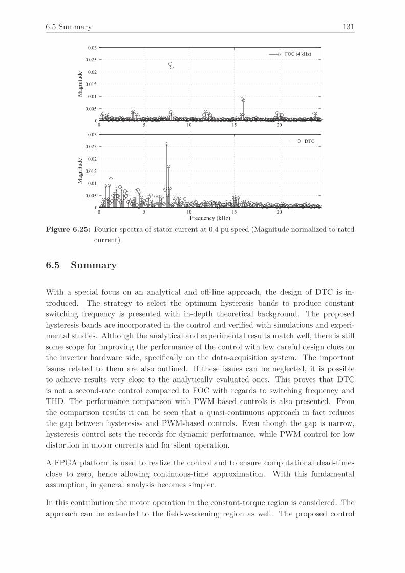
6.5 Summary 131
0 5 10 15 200
0.005
0.01
0.015
0.02
0.025
0.03
Mag
nit
ud
e
0 5 10 15 200
0.005
0.01
0.015
0.02
0.025
0.03
Frequency (kHz)
Mag
nit
ud
e
FOC (4 kHz)
DTC
Figure 6.25: Fourier spectra of stator current at 0.4 pu speed (Magnitude normalized to rated
current)
6.5 Summary
With a special focus on an analytical and off-line approach, the design of DTC is in-
troduced. The strategy to select the optimum hysteresis bands to produce constant
switching frequency is presented with in-depth theoretical background. The proposed
hysteresis bands are incorporated in the control and verified with simulations and experi-
mental studies. Although the analytical and experimental results match well, there is still
some scope for improving the performance of the control with few careful design clues on
the inverter hardware side, specifically on the data-acquisition system. The important
issues related to them are also outlined. If these issues can be neglected, it is possible
to achieve results very close to the analytically evaluated ones. This proves that DTC
is not a second-rate control compared to FOC with regards to switching frequency and
THD. The performance comparison with PWM-based controls is also presented. From
the comparison results it can be seen that a quasi-continuous approach in fact reduces
the gap between hysteresis- and PWM-based controls. Even though the gap is narrow,
hysteresis control sets the records for dynamic performance, while PWM control for low
distortion in motor currents and for silent operation.
A FPGA platform is used to realize the control and to ensure computational dead-times
close to zero, hence allowing continuous-time approximation. With this fundamental
assumption, in general analysis becomes simpler.
In this contribution the motor operation in the constant-torque region is considered. The
approach can be extended to the field-weakening region as well. The proposed control

132 6 Design of Direct Torque Control on a FPGA
strategy can be extended to any three-phase machine in general. E.g. it can be utilized
in case of induction machines wherein the analysis of the motor appears to be similar to
PMSM, provided the rotor flux is constant. The assumption of rotor flux being constant
is valid, because the time constant of the rotor flux is comparatively higher than that of
the stator. For steady-state operating conditions, with the stator-flux varying within the
small hysteresis band, really no considerable changes in the rotor flux show up.
133
7 Dynamically Reconfigurable Control Structures
The application of a FPGA in a control platform for the data acquisition and the control
realization has been explored in the previous chapters 4 and 5, 6, respectively. This
chapter will discuss the utilization of FPGA for realizing a reconfigurable control of AC
drives. The concept of dynamic reconfiguration is commonly known in Fault-Tolerant
Control (FTC) systems. In this chapter, the general idea of FTC is highlighted and
proposed so that it can be extended to achieve the optimal performance from a plant in
its whole operating region. Today, many industrial standard drives provide more than
one control scheme for their drive control. Customer may choose between, e.g., flux-
oriented control (FOC) and constant voltage-to-frequency ratio control (v/f). However,
dynamic (on-the fly) changeover between these control schemes is usually not available as
a feature, although it may be essential e.g. in cases of handling different operating modes
optimally or as a fallback strategy in case of faults. To be precise, the dynamic changeover
of control is in practice for specific purpose in traction drives since decades [JK1990].
The emphasis of this chapter is to present the generalized concept, implementation and
experimental validation of dynamic reconfiguration between well-known control schemes
for an induction machine. The idea is not only to show the switchover between the
different control schemes, but also to utilize field programmable gate array (FPGA) as
the basis for controller implementation. FPGAs capable of inherent parallel execution
make it easy to implement a dynamically reconfigurable control structure on a single
control platform.
7.1 Introduction
With the term “reconfigurable control” people start thinking about FTC [RP1997]. It
is because most of the research contributions to the FTC system utilize a reconfigurable
control as an integral part of the system [BP1997] [DT2008] [MR2002]. A FTC system is
defined as an intelligent system capable of reconfiguring its nominal control or dynamically
changing the control law to accommodate to a faulty condition [SF2001]. “Reconfigura-
tion” referred here is dynamic or online in nature; hence such a system can also be termed
as “dynamically reconfigurable system”.
For a particular plant or process, there may be several competitive control schemes which
show their strengths in different operating regions. A strategy to extract the best perfor-
mance out of a plant is to adopt the best control law depending on the operating point or
the operating condition. To achieve this, the system must have the capability to perform
dynamic reconfiguration between the control schemes. Hence, the above definition for

134 7 Dynamically Reconfigurable Control Structures
the reconfigurable control is more specific to a FTC system. Keeping the achievement of
optimal performance of a system as well in mind, the generalized definition for a dynami-
cally reconfigurable control can be given as “a control system which has one or more than
one independent control schemes and has the capability to modify within the nominal
control or changeover to other control online or dynamically” [MB2010] [MB2007]. Such
a generalized structure is shown in Fig. 7.1. In this the supervisory level is not only re-
sponsible for the fault diagnosis, but indeed also responsible to ensure the optimal control
performance. It does not only take the inputs from the plant and the controller but also
accepts interventions from the external user or an upper-level control system. Such an
user intervention can occur due to changing optimization goals during run-time.
A general concept to cope with changing optimization goals has been developed within the
Collaborative Research Center “Self-Optimizing Concepts and Structures in Mechanical
Engineering” funded by the Deutsche Forschungsgemeinschaft [SFB614]. A key element
of such a self-optimizing structure is called Operator Controller Module (OCM) [HO2004]
[BS2006], which is organized in different levels to cope with hard and weak real-time
requirements. On a cognitive or a supervisory level the system analysis, diagnosis, opti-
mization tasks and decisions on control reconfiguration are employed, while the control
tasks with hard real-time constraints are located on the controller level as shown in Fig.
7.1. The focus of this chapter is on the application of these general concepts of self-
optimization to the field of drive control, particularly to the dynamic changeover between
the control schemes for AC drives. Fault-diagnosis and fault-accommodation will not be
in the focus of this contribution.
A standard induction motor drive from the manufacturer comes mostly with v/f and
FOC control ([FB1972] [GL1980] [LE2001], most of the manufacturers) or Direct Torque
Control (DTC [TN1986] [DE1988] [ABB-01] [ABB-02]). These controls are implemented
on a microcontroller or a DSP. While FOC and DTC are well-known high-performance
drive controls, v/f control is commonly employed as low-performance drive control, often
seen in simple applications like pumps and fans, and also used as an intermediate step or
backup during the commissioning phase. Though many drive controllers provide several
variants of controls as menu, a changeover on-the-fly of controls is not available as a
Reconfiguration
- Fault diagnose- Optimal control str.
Supervisory system
Control 1Control 2
||
Control n
Plant(Actuator
and sensor)
Controllerlevel
Supervisorylevel
u*
y
x
Userinput
Figure 7.1: Generalized block diagram of dynamically reconfigurable control
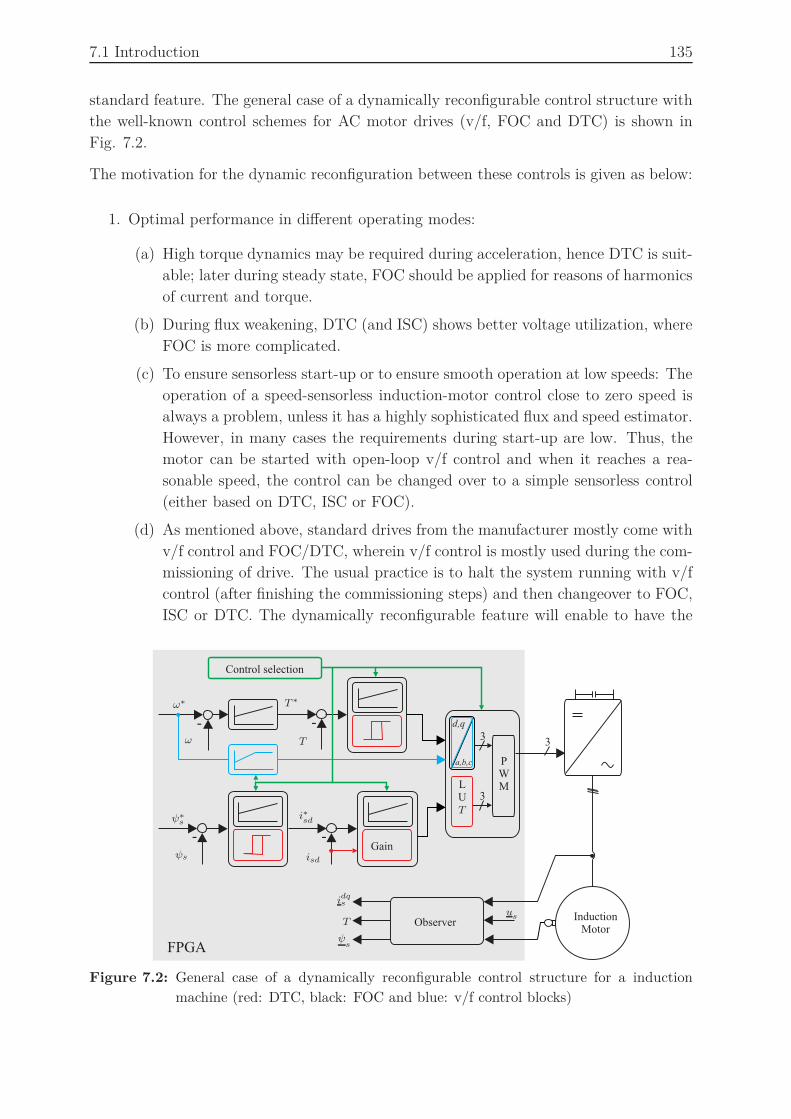
7.1 Introduction 135
standard feature. The general case of a dynamically reconfigurable control structure with
the well-known control schemes for AC motor drives (v/f, FOC and DTC) is shown in
Fig. 7.2.
The motivation for the dynamic reconfiguration between these controls is given as below:
1. Optimal performance in different operating modes:
(a) High torque dynamics may be required during acceleration, hence DTC is suit-
able; later during steady state, FOC should be applied for reasons of harmonics
of current and torque.
(b) During flux weakening, DTC (and ISC) shows better voltage utilization, where
FOC is more complicated.
(c) To ensure sensorless start-up or to ensure smooth operation at low speeds: The
operation of a speed-sensorless induction-motor control close to zero speed is
always a problem, unless it has a highly sophisticated flux and speed estimator.
However, in many cases the requirements during start-up are low. Thus, the
motor can be started with open-loop v/f control and when it reaches a rea-
sonable speed, the control can be changed over to a simple sensorless control
(either based on DTC, ISC or FOC).
(d) As mentioned above, standard drives from the manufacturer mostly come with
v/f control and FOC/DTC, wherein v/f control is mostly used during the com-
missioning of drive. The usual practice is to halt the system running with v/f
control (after finishing the commissioning steps) and then changeover to FOC,
ISC or DTC. The dynamically reconfigurable feature will enable to have the
-
PWM
InductionMotor
Observer
-
3
-
-
Gain
LU
a,b,c
d,q
33
Control selection
FPGA
ω∗
ω
T ∗
T
T
T
ψ∗
s
ψs
i∗sd
isd
ψs
idqsus
Figure 7.2: General case of a dynamically reconfigurable control structure for a induction
machine (red: DTC, black: FOC and blue: v/f control blocks)
136 7 Dynamically Reconfigurable Control Structures
dynamic switch-over of controls under such conditions. This adds an advanced
feature to the drive, while yielding greater flexibility to the user.
2. Fallback strategy in cases of faults and failures (supervisory system): High-
performance drives which are used as highly reliable systems in application fields
such as power plants are never allowed to halt unless planned. Failures due to a
sensor or the closed-loop control would shutdown the system. Under such a sce-
nario, the proposed reconfigurable system with an open-loop v/f control could be
used as a fallback strategy to continue operation with a reduced performance. In
this particular case v/f control acts as the “supervisory control”.
Among the control schemes used in the general case of reconfigurable structures (Fig.
7.2), FOC is the most complicated and uses the most resources. Hence, it is used as
the base platform and over that the other schemes are superimposed, to make it better
understandable. Only v/f control falls out from these schemes because of its simple open-
loop structure. The block “Control selection” seen in Fig. 7.2 does not only switch the
control schemes, but also initializes the controllers with appropriate values. The “Control
selection” is triggered by the supervisory system; the cause for the trigger could be due
to the operating point of the plant or from an external user or the upper-level control
input. The easier way to present this general case is by dividing the task into the following
sections based on the control schemes used:
1. Reconfiguration between high-performance control schemes.
2. Reconfiguration between a low- and a high-performance control scheme.
The first part of the chapter considers the dynamic reconfiguration of two high-
performance controls. In this, one can have the wider option to choose two among many
variants of control schemes. Combination may be just within the variants of FOC (e.g.
stator-flux-oriented control, rotor-flux-oriented control etc.) or within the variants of
DTC (e.g. hysteresis DTC, ISC etc.) or it could be a variant of a FOC and a DTC. For
demonstration rotor-flux-oriented control and ISC (Indirect Stator-quantity Control) are
selected. For instance, ISC is also commonly known as PWM-DTC or SVM-DTC (Space-
Vector Modulated DTC). Rotor-flux-oriented control utilizes the rotor-flux-orientation to
implement standard PI current controllers to regulate the rotor-flux amplitude and the
torque of the motor. In case of ISC, the torque is controlled by the angle between stator-
and rotor-flux, and stator-flux magnitude is regulated with the feed-forward voltage terms.
These control schemes together form very challenging combination, because FOC regulates
the rotor flux while DTC the stator flux. Hence, there is always a disturbance on the flux
whenever a changeover of control takes place. This is due to a difference in the magnitude
of these flux values.
The second part of the chapter considers the dynamic reconfiguration of a low-performance
and a high-performance control scheme. The best choice for a low-performance control
7.2 Dynamic reconfiguration between high-performance control schemes 137
scheme is open-loop v/f control. The other control scheme can be chosen among the long
list of high-performance controls. Keeping one of the motivations in mind, the operation
of induction machine close to zero-speed, a simple sensorless scheme based on FOC is
chosen as the high-performance control. The required estimation of the flux vector and
the motor speed to incorporate sensorless FOC is done with the help of a voltage- or
stator-model-based flux observer [HB1973], which is also known as inherently sensorless
observer [JH2006].
7.2 Dynamic reconfiguration between high-performance control
schemes
The rotor-flux-oriented control and the ISC for an induction-motor drive are the selected
control schemes to demonstrate the reconfiguration between two high-performance con-
trols. To simplify explanation, in this whole section the rotor-flux-oriented control is
abbreviated as FOC. It utilizes the rotor-flux-orientation to implement the current con-
troller, while in ISC there is no specific current controller based on a feed-forward-type of
control. To incorporate the feedback signals for these controls, it is essential to know the
magnitude and position of the stator-flux and the rotor-flux vector. To estimate them, a
closed-loop full-order observer with the stator-flux and the rotor-flux vector as state vari-
ables is utilized. This part of the chapter is organized as follows: The basic arrangement
of the control schemes is explained with the help of a block diagram in section 7.2.1, the
implementation details and space characterization on FPGA and the dynamic reconfig-
urable feature are given in section 7.2.2 and detailed experimental results are presented
in section 7.2.3.
7.2.1 Basic arrangement
The individual block diagrams of FOC and ISC are shown in Fig. 7.3(a) and 7.3(b),
respectively. To incorporate FOC it is essential to evaluate the position of the rotor-flux
vector in stator coordinates and its magnitude. For ISC the estimate of the stator-flux
vector is required. In case of an induction machine the estimation of a single flux vector
or both the stator-flux and the rotor-flux vector does not make much difference, other
than few more additional simple arithmetic operations. There are many options to choose
the flux observer [MB2007] to estimate these vectors. In this particular application a full-
order Luenberger-type observer with the stator- and the rotor-flux vector as the state
variables is chosen. This acts as a common observer for both the controls, as it can be
seen in Fig. 7.3.
Motor modeling and observer:
The complex representation of the different reference frames of an induction motor is
shown in Fig. 7.4. The voltage equations of an induction machine in stator coordinates

138 7 Dynamically Reconfigurable Control Structures
PWM
InductionMotor
Luenbergerobserver
- -
a,b,c
d,q
3 3
- -
Est
imat
ion
Vff
Vff
ω∗
ω
i∗sq
isq
ψ∗
r
ψr
i∗sd
isd
is
usψr
ψs
θr
(a) Block diagram of FOC
PWM
InductionMotor
Luenbergerobserver
- -3 3
Est
imat
ion
Volt
age
vec
tor
gen
erat
ionω∗
ω
T ∗
T
δ∗
T
ψ∗
s
is
usψr
ψs
θr
(b) Block diagram of ISC
Figure 7.3: Block schematic of FOC and ISC for induction motor drive
α
β
αr
βr
d
q
x
y
θr ǫ
δTψ r
ψ s
is
Figure 7.4: Complex representation of various reference frames of induction machine
(α/β: Stator coordinates, αr/βr: Rotor coordinates, d/q: Rotor-flux coordinates,
x/y: Stator-flux coordinates)
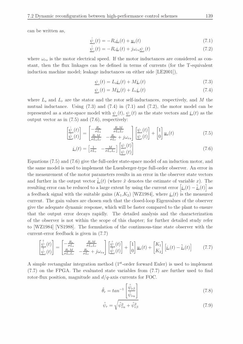
7.2 Dynamic reconfiguration between high-performance control schemes 139
can be written as,
ψs(t) = −Rsis(t) + us(t) (7.1)
ψr(t) = −Rrir(t) + jωrsψr(t) (7.2)
where ωrs is the motor electrical speed. If the motor inductances are considered as con-
stant, then the flux linkages can be defined in terms of currents (for the T-equivalent
induction machine model; leakage inductances on either side [LE2001]),
ψs(t) = Lsis(t) + Mir(t) (7.3)
ψr(t) = Mis(t) + Lrir(t) (7.4)
where Ls and Lr are the stator and the rotor self-inductances, respectively, and M the
mutual inductance. Using (7.3) and (7.4) in (7.1) and (7.2), the motor model can be
represented as a state-space model with ψs(t), ψ
r(t) as the state vectors and is(t) as the
output vector as in (7.5) and (7.6), respectively:
[
ψs(t)
ψr(t)
]
=
− RsσLs
RsMσLsLr
RrMσLsLr
− RrσLr
+ jωrs
[
ψs(t)
ψr(t)
]
+
[
1
0
]
us(t) (7.5)
is(t) =[
1σLs
− MσLsLr
][
ψs(t)
ψr(t)
]
(7.6)
Equations (7.5) and (7.6) give the full-order state-space model of an induction motor, and
the same model is used to implement the Luenberger-type full-order observer. An error in
the measurement of the motor parameters results in an error in the observer state vectors
and further in the output vector is(t) (where x denotes the estimate of variable x). The
resulting error can be reduced to a large extent by using the current error[
is(t) − is(t)]
as
a feedback signal with the suitable gains (K1,K2) [WZ1984], where is(t) is the measured
current. The gain values are chosen such that the closed-loop Eigenvalues of the observer
give the adequate dynamic response, which will be faster compared to the plant to ensure
that the output error decays rapidly. The detailed analysis and the characterization
of the observer is not within the scope of this chapter; for further detailed study refer
to [WZ1984] [VS1988]. The formulation of the continuous-time state observer with the
current-error feedback is given in (7.7)
ˆψs(t)
ˆψr(t)
=
− RsσLs
RsMσLsLr
RrMσLsLr
− RrσLr
+ jωrs
[
ψs(t)
ψr(t)
]
+
[
1
0
]
us(t) +
[
K1
K2
][
is(t) − is(t)]
(7.7)
A simple rectangular integration method (1st-order forward Euler) is used to implement
(7.7) on the FPGA. The evaluated state variables from (7.7) are further used to find
rotor-flux position, magnitude and d/q-axis currents for FOC.
θr = tan−1
ψrβ
ψrα
(7.8)
ψr =
√
ψ2rα + ψ2
rβ (7.9)

140 7 Dynamically Reconfigurable Control Structures
isd = isαcos(θr) + isβsin(θr)
isq = −isαsin(θr) + isβcos(θr)(7.10)
The additional torque estimate essential for ISC is evaluated using one of the following
two equations,
T =3
2p[
ψsαisβ − ψsβisα]
=3
2p
[
(1 − σ)LsM
ψr isq
] (7.11)
where p is the number of pole pairs of the motor.
Control schemes:
In chapter 5, the detailed control principles of FOC and ISC have been covered for the
PMSM, hence here we will go through in brief for the induction machine.
FOC: It is a decoupled controller, where torque and flux magnitude are controlled inde-
pendently with the help of flux orientation. Based on this principle, in rotor-flux-oriented
control the torque and rotor-flux magnitude are regulated by controlling the stator-current
vector in regard to the rotor-flux axis accordingly. The current component aligned with
the flux axis is called the d-axis current isd and the quadrature component the q-axis cur-
rent isq. The current component isd controls the magnitude of rotor-flux and isq controls
the torque. To regulate these currents, PI controllers are used as shown in Fig. 7.3(a).
Controllers are designed using the Magnitude Optimum method with the assumption of
compensating the feed-forward terms (Vff) exactly in the control loop. Vff refers to the
cross-coupling via Ls and the back-EMF in the d/q -axis voltage expressions, highlighted
by curly brackets in (7.12).
usd = Rsisd + σLsisd − σLsωθr isq + (1 − σ)LsM
ˆψr︸ ︷︷ ︸
usq = Rsisq + σLsisq + σLsωθr isd + (1 − σ)LsMψrωθr
︸ ︷︷ ︸
(7.12)
where ωθr is the angular velocity of the rotor flux in stator coordinates. In principle, it is
possible to incorporate the control without compensating the Vff terms, however better
dynamics will result if these terms are compensated.
ISC: Unlike FOC with the stator current as the inner control objective, the original DTC
[TN1986] or DSC [DE1988] governs the torque by means of controlling the angle between
the stator flux and the rotor flux vectors. The idea of this torque control is retained in
ISC with the feed-forward type of flux control. In contrast to original DTC, ISC yields
a constant switching-frequency. The torque equation given in (7.11) can be extended to
represent it in terms of stator flux and rotor flux as in (7.13).
T =3
2p
M
σLsLrψrψssin(δT ) (7.13)

7.2 Dynamic reconfiguration between high-performance control schemes 141
where δT is called the torque angle, i.e. the angle between the stator and the rotor flux
vectors, which is shown in Fig. 7.4. Depending on the torque-controller output (i.e. δ∗T
shown in Fig. 7.3(b)) the flux-reference value for the motor can be evaluated as,
ψ∗
s= ψ∗
sejθ∗
s (7.14)
where θ∗s = θr + δ∗
T . Then, with the help of polar-to-cartesian transformation, the α, β
components of the stator-flux reference values can be evaluated directly from (7.14), and
correspondingly the required voltage-vector reference components are,
u∗sα =
ψ∗sα − ψsαTs
+ isαRs
u∗sβ =
ψ∗sβ − ψsβ
Ts+ isβRs
(7.15)
where Ts is the sample period. The controller design procedures for FOC and ISC have
been already discussed in chapter 5, hence will not be covered here again.
Dynamically reconfigurable control structure: It is possible to merge the above
discussed control schemes with some of the controller modules in common (like speed and
torque PI controller) and the common observer. From Fig. 7.3(a) and 7.3(b), FOC looks
more complex and requires a higher number of modules compared to ISC. Hence, while
merging these two controls to form a multiple control structure, FOC is used as the base
platform and over that ISC is superimposed. In the process an attempt is made to utilize
the maximum possible common resources. Such a structure is shown in Fig. 7.5, where
the blue-colored modules and lines are the only structure added to FOC to incorporate
ISC. In the structure, the switch-over between these control schemes is done with the help
of “Control selection” (represented in green line). The task of this signal is to initiate
the process of changeover; the trigger instant of the signal is arbitrary. Initialization and
parameter adaptation for the controllers is done within their structures; details will follow
in the implementation section.
7.2.2 Implementation
The proposed reconfigurable structure shown in Fig. 7.5 is implemented on a Xilinx
Vertex-2P-XC2VP20 FPGA, which is the same platform that was utilized in the previous
chapters. To develop the logic, the Xilinx System-Generator tool on the Matlab-Simulink
platform is used. The implementation details for the observer and the controls are shown
in Fig. 7.6 and 7.7, respectively. The block schematics are shown instead of screen shots of
Simulink files, because they are more suited to understand the complex multiple control
structure. The bit-width and the binary position of most of variables and the needed
resources are given in these figures. E.g. in Fig. 7.6 the voltage vector us is represented
in the format of [16.14], same as Q16.14: Fixed-point representation with bit-width of
16 and binary point after the 14th bit. With this binary representation it is possible
to represent a value scale up to ±2 pu as this avoids the overflow in most cases. The
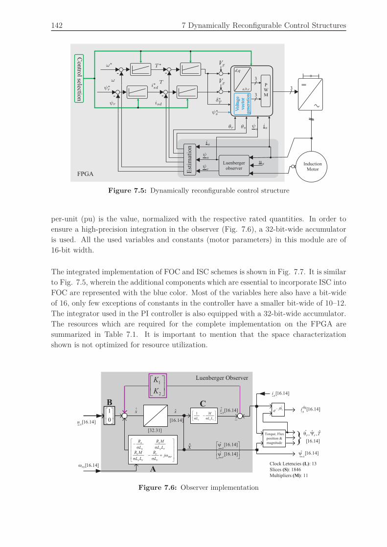
142 7 Dynamically Reconfigurable Control Structures
Co
ntro
l selection
FPGA
PWM
InductionMotor
Luenbergerobserver
- -
a,b,c
d,q
3
3
- -
Est
imat
ion
Vff
Vo
ltag
ev
ecto
rg
ener
atio
n 3
Vff
ω∗
ω
T ∗
Tψ∗
r
ψr
i∗sd
isd
is
is
usψr
ψs
ψs
θr θs
ψ∗
s
δ∗
T
Figure 7.5: Dynamically reconfigurable control structure
per-unit (pu) is the value, normalized with the respective rated quantities. In order to
ensure a high-precision integration in the observer (Fig. 7.6), a 32-bit-wide accumulator
is used. All the used variables and constants (motor parameters) in this module are of
16-bit width.
The integrated implementation of FOC and ISC schemes is shown in Fig. 7.7. It is similar
to Fig. 7.5, wherein the additional components which are essential to incorporate ISC into
FOC are represented with the blue color. Most of the variables here also have a bit-wide
of 16, only few exceptions of constants in the controller have a smaller bit-wide of 10–12.
The integrator used in the PI controller is also equipped with a 32-bit-wide accumulator.
The resources which are required for the complete implementation on the FPGA are
summarized in Table 7.1. It is important to mention that the space characterization
shown is not optimized for resource utilization.
]14.16[ˆs
i
-
úú
û
ù
êê
ë
é
]14.16[ˆ
]14.16[ˆ
r
s
y
y
úû
ùêë
é
2
1
K
K
úû
ùêë
é0
1
Clock Letencies (L): 13
Slices (S): 1846
Multipliers (M): 11
]31.32[
úû
ùêë
é-
rss LL
M
L ss
1
A
B C
]14.16[
x& x
x
Torque, Flux
position &
magnitude
rje
q-
]14.16[
ˆ,ˆ,ˆ Trr Yq
]14.16[ˆs
y
]14.16[dq
si
]14.16[s
i
Luenberger Observer
]14.16[s
u
]14.16[rsw
úúúú
û
ù
êêêê
ë
é
+-
-
mrr
r
rs
r
rs
s
s
s
jL
R
LL
MR
LL
MR
L
R
wss
ss
Figure 7.6: Observer implementation
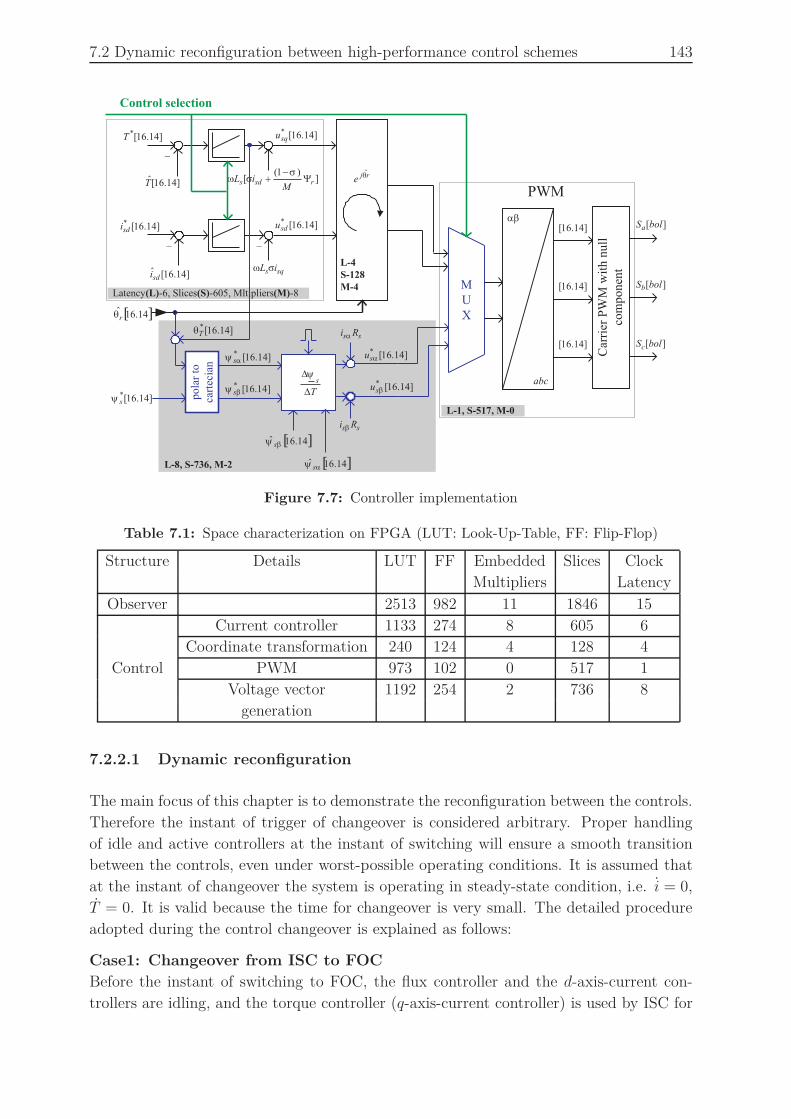
7.2 Dynamic reconfiguration between high-performance control schemes 143
rje q
L-4
S-128
M-4
-
]14.16[*T
]14.16[T ])1(
[ rsdsM
iL Y-
+s
sw
-
sqs iL sw]14.16[ˆ
sdi
]14.16[*sdi
Latency(L)-6, Slices(S)-605, Mltipliers(M)-8
]14.16[*squ
]14.16[*sdu
-
[ ]14.16ˆrq
ab
abc
]14.16[
]14.16[
]14.16[
Car
rier
PW
Mw
ith
nu
ll
com
pon
ent
][bolSb
][bolSc
][bolSa
]14.16[*Tq
]14.16[*sy p
ola
rto
cart
ecia
n
]14.16[*ay s
]14.16[*by s
[ ]14.16ˆ ay s
[ ]14.16ˆ by s
T
s
D
Dy
ss Ri a
ss Ri b
M
U
X
]14.16[*asu
]14.16[*bsu
L-8, S-736, M-2
Control selection
PWM
L-1, S-517, M-0
Figure 7.7: Controller implementation
Table 7.1: Space characterization on FPGA (LUT: Look-Up-Table, FF: Flip-Flop)
Structure Details LUT FF Embedded Slices Clock
Multipliers Latency
Observer 2513 982 11 1846 15
Current controller 1133 274 8 605 6
Coordinate transformation 240 124 4 128 4
Control PWM 973 102 0 517 1
Voltage vector 1192 254 2 736 8
generation
7.2.2.1 Dynamic reconfiguration
The main focus of this chapter is to demonstrate the reconfiguration between the controls.
Therefore the instant of trigger of changeover is considered arbitrary. Proper handling
of idle and active controllers at the instant of switching will ensure a smooth transition
between the controls, even under worst-possible operating conditions. It is assumed that
at the instant of changeover the system is operating in steady-state condition, i.e. i = 0,
T = 0. It is valid because the time for changeover is very small. The detailed procedure
adopted during the control changeover is explained as follows:
Case1: Changeover from ISC to FOC
Before the instant of switching to FOC, the flux controller and the d-axis-current con-
trollers are idling, and the torque controller (q-axis-current controller) is used by ISC for
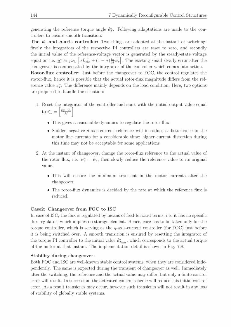
144 7 Dynamically Reconfigurable Control Structures
generating the reference torque angle δ∗T . Following adaptations are made to the con-
trollers to ensure smooth transition:
The d- and q-axis controller: Two things are adopted at the instant of switching;
firstly the integrators of the respective PI controllers are reset to zero, and secondly
the initial value of the reference-voltage vector is generated by the steady-state voltage
equation i.e. u∗s ≈ jωθr
[
σLsis + (1 − σ)LsMψr]
. The existing small steady error after the
changeover is compensated by the integrator of the controller which comes into action.
Rotor-flux controller: Just before the changeover to FOC, the control regulates the
stator-flux, hence it is possible that the actual rotor-flux magnitude differs from the ref-
erence value ψ∗r . The difference mainly depends on the load condition. Here, two options
are proposed to handle the situation:
1. Reset the integrator of the controller and start with the initial output value equal
to i∗sd =[
ψ∗
r−ψrM
]
• This gives a reasonable dynamics to regulate the rotor flux.
• Sudden negative d-axis-current reference will introduce a disturbance in the
motor line currents for a considerable time; higher current distortion during
this time may not be acceptable for some applications.
2. At the instant of changeover, change the rotor-flux reference to the actual value of
the rotor flux, i.e. ψ∗r = ψr, then slowly reduce the reference value to its original
value.
• This will ensure the minimum transient in the motor currents after the
changeover.
• The rotor-flux dynamics is decided by the rate at which the reference flux is
reduced.
Case2: Changeover from FOC to ISC
In case of ISC, the flux is regulated by means of feed-forward terms, i.e. it has no specific
flux regulator, which implies no storage element. Hence, care has to be taken only for the
torque controller, which is serving as the q-axis-current controller (for FOC) just before
it is being switched over. A smooth transition is ensured by resetting the integrator of
the torque PI controller to the initial value δ∗Tinit
, which corresponds to the actual torque
of the motor at that instant. The implementation detail is shown in Fig. 7.8.
Stability during changeover:
Both FOC and ISC are well-known stable control systems, when they are considered inde-
pendently. The same is expected during the transient of changeover as well. Immediately
after the switching, the reference and the actual value may differ, but only a finite control
error will result. In succession, the activated control scheme will reduce this initial control
error. As a result transients may occur, however such transients will not result in any loss
of stability of globally stable systems.

7.2 Dynamic reconfiguration between high-performance control schemes 145
]14.16[*T
]14.16[T
]14.16[*Td
PI Controller
Kp
Trigger pulse
Switching signal
TTinitdd ˆ* =
-
Figure 7.8: Torque controller at the instant of changeover from FOC to ISC
7.2.3 Experimental validation
The experimental test bench consists of an induction motor and a permanent-magnet
synchronous motor (PMSM) setup, same as used in the previous investigations. The
difference exists in the purpose of these machines; here the PMSM is used as the load
machine and the induction machine as the specimen (test object). The load machine can
be programmed either in the speed- or the torque-controlled mode. The arrangement of
the test bench and the details of the motors are outlined in the Appendix A.1.
Robustness and smoothness of changeover can be observed by monitoring the motor
torque, the flux and the line currents. To be more specific, the torque and the stator-flux
value during the changeover demonstrate the robustness of the controllers, and the motor
currents yield the information whether the transients are well within the allowed range
during the changeover. This can be tested in two different ways: 1) Operate the setup
at constant torque by the load machine and control the speed by the specimen and 2)
Operate the setup at constant speed by the load machine and control the torque from the
specimen. The torque and flux behavior of the specimen cannot be identified properly
when it is running in the speed-controlled mode. Hence, the second option is more suitable
to do thorough observations of the controllers.
The instant of changeover of the control is arbitrary (no explicit supervisory system
is considered); it can appear at any instant in the whole operating region of the motor.
Therefore the dynamic reconfiguration is demonstrated at various speeds and load torques.
Figs. 7.9, 7.10 and 7.11 correspond to the measurements at 0 pu, 0.5 pu and 1 pu of speed
respectively. At every speed it is tested for two different load conditions: One at rated
torque (1 pu=1.7 Nm) and the other at two times the rated torque (2 pu=3.4 Nm). All
the figures are similar in structure, made up of four parts viz, left top: Changeover from
ISC to FOC at rated torque, right top: Changeover from FOC to ISC at rated torque,
left bottom: Changeover from ISC to FOC at double the rated torque, right bottom:
Changeover from FOC to ISC at double the rated torque.
Changeover from ISC to FOC: In all the Figs. 7.9, 7.10 and 7.11, the left top and
bottom plot show the response of the torque, the stator flux and the three line currents
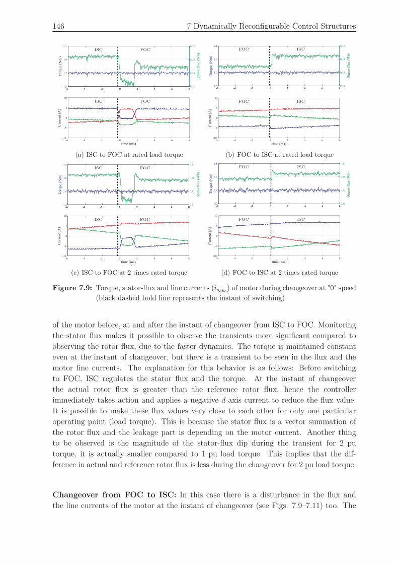
146 7 Dynamically Reconfigurable Control Structures
-6 -4 -2 0 2 4 6 81.5
1.7
1.9
2.1
To
rqu
e (N
m)
-6 -4 -2 0 2 4 6 80.31
0.33
0.35
0.37
-6 -4 -2 0 2 4 6 8-10
-5
0
5
10
time (ms)
Cu
rren
t (A
)
Sta
tor
flu
x (
Wb
)
ISC
ISC
FOC
FOC
(a) ISC to FOC at rated load torque
-6 -4 -2 0 2 4 6 81.5
1.7
1.9
2.1
To
rqu
e (N
m)
-6 -4 -2 0 2 4 6 80.31
0.33
0.35
0.37
-6 -4 -2 0 2 4 6 8-10
-5
0
5
10
time (ms)
Cu
rren
t (A
)
Sta
tor
flu
x (
Wb
)
ISC
ISC
FOC
FOC
(b) FOC to ISC at rated load torque
-6 -4 -2 0 2 4 6 83.2
3.4
3.6
3.8
Torq
ue
(Nm
)
-6 -4 -2 0 2 4 6 80.31
0.33
0.35
0.37
-6 -4 -2 0 2 4 6 8-10
-5
0
5
10
time (ms)
Curr
ent
(A)
Sta
tor
flux (
Wb)
ISC
ISC
FOC
FOC
(c) ISC to FOC at 2 times rated torque
-6 -4 -2 0 2 4 6 83.2
3.4
3.6
3.8
To
rqu
e (N
m)
-6 -4 -2 0 2 4 6 80.31
0.33
0.35
0.37
-6 -4 -2 0 2 4 6 8-10
-5
0
5
10
time (ms)
Cu
rren
t (A
)
Sta
tor
flu
x (
Wb
)
ISC
ISC
FOC
FOC
(d) FOC to ISC at 2 times rated torque
Figure 7.9: Torque, stator-flux and line currents (isabc) of motor during changeover at "0" speed
(black dashed bold line represents the instant of switching)
of the motor before, at and after the instant of changeover from ISC to FOC. Monitoring
the stator flux makes it possible to observe the transients more significant compared to
observing the rotor flux, due to the faster dynamics. The torque is maintained constant
even at the instant of changeover, but there is a transient to be seen in the flux and the
motor line currents. The explanation for this behavior is as follows: Before switching
to FOC, ISC regulates the stator flux and the torque. At the instant of changeover
the actual rotor flux is greater than the reference rotor flux, hence the controller
immediately takes action and applies a negative d-axis current to reduce the flux value.
It is possible to make these flux values very close to each other for only one particular
operating point (load torque). This is because the stator flux is a vector summation of
the rotor flux and the leakage part is depending on the motor current. Another thing
to be observed is the magnitude of the stator-flux dip during the transient for 2 pu
torque, it is actually smaller compared to 1 pu load torque. This implies that the dif-
ference in actual and reference rotor flux is less during the changeover for 2 pu load torque.
Changeover from FOC to ISC: In this case there is a disturbance in the flux and
the line currents of the motor at the instant of changeover (see Figs. 7.9–7.11) too. The

7.2 Dynamic reconfiguration between high-performance control schemes 147
-6 -4 -2 0 2 4 6 81.5
1.7
1.9
2.1
To
rqu
e (N
m)
-6 -4 -2 0 2 4 6 80.31
0.33
0.35
0.37
-6 -4 -2 0 2 4 6 8-10
-5
0
5
10
time (ms)
Cu
rren
t (A
)
Sta
tor
flu
x (
Wb
)
ISC
ISC
FOC
FOC
(a) ISC to FOC at rated load torque
-6 -4 -2 0 2 4 6 81.5
1.7
1.9
2.1
To
rqu
e (N
m)
-6 -4 -2 0 2 4 6 80.31
0.33
0.35
0.37
-6 -4 -2 0 2 4 6 8-10
-5
0
5
10
time (ms)
Cu
rren
t (A
)
Sta
tor
flu
x (
Wb
)
ISC
ISC
FOC
FOC
(b) FOC to ISC at rated load torque
-6 -4 -2 0 2 4 6 83.2
3.4
3.6
3.8
To
rqu
e (N
m)
-6 -4 -2 0 2 4 6 80.31
0.33
0.35
0.37
-6 -4 -2 0 2 4 6 8-10
-5
0
5
10
time (ms)
Cu
rren
t (A
)
Sta
tor
flu
x (
Wb
)
ISC
ISC
FOC
FOC
(c) ISC to FOC at 2 times rated torque
-6 -4 -2 0 2 4 6 83.2
3.4
3.6
3.8
To
rqu
e (N
m)
-6 -4 -2 0 2 4 6 80.31
0.33
0.35
0.37
-6 -4 -2 0 2 4 6 8-10
-5
0
5
10
time (ms)
Cu
rren
t (A
)
Sta
tor
flu
x (
Wb
)
ISC
ISC
FOC
FOC
(d) FOC to ISC at 2 times rated torque
Figure 7.10: Torque, stator-flux and line currents (isabc) of motor during changeover at "0.5
pu" speed (black dashed bold line represents the instant of switching)
nature of disturbance is different as seen with a very small duration, compared to the
previous case. This is due to the following reasons:
• The dynamics of the stator flux is much faster, compared to the rotor flux: Due to
the smaller stator time constant compared to the rotor time constant.
• In case of ISC, the flux is regulated by means of feed-forward terms, no PI controller
imposes an additional delay for the control.
The transients associated with both changeovers appears to be smooth and acceptable
in most applications. However, there are few exceptional applications which may not
be acceptable due to a long-period disturbance in the line currents and therefore higher
distortion and interference issue; specifically pointing to the changeover from ISC to FOC.
To solve this issue one can use the strategy proposed in section 7.2.2.1, which does the
adaptation of the rotor-flux reference value to ensure a smooth transition. The responses
corresponding to this strategy are shown in Fig. 7.12. In the figure it is clearly visible
that there is no transient seen in the stator flux as well as in the line currents during the
changeover.

148 7 Dynamically Reconfigurable Control Structures
-6 -4 -2 0 2 4 6 81.5
1.7
1.9
2.1
Torq
ue
(Nm
)
-6 -4 -2 0 2 4 6 80.31
0.33
0.35
0.37
-6 -4 -2 0 2 4 6 8-10
-5
0
5
10
time (ms)
Curr
ent
(A)
Sta
tor
flux (
Wb)
ISC
ISC
FOC
FOC
(a) ISC to FOC at rated load torque
-6 -4 -2 0 2 4 6 81.5
1.7
1.9
2.1
Torq
ue
(Nm
)
-6 -4 -2 0 2 4 6 80.31
0.33
0.35
0.37
-6 -4 -2 0 2 4 6 8-10
-5
0
5
10
time (ms)
Curr
ent
(A)
Sta
tor
flux (
Wb)
ISC
ISC
FOC
FOC
(b) FOC to ISC at rated load torque
-6 -4 -2 0 2 4 6 83.2
3.4
3.6
To
rqu
e (N
m)
-6 -4 -2 0 2 4 6 80.31
0.33
0.35
0.37
-6 -4 -2 0 2 4 6 8-10
-5
0
5
10
time (ms)
Cu
rren
t (A
)
Sta
tor
flu
x (
Wb
)
ISC
ISC
FOC
FOC
(c) ISC to FOC at 2 times rated torque
-6 -4 -2 0 2 4 6 83.2
3.4
3.6
Torq
ue (
Nm
)
-6 -4 -2 0 2 4 6 80.31
0.33
0.35
0.37
-6 -4 -2 0 2 4 6 8-10
-5
0
5
10
time (ms)
Curr
ent (A
)
Sta
tor
flu
x (
Wb
)
ISC
ISC
FOC
FOC
(d) FOC to ISC at 2 times rated torque
Figure 7.11: Torque, stator-flux and line currents (isabc) of motor during changeover at “1 pu”
speed (black dashed bold line represents the instant of switching)
-6 -4 -2 0 2 4 6 81.5
1.7
1.9
2.1
Torq
ue
(Nm
)
-6 -4 -2 0 2 4 6 80.31
0.33
0.35
0.37
-6 -4 -2 0 2 4 6 8-10
-5
0
5
10
time (ms)
Curr
ent
(A)
Sta
tor
flux (
Wb)
ISC
ISC
FOC
FOC
Figure 7.12: Torque, stator-flux and line currents (isabc) of motor during changeover at "0"
speed with 1 pu torque (black dashed bold line represents the instant of switching)

7.3 Dyn. reconfiguration between low-performance and high performance control 149
7.3 Dynamic reconfiguration between a low-performance and a
high-performance control scheme
The open-loop v/f control and a simple sensorless FOC are the selected control schemes
to demonstrate the concept of dynamic reconfiguration between a low-performance and
a high-performance control scheme. V/f control is the most popular control scheme for
low-performance induction motor drives in the industry. Similarly the sensorless FOC
scheme based on the voltage or the stator model for the flux observation is also very well
addressed. The stator- or the voltage-model-based observer is used to incorporate the
flux orientation as well as the speed-sensorless operation. The voltage-based observer is
inherently sensorless and very simple in terms of implementation. The observer works
very satisfactorily in the whole operating region except at and around zero speed.
7.3.1 Basic arrangement
In this section, individual control schemes are explained with the help of block diagrams,
followed by theoretical details of the implementation of the reconfigurable system and the
aspect of handling the transient of switching with stability issues.
Sensorless FOC: The arrangement of the FOC scheme is very well known; the block
diagram representation is shown in Fig. 7.13, which is not very different from Fig. 7.3(a).
The detailed explanation for the control part of FOC is not necessary, as it has already
been outlined in the previous section. To incorporate the speed-sensorless operation, it
is essential to have the direct flux-orientation (DFOC) for the control, which requires a
flux observer. Many flux observers have been proposed for sensorless operation [JH2006].
Among all, the voltage-model-based observer which is inherently speed-sensorless is the
simplest one. This was the first flux estimator to be utilized in the early 1970s [HB1973]
to incorporate the observer-based DFOC.
PWM
InductionMotor
- -
a,b,c
d,q
3 3
- -
Vff
Vff
Eq-7.17
a,b,c
Eq
-7.1
6 &
7.1
8
Car
te.
to p
ola
r
d,q
Eq
-7.1
9
ω∗
ω
i∗sq
isq
ψ∗
r
ψr
ψr
i∗sd
isd
∠ψr
is
uαβs
θr
α,β
α,β
Figure 7.13: Simple sensorless FOC scheme

150 7 Dynamically Reconfigurable Control Structures
The stator-flux vector estimation is a simple integration of the voltage vector,
ψs
=∫
(us − Rsis) dt (7.16)
where the stator-voltage vector us is not a measured value; instead it is estimated with
the help of the DC-bus voltage and the switching signals, as given in (7.17).
usa =udc3
[2Sa − Sb − Sc]
usb =udc3
[2Sb − Sc − Sa]
usc =udc3
[2Sc − Sa − Sb]
(7.17)
where Sa, Sb, Sc are the switching signals (1 or 0) and udc is the DC-bus voltage of the
inverter 1. With the assumption of constant motor inductances, the rotor-flux vector is
calculated as in 7.18 with the help of 7.16, 7.3 and 7.4.
ψr(t) =
LrMψs(t) + σ
LsLrM
is(t) (7.18)
The rotor-flux vector estimated from (7.18) is used further to calculate the angle θr(t) and
the magnitude ψr using (7.8) and (7.9), respectively. The rate of change of this rotor-flux
angle gives the synchronous rotor-flux speed (7.19); it is self-explanatory for the digital
difference. Subtracting the slip speed ω2 from this will yield the actual rotor speed ωrs.
ˆθr =sinθr(k)cosθr(k − 1) − cosθr(k)sinθr(k − 1)
Ts
ωrs = ˆθr − ω2 = ˆθr −Misq
ψrτr
(7.19)
where k is the index of the iteration and Ts is the iteration sample period.
This simple flux observer suffers badly from the offset of current measurement and PWM
errors, hence an erroneous estimation especially at low speeds, where the temperature
dependent resistive drop dominates over the back-EMF. Even with a very small offset in
the measured current, the integrator saturates. In order to overcome the offset/saturation
problem, a low-pass filter (LPF) for the flux estimation is utilized as shown in Fig. 7.14.
It avoids the estimator windup, but restricts the low-speed operation to be above the
cut-off frequency of the LPF [RG1982]. However, this model works very well at higher
speeds and in the flux-weakening region.
1For high accuracy and low minimum frequency of operation, a correction of inverter error will be
necessary

7.3 Dyn. reconfiguration between low-performance and high performance control 151
-- -
us
is
Ls
M
RsLr
M
σRsLr
M
ω0
ψr
Figure 7.14: Low-pass type flux estimation
Ramp
PW
M/S
VM
Gain
3
U∗
f∗ω∗
θ∗
s
Figure 7.15: Open-loop v/f control
v/f control: It is a simple open-loop voltage-to-frequency control. It takes the speed ref-
erence as the input and generates a ramp-type frequency and voltage amplitude reference
for the PWM module as shown in the Fig. 7.15. The gain and the ramp block shown in
Fig. 7.15 have programmable saturation limits.
7.3.2 Dynamically reconfigurable control structure
Fig. 7.16 shows the reconfigurable structure of open-loop v/f control and sensorless FOC.
Specifically, the Fig 7.16(a) and 7.16(b) correspond to the reconfigurable structure for the
changeover from v/f to FOC and from FOC to v/f control, respectively. In these figures,
the block modules within the blue-colored box represents the v/f control components
added to the sensorless FOC. Different colors and backgrounds are used to differentiate
the control schemes and the observer.
Changeover from v/f control to FOC: It was pointed out in the motivation that
the changeover is essential for a simple sensorless schemes, to ensure better performance
around zero speed or during start-up operation. Therefore it is recommended to start the
motor from standstill with v/f control and when the motor reaches a certain speed above
the corner frequency of the flux observer, to initiate the dynamic changeover of control
to sensorless FOC. The dynamics in the start-up with v/f control is poor, but indeed it is
capable of producing full torque even at very low speeds. The flux observer is started along
with the start of v/f control, but the speed, the flux and the current controllers of FOC
are still in the halted condition. The strategy to make a smooth changeover depends on
the way the idle controllers are handled. After the instant of changeover trigger, the initial
values for the current-controller outputs (d- and q-axis voltage references) are computed
from the motor steady-state voltage equation given in (7.12), and enable the integrator
of the controllers to act on the error, whose starting value is zero. Immediately after
the changeover, there is a small difference in the actual and the reference value of the
controller which is handled by the integrator which is coming into action. The changeover
to FOC cannot be claimed as a steady-state transition, definitely it is a transient, but
the transient disappears rapidly and does not create any stability issues due to the global
stability of FOC.
Changeover from FOC to v/f control: The dynamic reconfiguration from FOC to
v/f control is essential to use v/f control as a fallback strategy in case of faults and

152 7 Dynamically Reconfigurable Control Structures
PWM
InductionMotor
- -
a,b,c
d,q3
3
- -
Vff
Vff
Eq-7.17
a,b,c
Eq-7
.16 &
7.1
8
Car
te. to
pola
r
d,qE
q-7
.19
Ramp
Gain
a,b,c
3
3
Sw
itch
ing s
ign
al
ω∗
ω
i∗sq
isq
ψ∗
r
ψr
ψr
i∗sd
isd
∠ψr
is
uαβs
θr
α,β
α,β
U∗
f∗
θ∗
s
(a) Reconfiguration from v/f control to sensorless FOC
PWM
InductionMotor
- -
a,b,c
d,q3
3
- -
Vff
Vff
Eq-7.17
a,b,c
Eq-7
.16 &
7.1
8
Car
te.
to p
ola
r
d,q
Eq
-7.1
9
Initialization
Gain
a,b,c
3
3
Sw
itch
ing
sig
na
l
Ramp
ω∗
ω
i∗sq
isq
ψ∗
r
ψr
ψr
i∗sd
isd
∠ψr
is
uαβs
θr
α,β
α,β
U∗
f∗
θ∗
s
(b) Reconfiguration from sensorless FOC to v/f control
Figure 7.16: Reconfiguration between v/f control and FOC
failures. The changeover transient for this case is more critical compared to the previous
case, because v/f control cannot handle sudden transients due to its low-performance
nature. This case of changeover is definitely a sudden transient from the control point of
view. An appropriate strategy has to be employed to make sure that v/f control regards
the transition as a steady-state operation, otherwise the over-current trip in the inverter
may possibly occur. There are many ways to handle this transient situation, here one
simple method to achieve a smooth changeover is proposed and tested. Before switching
to v/f control from FOC, an approximate information for the position of the u∗s vector
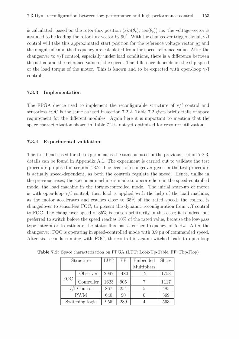
7.3 Dyn. reconfiguration between low-performance and high performance control 153
is calculated, based on the rotor-flux position (sin(θr), cos(θr)) i.e. the voltage-vector is
assumed to be leading the rotor-flux vector by 90
. With the changeover trigger signal, v/f
control will take this approximated start position for the reference voltage vector u∗s and
the magnitude and the frequency are calculated from the speed reference value. After the
changeover to v/f control, especially under load conditions, there is a difference between
the actual and the reference value of the speed. The difference depends on the slip speed
or the load torque of the motor. This is known and to be expected with open-loop v/f
control.
7.3.3 Implementation
The FPGA device used to implement the reconfigurable structure of v/f control and
sensorless FOC is the same as used in section 7.2.2. Table 7.2 gives brief details of space
requirement for the different modules. Again here it is important to mention that the
space characterization shown in Table 7.2 is not yet optimized for resource utilization.
7.3.4 Experimental validation
The test bench used for the experiment is the same as used in the previous section 7.2.3,
details can be found in Appendix A.1. The experiment is carried out to validate the test
procedure proposed in section 7.3.2. The event of changeover given in the test procedure
is actually speed-dependent, as both the controls regulate the speed. Hence, unlike in
the previous cases, the specimen machine is made to operate here in the speed-controlled
mode, the load machine in the torque-controlled mode. The initial start-up of motor
is with open-loop v/f control, then load is applied with the help of the load machine;
as the motor accelerates and reaches close to 35% of the rated speed, the control is
changedover to sensorless FOC, to present the dynamic reconfiguration from v/f control
to FOC. The changeover speed of 35% is chosen arbitrarily in this case; it is indeed not
preferred to switch before the speed reaches 10% of the rated value, because the low-pass
type integrator to estimate the stator-flux has a corner frequency of 5 Hz. After the
changeover, FOC is operating in speed-controlled mode with 0.9 pu of commanded speed.
After six seconds running with FOC, the control is again switched back to open-loop
Table 7.2: Space characterization on FPGA (LUT: Look-Up-Table, FF: Flip-Flop)
Structure LUT FF Embedded Slices
Multipliers
Observer 2997 1480 12 1753FOC
Controller 1623 905 7 1117
v/f Control 867 254 5 485
PWM 640 90 0 369
Switching logic 955 289 4 563
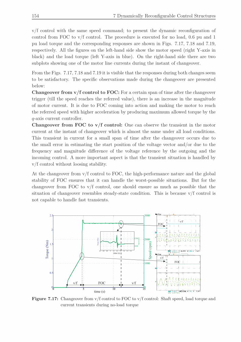
154 7 Dynamically Reconfigurable Control Structures
v/f control with the same speed command; to present the dynamic reconfiguration of
control from FOC to v/f control. The procedure is executed for no load, 0.6 pu and 1
pu load torque and the corresponding responses are shown in Figs. 7.17, 7.18 and 7.19,
respectively. All the figures on the left-hand side show the motor speed (right Y-axis in
black) and the load torque (left Y-axis in blue). On the right-hand side there are two
subplots showing one of the motor line currents during the instant of changeover.
From the Figs. 7.17, 7.18 and 7.19 it is visible that the responses during both changes seem
to be satisfactory. The specific observations made during the changeover are presented
below:
Changeover from v/f control to FOC: For a certain span of time after the changeover
trigger (till the speed reaches the referred value), there is an increase in the magnitude
of motor current. It is due to FOC coming into action and making the motor to reach
the referred speed with higher acceleration by producing maximum allowed torque by the
q-axis current controller.
Changeover from FOC to v/f control: One can observe the transient in the motor
current at the instant of changeover which is almost the same under all load conditions.
This transient in current for a small span of time after the changeover occurs due to
the small error in estimating the start position of the voltage vector and/or due to the
frequency and magnitude difference of the voltage reference by the outgoing and the
incoming control. A more important aspect is that the transient situation is handled by
v/f control without loosing stability.
At the changeover from v/f control to FOC, the high-performance nature and the global
stability of FOC ensures that it can handle the worst-possible situations. But for the
changeover from FOC to v/f control, one should ensure as much as possible that the
situation of changeover resembles steady-state condition. This is because v/f control is
not capable to handle fast transients.
0 5 10 150
0.5
1
1.5
2
2.5
Torq
ue
(Nm
)
time (s)0 5 10 15
0
1000
2000
3000
10.7 10.8 10.9 11 11.1 11.2 11.3 11.4 11.5 11.6
Torq
ue
(Nm
)
time (s)10.7 10.8 10.9 11 11.1 11.2 11.3 11.4 11.5 11.6
2650
2700
v/f v/f
v/f
FOC
v/fFOC
FOC
Sp
eed
(rp
m)
Sp
eed
(rp
m)
Figure 7.17: Changeover from v/f control to FOC to v/f control: Shaft speed, load torque and
current transients during no-load torque

7.4 Summary 155
0 5 10 150
0.5
1
1.5
2
2.5
To
rqu
e (N
m)
time (s)0 5 10 15
0
1000
2000
3000
FOCv/f v/f
v/f
FOC
v/fFOC
11.3 11.4 11.5 11.6 11.7 11.8 11.9 12 12.1
Torq
ue
(Nm
)
time (s)11.3 11.4 11.5 11.6 11.7 11.8 11.9 12 12.1
2600
2650
2700
Spee
d (
rpm
)
Spee
d (
rpm
)
Figure 7.18: Changeover from v/f control to FOC to v/f control: Shaft speed, load torque and
the current transients during 0.6 pu load torque
0 5 10 150
0.5
1
1.5
2
2.5
Torq
ue
(Nm
)
time (s)0 5 10 15
0
1000
2000
3000
10.3 10.4 10.5 10.6 10.7 10.8 10.9 11 11.1
To
rqu
e (N
m)
time (s)10.3 10.4 10.5 10.6 10.7 10.8 10.9 11 11.1
2550
2600
2650
FOCv/f v/f
v/f
FOC
v/fFOC
Spee
d (
rpm
)
Sp
eed
(rp
m)
Figure 7.19: Changeover from v/f control to FOC to v/f control: Shaft speed, load torque and
the current transients during 1 pu load torque
7.4 Summary
A detailed motivation for the novel concept “dynamically reconfigurable structure” is
defined. The general case of reconfigurable control based on popular control schemes is
outlined. The general case is demonstrated by considering two sets of control combinations
i.e. the reconfiguration between two high-performance controls and between a high- and
a low-performance control. These individual set of controls are dealt in-detail with an
induction-motor drive, which can be extended in general to any three-phase motor drive.
For the realization of these control structures, a control platform based on the Xilinx
Virtex-2P FPGA is utilized; details for the space characterization and the implementation
are given.

156 7 Dynamically Reconfigurable Control Structures
To validate the proposed concept, elaborate experiments have been carried out on a test
bench under different load conditions. The presented results show satisfactory operation
of the system in most of the worst operating conditions.
Controller-design based on FPGAs is getting more popular in industry and it is expected
to be employed in production lines in the very near future. From the course of investiga-
tions it is found that the dynamic changeover between the controls is very essential and
it is a appealing to offer this as an optional feature with standard drives from the manu-
facturer. Looking into the future, dynamic reconfiguration will be gaining importance in
the drive market.
157
8 Conclusions
This thesis deals with the application of generic FPGAs in electrical drive control. It starts
with finding areas in the drive control platform where the generic component capabilities
can be exploited. The main emphasis is laid on making the drive controller more simple,
robust and highly dynamic. The specific topics addressed in this thesis are:
• Application of Delta-Sigma ADCs for analog signal measurement.
• Design of well-known motor-control algorithms using a quasi-continuous approach.
• Reconfigurable structures for optimal performance and fault-tolerant control.
In all these topics the analysis and design is mostly based on a detailed analytical ap-
proach, followed by an experimental validation.
Implementing the control algorithms on a FPGA is still at a primitive level. There is
no fixed methodology for the algorithm development on these devices because of their
generic nature. Therefore design engineers have greater flexibility to develop strategies
for implementation. Chapter 3 presents and demonstrates that the multiplexed archi-
tecture can solve the issue of optimal usage of the limited resources on a FPGA. For
the demonstration a current controller is considered and its detailed implementation and
comparison are given.
An efficient data conversion using 1-bit Delta-Sigma modulators in the drive control is
presented in chapter 4. The motive behind is to make data acquisition more robust,
simple and superior. CIC-type and IIR-type filters are explored for the attenuation of
quantization noise of the modulator output. In the course of investigations to meet the re-
quirements with the CIC filter, it is demonstrated that only simple and fast compensation
techniques are viable. An efficient method based on the cascaded approach to overcome
the poor space utilization of the direct form of IIR realization is described. The exper-
imental comparison of time and frequency responses, noise power (SNR) and resolution
(ENOB) for both topologies concludes that the cascaded-type IIR filter performs better
in all these areas and is more efficient in terms of space and Slice utilization.
A novel quasi-continuous control based on FPGA realization is presented in chapter 5.
The analytical design procedure for the well-known FOC and ISC controls described
separately. The following important improvements in general for both the controls have
been achieved:
• The quasi-continuous approach demonstrates that the torque-controller bandwidth
can be improved considerably compared to the sampled controller; a range of 3:1 is
feasible. This is achieved without increasing the switching frequency of the inverter.

158 8 Conclusions
• The small delays in the current measurement in the range of few microseconds are
unavoidable due to practical constraints. The investigations clearly demonstrate
that for quasi-continuous PWM controllers these delays have negligible effect, and
further they can even be exploited to enhance the controller dynamics.
• The current distortion produced by the highly dynamic quasi-continuous control is
always within the best possible range of regular-sampled control.
In chapter 6, an approach is outlined to find adaptive hysteresis bands for DTC to ensure
a constant average switching frequency of the inverter throughout the operating region.
The selected combination of bands will ensure lowest THD in the motor line currents and
hence is defined as optimal. The presented procedure is completely offline and analytical.
With a FPGA being used for implementation, it is possible to approximate the control as
a continuous-time system. This simplifies the analytical calculations. The experimental
results match close the analytical values, but still there exists room for improvement. In
order to address the improvements, detailed suggestions are given for the data acquisition
system. As in this particular contribution only the constant-torque region of the PMSM
is considered, it will be valuable to continue the work for the field-weakening region. It
is also desirable to extend the work by generalizing the approach for any three-phase
machine.
The performance comparison of quasi-continuous PWM control and DTC shows that the
dynamic performance of DTC is still the best, while PWM controls set the benchmark for
THD performance. The same holds true for sampled controls, but with quasi-continuous
approach the gap between their performances is very narrow. There is very little margin
to discriminate them based on the performance.
In chapter 7, a detailed motivation for a “dynamically reconfigurable structure” is defined.
The general case of reconfigurable control based on the popular motor control schemes is
outlined. This general case is demonstrated by considering two sets of control combina-
tions, i.e. the reconfiguration between two high-performance controls and between a high-
and a low-performance control. These individual set of controls are dealt in-detail with an
induction motor; but this can be extended in general to any three-phase motor drive. To
validate the proposed concept, elaborate experiments have been carried out under differ-
ent load conditions. The results show the satisfactory operation under extreme operating
conditions. In this chapter the focus is not on the fault identification and isolation. It is
worthwhile to investigate these issues with the quasi-continuous approach, because timing
issues are very critical with FTC systems.
The investigations presented in this thesis prove the potential capabilities of FPGAs in the
field of electrical drives. As a trend, the controller design based on FPGAs is becoming
more and more popular in industries, and FPGA controllers are expected to be employed
in the production lines in the very near future.
159
Bibliography
[ABB-01] Technical guide no. 1–Direct Torque Control. Asian Brown Boveri (ABB)
application note (www.library.abb.com)
[ABB-02] ABB low and medium voltage drive–series ACS 800/850/1000/5000/6000.
Asian Brown Boveri (ABB) user manual (www.library.abb.com)
[AH1993] E. Ch. Andresen and A. Haun: Influence of the Pulse-Width Modulation
Control Method on the Performance of Frequency Inverter Induction Motor
Drives. ETEP vol. 3, 1993, pp. 151–161
[AN2007] Understanding CIC compensation filters. Altera application note 455-1.0
April 2007 (www.altera.com/literature/an/an455.pdf)
[AR2009] A. Ruderman: Understanding PWM current ripple in start-connected AC
motor drives. IEEE power electronics newsletter–15, 2nd quarter 2009, pp.
14–17
[AS1995] P.J. Ashenden: The designer’s guide to VHDL. Morgan Kaufmann, 1995,
ISBN 1-55860-270-4
[AS1996] M.P. Aziz, H.V. Sorensen and Van der Spiegel: An overview of Sigma-Delta
converters: How a 1-bit ADC achieves more than 16-bit resolution. IEEE
signal processing magazine, vol. 13, September 1996, pp 61–84
[AS2004] A. Steimel: Direct Self Control and synchronous pulse techniques for high-
power traction inverters in comparison. IEEE Transactions on Industrial
Electronics vol. 51, 2004, pp. 810–820
[AS2008] A. Steimel: Electric Traction–Motive Power and Energy Supply. Oldenbourg
Industrie Gmbh, 2008
[BC2001] B. D. Brown and H.C. Card: Stochastic neural computation I: Computational
elements. IEEE transactions on computers, vol. 50, September 2001, pp. 891–
905
[BK2004] G.S. Buja, M.P. Kazmierkowski: Direct torque control of PWM inverter-fed
AC motors - a survey. IEEE transactions on industrial electronics, vol. 51,
August 2004, pp. 744–757
[BP1997] S. Bennett, R. Patton and S. Daley: Using bilinear motor model for sensor
fault-tolerant rail traction drive. 3rd symposium on fault detection supervision
and safety for technical processes (IFAC SAFEPROCESS), 1997, pp. 783–788
[BP2002] K. Bondalapati and V.K. Prasanna: Reconfigurable computing systems. Pro-
ceedings of the IEEE, vol. 90, July 2002, pp. 1201–1217

160 BIBLIOGRAPHY
[BR1969] B.R. Gaines: Stochastic computing systems. Advances in information systems
science (Plenum press), vol. 2, 1969, pp. 37–172
[BS2006] J. Böcker, B. Schulz, T. Knoke and N. Fröhleke: Self-optimization as a frame-
work for advanced control systems. IEEE industrial electronics conference
(IECON), 2006, pp. 4672–4676
[BS1988] H.W. van der Broeck, H.C. Skudelny and G.V. Stanke: Analysis and re-
alization of a pulse width modulator based on voltage space vectors. IEEE
transactions on industry applications, vol. 24, Jan./Feb. 1988, pp. 142–150
[BV2010] J. Beerten, J. Verveckken and J. Driesen: Predictive direct torque control for
flux and torque ripple reduction. IEEE transactions on industrial electronics,
vol. 57, January 2010, pp. 404–412
[BW1988] B. Boser and B. Wooley: The design of sigma-delta modulation analog-to-
digital converters. IEEE Journal of Solid State Circuits, December 1988, pp.
1298–1308
[CG1994] D. Casadei, G. Grandi, G. Serra and A. Tani: Effects of flux and torque
hysteresis band amplitude in direct torque control of induction machines .
IEEE industrial electronics conference (IECON), 1994, pp. 299–304
[CM2004] C. Maxfield: The design warrior’s guide to FPGAs: Devices, tools and
flows. Elsevier’s science and technology ISBN 0-7506-7604-3
[CT1965] J.W. Cooley and J.W. Tukey: An algorithm for the machine calculation of
complex Fourier series. Mathematics of computation, vol. 19, April 1965, pp.
297–301
[CT1992] J. Candy and G. Temes: Oversampling methods for A/D and D/A conver-
sion. In: Oversampling delta-sigma converters IEEE press, 1992, pp. 1–25
[DE1988] M. Depenbrock: Direct self-control (DSC) of inverter-fed induction machine.
IEEE transactions on power electronics, vol. 3, July 1988, pp. 420–429
[DH2009] G.J. Dolecek and F. Harris: Design of wideband CIC compensator filter for a
digital IF receiver. Elsevier journal on digital signal processing, vol. 19, 2009,
pp. 827–837
[DM2008] G.J. Dolecek and S.K. Mitra: Simple method for compensation of CIC deci-
mation filters. Electronics letter, vol. 44, 2008, pp. 1162–1163
[DT2008] D.U.C. Delgado, D.R.E. Trejo and E. Palacios: Fault-tolerant control in vari-
able speed drives: a survey. IET electric power application 2008, pp. 121–134
[EH1981] E. Hogenauer: An economical class of digital filters for decimation and in-
terpolation. IEEE transactions on acoustics, speech and signal processing,
vol. 29, April 1981, pp. 155–162

BIBLIOGRAPHY 161
[EL2010] A.M. El-Refaie: Fractional-slot concentrated-windings synchronous perma-
nent magnet machines: Opportunities and challenges. IEEE transactions on
industrial electronics, vol. 57, 2010, pp. 107–121
[FB1972] F. Blaschke: The principles of field orientation as applied to the new
TRANSVEKTOR closed-loop control system for rotating field machines.
Siemens review, vol. 39, 1972, pp. 217–220
[GL1980] R. Gabriel, W. Leonhard and C.J. Nordby: Field-oriented control of a stan-
dard AC motor using microprocessor. IEEE transactions on industry appli-
cations, vol. 16, 1980, pp.186–192
[GP2009] T. Geyer, G. Papafotiou and M. Morari: Model predictive direct torque con-
trol part–I: Concept, algorithm and analysis. IEEE transactions on industrial
electronics, vol. 56, June 2009, pp. 1894–1905
[HB1973] H. Becker: Dynamisch hochwertige Drehzahlreglung einer umrichtergespeis-
ten Asynchronmaschine. Regelungstechnische Praxis und Prozessrechentech-
nik 1973
[HJ1995] F. Hoffmann and M. Jänecke: Fast torque control of an IGBT-inverter fed
three phase A.C. drive in the whole speed range - experimental result. 6th
EPE conference, 1995, pp. 3399–3404
[HL1979] H. Lam: Analog and digital filters: design and realizations. Prentice Hall
series ISBN 0-13-032755-7
[HO2004] T. Hestermeyer, O. Oberschelp and H. Giese: Structured information pro-
cessing for self-optimizing mechatronic systems. Procedings of 1st ICINCO,
August 2004, INSTICC Press, pp. 230–237
[HP1992] T.G. Habetler and F. Profumo: Direct torque control of induction machines
using space vector modulation. IEEE transactions on industry applications,
vol. 28, Sept./Oct. 1992, pp. 1045–1052
[IN2007] L. Idkhajine1, M.W. Naouar, E. Monmasson and A. Prata: Fully FPGA-
based system on chip solution for current control of AC machine. 12th EPE
conference, 2007, pp. 1–10
[JB2004] J. Böcker: Tolerance band controller for a three-level four-quadrant converter
including DC link balancing. 35th IEEE power electronics specialist confer-
ence (PESC), 2004, pp. 4238–4242
[JB2006] J. Böcker: Bitstream-Arithmetik. Internal and private communication at the
Institute of Power Electronics and Electrical Drives, University of Paderborn,
March 2006
162 BIBLIOGRAPHY
[JC1985] J. Candy: A use of double integration in sigma-delta modulation. IEEE
transactions on communications, vol. 33, March 1985, pp. 249–258
[JH2006] J. Holtz: Sensorless control of induction machines - with or without signal in-
jection?. IEEE transactions on industrial electronics, vol. 53, February 2006,
pp. 7–30
[JK1990] M. Jänecke, R. Kremer and G. Steuerwald: Direct self-control, a novel
method of controlling asynchronous machines in traction applications. Elek-
trische Bahnen 88 (1990), pp. 81–87
[JT1977] J.W. Tukey: Exploratory data analysis. Addison-Wesley, 1977, ISBN 0-201-
07616-0
[KH1969] K. Hasse: Zur Dynamik drehzahlgeregelter Antriebe mit stromrichtergespeis-
ten Asynchron-Kurzschlußläufermotoren. Ph.D. dissertation, Technical Uni-
versity of Darmstadt, 1969
[KH1977] J.F. Kaiser and R.M. Hamming: Sharpening the response of a symmetric
non-recursive filter by multiple use of the same filter. IEEE transactions on
acoustics, speech and signal processing, vol. 25, 1977 pp. 415–422
[KK1995] M. P. Kazmierkowski and A. B. Kasprowicz : Improved direct torque and flux
vector control of PWM inverter-fed induction motor drives. IEEE transac-
tions on industrial electronics, vol. 42, August 1995, pp. 344–350
[KL2006] S. Kim, W.S. Lee, S. Ahn and S. Choi: Design of CIC roll-off compensation
filter in a W-CDMA digital receiver. Digital signal processing-16, 2006, pp
846–854
[KS2001] J. K. Kang and S. K. Sul: Analysis and prediction of inverter switching
frequency in direct torque control of induction machine based on hysteresis
bands and machine parameters. IEEE transactions on industrial electronics,
vol. 48, June 2001, pp. 545–553
[KW1997] A. Kwentus and A. Willson Jr: Application of filter sharpening to cascaded
integrator-comb decimation filters. IEEE transactions on signal processing,
vol.45, February 1997, pp. 457–467
[LC1999] D.H. Lee, A. Choi, J.M. Koo, J.I. Lee and B.M. Kim: A wide-band DS-CDMA
modem for a mobile station. IEEE transactions on consumer electronics, vol.
45, November 1999, pp. 1259–1269
[LE1976] W. Leonhard: Introduction to control engineering and linear control systems
(translated from German). Springer-Verlag, 1976, ISBN 3-528-03017-8
[LE2001] W. Leonhard: Control of electric drives. Springer, 2001, ISBN 3-540-41820-
2

BIBLIOGRAPHY 163
[MB2007] S. Mathapati and J. Böcker: Implementation of dynamically reconfigurable
control structures on a single FPGA platform. 12th EPE Conference, 2007
[MB2010] S. Mathapati and J. Böcker: Dynamically reconfigurable control structure
for induction motor drives on FPGA control platform. EPE journal, vol. 20,
2010, pp. 21-32
[MC2007] E. Monmasson and M.N. Cirstea: FPGA design methodology for industrial
control systems–A review. IEEE transactions on industrial electronics, vol.
54, Aug. 2007, pp. 1824–1842
[MR2002] E. Monmasson, B. Robyns and E. Mendes: Dynamic reconfiguration of con-
trol and estimation algorithms for induction motor drives. Proceedings of
IEEE International Symposium on Industrial Electronics (ISIE), vol. 3, July
2002, pp. 828–833
[NP1989] S. Norsworthy, I. Post, and H. Fetterman: A 14-bit 80kHz sigma-delta AID
converter: modeling, design, and performance evaluation. IEEE journal of
solid state circuits, vol. 24, April 1989, pp. 256–266
[NR1993] S. Norsworthy and D. Rich: Idle channel tones and dithering in delta sigma
modulators. 95th convention of the audio engineering society, pre-print 3711,
October 1993
[NS1996] S. Norsworthy, R. Schreier and G. Temes: Delta-Sigma data converters: The-
ory, design and simulation. Wiley-IEEE press, October 1996, ISBN 978-0-
7803-1045-2
[NT1997] T. Noguchi and I. Takahashi: High frequency switching operation of PWM
inverter for direct torque control of induction motor. IEEE-IAS annual meet-
ing, 1997, pp. 775–780
[OV2004] S.J. Ovaska and O. Vainio: Evolutionary programming based optimization of
reduced-rank adaptive filters for reference generation in active power filters.
IEEE transactions on industrial electronics, vol. 51, August 2004, pp. 910–
916
[PA1996] S. Palnitkar: Verilog HDL: A guide to digital design and synthesis. Prentice-
Hall, 1996, ISBN 013-044911-3
[PD1995] P. Pirsch, N. Demassieux and W. Gehrke: VLSI architectures for video
compression–A survey. Proceedings of IEEE, vol. 83, February 1995, pp.
220–246
[RG1982] R. Gabriel: Feldorientierte Regelung einer Asynchronmaschine mit einem
Mikrorechner. Dissertation, Technical University of Braunschweig, 1982

164 BIBLIOGRAPHY
[RL1994] S. Rangan and B. Leung: Quantization noise spectrum of double-loop sigma-
delta converter with sinusoidal input. IEEE transactions on circuits and sys-
tems II, vol. 41, February 1994, pp. 168–173
[RP1997] R. Patton: Fault-tolerant control systems: the 1997 situation. 3rd sympo-
sium on fault detection supervision and safety for technical processes (IFAC
SAFEPROCESS), 1997, pp. 1033–1054
[RT1999] T. Riesgo, Y. Torroja and E. De la Torre: Design methodologies based on
hardware description languages. IEEE transactions on industrial electronics,
vol. 46, February 1999, pp. 3–12
[SFB614] SFB614: Collaborative research center 614, Self-optimizing concepts and
structures in mechanical engineering. http://www.sfb614.de/en/sfb614/
[SF2001] R.B. Sepe Jr, B. Fahimi and C. Morrison: Fault tolerant operation of induc-
tion motor drives with automatic controller reconfiguration. IEEE IEMDC
conference, 2001, pp. 156–162
[ST2004] R. Schreier and G. Temes: Understanding delta sigma data converters. Wiley-
IEEE press, October 2004, ISBN 0-471-46585-2
[TN1986] I. Takahashi and T. Noguchi: A new quick-response and high-efficiency con-
trol strategy of an induction motor. IEEE transactions on industry applica-
tions, vol. 22, Sept./Oct. 1986, pp. 820–827
[UB1989] U. Baader: Hochdynamische Drehmomentregelung einer Asynchronmaschine
im ständer-flußbezogenen Koordinatensystem. EtzArchiv-6, 1989, pp. 11–16
[UM2007] U. Meyer-Baese: Digital signal processing with field programmable gate ar-
rays. Springer, ISBN 978-3-540-72612-8
[VS1988] G.C. Verghese and S.R. Sanders: Observers for flux estimation in induction
machines. IEEE transactions on industrial electronics, vol. 35, February 1998,
pp. 85–94
[WB1948] W. Bennett: Spectra of quantized signals. Bell System Technical Journal,
July 1948, pp. 446–472
[WM1991] M. Weinhold: Appropriate pulse width modulation for a three-phase PWM
AC-to-DC converter. EPE-Journal vol. 1, 1991, pp. 139–148
[WZ1984] W. Zägelein: Drehzahlregelung des Asynchronmotors unter Verwendung
eines Beobachters mit geringer Parameterempfindlichkeit. Dissertation, Uni-
versity of Erlangen, 1984
[YC2004] K.S. Yeung and S.C. Chan: The design and multiplier-less realization of soft-
ware radio receivers with reduced system delay. IEEE transactions on circuits
and systems, vol. 51, 2004, pp. 2444–2459

BIBLIOGRAPHY 165
[YS2009] J.S. Yim, S.K. Sul, B.H. Bae, N.R. Patel and S. Hiti: Modified current control
schemes for high-performance permanent-magnet AC drives with low sam-
pling to operating frequency ratio. IEEE transactions on industry applica-
tions, vol. 45(2), 2009, pp. 763–771

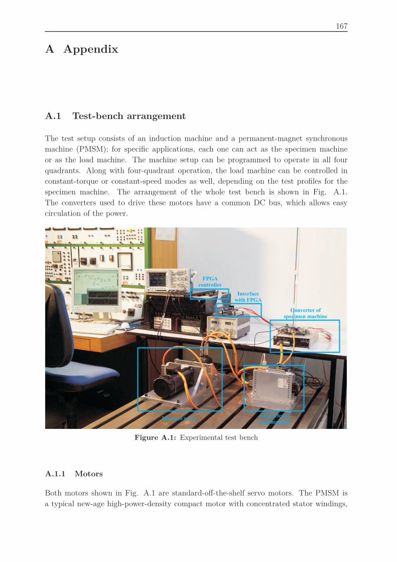
167
A Appendix
A.1 Test-bench arrangement
The test setup consists of an induction machine and a permanent-magnet synchronous
machine (PMSM); for specific applications, each one can act as the specimen machine
or as the load machine. The machine setup can be programmed to operate in all four
quadrants. Along with four-quadrant operation, the load machine can be controlled in
constant-torque or constant-speed modes as well, depending on the test profiles for the
specimen machine. The arrangement of the whole test bench is shown in Fig. A.1.
The converters used to drive these motors have a common DC bus, which allows easy
circulation of the power.
FPGAcontroller
Interfacewith FPGA
Converter ofspecimen machine
Converter ofload machine
Machine setup
Figure A.1: Experimental test bench
A.1.1 Motors
Both motors shown in Fig. A.1 are standard-off-the-shelf servo motors. The PMSM is
a typical new-age high-power-density compact motor with concentrated stator windings,
168 A Appendix
while the induction machine has standard distributed windings. Details of motor ratings
and parameters are given in table A.1. The PMSM has an optical encoder (ECN1313
from Heidenhain) for position measurement with inbuilt interface circuit. The output
signal has 13-bit resolution, represented in Gray code. The data is acquired by the FPGA
with a simple serial synchronous interface (SSI) protocol. The induction machine has
a resolver TS2620N21E11 from Tamagawa. The Analog Devices AD2S1200 resolver-to-
digital converter is used in-between before sending the position information to the FPGA.
The converted digital signal has 12 bit of resolution.
Table A.1: Motor ratings and parameters
Details PMSM Induction machine
(LSH-097-1-30-320/T1,G5) (ASM-12-10R23-000)
Voltage 190 V 190 V
Current 5 A 3.2 A
Ratings Frequency 250 Hz 104.4 Hz
Torque T 3.2 Nm 1.7 Nm
Speed n 3000 min−1 3000 min−1
Power P 1 kW 0.6 kW
Stator resistance Rs 0.62 Ω 1.75 Ω
Rotor resistance Rr - 1.56 Ω
Stator inductance Ls 5.3·10−3 H 76.2·10−3 H
Parameters Rotor inductance Lr - 76.2·10−3 H
Mutual inductance M - 72·10−3 H
Back EMF constant ke 0.0625 Vs−1 -
Number of pole pairs p 5 2
A.1.2 Converters and controllers
The converters used for the specimen and the load machine are different, as can be seen
in Fig. A.1. Depending on the test requirements, appropriate converters are connected
to the motors. Table A.2 give a short overview of the converters and controllers used
for the specimen and the load. The controller for the load machine is integrated into
Table A.2: Details of converters and controllers
Specimen machine Load machine
Converter ServoOne (LTi DRiVES) CDD3000 (LTi DRiVES)
Controller FPGA-based RAPTOR2000 GUI-based CDD Controller
the CDD3000 converter. The GUI-based application is used to generate the control pro-
files in terms of speed and torque references. The converter is connected to the hostPC
using a RS232 serial interface. The specimen motor controller is RAPTOR2000. It is
a modular FPGA-based rapid-prototyping system of the RAPTOR family, it integrates

A.2 Estimation of THD in DTC 169
all key components to realize the circuit and system design with very high complexity.
It allows to install as many as six modular FPGA boards on this platform; the Vertex
II Pro XC2VP20 and XC2VP30 modules are used for most implementations. RAPTOR
supports the acceleration of computationally intensive applications as well as the par-
tial dynamic reconfiguration, further details on this modular system can be found at
http://www.raptor2000.de/en/sct/extern/raptor2000/.
A.2 Estimation of THD in DTC
To evaluate the THD of the motor line currents analytically, it is necessary at first to find
the instantaneous current ripple. The current vector can be represented as components
in different coordinates as in (A.1).
ixys = isx + jisy
idqs = isd + jisq(A.1)
where x/y and d/q correspond to stator-flux and rotor-flux coordinates, respectively. In
steady-state operation the individual current components are evaluated for one particular
sector. That will be enough to evaluate the THD, because the trajectory is simply the
repetition for the other sectors. To evaluate the ripple current in the vector components
in (A.1), either of these coordinates can be used. However, as the procedure used in
chapter 6 is using d/q coordinates for the evaluation of the torque-controller and the
flux-controller frequency, the same is used here as well.
Let us consider sector1 in Fig. 6.2, wherein v2 and v3 are the used active vectors. In order
to calculate the instantaneous values of the current components it is essential to know
the applied voltages in the respective directions. (A.2) gives the applied d- and q-axis
voltages due to the active vectors v2 and v3 and the zero vector.
uq(v2) =2udc
3cos(θs − δT +
π
6)
uq(v3) =2udc
3cos(θs − δT −
π
6)
ud(v2) =2udc
3sin(θs − δT +
π
6)
ud(v3) =2udc
3sin(θs − δT −
π
6)
ud(v0/v7) = uq(v0/v7) = 0
(A.2)
With the help of the d- and q-axis voltages evaluated in (A.2), the respective instantaneous
current components can be evaluated as in (A.3).
isd =1
Ls
∫
[ud(v2,v3,v0,v7) −Rsisd + ωLsisq] dt
isq =1
Ls
∫
[uq(v2,v3,v0,v7) − Rsisq − ω(Lsisd + ψp)] dt(A.3)
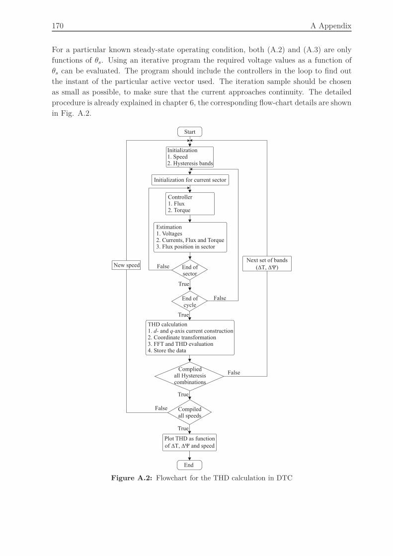
170 A Appendix
For a particular known steady-state operating condition, both (A.2) and (A.3) are only
functions of θs. Using an iterative program the required voltage values as a function of
θs can be evaluated. The program should include the controllers in the loop to find out
the instant of the particular active vector used. The iteration sample should be chosen
as small as possible, to make sure that the current approaches continuity. The detailed
procedure is already explained in chapter 6, the corresponding flow-chart details are shown
in Fig. A.2.
End ofsector
Start
Initialization1. Speed2. Hysteresis bands
Estimation1. Voltages2. Currents, Flux and Torque3. Flux position in sector
Initialization for current sector
End ofcycle
False
False
True
THD calculation1. and axis current construction2. Coordinate transformation3. FFT and THD evaluation4. Store the data
d- q-
End
Compiledall speeds
Compliedall Hysteresiscombinations
True
Next set of bands
( )DT, DY
False
True
Controller1. Flux2. Torque
New speed
False
True
Plot THD as function
of DT, DY and speed
Figure A.2: Flowchart for the THD calculation in DTC