FPGA Acceleration of Multifunction Printer Image ... · S. Kannan is with HCL Technologies Limited...
11
WP-01223-1.0 1 Abstract— OpenCL adoption in the High Performance Computing, entertainment and scientific computing markets continues to grow. The flexibility and portability of OpenCL make it an excellent platform upon which to develop image processing applications. However, OpenCL has not yet been applied to the hardcopy printer and Multi-Function Printer, MFP, markets. The printer/MFP markets traditionally use full custom System On Chip, SOC, or ASIC, Application Specific Integrated Circuits, to perform image processing. In this paper we explore the application of OpenCL, in concert with an Altera SOC FPGA, Field Programmable Gate Array, to the core MFP image processing pipeline. The core image processing pipeline operates at a sustained rate of greater than 90 letter-sized pages per minute for a full color RGB, 600DPI, Dots Per Inch, image while simultaneously fitting in a cost effective FPGA device. The OpenCL pipeline provides at least 40x performance improvement compared to a C-based software pipeline running on an embedded CPU and a 5x improvement running on a high end desktop CPU. Index Terms—Application Specific Integrated Circuits, Field Programmable Gate Arrays, ASIC, FPGA, OpenCL, Image Processing Pipeline, Open Computing Language, Multi-function Printer, System On Chip. I. INTRODUCTION ISTORICALLY MFP and Printer vendors have developed custom ASIC or SOC devices to perform image processing operations. These ASIC/SOC devices include image pipelines that accept RGB data from CCD or CIS sensors and perform filtering, reduction/enlargement, Color Space Transformation, image segmentation and halftoning operations. The resulting processed image is then printed using subtractive colorants: – cyan; magenta; yellow; black. The goal is to accurately reproduce the original document on a printed copy without introducing visual artifacts. ASIC/SOC devices typically have a limited lifetime of three years before the underlying technologies, such as DDR memory and USB connectivity, become outdated. The investment required to develop a custom ASIC/SOC continues to increase as silicon technologies continue to shrink. A 28nm SOC with dual core processor, requisite connectivity, DDR3 memory controller, image processing, GPU, LCD controller, etc. can T. M. Hunter is with HCL America, Rochester Delivery Center, Rochester, NY 14580 USA (e-mail: [email protected]). D. Denisenko is with Altera Corporation, Toronto Technology Center, Toronto Ontario, CANADA, (e-mail:[email protected]). S. Kannan is with HCL Technologies Limited , Bangalore, INDIA, (e-mail: [email protected]). cost in excess of $10M to design, develop and deliver. Development cycles for large SOC/ASIC device are anywhere from 18-30 months depending on many factors including the amount and size of new IP, ability to leverage previous designs, design team experience and maturity of the targeted silicon technology. Product cycles in the printer/MFP market are anywhere from 24 to 36 months. The printer/MFP market growth rate is flat increasing the competitive pressure to deliver more functionality at a lower cost and with a shorter development cycle [1]. With ASIC/SOC development cycles approaching the same timeframe as an MFP product lifecycle, MFP/printer vendors need a new platform to enable shorter development and deployment cycles. The combination of OpenCL and FPGA based SOCs provide an intriguing solution to this dilemma. II. MFP IMAGE PROCESSING PIPELINE BACKGROUND A significant body of research has accumulated over the past 20 years in the area of document image processing [2][3]. The majority of early work was focused on image processing basics including calibrating input sensor data to provide uniform color, filtering to remove noise from sensors, scaling algorithms to allow image size reduction or magnification and halftoning to enable continuous tone image data to be printed using binary pixels. Current document image processing research and development is in the area of image analysis, content extraction and data compression technologies.[4][5][6] All MFP document image processing products perform a set of basic functions - copy, scan and print. Fig. 1 graphically illustrates the basic functions or pipelines in an MFP device. Copy and scan operations are similar and begin with conversion of raw RGB data from a scanning device to a device independent color space. The copy operation further processes the device independent color space image and creates a CMYK image for printing. The scan operation performs a different set of image processing operations on the device independent color space image. These operations may include image analysis, partitioning of the image P. Thippabathini is with HCL Technologies Limited , Bangalore, INDIA, (e- mail:[email protected]). J. M. Bold is with HCL America, Rochester Delivery Center, Rochester, NY 14580 USA (e-mail: [email protected]). P. Dusel is with HCL America, Rochester Delivery Center, Rochester, NY 14580 USA (e-mail: [email protected]). FPGA Acceleration of Multifunction Printer Image Processing using OpenCL Timothy M. Hunter, Member, IEEE, Dmitry Denisenko, Member, IEEE, Sarnath Kannan, Jared M. Bold, Student Member, IEEE, Prasanthi Thippabathini, and Peter Dusel P.E. H
Transcript of FPGA Acceleration of Multifunction Printer Image ... · S. Kannan is with HCL Technologies Limited...

WP-01223-1.0 1
Abstract— OpenCL adoption in the High Performance
Computing, entertainment and scientific computing markets
continues to grow. The flexibility and portability of OpenCL make
it an excellent platform upon which to develop image processing
applications. However, OpenCL has not yet been applied to the
hardcopy printer and Multi-Function Printer, MFP, markets. The
printer/MFP markets traditionally use full custom System On
Chip, SOC, or ASIC, Application Specific Integrated Circuits, to
perform image processing. In this paper we explore the application
of OpenCL, in concert with an Altera SOC FPGA, Field
Programmable Gate Array, to the core MFP image processing
pipeline. The core image processing pipeline operates at a
sustained rate of greater than 90 letter-sized pages per minute for
a full color RGB, 600DPI, Dots Per Inch, image while
simultaneously fitting in a cost effective FPGA device. The
OpenCL pipeline provides at least 40x performance improvement
compared to a C-based software pipeline running on an embedded
CPU and a 5x improvement running on a high end desktop CPU.
Index Terms—Application Specific Integrated Circuits, Field
Programmable Gate Arrays, ASIC, FPGA, OpenCL, Image
Processing Pipeline, Open Computing Language, Multi-function
Printer, System On Chip.
I. INTRODUCTION
ISTORICALLY MFP and Printer vendors have developed
custom ASIC or SOC devices to perform image processing
operations. These ASIC/SOC devices include image pipelines
that accept RGB data from CCD or CIS sensors and perform
filtering, reduction/enlargement, Color Space Transformation,
image segmentation and halftoning operations. The resulting
processed image is then printed using subtractive colorants: –
cyan; magenta; yellow; black. The goal is to accurately
reproduce the original document on a printed copy without
introducing visual artifacts.
ASIC/SOC devices typically have a limited lifetime of three
years before the underlying technologies, such as DDR memory
and USB connectivity, become outdated. The investment
required to develop a custom ASIC/SOC continues to increase
as silicon technologies continue to shrink. A 28nm SOC with
dual core processor, requisite connectivity, DDR3 memory
controller, image processing, GPU, LCD controller, etc. can
T. M. Hunter is with HCL America, Rochester Delivery Center, Rochester,
NY 14580 USA (e-mail: [email protected]). D. Denisenko is with Altera Corporation, Toronto Technology Center,
Toronto Ontario, CANADA, (e-mail:[email protected]).
S. Kannan is with HCL Technologies Limited , Bangalore, INDIA, (e-mail: [email protected]).
cost in excess of $10M to design, develop and deliver.
Development cycles for large SOC/ASIC device are
anywhere from 18-30 months depending on many factors
including the amount and size of new IP, ability to leverage
previous designs, design team experience and maturity of the
targeted silicon technology.
Product cycles in the printer/MFP market are anywhere from
24 to 36 months. The printer/MFP market growth rate is flat
increasing the competitive pressure to deliver more
functionality at a lower cost and with a shorter development
cycle [1].
With ASIC/SOC development cycles approaching the same
timeframe as an MFP product lifecycle, MFP/printer vendors
need a new platform to enable shorter development and
deployment cycles. The combination of OpenCL and FPGA
based SOCs provide an intriguing solution to this dilemma.
II. MFP IMAGE PROCESSING PIPELINE BACKGROUND
A significant body of research has accumulated over the past
20 years in the area of document image processing [2][3]. The
majority of early work was focused on image processing basics
including calibrating input sensor data to provide uniform color,
filtering to remove noise from sensors, scaling algorithms to
allow image size reduction or magnification and halftoning to
enable continuous tone image data to be printed using binary
pixels. Current document image processing research and
development is in the area of image analysis, content extraction
and data compression technologies.[4][5][6]
All MFP document image processing products perform a set
of basic functions - copy, scan and print. Fig. 1 graphically
illustrates the basic functions or pipelines in an MFP device.
Copy and scan operations are similar and begin with conversion
of raw RGB data from a scanning device to a device
independent color space. The copy operation further processes
the device independent color space image and creates a CMYK
image for printing. The scan operation performs a different set
of image processing operations on the device independent color
space image. These operations may include image analysis,
partitioning of the image
P. Thippabathini is with HCL Technologies Limited , Bangalore, INDIA, (e-
mail:[email protected]). J. M. Bold is with HCL America, Rochester Delivery Center, Rochester, NY
14580 USA (e-mail: [email protected]).
P. Dusel is with HCL America, Rochester Delivery Center, Rochester, NY 14580 USA (e-mail: [email protected]).
FPGA Acceleration of Multifunction Printer
Image Processing using OpenCL
Timothy M. Hunter, Member, IEEE, Dmitry Denisenko, Member, IEEE, Sarnath Kannan, Jared M. Bold,
Student Member, IEEE, Prasanthi Thippabathini, and Peter Dusel P.E.
H
WP-01223-1.0 2
Fig. 1 Simplified MFP Image Processing Pipeline
into multiple image planes with different frequency content,
OCR, Optical Character Recognition and data compression.
The resulting image or images are then transferred to either a
local storage media such as a USB flash drive or a network
device.
The Print function receives a document encoded in a PDL,
Page Description Language, or Graphics Display Interface
format. In the case of a PDL document the MFP device must
first interpret the document language and create a list of
primitive objects. The renderer takes these objects and
translates them into a digital CMYK bitmap/bytemap image.
The resulting digital image may be further processed and
optionally compressed. A GDI printer does not require the
interpreting process as the image is transferred to the printer as
a list of display objects.
Once the Print or Copy pipelines have created the CMYK
bitmap/bytemap image, the image(s) are sent to the engine for
printing on the desired media.
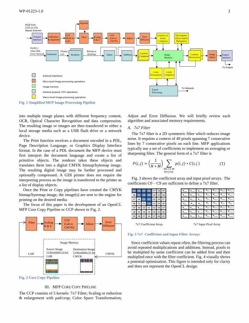
The focus of this paper is the development of an OpenCL
MFP Core Copy Pipeline or CCP shown in Fig. 2.
Fig. 2 Core Copy Pipeline
III. MFP CORE COPY PIPELINE
The CCP consists of 5 kernels: 7x7 Filter; Scaling or reduction
& enlargement with pad/crop; Color Space Transformation;
Adjust and Error Diffusion. We will briefly review each
algorithm and associated memory requirements.
A. 7x7 Filter
The 7x7 filter is a 2D symmetric filter which reduces image
noise. It requires a context of 49 pixels spanning 7 consecutive
lines by 7 consecutive pixels on each line. MFP applications
typically use a set of coefficients to implement an averaging or
sharpening filter. The general form of a 7x7 filter is
𝑃(𝑖, 𝑗) = (1
𝑁 ∗ 𝑀) ∑ 𝑝(𝑖, 𝑗)
0≤ 𝑖 ≤ 𝑚0<𝑗<𝑛
∗ 𝐶(i, j ) (1)
Fig. 3 shows the coefficient array and input pixel arrays. The
coefficients C0 – C9 are sufficient to define a 7x7 filter.
Fig. 3 7x7 Coefficient and Input Filter Arrays
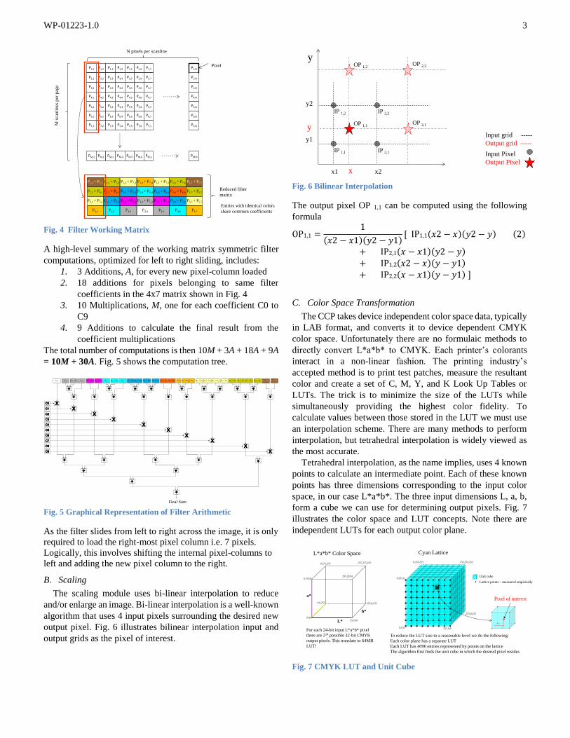
Since coefficient values repeat often, the filtering process can
avoid repeated multiplications and additions. Instead, pixels to
be multiplied by same coefficient can be added first and then
multiplied once with the filter coefficient. Fig. 4 visually shows
a potential optimization. This figure is intended only for clarity
and does not represent the OpenCL design.
Lossless
DecompressLossless
Compress
Interpreter
PS/PCL/
Other PDL
From NetworkDisplay
List Renderer
Bitmap or
Bytemap Adjust Lossless
DecompressEngine
Interface
Calibration
& alignment
CST
(RGB to
Lab)
Filter Scaling
R & EAdjust
CST
(Lab to
CMYK)
Lossless or
Lossy
Compress
Error
Diffusion
RGB from
CCD or CIS
Based Scanner
Segment
Image
Memory
Halftone
Decompress
Adjust and/or
Manipulate
Image memory
General purpose CPU operations
Macro-level Image processing operations
Micro-level Image processing operations
Export
Processing
Lossy
Decompress
Lossy
Compress
To Engine
To Network
Scanner
Interface
External interfaces
Image
Adjust
Lossless
Compress
LAB
Filter Scaling
R & EAdjust
CST
(Lab to
CMYK)
Error
Diffusion
Image Memory
Source Image
5100x6600x24-bit
LAB
Destination Image
5100x6600x32-bit
CMYKCMYK
C9 C8 C7 C6 C7 C8 C9
C8 C5 C4 C3 C4 C5 C8
C7 C4 C2 C1 C2 C4 C7
C6 C3 C1 C0 C1 C3 C6
C7 C4 C2 C1 C2 C4 C7
C8 C5 C4 C3 C4 C5 C8
C9 C8 C7 C6 C7 C8 C9
P(i-3,j-3) P(i-2,j-3) P(i-1,j-3)P(i,j-3) P(i+1,j-3) P(i+2,j-3) P(i+3,j-3)
P(i-3,j-2) P(i-2,j-2) P(i-1,j-2)P(i,j-2) P(i+1,j-2) P(i+2,j-2) P(i+3,j-2)
P(i-3,j-1) P(i-2,j-1) P(i-1,j-1)P(i,j-1) P(i+1,j-1) P(i+2,j-1) P(i+3,j-1)
P(i-3,j) P(i-2,j) P(i-1,j)P(i,j) P(i+1,j) P(i+2,j) P(i+3,j)
P(i-3,j+1) P(i-2,j+1) P(i-1,j+1)P(i,j+1) P(i+1,j+1) P(i+2,j+1) P(i+3,j+1)
P(i-3,j+2) P(i-2,j+2) P(i-1,j+2)P(i,j+2) P(i+1,j+2) P(i+2,j+2) P(i+3,j+2)
P(i-3,j+3) P(i-2,j+3) P(i-1,j+3)P(i,j+3) P(i+1,j+3) P(i+2,j+3) P(i+3,j+3)
7x7 Coefficient Array 7x7 Input Pixel Array
WP-01223-1.0 3
Fig. 4 Filter Working Matrix
A high-level summary of the working matrix symmetric filter
computations, optimized for left to right sliding, includes:
1. 3 Additions, A, for every new pixel-column loaded
2. 18 additions for pixels belonging to same filter
coefficients in the 4x7 matrix shown in Fig. 4
3. 10 Multiplications, M, one for each coefficient C0 to
C9
4. 9 Additions to calculate the final result from the
coefficient multiplications
The total number of computations is then 10M + 3A + 18A + 9A
= 10M + 30A. Fig. 5 shows the computation tree.
Fig. 5 Graphical Representation of Filter Arithmetic
As the filter slides from left to right across the image, it is only
required to load the right-most pixel column i.e. 7 pixels.
Logically, this involves shifting the internal pixel-columns to
left and adding the new pixel column to the right.
B. Scaling
The scaling module uses bi-linear interpolation to reduce
and/or enlarge an image. Bi-linear interpolation is a well-known
algorithm that uses 4 input pixels surrounding the desired new
output pixel. Fig. 6 illustrates bilinear interpolation input and
output grids as the pixel of interest.
Fig. 6 Bilinear Interpolation
The output pixel OP 1,1 can be computed using the following
formula
OP1,1 =1
(𝑥2 − 𝑥1)(𝑦2 − 𝑦1)[ IP1,1(𝑥2 − 𝑥)(𝑦2 − 𝑦) (2)
+ IP2,1(𝑥 − 𝑥1)(𝑦2 − 𝑦)
+ IP1,2(𝑥2 − 𝑥)(𝑦 − 𝑦1)
+ IP2,2(𝑥 − 𝑥1)(𝑦 − 𝑦1) ]
C. Color Space Transformation
The CCP takes device independent color space data, typically
in LAB format, and converts it to device dependent CMYK
color space. Unfortunately there are no formulaic methods to
directly convert L*a*b* to CMYK. Each printer’s colorants
interact in a non-linear fashion. The printing industry’s
accepted method is to print test patches, measure the resultant
color and create a set of C, M, Y, and K Look Up Tables or
LUTs. The trick is to minimize the size of the LUTs while
simultaneously providing the highest color fidelity. To
calculate values between those stored in the LUT we must use
an interpolation scheme. There are many methods to perform
interpolation, but tetrahedral interpolation is widely viewed as
the most accurate.
Tetrahedral interpolation, as the name implies, uses 4 known
points to calculate an intermediate point. Each of these known
points has three dimensions corresponding to the input color
space, in our case L*a*b*. The three input dimensions L, a, b,
form a cube we can use for determining output pixels. Fig. 7
illustrates the color space and LUT concepts. Note there are
independent LUTs for each output color plane.
Fig. 7 CMYK LUT and Unit Cube
P1,1
P2,1
P3,1
P4,1
P5,1
P6,1
P7,1
P1,2
P2,2
P3,2
P4,2
P5,2
P6,2
P7,2
P1,3
P2,3
P3,3
P4,3
P5,3
P6,3
P7,3
P1,4
P2,4
P3,4
P4,4
P5,4
P6,4
P7,4
P1,5
P2,5
P3,5
P4,5
P5,5
P6,5
P7,5
P1,6
P2,6
P3,6
P4,6
P5,6
P6,6
P7,6
P1,7
P2,7
P3,7
P4,7
P5,7
P6,7
P7,1
P1,N
P2,N
P3,N
P4,N
P5,N
P6,N
P7,N
N pixels per scanline
Pixel
Msc
anli
nes
per
pag
e
PM,1 PM,2 PM,3 PM,4 PM,5 PM,6 PM,1 PM,N
P1,1 + P7,1
P2,1 + P6,1
P3,1 + P5,1
P4,1
P1,2 + P7,2
P2,2 + P6,2
P3,2 + P5,2
P4,2
P1,3 + P7,3
P2,3 + P6,3
P3,3 + P5,3
P4,3
P1,4 + P7,4
P2,4 + P6,4
P3,4 + P5,4
P4,4
P1,5 + P7,5
P2,5 + P6,5
P3,5 + P5,5
P4,5
P1,6 + P7,6
P2,6 + P6,6
P3,6 + P5,6
P4,6
P1,7 + P7,7
P2,7 + P6,7
P3,7 + P5,7
P4,7
Reduced filter
matrix
Entries with identical colors
share common coefficients
+
P1,1 + P7,1P2,1 + P6,1P3,1 + P5,1P4,1 P1,2 + P7,2P2,2 + P6,2P3,2 + P5,2P4,2 P1,3 + P7,3P2,3 + P6,3P3,3 + P5,3P4,3 P1,4 + P7,4P2,4 + P6,4P3,4 + P5,4P4,4 P1,5 + P7,5P2,5 + P6,5P3,5 + P5,5P4,5 P1,6 + P7,6P2,6 + P6,6P3,6 + P5,6P4,6 P1,7 + P7,7P2,7 + P6,7P3,7 + P5,7P4,7
+ +
+
+
+
+ +
++
+ +
+
+
++
+
+
X
XC0
C1
XC2
XC3
XC4
XC5
XC6
XC7
XC8
XC9
+ + + + +
+ +
+
+
Final Sum
x
y
y2
y1
x1 x2
Input grid -----
Output grid -----
Input Pixel
Output Pixel
y
IP 1,1
IP 1,2
IP 2,1
IP 2,2
OP 1,1OP 2,1
OP 1,2OP 2,2
0,0,0255,0,0
0,255,0
255,0,255
255,255,255
0,0,255
0,255,255
L*
a*
b*
255,255,0
L*a*b* Color Space
0,0,0 255,0,0
0,255,0
255,0,255
255,255,2550,255,255
Cyan Lattice
For each 24-bit input L*a*b* pixel
there are 224 possible 32-bit CMYK
output pixels. This translate to 64MB
LUT!
To reduce the LUT size to a reasonable level we do the following:
Each color plane has a separate LUT
Each LUT has 4096 entries represented by points on the lattice
The algorithm first finds the unit cube in which the desired pixel resides
Pixel of interest
Lattice points – measured empirically
Unit cube

WP-01223-1.0 4
Once the algorithm has determined which unit cube contains
the output pixel of interest we must calculate the output pixel
from the set of 8 known pixels. This would be the case with Tri-
linear interpolation. Tetrahedral interpolation leverages the fact
that a unit cube can be partitioned into a set of 6 non-
overlapping tetrahedrons each of whose end-points are located
at unit cube vertices. Using a tetrahedron (with 4 points) to
interpolate cuts in half the number of pixels we must use to
interpolate a result. Fig. 8 graphically illustrates the six
tetrahedrons.
Fig. 8 CST Tetrahedrons
The CST algorithm first determines which tetrahedron the
output pixel, P, resides in and uses the 4 known output pixels to
interpolate the final result – see Fig. 7. Fig. 9 illustrates a pixel
P in tetrahedron 5. The algorithm calculates the distance
between each unit cube axis vertices and the pixel, dx, dy, dz
and uses the distance to linearly interpolate between known
points.
Fig. 9 CST Tetrahedron 5 Exploded View
D. TRC Adjust
The TRC Adjust algorithm is a straightforward LUT. It
allows further adjustment of the C, M, Y, K values to correct
for non-linear tone reproduction. The individual C, M, Y, K
LUT entries are measured empirically.
E. Error Diffusion
The final stage performs the halftoning function. Color laser
MFP products use a laser system to erase an electric charge on
a photoreceptor medium. Wherever charge is erased C, M, Y,
K toner cannot be transferred to the photoreceptor. The laser
beam sweeps across a moving photoreceptor and is modulated
to create an inverted image. The smallest time period of
modulation is a pixel. After the inverted image is written on the
photoreceptor it passes near a toner dispenser. The toner,
electrically charged to an opposite charge, is then attracted to
areas on the photoreceptor where a charge exists. The toner
“sticks” to the photoreceptor. The last step is to transfer the
image on the photoreceptor to the paper or other media.
Individual pixels are either on or off making the process a
binary one. The 8-bit CMYK pixels coming from the TRC
kernel must be halftoned or binarized in order to drive the laser
system in a printer. There are many algorithms to convert
continuous tone data to binary data. Error diffusion is a
common algorithm used in MFP/printers. We chose to
implement a variant of the well-known Floyd Steinberg error
diffusion algorithm with modified coefficients for arithmetic
simplicity [7].
Floyd-Steinberg error diffusion quantizes an input pixel based
on a threshold array and then distributes the residual error to
neighboring pixels. In our case we reduce an 8-bit input pixel
to a binary output pixel. Hence our threshold array is a single
value of 127. Input pixels greater than 127 become logic 1.
Pixels ≤ 127 become 0. The algorithm is defined as follows:
𝐼𝑃𝑡𝑒𝑚𝑝 = 𝐼𝑃(𝑥,𝑦) +1
2∗ 𝐸𝑃𝑃 +
1
4∗ 𝐸𝑃(x-1) +
1
8∗ 𝐸𝑃(x) +
1
16∗ 𝐸𝑃(x+1) +
1
32∗ 𝐸𝑃(x+2) +
1
32∗ 𝐸𝑃(x+3) (3)
𝐸𝑃(𝑥) = 𝐼𝑃𝑡𝑒𝑚𝑝 − 𝑞𝑢𝑎𝑛𝑡𝑖𝑧𝑒𝑑(𝐼𝑃𝑡𝑒𝑚𝑝) (4)
𝑂𝑃(x,y) = {1, 𝐼𝑃𝑡𝑒𝑚𝑝 > 𝑇ℎ𝑟𝑒𝑠ℎ𝑜𝑙𝑑
0, 𝐼𝑃𝑡𝑒𝑚𝑝 ≤ 𝑇ℎ𝑟𝑒𝑠ℎ𝑜𝑙𝑑 (5)
1. IP(x,y) is the current Input Pixel
2. EPP is the residual threshold error from the previous
pixel, IP(x-1,y)
3. EP is the error vector from the previous scanline, y-1.
IV. ALTERA OPENCL COMPILER
The most critical part of the OpenCL system beyond the actual
OpenCL code is the compiler. Altera SDK for OpenCL 13.1
provides a number of unique features including [8]:
A. Channels
B. I/O Channels
C. Memory access coalescing
D. Automatic loop pipelining
E. Shift register inference
A. Channels
The standard OpenCL model assumes kernels operate on
datasets based in global memory. An input chunk is read from
global memory by kernel #1, processed and the results are
Tetrahedron 1 Tetrahedron 2 Tetrahedron 3
Tetrahedron 4Tetrahedron 5
Tetrahedron 6
Tetrahedron 5
192,208,128
dy
dx dz
208,224,144
208,224,128
192,224,128
P
WP-01223-1.0 5
written back to a different portion of global memory. If a second
kernel needs to further process the results from kernel #1, it
must wait until kernel #1 is complete and all output data
is written back into global memory. Only then can kernel #2
read and process the data. Obviously this serial process results
in pipeline delays that increase at best linearly with each
additional kernel. Further every trip to and from memory
increases the Global memory bandwidth and reduces pipeline
throughput. To address this problem Altera has made available
the concept of kernel channels which allow the output results
from kernel #1 to go directly to the input of kernel #2. The
Altera Offline Compile, AOC, adds all the necessary
synchronization logic and FIFO memories to allow data to pass
from kernel n to kernel n+1. Fig. 10 shows the standard
OpenCL and Altera vendor extended Channels dataflow.
Fig. 10 OpenCL Dataflow with Altera's Channels Extension
B. IO Channels
IO channels are an extension to the channels concept that
allow external IO to connect directly to OpenCL kernels. IO
channels allow external ports such as Ethernet, serial LVDS or
an OEM proprietary interface to connect to a kernel(s) without
going into global memory first.
In our MFP example an IO Channel could allow RGB
scanner data to feed a calibration kernel and then connect to
the CCP. Additionally the CCP error diffused output video
data could feed an engine kernel that prints the image data on
a color printer. (Note we have not yet implemented IO
channels. This is reserved for future work.) Fig. 11 illustrates
the IO channels dataflow.
Fig. 11 OpenCL Dataflow with Altera Direct IO Channels
Extension
C. Memory Access Coalescence
DDR memory is very inefficient for random accesses. It is
best for long bursts of sequential data. Altera’s OpenCL
compiler provides both static and dynamic memory coalescing.
The compiler tries to statically identify multiple consecutive
requests in the OpenCL kernel code and creates hardware to
issue a single wide request. For example, if an array of integers
is accessed consecutively, the compiler will create hardware to
fetch eight integers at a time with a single request to DDR
controller. Furthermore, Altera’s OpenCL memory system
provides dynamic data reordering. The DDR input queue
accepts memory access request from various kernels in the
order they were received. An internal data reordering module
inspects the input queue addresses and operation type and then
dynamically reorders the requests. The reorder requests are
stored in a reorder buffer with optimized sequencing. The
memory controller reads from the reorder buffer and
stores/retrieves data in an optimized form. Fig. 12 shows the
high level DDR controller with reorder buffer.
Fig. 12 Altera DDR Controller Reordering
D. Automatic Loop Pipelining- ALP
OpenCL kernels usually describe the work of a single thread
with the intent of launching a large number of such threads to
process a single data set. However, some problems are best
expressed as single-threaded algorithms. Filtering and Error
Diffusion are two such examples. Using multiple threads to do
filtering would require either excessive memory reads, as will
be discussed later, or excessive communication among threads.
The Floyd Steinberg Error Diffusion algorithm, used in the
CCP, is very difficult to parallelize due to error propagation
from the current pixel to its neighbors.
Host CPU
Core 1 Core N
System Memory
Global
Memory
DDR3
Kernel NKernel
Kernel
Kernel 1
Local Memory – Block RAM
Kernel MKernel
Kernel
Kernel N
Kernel Interfaces
FIFO’s, DMA, DDR Controller, Memory coalescer,
Fabric bus steering, PLL’s, clock crossing, etc
FPGA
PCIe
PCIe
Host CPU
Core 1 Core N
System Memory
Global
Memory
DDR3
Kernel 1
Local Memory – Block RAM
Kernel Interfaces
FIFO’s, DMA, DDR Controller, Memory coalescer,
Fabric bus steering, PLL’s, clock crossing, etc
FPGA
PCIe
PCIe
Kernel 2
Kernel 3
Kernel 4 Kernel N
Kernel N+1
Kernel N+2
Kernel M
Standard OpenCL Model OpenCL with Channels
Vendor Extension
Host CPU
Core 1 Core N
System Memory
Global
Memory
DDR3
Kernel 1
Local Memory – Block RAM
Kernel Interfaces
FIFO’s, DMA, DDR Controller, Memory coalescer, Fabric
bus steering, PLL’s, clock crossing, etc
FPGA
PCIe
PCIe
Kernel 2
Kernel 3
Kernel 4 Kernel N
Kernel N+1
Kernel N+2
Kernel M
OpenCL with Channels and Direct IO Channels
Vendor Extensions
Channels allow direct connection
between kernels without requiring a
trip to global memory
IO
Interface
IO
Interface
Direct IO Channels allow direct
connection between external IO
such as ethernet or serial-lite and
a kernel
Global
Memory
DDR3
Kernel 1
Local Memory – Block RAM
Kernel Interfaces
FIFO’s, DMA, DDR Controller, Memory coalescer, Fabric
bus steering, PLL’s, clock crossing, etc
FPGA
PCIe
Kernel 2
Kernel 3
Kernel 4 Kernel N
Kernel N+1
Kernel N+2
Kernel M IO
Interface
IO
Interface
Global
Memory
BusDDR Input
Queue
Input Queue Inspector
DDR
Reorder
Queue
DDR
Controller
Addr R/W B.L.
WP-01223-1.0 6
The Altera OpenCL compiler provides automatic pipelining of
loops in single-threaded algorithms. ALP allows expressing
such algorithms in a natural way and still obtain the full benefit
of FPGA acceleration. For this project, both the Filtering and
Error Diffusion kernels were automatically pipelined by the
compiler to achieve an ideal pipeline efficiency of one pixel per
clock cycle.
E. Shift Register Inference
Altera’s OpenCL compiler supports an optimization called
Shift Register Inference or SRI. SRI is particularly useful for
sliding window operations such as filtering and is usually used
with the loop pipelining feature described above. From a
software point of view, a sliding window operation consists of
a fixed-sized array (usually much smaller than the amount of
data to process) and operations defined on elements at fixed
positions in that array. The data to be processed is shifted into
the array one element at the time, with every value of the fixed-
sized array shifted one position down to accommodate the new
value. A single output value appears for every data value shifted
in. Fig. 113 illustrates the shift register array concept for a 7x7
filter.
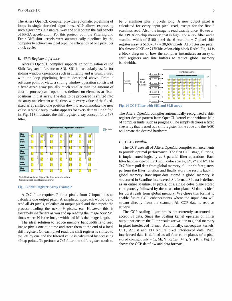
Fig. 13 Shift Register Array Example
A 7x7 filter requires 7 input pixels from 7 input lines to
calculate one output pixel. A simplistic approach would be to
read all 49 pixels, calculate an output pixel and then repeat the
process reading the next 49 pixels, etc. However this is
extremely inefficient as you end up reading the image NxM*49
times where N is the image width and M is the image length.
The ideal solution to reduce memory bandwidth is to read
image pixels one at a time and store them at the end of a local
shift register. On each pixel read, the shift register is shifted to
the left by one and the filtered value is calculated by accessing
49 tap points. To perform a 7x7 filter, the shift register needs to
be 6 scanlines plus 7 pixels long. A new output pixel is
calculated for every input pixel read, except for the first 6
scanlines read. Also, the image is read exactly once. However,
the FPGA on-chip memory cost is high. For a 7x7 filter and a
scanline width of 5100 pixel the 6 scanline + 7 pixel shift
register array is 5100x6+7 = 30,607 pixels. At 3 bytes per pixel,
it’s almost 90KB or 717Kbits of on-chip block RAM. Fig. 14 is
a block diagram of how the compiler instantiates an array of
shift registers and line buffers to reduce global memory
bandwidth.
Fig. 14 CCP Filter with SRI and SLB array
The Altera OpenCL compiler automatically recognized a shift
register design pattern from OpenCL kernel code without help
of compiler hints, such as pragmas. One simply declares a fixed
size array that is used as a shift register in the code and the AOC
will create the desired hardware.
F. CCP Dataflow
The CCP uses all of Altera OpenCL compiler enhancements
to provide optimal performance. The first CCP stage, filtering,
is implemented logically as 3 parallel filter operations. Each
filter handles one of the 3 input color spaces, L*, a* and b*. The
7x7 filters pull data from global memory, fill the shift registers,
perform the filter function and finally store the results back in
global memory. Raw input data, stored in global memory, is
structured in Scanline Interleaved, SI, format. SI data is defined
as an entire scanline, N pixels, of a single color plane stored
contiguously followed by the next color plane. SI data is ideal
for burst reads from global memory. We chose this format to
enable future CCP enhancements where the input data will
stream directly from the scanner. All CCP data is read as
uchar4.
The CCP scaling algorithm is not currently structured to
accept SI data. Since the Scaling kernel operates on Filter
output, we ensure the Filter results are written to global memory
in pixel interleaved format. Additionally, subsequent kernels,
CST, Adjust and ED require pixel interleaved data. Pixel
interleaved data is defined as all four color planes of a pixel
stored contiguously – Ci, Mi, Yi Ki Ci+1, Mi+1, Yi+1 Ki+1. Fig. 15
shows the CCP dataflow and data formats.
D Q
D Q
D Q
D Q
D Q
D Q
D Q
D Q
D Q
D Q
D Q
D Q
D Q
D Q
D Q
D Q
D Q
D Q
D Q
D Q
D Q
D Q
D Q
D Q
D Q
D Q
D Q
D Q
D Q
D Q
D Q
D Q
D Q
D Q
D Q
D Q
D Q
D Q
D Q
D Q
D Q
D Q
D Q
D Q
D Q
D Q
D Q
D Q
D Q
Multiplier/Adder Tree – Pipelined for performanceResult
D Q
Line
Buffer
Line
Buffer
Line
Buffer
Line
Buffer
Line
Buffer
Line
Buffer
Line
Buffer
Shift Register Array, D type flip flops shown in yellow
Common clock to all logic not shown
SLB/SR
SLB/SR
SLB/SR
SLB/SR
SLB/SR
7x7 Filter Matrix
DMA
Read
Channel
SLB/SR
SLB/SR
Global
Memory
D Q
D Q
D Q
D Q
D Q
D Q
D Q
D Q
D Q
D Q
D Q
D Q
D Q
D Q
D Q
D Q
D Q
D Q
D Q
D Q
D Q
D Q
D Q
D Q
D Q
D Q
D Q
D Q
D Q
D Q
D Q
D Q
D Q
D Q
D Q
D Q
D Q
D Q
D Q
D Q
D Q
D Q
D Q
D Q
D Q
D Q
D Q
D Q
D Q
Multiplier/Adder Tree – Pipelined for performanceResult
D Q

WP-01223-1.0 7
Fig. 15 CCP Kernel Dataflow
V. OPENCL SYSTEM LEVEL INTERFACES
Once the OpenCL kernel code is written and compiled it must
be packaged, loaded and executed on a reference board. Altera
provides a complete SW infrastructure to enable compilation
building, loading and utilization of the FPGA[8][9]. The Altera
OpenCL compiler takes OpenCL kernels and creates an
optimized Verilog RTL mapping. The Verilog code is then
processed using Altera’s AOC design flow resulting in an
FPGA binary programming file, called .sof. In parallel with
creating the FPGA .sof file, a standard C compiler (such as gcc)
is used to compile the C Host code that communicates with the
OpenCL kernels. The communications mechanism is through a
set of Altera OpenCL runtime libraries that are linked to the
host executable. Fig 16 shows the Altera OpenCL tool flow to
create the .sof and .exe files [9][10] .
Fig. 16 Altera OpenCL Tool Flow
A. Altera Reference Board
Altera offers multiple solutions that are compatible with
OpenCL: FPGA boards available as PCIe daughter cards and
standalone SOC/FPGA boards. We chose the Altera Cyclone V
SOC FPGA as the development platform [11]. The OpenCL
Cyclone V SOC reference platform contains the following:
Dual core ARM Cortex A9 – 800MHz
1GB of DDR3 HPS, Hard Processor System,
memory is used by Linux and is also directly
accessible to FPGA. It’s the preferred location for
OpenCL global memory.
1GB of DDR3 that is only accessible to FPGA. This
may be used as ‘scratch pad’ global memory by
OpenCL kernels.
Gigabit Ethernet to communicate with external PC
Cyclone V 5CSXFC6D6F31C8N FPGA
Fig. 17 is a block diagram of the Altera reference board used
in our design and test [12].
Fig. 17 Cyclone V SoC Reference Board Block Diagram
Scaling
R & E CST
(Lab to
CMYK)
Error Diffusion
LAB input image
(Scanline interleaved)
CMYK halftoned image stored in memory
(Pixel interleaved)
uchar4 (L1,L2,L3,L4)
uchar4 (A1,A2,A3,A4)
uchar4 (B1,B2,B3,B4)
LAB filtered image
(Pixel interleaved)
Filter
Scaling
R & EScaling
R & E
HPS DDR
Memory
Adjust
Error Diffusion
Error Diffusion
Error Diffusion
Channels datapath
Global memory datapath
uchar4 (L1,A1,B1,X1)
To maintain memory BW pixel interleaved data is written
as uchar4 where the 4th pixel is unused. While this
increases the memory buffer by 33% it greatly improves
memory BW
uchar4 (Ci,Mi,Yi,Ki)
To facilitate viewing of results
on PC, error diffused bits are NOT packed
into binary 8-bit quantities but left as bytes,
either 0x00 or 0xFF (uchar4). In a real MFP
application the binary output would be
packed into bytes and then stored
Adjust
Adjust
Adjust
Optional
FPGA DDR
Memory
CCP_kernel.clCCP.c
CLANG
front end
System
DescriptionC
compiler
ACL
runtime
Library
ccp.exe
Optimizer
Unoptimized
LLVM IR
Optimized
LLVM IR
RTL
generatorVerilog
PCIe
DDR*ACL
iFace
LLVM
front end
Unoptimized
LLVM IR
WP-01223-1.0 8
B. Altera OpenCL Interfaces
OpenCL defines a set of 4 models: Platform; Execution;
Memory; and Programming [13]. At the Platform model level
the Host is the Cyclone V SoC ARM cores and the Device is
the FPGA fabric. Within the Device we have multiple Compute
Units or CU.
Altera OpenCL models the kernel as a deeply pipelined
hardware architecture through which work-items flow. It
defines one instance of the kernel pipeline as 1 compute unit.
Programmers have the option of specifying the number of
compute units a kernel instantiates to allow for a space vs.
throughput tradeoff. Specifying a larger number of compute
units consumes more of the FPGA fabric and creates global
memory contention and constant cache contention while
increasing the effective throughput. In the CCP example, we
have 5 OpenCL kernels, namely 7x7 Filter, Scaling, CST,
Adjust and Error Diffusion, each running as 1 compute unit
concurrently.
The Execution model utilizes Altera’s OpenCL context,
Command Queue and memory objects. The CCP pipeline is a
C-based program running on one of the ARM cores. It manages
all handoffs between the Host program and the CUs in the
FPGA accelerator fabric. Fig. 18 is a simplified system software
interfaces diagram showing what elements are provided by the
user and what are provided by Altera.
Fig. 18 OpenCL System SW Interfaces
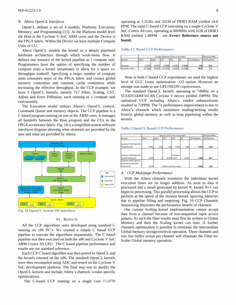
VI. RESULTS
All the CCP algorithms were developed using standard C
running on x86 PC’s. We created a simple C based CCP
pipeline to execute the algorithms sequentially. The C based
pipeline was then executed on both the x86 and Cyclone V SoC
ARM Cortex A9 CPU. The C based pipeline performance and
results are our standard reference.
Each CCP C based algorithm was then ported to OpenCL and
the kernels retested on the x86. The standard OpenCL kernels
were then recompiled using AOC and tested on the Cyclone V
SoC development platform. The final step was to modify the
OpenCL kernels and include Altera’s channels vendor specific
optimizations.
The C-based CCP running on a single core i7-3770
operating at 3.1GHz and 32GB of DDR3 RAM yielded 16.6
PPM. The same C-based CCP executing on a single Cyclone V
SoC Cortex A9 core, operating at 800MHz with 1GB of DDR3
RAM yielded 1.4PPM – see Error! Reference source not
found..
Table 1 C Based CCP Performance
Note in both C-based CCP experiments we used the highest
level of GCC Linux optimization –O3 option. However no
attempt was made to use GPU/NEON coprocessors.
The standard OpenCL kernels operating at 74MHz on a
5CSXFC6D6F31C8N Cyclone V device yielded 10PPM. The
optimized CCP including Altera’s vendor enhancements
resulted in 72PPM. The 7x performance improvement is due to
Altera’s channels which minimizes reading/writing results
from/to global memory as well as loop pipelining within the
kernels.
Table 2 OpenCL Based CCP Performance
A. CCP Multipage Performance
With the Altera channels extension the individual kernel
execution times are no longer additive. As soon as data is
processed and a result generated by kernel N, kernel N+1 can
begin its processing. This parallel processing allows the CCP to
perform at the speed of the slowest kernel, ignoring latencies
due to pipeline filling and emptying. Fig. 19 CCP Channels
Sequencing illustrates the performance benefit of channels.
Our current Scaling kernel implementation cannot accept
data from a channel because of non-sequential input access
pattern. As such the filter results must first be written to Global
Memory and then the Scaling kernel can start. A further
channels optimization is possible to eliminate the intermediate
Global memory storage/retrieval operation. Three channels and
two line buffer arrays per channel will eliminate the Filter-to-
Scaler Global memory operation.
OpenCL
Command
Queue
Memory Objects
OpenCL
HAL
OpenCL
User Space Driver
OpenCL
Linux Kernel Space
Driver
System Linux Kernel Space
Driver(s) for non-OpenCL
portions of FPGA
Device - FPGA
Application SW
MFP Copy Pipeline
OpenCL
Context
Program
KernelKernelKernel
KernelKernelKernel
Kernel Local
MemoryKernel Local
Memory
Kernel Local
Memory
User defined
Altera SDK
Altera FPGA
Key
Effective PPM
System Filter Scale CST TRC ED Full Pipeline Full Pipeline
Desktop 1.2579 0.6653 0.9238 0.0702 0.6988 3.6 16.6
Cyclone V SoC 12.1168 9.8472 10.5765 1.4193 10.1396 44.1 1.4
C Copy Pipeline (Time in seconds)
Effective PPM
System Filter Scale CST TRC ED Full Pipeline Full Pipeline
Cyclone 5 SOC OpenCL -
unoptimized 0.413 2.59 0.8 0.351 1.86 6.014 10.0
Cyclone 5 SOC OpenCL -
w/shift inference 0.474 1 0.537
included
in CST 0.475 2.486 24.1
Cyclone 5 SOC OpenCL
w/channels+SI+task
extensions 0.474 0.833 72.0
OpenCL CCP (Time in seconds)
0.359 for all four nodes
WP-01223-1.0 9
Fig. 19 CCP Channels Sequencing
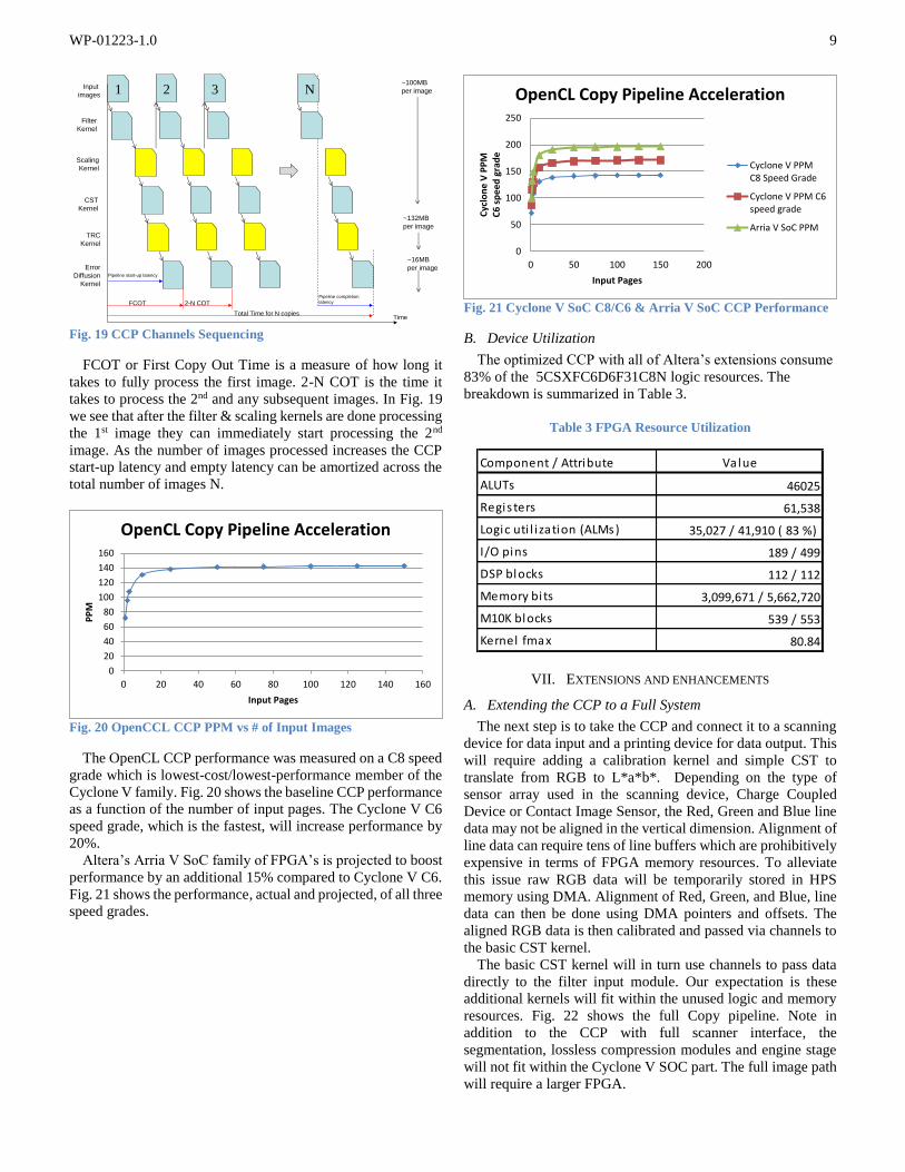
FCOT or First Copy Out Time is a measure of how long it
takes to fully process the first image. 2-N COT is the time it
takes to process the 2nd and any subsequent images. In Fig. 19
we see that after the filter & scaling kernels are done processing
the 1st image they can immediately start processing the 2nd
image. As the number of images processed increases the CCP
start-up latency and empty latency can be amortized across the
total number of images N.
Fig. 20 OpenCCL CCP PPM vs # of Input Images
The OpenCL CCP performance was measured on a C8 speed
grade which is lowest-cost/lowest-performance member of the
Cyclone V family. Fig. 20 shows the baseline CCP performance
as a function of the number of input pages. The Cyclone V C6
speed grade, which is the fastest, will increase performance by
20%.
Altera’s Arria V SoC family of FPGA’s is projected to boost
performance by an additional 15% compared to Cyclone V C6.
Fig. 21 shows the performance, actual and projected, of all three
speed grades.
Fig. 21 Cyclone V SoC C8/C6 & Arria V SoC CCP Performance
B. Device Utilization
The optimized CCP with all of Altera’s extensions consume
83% of the 5CSXFC6D6F31C8N logic resources. The
breakdown is summarized in Table 3.
Table 3 FPGA Resource Utilization
VII. EXTENSIONS AND ENHANCEMENTS
A. Extending the CCP to a Full System
The next step is to take the CCP and connect it to a scanning
device for data input and a printing device for data output. This
will require adding a calibration kernel and simple CST to
translate from RGB to L*a*b*. Depending on the type of
sensor array used in the scanning device, Charge Coupled
Device or Contact Image Sensor, the Red, Green and Blue line
data may not be aligned in the vertical dimension. Alignment of
line data can require tens of line buffers which are prohibitively
expensive in terms of FPGA memory resources. To alleviate
this issue raw RGB data will be temporarily stored in HPS
memory using DMA. Alignment of Red, Green, and Blue, line
data can then be done using DMA pointers and offsets. The
aligned RGB data is then calibrated and passed via channels to
the basic CST kernel.
The basic CST kernel will in turn use channels to pass data
directly to the filter input module. Our expectation is these
additional kernels will fit within the unused logic and memory
resources. Fig. 22 shows the full Copy pipeline. Note in
addition to the CCP with full scanner interface, the
segmentation, lossless compression modules and engine stage
will not fit within the Cyclone V SOC part. The full image path
will require a larger FPGA.
Input
images
FCOT
Filter
Kernel
Scaling
Kernel
CST
Kernel
TRC
Kernel
Error
Diffusion
Kernel
~100MB
per image
~132MB
per image
~16MB
per image
1 2 3 N
2-N COT
Pipeline start-up latency
Pipeline completion
latency
Total Time for N copiesTime
0
20
40
60
80
100
120
140
160
0 20 40 60 80 100 120 140 160
PP
M
Input Pages
OpenCL Copy Pipeline Acceleration
0
50
100
150
200
250
0 50 100 150 200
Cyc
lon
e V
PP
MC
6 s
pe
ed
gra
de
Input Pages
OpenCL Copy Pipeline Acceleration
Cyclone V PPMC8 Speed Grade
Cyclone V PPM C6speed grade
Arria V SoC PPM
Component / Attribute Value
ALUTs 46025
Regis ters 61,538
Logic uti l i zation (ALMs) 35,027 / 41,910 ( 83 %)
I/O pins 189 / 499
DSP blocks 112 / 112
Memory bits 3,099,671 / 5,662,720
M10K blocks 539 / 553
Kernel fmax 80.84

WP-01223-1.0 10
B. ARM Core(s) & NEON Coprocessing
In addition to the FPGA fabric and OpenCL the Altera SoC
family of devices have dual core ARM Cortex A9 cores with
NEON coprocessors. Certain modules of the image processing
pipeline can be offloaded to CPU(s). In particular portions of
the segmentation operation and the complete
compression/decompression function could be done using the
CPU with SIMD acceleration provided by NEON.
C. Dynamic FPGA Reprogrammability
Altera SOC FPGA’s provide dynamic reconfiguration
allowing a user to reprogram the FPGA fabric while CPU
operations continue to operate. This feature is particularly
useful in MFPs where some operations can never occur
simultaneously. For example Scan and Copy operations share 6
common input functions as shown in Fig. 22. The remaining
Copy operations, CST to Compression, and the remaining Scan
input function, JPEG compression, will never be running
simultaneously. As such we can create two sets of kernels that
include the common scanner functions and multiple backend
functions. These pipelines can be dynamically loaded based on
the MFP operations required at a given time. In a traditional
ASIC both of these modules and datapaths would have to be
included. Dynamic image path reconfiguration enables a
smaller FPGA and hence a lower cost image path.
D. Arria V and Arria 10 SOC’s
Altera’s Arria V and recently announced Arria 10 SoCs
provide a scalable platform to full featured MFP image path
solutions. Larger FPGA fabrics, increased memory, faster
clock speeds together with higher performance ARM Cores
provide a complete solution for both image processing and
general compute requirements.
Fig. 22 Full Copy and Scan Pipelines
VIII. SUMMARY AND CONCLUSIONS
OpenCL and Altera’s tool chain enabled a small team of 2
fulltime OpenCL software engineers, one fulltime hardware
engineer and other part time contributors to implement the CCP
in approximately 4.5 months. The team started with C
algorithms, created a high level C based CCP image pipeline,
ported the algorithms to OpenCL, tested the OpenCL on x86
platforms to verify basic functionality, added vendor specific
extensions, learned the Altera OpenCL tool flow and finally
tested the results on the Altera reference platform. The team
further developed a test environment to validate the correctness
of the OpenCL results at the bit level. Additionally the team
created a web based application that allows a user to select a
source image, run the image through both a C based CCP and
OpenCL accelerated CCP, display the halftoned image and
provide timing results. The software engineers had no previous
experience with FPGAs and the hardware engineer had no
previous experience with OpenCL.
This new paradigm demonstrates how quickly a small team
can go from a set of algorithms to a fully functional and
optimized pipeline implemented in hardware. Approximately
50% of the development time was devoted to optimizations
including maximizing the performance and minimizing FPGA
resource utilization. The team expects subsequent project
development times to be 50% less.
MFP vendors no longer need to invest millions of dollars and
multiple years developing ASICs or SOCs. OpenCL and Altera
SoC devices provide a new model to deliver high performance,
low cost MFP controllers in the shortest time.
IX. REFERENCES
[1] Worldwide Quarterly Hardcopy Peripherals Tracker, August 2013, International Data Corporation, Framingham, MA
[2] Rafael C. Gonzalez, Digital Image Processing (3rd Edition), Prentice
Hall, 2007
Lossless
DecompressLossless
Decompress
Engine
Interface
Calibration
& alignment
CST
(RGB to
Lab)
Filter Scaling
R & EAdjust
CST
(Lab to
CMYK)
Lossless
Compress
Error
Diffusion
RGB from
CCD or CIS
Based Scanner
Segment Image
Memory
To EngineScanner
Interface
Image
Adjust
Calibration
& alignment
CST
(RGB to
Lab)
Filter Scaling
R & E
JPEG
Compress
Segment
Export
Processing
To Network
Lossless
Compress
Image
Memory
JPEG
Decompress
JPEG
Compress
Lossless
Compress
Copy Pipeline
Scan Export Pipeline
Common kernels/modules Pipeline Specific kernels/modules
RGB from
CCD or CIS
Based Scanner
Scanner
Interface

WP-01223-1.0 11
[3] Ted Dillard, Color Pipeline: Revolutionary Paths to Controlling Digital
Color (A Lark Photography Book) Paperback, Sterling, 2009 [4] Cost effective image path for multiple office applications, by Xing Li,
Ramesh Nagarajan, Clara Cuciurean-Zapan, Francis Tse. (2012, March 6)
US Patent 8,130,389 [5] R. L. Queiroz, “Pre-Processing for MRC layers of Scanned Images,”
IEEE ICIP 2006,pp. 3093-3096, Oct. 2006
[6] Compression of mixed raster content (MRC) image data by Xing Li, Ramesh Nagarajan, Ammal Z. Malik.. (2007, March 13) US Patent
7,190,837
[7] R.W. Floyd, L. Steinberg, “An adaptive algorithm for spatial grey scale,” Proceedings of the Society of Information Display, vol. 17, pp. 75–77,
1976.
[8] Altera, Altera SoC Embedded Design Suite, 2013. [Online]. Available: http://www.altera.com/literature/ug/ug_soc_eds.pdf
[9] Altera, Altera SDK for OpenCL Programming Guide, 2013. [Online].
Available: http://www.altera.com/literature/hb/opencl-sdk/aocl_ programming_ guide.pdf
[10] Altera, Altera SDK for OpenCL Optimization Guide, 2013. [Online].
Available: http://www.altera.com/literature/hb/openclsdk/aocl_ optimization_guide.pdf
[11] Altera, Cyclone V SoC Development Board Reference Manual, 2013.
[Online]. Available: http://www.altera.com/literature/manual/ rm_cv_soc_dev_board.pdf
[12] Altera, Altera User Customizable ARM-Based SOC, 2013. [Online].
Available:http://www.altera.com/literature/br/br-soc-fpga.pdf [13] Khronos OpenCL Working Group, The OpenCL Specification, version
1.0.29, 8 December 2008. [Online]. Available: http://khronos.org/registry/cl/specs/opencl-1.0.29.pdf