Foundation Series 3.1i Quick Start Guide - uniroma2.it · Foundation Series 3.1i Quick Start Guide...
116
Foundation Series 3.1i Quick Start Guide — 0401895 Printed in U.S.A. Foundation Series 3.1i Quick Start Guide Setting Up the Foundation Tools Foundation Overview Basic Tutorial Glossary
Transcript of Foundation Series 3.1i Quick Start Guide - uniroma2.it · Foundation Series 3.1i Quick Start Guide...

Foundation Series 3.1i Quick Start Guide — 0401895 Printed in U.S.A.
Foundation Series 3.1i Quick Start Guide
Setting Up the Foundation Tools
Foundation Overview
Basic Tutorial
Glossary

Foundation Series 3.1i Quick Start Guide
Foundation Series 3.1i Quick Start Guide
Xilinx Development System
R
The Xilinx logo shown above is a registered trademark of Xilinx, Inc.
FPGA Architect, FPGA Foundry, NeoCAD, NeoCAD EPIC, NeoCAD PRISM, NeoROUTE, Timing Wizard,TRACE, XACT, XILINX, XC2064, XC3090, XC4005, XC5210, and XC-DS501 are registered trademarks of Xilinx,Inc.
The shadow X shown above is a trademark of Xilinx, Inc.
All XC-prefix product designations, Alliance Series, AllianceCORE, BITA, CLC, Configurable Logic Cell, DualBlock, EZTag, FastCLK, FastCONNECT, FastFLASH, FastMap, Foundation, HardWire, LCA, LogiBLOX, LogicCell, LogiCORE, LogicProfessor, MicroVia, Plus Logic, PLUSASM, Plustran, P+, PowerGuide, PowerMaze,SelectI/O, Select-RAM, Select-RAM+, Smartguide, SmartSearch, Smartspec, Spartan, TrueMap, UIM,VectorMaze, VersaBlock, VersaRing, Virtex, WebLINX, XABEL, XACTstep, XACTstep Advanced, XACTstepFoundry, XACT-Floorplanner, XACT-Performance, XAM, XAPP, X-BLOX, X-BLOX plus, XChecker, XDM, XDS,XEPLD, Xilinx Foundation Series, XPP, XSI, and ZERO+ are trademarks of Xilinx, Inc. The Programmable LogicCompany and The Programmable Gate Array Company are service marks of Xilinx, Inc.
All other trademarks are the property of their respective owners.
Xilinx, Inc. does not assume any liability arising out of the application or use of any product described or shownherein; nor does it convey any license under its patents, copyrights, or maskwork rights or any rights of others.Xilinx, Inc. reserves the right to make changes, at any time, in order to improve reliability, function or design andto supply the best product possible. Xilinx, Inc. will not assume responsibility for the use of any circuitry describedherein other than circuitry entirely embodied in its products. Xilinx, Inc. devices and products are protected underone or more of the following U.S. Patents: 4,642,487; 4,695,740; 4,706,216; 4,713,557; 4,746,822; 4,750,155;4,758,985; 4,820,937; 4,821,233; 4,835,418; 4,855,619; 4,855,669; 4,902,910; 4,940,909; 4,967,107; 5,012,135;5,023,606; 5,028,821; 5,047,710; 5,068,603; 5,140,193; 5,148,390; 5,155,432; 5,166,858; 5,224,056; 5,243,238;5,245,277; 5,267,187; 5,291,079; 5,295,090; 5,302,866; 5,319,252; 5,319,254; 5,321,704; 5,329,174; 5,329,181;5,331,220; 5,331,226; 5,332,929; 5,337,255; 5,343,406; 5,349,248; 5,349,249; 5,349,250; 5,349,691; 5,357,153;5,360,747; 5,361,229; 5,362,999; 5,365,125; 5,367,207; 5,386,154; 5,394,104; 5,399,924; 5,399,925; 5,410,189;5,410,194; 5,414,377; 5,422,833; 5,426,378; 5,426,379; 5,430,687; 5,432,719; 5,448,181; 5,448,493; 5,450,021;5,450,022; 5,453,706; 5,455,525; 5,466,117; 5,469,003; 5,475,253; 5,477,414; 5,481,206; 5,483,478; 5,486,707;5,486,776; 5,488,316; 5,489,858; 5,489,866; 5,491,353; 5,495,196; 5,498,979; 5,498,989; 5,499,192; 5,500,608;5,500,609; 5,502,000; 5,502,440; 5,504,439; 5,506,518; 5,506,523; 5,506,878; 5,513,124; 5,517,135; 5,521,835;5,521,837; 5,523,963; 5,523,971; 5,524,097; 5,526,322; 5,528,169; 5,528,176; 5,530,378; 5,530,384; 5,546,018;5,550,839; 5,550,843; 5,552,722; 5,553,001; 5,559,751; 5,561,367; 5,561,629; 5,561,631; 5,563,527; 5,563,528;5,563,529; 5,563,827; 5,565,792; 5,566,123; 5,570,051; 5,574,634; 5,574,655; 5,578,946; 5,581,198; 5,581,199;5,581,738; 5,583,450; 5,583,452; 5,592,105; 5,594,367; 5,598,424; 5,600,263; 5,600,264; 5,600,271; 5,600,597;5,608,342; 5,610,536; 5,610,790; 5,610,829; 5,612,633; 5,617,021; 5,617,041; 5,617,327; 5,617,573; 5,623,387;5,627,480; 5,629,637; 5,629,886; 5,631,577; 5,631,583; 5,635,851; 5,636,368; 5,640,106; 5,642,058; 5,646,545;5,646,547; 5,646,564; 5,646,903; 5,648,732; 5,648,913; 5,650,672; 5,650,946; 5,652,904; 5,654,631; 5,656,950;5,657,290; 5,659,484; 5,661,660; 5,661,685; 5,670,896; 5,670,897; 5,672,966; 5,673,198; 5,675,262; 5,675,270;5,675,589; 5,677,638; 5,682,107; 5,689,133; 5,689,516; 5,691,907; 5,691,912; 5,694,047; 5,694,056; 5,724,276;5,694,399; 5,696,454; 5,701,091; 5,701,441; 5,703,759; 5,705,932; 5,705,938; 5,708,597; 5,712,579; 5,715,197;5,717,340; 5,719,506; 5,719,507; 5,724,276; 5,726,484; 5,726,584; 5,734,866; 5,734,868; 5,737,234; 5,737,235;5,737,631; 5,742,178; 5,742,531; 5,744,974; 5,744,979; 5,744,995; 5,748,942; 5,748,979; 5,752,006; 5,752,035;5,754,459; 5,758,192; 5,760,603; 5,760,604; 5,760,607; 5,761,483; 5,764,076; 5,764,534; 5,764,564; 5,768,179;

Foundation Series 3.1i Quick Start Guide
5,770,951; 5,773,993; 5,778,439; 5,781,756; 5,784,313; 5,784,577; 5,786,240; 5,787,007; 5,789,938; 5,790,479;5,790,882; 5,795,068; 5,796,269; 5,798,656; 5,801,546; 5,801,547; 5,801,548; 5,811,985; 5,815,004; 5,815,016;5,815,404; 5,815,405; 5,818,255; 5,818,730; 5,821,772; 5,821,774; 5,825,202; 5,825,662; 5,825,787; 5,828,230;5,828,231; 5,828,236; 5,828,608; 5,831,448; 5,831,460; 5,831,845; 5,831,907; 5,835,402; 5,838,167; 5,838,901;5,838,954; 5,841,296; 5,841,867; 5,844,422; 5,844,424; 5,844,829; 5,844,844; 5,847,577; 5,847,579; 5,847,580;5,847,993; 5,852,323; 5,861,761; 5,862,082; 5,867,396; 5,870,309; 5,870,327; 5,870,586; 5,874,834; 5,875,111;5,877,632; 5,877,979; 5,880,492; 5,880,598; 5,880,620; 5,883,525; 5,886,538; 5,889,411; 5,889,413; 5,889,701;5,892,681; 5,892,961; 5,894,420; 5,896,047; 5,896,329; 5,898,319; 5,898,320; 5,898,602; 5,898,618; 5,898,893;5,907,245; 5,907,248; 5,909,125; 5,909,453; 5,910,732; 5,912,937; 5,914,514; 5,914,616; 5,920,201; 5,920,202;5,920,223; 5,923,185; 5,923,602; 5,923,614; 5,928,338; 5,931,962; 5,933,023; 5,933,025; 5,933,369; 5,936,415;5,936,424; 5,939,930; Re. 34,363, Re. 34,444, and Re. 34,808. Other U.S. and foreign patents pending. Xilinx,Inc. does not represent that devices shown or products described herein are free from patent infringement or fromany other third party right. Xilinx, Inc. assumes no obligation to correct any errors contained herein or to adviseany user of this text of any correction if such be made. Xilinx, Inc. will not assume any liability for the accuracy orcorrectness of any engineering or software support or assistance provided to a user.
Xilinx products are not intended for use in life support appliances, devices, or systems. Use of a Xilinx product insuch applications without the written consent of the appropriate Xilinx officer is prohibited.
Copyright 1991-2000 Xilinx, Inc. All Rights Reserved.

Foundation Series 3.1i Quick Start Guide — 0401895 i
About This Manual
This guide should be used as the initial learning tool for designers who are unfamiliar with the features of the Foundation series software.
Note This Xilinx software release is certified as Year 2000 compliant.
Manual ContentsThis guide covers the following topics.
• Chapter 1, “Setting Up the Foundation Tools,” gives instructions for installing Foundation 3.1i and provides you with information about the type of computer you need to successfully implement your designs.
• Chapter 2, “Foundation Overview,” looks in-depth at the capability and flexibility of the Foundation software.
• Chapter 3, “Basic Tutorial” provides a step-by-step example explaining how to use the basic Foundation tools.
• “Glossary,” defines some of the commonly used terms in this Guide.
Foundation Series 3.1i Quick Start Guide
ii Xilinx Development System
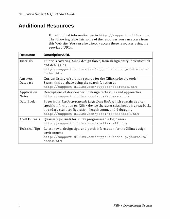
Additional Resources
For additional information, go to http://support.xilinx.com. The following table lists some of the resources you can access from this Web site. You can also directly access these resources using the provided URLs.
Resource Description/URL
Tutorials Tutorials covering Xilinx design flows, from design entry to verification and debugginghttp://support.xilinx.com/support/techsup/tutorials/index.htm
Answers Database
Current listing of solution records for the Xilinx software toolsSearch this database using the search function athttp://support.xilinx.com/support/searchtd.htm
Application Notes
Descriptions of device-specific design techniques and approacheshttp://support.xilinx.com/apps/appsweb.htm
Data Book Pages from The Programmable Logic Data Book, which contain device-specific information on Xilinx device characteristics, including readback, boundary scan, configuration, length count, and debugginghttp://support.xilinx.com/partinfo/databook.htm
Xcell Journals Quarterly journals for Xilinx programmable logic usershttp://support.xilinx.com/xcell/xcell.htm
Technical Tips Latest news, design tips, and patch information for the Xilinx design environmenthttp://support.xilinx.com/support/techsup/journals/index.htm

Foundation Series 3.1i Quick Start Guide — 0401895 iii
Conventions
This manual uses the following conventions. An example illustrates each convention.
TypographicalThe following conventions are used for all documents.
• Courier font indicates messages, prompts, and program files that the system displays.
speed grade: - 100
• Courier bold indicates literal commands that you enter in a syntactical statement. However, braces “{ }” in Courier bold are not literal and square brackets “[ ]” in Courier bold are literal only in the case of bus specifications, such as bus [7:0].
rpt_del_net=
Courier bold also indicates commands that you select from a menu.
File → Open
• Italic font denotes the following items.
♦ Variables in a syntax statement for which you must supply values
edif2ngd design_name
♦ References to other manuals

Foundation Series 3.1i Quick Start Guide
iv Xilinx Development System
See the Development System Reference Guide for more informa-tion.
♦ Emphasis in text
If a wire is drawn so that it overlaps the pin of a symbol, the two nets are not connected.
• Square brackets “[ ]” indicate an optional entry or parameter. However, in bus specifications, such as bus [7:0], they are required.
edif2ngd [option_name] design_name
• Braces “{ }” enclose a list of items from which you must choose one or more.
lowpwr ={on|off}
• A vertical bar “|” separates items in a list of choices.
lowpwr ={on|off}
• A vertical ellipsis indicates repetitive material that has been omitted.
IOB #1: Name = QOUT’
IOB #2: Name = CLKIN’
.
.
.
• A horizontal ellipsis “….” indicates that an item can be repeated one or more times.
allow block block_name loc1 loc2locn;
Online DocumentThe following conventions are used for online documents.
• Red-underlined text indicates an interbook link, which is a cross-reference to another book. Click the red-underlined text to open the specified cross-reference.

Foundation Series 3.1i Quick Start Guide v
• Blue-underlined text indicates an intrabook link, which is a cross-reference within a book. Click the blue-underlined text to open the specified cross-reference.

Foundation Series 3.1i Quick Start Guide
vi Xilinx Development System

Foundation Series 3.1i Quick Start Guide — 0401895 vii
Contents
About This ManualManual Contents ............................................................................ iAdditional Resources ..................................................................... ii
ConventionsTypographical................................................................................. iiiOnline Document ........................................................................... iv
Chapter 1 Setting Up the Foundation Tools
Installation Notes............................................................................ 1-1Supported Platforms and System Requirements...................... 1-2Memory Requirements for Xilinx Architectures......................... 1-3Installing Software..................................................................... 1-3
Installing Xilinx Software...................................................... 1-3Installing Documentation ..................................................... 1-4Installing MXE Software....................................................... 1-5
Network Compatibility ............................................................... 1-5Customer Service........................................................................... 1-6Technical Support .......................................................................... 1-6
Chapter 2 Foundation Overview
New Features................................................................................. 2-2Design Flows.................................................................................. 2-2
HDL Flow .................................................................................. 2-2Schematic Flow......................................................................... 2-3
Using the Foundation Design Entry Tools...................................... 2-6Starting the Foundation Project Manager ................................. 2-6Creating a New Project ............................................................. 2-7Creating Top-level VHDL/Verilog Designs................................ 2-8Creating Top-Level Schematic Designs.................................... 2-9

Foundation Series 3.1i Quick Start Guide
viii Xilinx Development System
Creating State Machine Designs .............................................. 2-10Instantiating LogiBLOX and CORE Generator Modules ........... 2-11Accessing the Design Entry Tools ............................................ 2-12
Using the Design Implementation Tools ........................................ 2-12Translate ................................................................................... 2-13MAP (FPGAs) ........................................................................... 2-13Place and Route (FPGAs) ........................................................ 2-14CPLD Fitter (CPLDs) ................................................................ 2-14Configure (FPGAs) ................................................................... 2-14Bitstream (CPLDs) .................................................................... 2-15Interpreting the Reports ............................................................ 2-15
Translation Report ............................................................... 2-16Map Report (FPGAs) ........................................................... 2-17Place and Route Report (FPGAs) ....................................... 2-17Pad Report (FPGAs)............................................................ 2-18Fitting Report (CPLDs) ........................................................ 2-18Post Layout Timing Report .................................................. 2-18Asynchronous Delay Report ................................................ 2-18
Selecting Options...................................................................... 2-18Using Constraint Files .................................................................... 2-20
Design, Netlist, and User Constraints ....................................... 2-20Using the Xilinx Constraints Editor............................................ 2-21Creating a User Constraints File............................................... 2-21
Static Timing Analysis .................................................................... 2-22Static Timing Analysis after Synthesis (HDL Only) ................... 2-22Static Timing Analysis after Map (FPGAs Only) ....................... 2-23Static Timing Analysis after Place and Route (FPGAs Only).... 2-23Summary Timing Reports ......................................................... 2-24Detailed Timing Analysis........................................................... 2-24
Creating Simulation Files ............................................................... 2-25When Can Simulation Data be Created?.................................. 2-25Creating Functional Simulation Data ........................................ 2-26Creating Timing Simulation Data .............................................. 2-27HDL Simulation ......................................................................... 2-28
Downloading a Design ................................................................... 2-28Creating a PROM...................................................................... 2-29In-Circuit Debugging ................................................................. 2-29
Re-Entrant Routing (FPGAs) ......................................................... 2-30
Contents
Foundation Series 3.1i Quick Start Guide ix
Chapter 3 Basic Tutorial
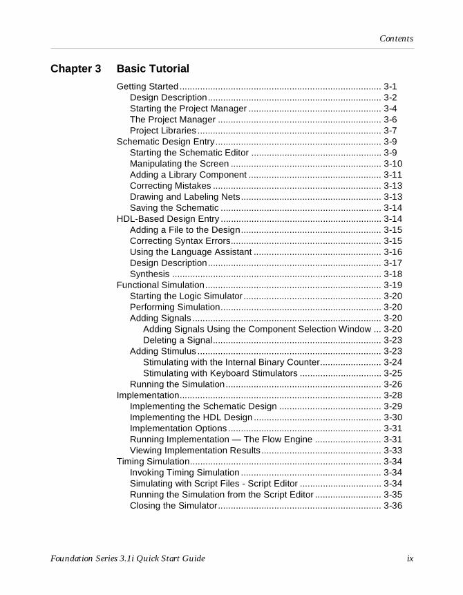
Getting Started ............................................................................... 3-1Design Description.................................................................... 3-2Starting the Project Manager .................................................... 3-4The Project Manager ................................................................ 3-6Project Libraries ........................................................................ 3-7
Schematic Design Entry................................................................. 3-9Starting the Schematic Editor ................................................... 3-9Manipulating the Screen ........................................................... 3-10Adding a Library Component .................................................... 3-11Correcting Mistakes .................................................................. 3-13Drawing and Labeling Nets....................................................... 3-13Saving the Schematic ............................................................... 3-14
HDL-Based Design Entry ............................................................... 3-14Adding a File to the Design....................................................... 3-15Correcting Syntax Errors........................................................... 3-15Using the Language Assistant .................................................. 3-16Design Description.................................................................... 3-17Synthesis .................................................................................. 3-18
Functional Simulation..................................................................... 3-19Starting the Logic Simulator ...................................................... 3-20Performing Simulation............................................................... 3-20Adding Signals .......................................................................... 3-20
Adding Signals Using the Component Selection Window ... 3-20Deleting a Signal.................................................................. 3-23
Adding Stimulus ........................................................................ 3-23Stimulating with the Internal Binary Counter........................ 3-24Stimulating with Keyboard Stimulators ................................ 3-25
Running the Simulation............................................................. 3-26Implementation............................................................................... 3-28
Implementing the Schematic Design ........................................ 3-29Implementing the HDL Design .................................................. 3-30Implementation Options ............................................................ 3-31Running Implementation — The Flow Engine .......................... 3-31Viewing Implementation Results ............................................... 3-33
Timing Simulation........................................................................... 3-34Invoking Timing Simulation ....................................................... 3-34Simulating with Script Files - Script Editor ................................ 3-34Running the Simulation from the Script Editor .......................... 3-35Closing the Simulator................................................................ 3-36

Foundation Series 3.1i Quick Start Guide
x Xilinx Development System
Glossary

Foundation Series 3.1i Quick Start Guide — 0401895 1-1
Chapter 1
Setting Up the Foundation Tools
This chapter lists the system requirements for the Foundation Series 3.1i Xilinx design tools software and discusses the recommended system types and memory requirements to comfortably run the software. Also included are general instructions for installing the software, contacting customer support, and obtaining and installing the necessary authorization codes and licenses.
For a detailed discussion, refer to the Foundation Series 3.1i Installation Guide and Release Notes.
This chapter contains the following sections:
• “Installation Notes”
• “Customer Service”
• “Technical Support”
Installation NotesEnsure the optimum use and operation of your new design tools by installing Foundation Series 3.1i on the recommended hardware with sufficient memory (RAM and hard disk “swap” space). If you experience problems with either the installation, operation, or verification of your installation, contact the Xilinx Technical Support hotline. Refer to the “Technical Support” section of this chapter for specifics.

Foundation Series 3.1i Quick Start Guide
1-2 Xilinx Development System
Supported Platforms and System RequirementsThe Foundation Series 3.1i software is a PC-only release. Foundation runs on either Windows 98/2000 or Windows NT. (Service Pack 5 or 6 is required with NT.) The following list shows the minimum recommended type of PC you should have to create designs for Xilinx FPGAs or CPLDs.
• Pentium Pro Processor®
• Windows 98®, Windows 2000®, Windows NT 4.0® (with Service Pack 5 or 6 installed)
• 120 MHz clock speed
• System Memory—32 MB to 256 MB (dependent on device)
• Swap Space—48 MB to128 MB (dependent on device)
• Required disk space, 2 GB recommended
• SVGA 17” monitor
• 4x CD-ROM drive
• Ports—Two ports (one for a pointing device and one parallel port for the parallel download cable, if needed). You can share the parallel port used for the parallel download cable.
• Keyboard
• Mouse—2-button or 3-button (Microsoft Windows compatible). On a 3-button mouse, the middle button is not used.
Note Due to the size and complexity of the XC4000 and Virtex devices, Xilinx recommends that these designs be compiled using a high-performance computer. 64 MB of RAM as well as 64 MB of swap space is required to compile XC4000EX designs, but Xilinx recommends that at least 128MB of both RAM and swap space be used. For Virtex designs, Xilinx recommends 256 MB of RAM.
Swap file size requirements also vary with the design and constraint set size. By default, Windows 98/2000 manages its swap file size automatically, but for Windows NT, you may need to increase it. Typically, your Windows NT swap file size should be twice as large as your system RAM amount.

Setting Up the Foundation Tools
Foundation Series 3.1i Quick Start Guide 1-3
It is important to note that slower systems or systems with less than the recommended RAM and swap space may exhibit longer runtimes.
Memory Requirements for Xilinx ArchitecturesThe various steps of designing Xilinx FPGAs or CPLDs require a substantial amount of memory, as shown in the following table.
Note The values given in the above table are for typical designs and include the normal load created by the operating system. Additional memory may be required for certain “boundary-case” or “extremely large” designs, as well as for concurrent operation of other non-Xilinx applications.
Installing SoftwareEnsure the optimum use and operation of your new design tools by installing the software on the recommended hardware with sufficient memory (RAM and hard disk “swap” space). If you experience problems with either the installation, operation, or verification of your installation, contact the Xilinx Technical Support hotline. Refer to the “Technical Support” section of this chapter for specifics.
Please refer to the Foundation 3.1i Installation Guide and Release Notes for complete details on installation and prerequisites for installation.
Installing Xilinx Software
This subsection explains how to install the Xilinx software tools from the Design Environment CD. Note that this CD also contains the FPGA Express software.
1. Select Start → Run. Type d:setup.exe in the Open field of the Run window and click OK. (If your CD-ROM drive is not the “d” drive, substitute the appropriate drive designation.)
Table 1-1 Minimum Memory Requirements
Xilinx Packages RAMVirtual Memory(Swap Space)
Base or Base Express 48 MB 64 MB
Foundation Express or Foundation Elite
64 MB 256 MB
Foundation Series 3.1i Quick Start Guide
1-4 Xilinx Development System
2. Follow the instructions on the screen to install the software. You will be asked to register the product from the Welcome screen during install. You can register via the web, email, or fax.
In order to register the product, you need to provide the following information:
♦ Product ID
Your product ID number is located on the back of your software CD pack.
♦ Your name
♦ Company
♦ Mailing address
♦ Phone number
♦ email address
When you register, Xilinx gives you a Registration ID. You must have the registration ID in order to complete the installation.
The installer first installs all of the Xilinx software and then invokes the installer for FPGA Express. Make sure that you install FPGA Express in the default directory indicated. Your FPGA Express synthesis FlexLM license file will be emailed to you. When install is complete, remove the CD.
You may need to reboot your PC to allow the environment variables and path statement to take effect before you can run the design implementation tools. The Install program will inform you if you need to reboot.
Installing Documentation
The documentation CD contains all of the online software manuals that can be viewed in an HTML browser. This CD also contains PDF versions of manuals that can be viewed with the Adobe Acrobat reader.
Installing the documentation is optional, that is, it is not required to run the software.
To install the Xilinx documentation CD, insert the CD and follow the instructions.

Setting Up the Foundation Tools
Foundation Series 3.1i Quick Start Guide 1-5
Installing MXE Software
This CD contains the ModelSim Xilinx Edition simulator from MTI. Installing MXE is optional; it is not required to run the software. To install the CD, perform the following steps:
1. Insert the ModelSim Xilinx Edition CD.
2. Select Start → Programs → Foundation Series 3.1i → Partner Products →Install Modelsim Xilinx Edition.
When you install this software, you are prompted for licensing. Follow the instructions on the screen to license and install the product.
3. Remove the CD when installation is complete.
Network CompatibilityThe Xilinx installation program supports only TCP-IP style networks. Novell is not a TCP-IP style network. You can run the Xilinx implementation tools from a network. However, the Aldec design entry tools, FPGA Express, and ABEL cannot be run from the network.

Foundation Series 3.1i Quick Start Guide
1-6 Xilinx Development System
Customer ServiceFor software licensing information, warranty status, shipping, and order management issues, contact Xilinx Customer Service using the information in the following table.
1 Mon-Fri, 8:00 am - 5:00 pm Pacific time2 Monday-Friday, 9:00 a.m. to 5:30 p.m. United Kingdom time—English speaking only.
If you are an international customer, contact your local sales representative for customer service issues. Refer to the Xilinx web site at http://support.xilinx.com/company/sales/int_reps.htm for contact information.
A complete list of Xilinx worldwide sales offices is at http://support.xilinx.com/company/sales/offices.htm.
Technical SupportThe following section details how to reach the Xilinx Application Service centers for your area. If you experience problems with the installation or operation of your software, Xilinx suggests that you first go to our http://support.xilinx.com website.
You can also contact the Xilinx Technical Support hotline by phone, email, or fax. When e-mailing or faxing inquiries, provide your complete name, company name, and phone number.
Country Telephone Facsimile
United States and Canada1 1-800-624-4782 408-559-0115
United Kingdom2 01932-333550 01932-828521
Belgium2 0800 73738
France2 0800 918333
Germany2 0130 816027
Italy2 1677 90403
Netherlands2 0800 0221079
Other European Locations2 (44) 1932-333550 (44) 1932-828521
Japan 81 3 3297 9153 81 3 3297 9189

Setting Up the Foundation Tools
Foundation Series 3.1i Quick Start Guide 1-7
The following table gives Worldwide contact information for Xilinx Application Service centers
Location Telephone Electronic Mail Facsimile (Fax)
North America 1-408-879-51991-800-255-7778
[email protected] 1-408-879-4442
United Kingdom 44-1932-820821 [email protected] 44-1932-828522
France 33-1-3463-0100 [email protected] 33-1-3463-0959
Germany 49-89-93088-130 [email protected] 49-89-93088-188
Japan local distributor [email protected] local distributor
Korea local distributor [email protected] local distributor
Hong Kong local distributor [email protected] local distributor
Taiwan local distributor [email protected] local distributor
Corporate Switchboard 1-408-559-7778

Foundation Series 3.1i Quick Start Guide
1-8 Xilinx Development System

Foundation Series 3.1i Quick Start Guide — 0401895 2-1
Chapter 2
Foundation Overview
This overview explains the basic concepts and design flow of the Foundation Series 3.1i release as it spans the flow from netlist to final PROM file. The chapter describes the basic tools; for details on using the tools, refer to the “Basic Tutorial” chapter.
The Foundation Overview chapter contains the following sections:
• “New Features”
• “Design Flows”
• “Using the Foundation Design Entry Tools”
• “Using the Design Implementation Tools”
• “Using Constraint Files”
• “Static Timing Analysis”
• “Creating Simulation Files”
• “Downloading a Design”
• “Re-Entrant Routing (FPGAs)”
The flow described in this chapter is generally applicable to all Xilinx families. However, many of the details apply only to the FPGA device families. For complete information on CPLD design flows, refer to the Foundation online help.

Foundation Series 3.1i Quick Start Guide
2-2 Xilinx Development System
New FeaturesThe major new features for the Foundation 3.1i release include the following:
• New Libraries for Virtex™-E, Virtex™-II and Spartan™-II
• New 3.4 version of Foundation Express
For a detailed description of these new features, refer to the What’s New file by selecting Start → Programs → Foundation Series 3.1i → What’s New.
For detailed information about Xilinx documentation, refer to the “Introduction” chapter of the Foundation Series 2.1i User Guide.
Design FlowsThe Foundation Series design tools interface supports two basic flows within the Project Manager: HDL and Schematic.
HDL FlowAn HDL Flow project can contain VHDL, Verilog, or schematic top-level designs with underlying VHDL, Verilog, or schematic modules.
HDL files can be created using the HDL Editor, Finite State Machine Editor, or other text editors. Design sources are analyzed and optimized by the Express Synthesis Engine.
LogiBLOX, CORE Generator, and ABEL modules as well as XNF files can be instantiated in the design source files using the “black box instantiation method”. Black box modules are not elaborated and optimized during synthesis. State machine modules are synthesized as VHDL or Verilog.
For a detailed description of the design methodologies, refer to the “Design Methodologies - HDL Flow” chapter in the Foundation Series 2.1i User Guide.

Foundation Overview
Foundation Series 3.1i Quick Start Guide 2-3
Schematic FlowThe Schematic Flow supports the following design strategies.
• Top-level schematic design with the Xilinx Unified Libraries components, LogiBLOX symbols, CORE generated modules, and ABEL, HDL and/or state machine macros
• Top-level ABEL-based designs (not recommended for FPGA designs)
• Top-level State Machine designs—only as ABEL designs
For a detailed description of the design methodologies, refer to the “Design Methodologies - Schematic Flow” chapter in the Foundation Series 2.1i User Guide.
Also refer to the “HDL Design Entry and Synthesis” chapter in the Foundation Series 2.1i User Guide.
The following two figures illustrate the basic design flow for FPGAs and CPLDs. For detailed design flow illustrations, refer to the “File Processing Overview” appendix in the Foundation Series 2.1i User Guide.

Foundation Series 3.1i Quick Start Guide
2-4 Xilinx Development System
Figure 2-1 Foundation Overall Design Flow for FPGAs
X8088
CHECKPOINTVERIFICATION
IMPLEMENTATION
Creation of DeviceProgramming
Data
InteractiveHardware
Debugging (Optional)
PROM FileFormatting
JTAGProgrammer
(Optional)
Multi-PassPAR
Post-Place and RouteStatic Timing Analysis
Post-MapStatic Timing
Analysis
User-Created Stimulus
User-Created Stimulus
Logic Block Delays Only
Gate-LevelFunctionalSimulation
BehavioralHDL Simulation
*
Purchased Separately
Post-Place and Route
Gate-LevelTiming Simulation
Netlist MergingMapping to Target
Architecture
Knowledge-DrivenPlace and Route
BehavioralHDL Simulation
DESIGN ENTRY
Schematic
LogiBLOXCOREGenerator
Finite StateMachine Diagram
HDL(XABEL/Verilog/
VHDL)
*
*
Foundation Overview
Foundation Series 3.1i Quick Start Guide 2-5
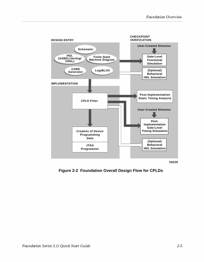
Figure 2-2 Foundation Overall Design Flow for CPLDs
CHECKPOINTVERIFICATION
IMPLEMENTATION
Creation of DeviceProgramming
Data
JTAGProgrammer
Post-ImplementationStatic Timing Analysis
User-Created Stimulus
User-Created Stimulus
Gate-LevelFunctionalSimulation
(Optional)Behavioral
HDL Simulation
(Optional)Behavioral
HDL Simulation
Post-Implementation
Gate-LevelTiming Simulation
X8228
CPLD Fitter
DESIGN ENTRY
Schematic
HDL(XABEL/Verilog/
VHDL)
Finite StateMachine Diagram
LogiBLOXCOREGenerator

Foundation Series 3.1i Quick Start Guide
2-6 Xilinx Development System
Using the Foundation Design Entry ToolsThis section describes the basic procedure for using the design entry tools.
Starting the Foundation Project ManagerTo start the Project Manager, double click the Project Manager icon in the Foundation Series program group. The icon to click is shown in the following figure.
A Getting Started dialog box displays, allowing you to select a project to open or create a new project.

Foundation Overview
Foundation Series 3.1i Quick Start Guide 2-7
Creating a New ProjectTo create a new project, follow these steps:
1. Select Create a New Project and click OK.
Figure 2-3 New Project Dialog Box
2. After the New Project dialog box displays, enter a name for the project. Change the directory for the project, if desired, by using the Browse button.
3. Choose the appropriate family, part, and speed grade and flow type. (schematic flow only)
4. Click OK. The new project displays in the Project Manager.
Foundation Series 3.1i Quick Start Guide
2-8 Xilinx Development System
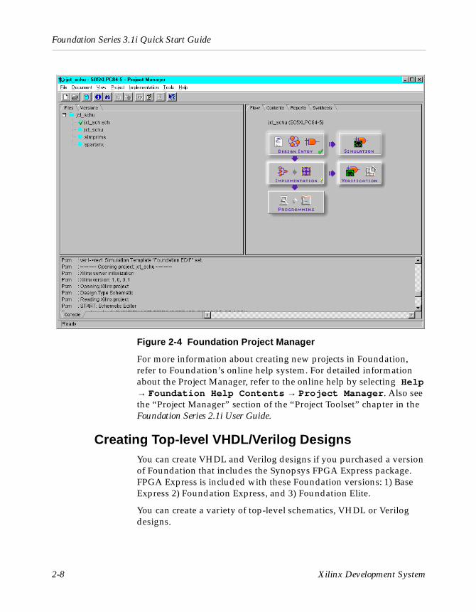
Figure 2-4 Foundation Project Manager
For more information about creating new projects in Foundation, refer to Foundation’s online help system. For detailed information about the Project Manager, refer to the online help by selecting Help → Foundation Help Contents → Project Manager. Also see the “Project Manager” section of the “Project Toolset” chapter in the Foundation Series 2.1i User Guide.
Creating Top-level VHDL/Verilog DesignsYou can create VHDL and Verilog designs if you purchased a version of Foundation that includes the Synopsys FPGA Express package. FPGA Express is included with these Foundation versions: 1) Base Express 2) Foundation Express, and 3) Foundation Elite.
You can create a variety of top-level schematics, VHDL or Verilog designs.

Foundation Overview
Foundation Series 3.1i Quick Start Guide 2-9
• All-HDL designs
• HDL designs with State Machine macros
• HDL designs with black box instantiations
• Schematic designs
Black boxes are not synthesized by Express; they are passed to the implementation tools for translation by the Flow Engine.
For a detailed description of the procedures for creating these types of designs, refer to the “Design Methodologies - HDL Flow” chapter in the Foundation Series 2.1i User Guide.
Also refer to the Foundation 3.1i Watch Tutorial located at http://support.xilinx.com/support/techsup/tutorials/index.htm.
For a discussion of HDL design issues, refer to the “HDL Design Entry and Synthesis” chapter in the Foundation Series 2.1i User Guide.
For information on how to use the VHDL and Verilog languages, refer to the online PDF documents, VHDL Reference Guide and Verilog Reference Guide.
Foundation 3.1i also includes utilities that convert ABEL and AHDL to HDL (ABEL2HDL and AHDL2HDL). To access these utilities from the Project Manager, select Tools → Utilities. In order to use ABEL or AHDL designs as top-level HDL designs, you must convert the designs.
Creating Top-Level Schematic DesignsYou can create a variety of top-level designs.
• All schematic designs
• Schematic designs with instantiated HDL macros, LogiBLOX and CORE Generator modules, and state machine macros
• Top-level ABEL-based designs
• State Machine designs—only as ABEL designs

Foundation Series 3.1i Quick Start Guide
2-10 Xilinx Development System
For a detailed description of the procedures for creating these types of designs, refer to the “In-Depth Tutorial—Schematic-Based Designs” in the Foundation 3.1i Watch Tutorial located at http://support.xilinx.com/support/techsup/tutorials/index.htm.
Also refer to the “Design Methodologies - Schematic Flow” chapter in the Foundation Series 2.1i User Guide.
For a discussion of schematic design issues, refer to the “Schematic Design Entry” chapter in the Foundation Series 2.1i User Guide.
Creating State Machine DesignsState machine designs typically start with the translation of a concept into a “paper design,” usually in the form of a state diagram or a bubble diagram. The paper design is converted to a state table and then, into the source code itself.
A State Machine design can be used in the following ways.
• Top-level design in a Schematic Flow—as an ABEL design only
• A module in a schematic
• A module in a VHDL or Verilog design (not ABEL)
For a detailed discussion of the design steps, refer to the “Design Methodologies - Schematic Flow” chapter and the “Design Method-ologies - HDL Flow” chapter in the Foundation Series 2.1i User Guide.
For a description of a sample state machine, refer to the “State Machine Designs” chapter in the Foundation Series 2.1i User Guide.

Foundation Overview
Foundation Series 3.1i Quick Start Guide 2-11
Instantiating LogiBLOX and CORE Generator Modules
LogiBLOX is a design tool for creating high-level modules such as counters, shift registers, and multiplexers for FPGA and CPLD designs. LogiBLOX includes both a library of generic modules and a set of tools for customizing these modules. LogiBLOX modules are pre-optimized to take advantage of Xilinx architectural features such as Fast Carry Logic for arithmetic functions and on-chip RAM for dual-port and synchronous RAM. With LogiBLOX, you can create high-level LogiBLOX modules that will fit into your schematic-based design or HDL-based design.
For information about instantiating LogiBLOX into designs, refer to the following sections in the Foundation Series 2.1i User Guide:
• “Schematic Designs With Instantiated LogiBLOX Modules” section of the “Design Methodologies - Schematic Flow” chapter
• “HDL Designs with Black Box Instantiation” section of the “Design Methodologies - HDL Flow” chapter of the Foundation Series 2.1i User Guide
The Xilinx CORE Generator tool is a design tool that delivers parame-terizable cores, optimized for Xilinx FPGAs. The CORE Generator library includes cores as complex as DSP filters and multipliers and as simple as delay elements. You can use these cores as building blocks in order to complete your design more quickly. In Foundation 3.1i, the CORE Generator tools are integrated into the Project Manager, Schematic Editor, and HDL Editor. For details on how to instantiate cores in schematics, refer to the “Schematic Designs With Instantiated CORE Generator Cores” section of the “Design Method-ologies - Schematic Flow” chapter. For details on how to instantiate cores in HDL designs, refer to the “CORE Generator COREs in a VHDL or Verilog Design” section of the “Design Methodologies - HDL Flow” chapter of the Foundation Series 2.1i User Guide.
For complete information about the CORE Generator tool, refer to the online manual, CORE Generator User Guide.
Foundation Series 3.1i Quick Start Guide
2-12 Xilinx Development System
Accessing the Design Entry ToolsYou can access all of the Design Entry tools from the Project Manager ’s Tools menu (Tools → Design Entry). The tools include the following:
• Schematic Editor
• State Editor
• HDL Editor
• Symbol Editor
• LogiBLOX module generator
• CORE Generator
You can also directly access the Schematic Editor, State Editor, and HDL Editor from the Design Entry phase button.
For a complete description on how to use these design entry tools, see the Foundation Series 2.1i User Guide.
After completing a design with design entry, the design is next implemented to a target Xilinx hardware part.
Using the Design Implementation ToolsThe implementation tools perform the translate map, place, route, (fit for CPLDs), and bitstream generation phases of the design flow
The Xilinx Flow Engine is the graphical interface that displays each of of these design phases. Results of these implementations are made available in reports and may be accessed through the Reports tab in the Project Manager.
The Foundation Project Manager provides menu and push button access to other Xilinx tools such as the Timing Analyzer, PROM File Formatter, Floorplanner, FPGA Editor, Constraints Editor, and CPLD ChipViewer. You can access these tools through either the Tools menu or Implementation menu in the Project Manager or directly from the Project Flowchart push buttons.

Foundation Overview
Foundation Series 3.1i Quick Start Guide 2-13
During design implementation, the Flow Engine prominently displays the status of each phase of the design, as shown in the following figures.
Figure 2-5 Flow Engine Shows All Design Segments Completed (FPGAs)
Figure 2-6 Flow Engine Shows All Design Segments Completed (CPLDs)
TranslateThe Flow Engine’s first step, Translate, merges all of the input netlists. This is accomplished by running NGDBuild. For a complete description of NGDBuild, refer to the “NGDBuild” chapter of the Development System Reference Guide.
MAP (FPGAs)The next step is the technology mapper. Map optimizes the gates and trims unused logic in the merged NGD netlist. This step also maps the design’s logic resources; logic in the design is mapped to resources on the silicon, and a physical design rule check is performed. For more information about MAP, refer to the “MAP—The Technology Mapper” chapter in the online software manual, Development System Reference Guide.
Foundation Series 3.1i Quick Start Guide
2-14 Xilinx Development System
Place and Route (FPGAs)After the design is mapped, the Flow Engine places and routes the design. In the place stage, all logic blocks, including the configurable logic blocks (CLB) and input/output blocks (IOB) structures, are assigned to specific locations on the die.
If timing constraints have been placed on particular logic components, the placer tries to meet those constraints by moving the corresponding logic blocks closer together.
In the routing stage, the logic blocks are assigned specific intercon-nect elements on the die. If timing constraints have been placed on particular logic components, the router tries to meet those constraints by choosing a faster interconnect. For more information about PAR, refer to the “PAR—Place and Route” chapter in the online software document, Development System Reference Guide.
CPLD Fitter (CPLDs)The CPLD fitter implements designs for the XC9500 and XC9500XL devices. The fitter outputs several files: fitting report (design_name.rpt), static timing report (design_name.tim), guide file (design_name.gyd, programming file (design_name.jed), and timing simulation database (design_name.nga).
For detailed information about implementing CPLD designs, refer to the Foundation online help.
Configure (FPGAs)After place and route, the Flow Engine translates the physical imple-mentation into a configuration file (bit) that is used to program the FPGA. The BitGen executable creates the configuration file. For more information about the BitGen executable, refer to the “BitGen” chapter in the online software document, Development System Refer-ence Guide.
You can program an FPGA using the Hardware Debugger or JTAG Programmer to download a bitstream to configure a device. You can also use a bitstream as an input to the PROM File Formatter, which creates a specific configuration program for PROM use.

Foundation Overview
Foundation Series 3.1i Quick Start Guide 2-15
Bitstream (CPLDs)At the end of a successful CPLD implementation, a .jed programming file is created. The JTAG Programmer uses this file to configure XC9500/XL CPLD devices.
Interpreting the ReportsThe reports generated by the implementation tools provide information on logic trimming, logic optimization, timing constraint performance, and I/O pin assignment. To access the reports, select the Reports tab from Project Manager. Double click the Implementation Report Files icon to open the Report Browser. To open a particular report, double click its icon, as shown in the following two figures.
Figure 2-7 Report Browser (FPGAs)

Foundation Series 3.1i Quick Start Guide
2-16 Xilinx Development System
Figure 2-8 Report Browser (CPLDs)
Translation Report
The translation report (.bld) contains warning and error messages from the three translation processes: conversion of the EDIF or XNF style netlist to the Xilinx NGD netlist format, timing specification checks, and logical design rule checks. The report lists the following:
• Missing or untranslatable hierarchical blocks
• Invalid or incomplete timing constraints
• Output contention, loadless outputs, and sourceless inputs

Foundation Overview
Foundation Series 3.1i Quick Start Guide 2-17
Map Report (FPGAs)
The Map Report (.mrp) contains warning and error messages detailing logic optimization and problems in mapping logic to physical resources. The report lists the following information:
• Removed logic. Sourceless and loadless signals can cause a whole chain of logic to be removed. Each deleted element is listed with progressive indentation, so the origins of removed logic sections are easily identifiable; their deletion statements are not indented.
• Logic that has been added or expanded to optimize speed.
• The Design Summary section lists the number and percentage of used CLBs, IOBs, flip-flops, and latches. It also lists occurrences of architecturally-specific resources like global buffers and boundary scan logic.
Note The Map Report can be very large. To find information, use key word searches. To quickly locate major sections, search for the string ‘---‘, because each section heading is underlined with dashes.
Place and Route Report (FPGAs)
The Place and Route Report (.par) contains the following information.
• The overall placer score which measures the “goodness” of the placement. Lower is better. The score is strongly dependent on the nature of the design and the physical part that is being targeted, so meaningful score comparisons can only be made between iterations of the same design targeted for the same part.
• The Number of Signals Not Completely Routed should be zero for a completely implemented design. If non-zero, you may be able to improve results by using re-entrant routing or the multi-pass place and route flow.
• The timing summary at the end of the report details the design’s delays. For information on timing constraint performance and synchronous delays, refer to the “Static Timing Analysis” section later in this chapter

Foundation Series 3.1i Quick Start Guide
2-18 Xilinx Development System
Pad Report (FPGAs)
The Pad Report lists the design’s pinout in three ways.
• Signals are referenced according to pad numbers.
• Pad numbers are referenced according to signal names.
• PCF file constraints are listed.
Fitting Report (CPLDs)
The Fitting Report (design_name.rpt) lists summary and detailed information about the logic and I/O pin resources used by the design, including the pinout, error and warning messages, and Boolean equations representing the implemented logic.
Post Layout Timing Report
A timing summary report shows the calculated worst-case timing for the logic paths in your design.
Asynchronous Delay Report
This report shows the 20 worst net delays within the design.
Selecting OptionsOptions specify how a design is optimized, mapped, placed, routed, and configured. Options are grouped into objects called implementation, simulation, and configuration templates. Each template defines an implementation, simulation or configuration approach. For example, one implementation style could be Quick Evaluation, while another could be Timing Constraint Driven.

Foundation Overview
Foundation Series 3.1i Quick Start Guide 2-19
Figure 2-9 Flow Engine Options Dialog Box
You can have multiple templates in a project. To access the options and templates, perform the following steps.
1. Select the Options button in the Implement or Synthesis/Implementation dialog box.
2. In the Program Option portion of the Options dialog box, select the Edit Template button for Implementation, Simulation, or Configuration to access the associated template.
The default options settings provide sufficient performance for most design requirements. For information on the options, select Help → Help Topics from the Flow Engine menu.

Foundation Series 3.1i Quick Start Guide
2-20 Xilinx Development System
Using Constraint FilesWith the design implementation tools, you can control the implementation of a design by entering constraints. There are two basic types of constraints that you can apply to a design: location constraints and timing constraints.
Location constraints are used to control the mapping and positioning of the logic elements in the target device. The most common location constraints are pad constraints. They are used to lock the pins of the design to specific I/O locations so that the pin placement is consistent from revision to revision.
Timing constraints tell the software which paths are critical, and therefore, need closer placement and faster routing. Conversely, timing constraints also tell the software which paths are not critical and, therefore, do not need closer placement or faster routing. Both the placer and the router can be timing constraint driven.
Design, Netlist, and User ConstraintsConstraints can be entered throughout the design entry and implementation processes. Constraints can be entered during the design entry phase by adding them to a schematic, specifying them through the use of a constraint entry GUI, or listing them in a user constraint file (.ucf). These three approaches differ in the following ways.
• Constraints entered directly in the input design are known simply as design constraints and are ultimately placed in the design netlist.
• If you want your constraints separated from the input design files, or if you want to modify your constraints without having to completely re-synthesize your design, you can use the Xilinx Constraints Editor or create a user constraints file design_name.ucf.
Foundation Overview
Foundation Series 3.1i Quick Start Guide 2-21
Using the Xilinx Constraints EditorThe Constraints Editor is a Graphical User Interface (GUI) that you can run after the Translate program to create new constraints in a UCF file. To access the Constraints Editor, select Tools → Imple-mentation → Constraints Editor from the Project Manager.
The Constraints Editor interface consists of a main window, three tab windows, and a number of dialog boxes. For more details, refer to the online software document, Constraints Editor Guide.
You can also directly enter constraints into a UCF file without using the Xilinx Constraints Editor. See the next section for details.
Creating a User Constraints FileThe User Constraints File (.ucf) is a user-created ASCII file that holds timing and location constraints. It is read by NGDBuild during the translate process and is combined with an EDIF or XNF netlist into an NGD file. If a UCF file exists with the same name as the top-level netlist, then it will automatically be read. Otherwise, specify a file for User Constraints in the Implement Control Files Settings dialog box.
For Foundation 3.1i, if you already have an existing UCF file associated with a Revision, this UCF file is automatically copied and used as your UCF file within a new revision.
Note Xilinx recommends that you use the Xilinx Constraints Editor to edit a UCF file. If you edit an existing UCF manually, make sure that you are editing the correct file.
For an example of how to lock I/Os to pin locations and how to write Timespec and Timegroup constraints, refer to the “Foundation Constraints” appendix in the Foundation Series 2.1i User Guide.
You can also lock pin locations within the Project Manager by selecting Tools → Implementation → Lock Device Pins.

Foundation Series 3.1i Quick Start Guide
2-22 Xilinx Development System
Static Timing AnalysisYou can perform timing analysis at several stages in the implementation flow to estimate delays. You create or generate the following.
• A post-synthesis pre-implementation display for HDL designs with the Express Time Tracker (Foundation Express only—not Base Express).
• A post-map timing report to evaluate the effects of logic delays on timing constraints.
• A post-place-and-route timing report that incorporates both block and routing delays as a final analysis of the design’s timing constraints.
The Interactive Timing Analyzer tool produces detailed timing constraint, clock, and path analysis for post-map or post-place-and-route implementations.
Note Static timing analysis may make the implementation processes run slower.
Static Timing Analysis after Synthesis (HDL Only)You can examine static timing results with the Express Time Tracker after synthesis and before implementation. You must be licensed to use Foundation Express to access the Time Tracker and the Express Constraints Editor.
1. After you synthesize your design, right click the optimized structure from the Versions tab.
2. Select View Synthesis Results.
3. Select the Paths tab from the Time Tracker to view estimated delays.

Foundation Overview
Foundation Series 3.1i Quick Start Guide 2-23
Static Timing Analysis after Map (FPGAs Only)Post-map timing reports can be very useful in evaluating timing performance. Although route delays are not accounted for, the logic delays can provide valuable information about the design.
If logic delays account for a significant portion (> 50%) of the total allowable delay of a path, the path may not be able to meet your timing requirements when routing delays are added.
Routing delays typically account for 40% to 60% of the total path delays. By identifying problem paths, you can mitigate potential problems before investing time in place and route. You can redesign the logic paths to use less levels of logic, tag the paths for specialized routing resources, move to a faster device, or allocate more time for the path.
If logic-only-delays account for much less (<35%) than the total allowable delay for a path or timing constraint, then the place-and-route software can use very low placement effort levels. In these cases, reducing effort levels allow you to decrease runtimes while still meeting performance requirements.
Static Timing Analysis after Place and Route (FPGAs Only)
Post-PAR timing reports incorporate all delays to provide a comprehensive timing summary. If a placed and routed design has met all of your timing constraints, then you can proceed by creating configuration data and downloading a device. On the other hand, if you identify problems in the timing reports, you can try fixing the problems by increasing the placer effort level, using re-entrant routing, or using multi-pass place and route. You can also redesign the logic paths to use fewer levels of logic, tag the paths for specialized routing resources, move to a faster device, or allocate more time for the paths.
For information on re-entrant routing or multi-pass place and route, see the “Re-Entrant Routing (FPGAs)” section at the end of this chapter.

Foundation Series 3.1i Quick Start Guide
2-24 Xilinx Development System
Summary Timing ReportsSummary reports show timing constraint performance and clock performance. Implementing a design in the Flow Engine can automatically generate summary timing reports. To create summary timing reports, perform the following steps:
1. Open the Options dialog box (Implementation → Options) from the Project Manager and select Edit Options for the Implementation template.
2. Select the Timing Reports tab.
3. For a post-map report, select Produce Logic Level Timing Report. For a post-PAR report, select Produce Post Layout Timing Report
4. To modify the reports to highlight path delays or paths that have failed timing constraints, select a report format.
5. After MAP or PAR has completed, the respective timing reports appear in the Report Browser.
Detailed Timing AnalysisTo perform detailed timing analysis, select Tools → Simulation/Verification → Interactive Timing Analyzer from the Project Manager menu. You can specify specific paths for analysis, discover paths not affected by timing constraints, and analyze the timing performance of the implementation based on another speed grade. For path analysis, perform the following:
1. Choose sources. From the Timing Analyzer menu, select Path Filters → Custom Filters → Select Sources.
2. Choose destinations. From the Timing Analyzer menu, select Path Filters → Custom Filters → Select Destinations.
3. To create a report, select one of the options under the Analyze menu.
To switch speed grades, select Options → Speed Grade. After a new speed grade is selected, all new Timing Analyzer reports will be based on the design running with new speed grade delays. The design does not have to be re-implemented, because the new delays are read from a separate data file.

Foundation Overview
Foundation Series 3.1i Quick Start Guide 2-25
Creating Simulation FilesAfter the design is implemented, you can perform a timing simulation to ascertain if the timing requirements and functionality of your design have been met. Timing simulation can save considerable time by reducing the time spent debugging test boards in the lab. Functional simulation can also potentially save time by uncovering design bugs before running PAR.
When Can Simulation Data be Created?With the design implementation tools, you can create simulation data after each major processing step. This means that you can create functional simulation netlists after NGDBuild merges the design together in the Translate process and simulation netlists after PAR has placed and routed the design for FPGAs or the CPLD fitter has fit the design for CPLDs.
Additionally, for FPGAs, you can create simulation data after the design has been mapped. For a graphical representation of when you can conveniently simulate your design, refer to Figure 2-1 and Figure 2-2.
For FPGAs, simulation data created after the design has been mapped contains timing data based on the CLB and IOB block delays, and all net (interconnect) delays are set to zero.
With post-map simulation, you can ensure that the design’s current implementation will give the place and route software sufficient margin to route the design and still stay within your timing requirements.
Simulation data created after the design has been placed, but not routed, contains accurate block delays and estimates for the net delays.
You can use post-place simulation as an incremental simulation step between post-map simulation and a complete post-route timing simulation.
To simulate at any of these intermediate stages, select Tools → Simulation/Verification → Checkpoint Gate Simulation Control from the Foundation Project Manager and choose the appropriate netlist to simulate.

Foundation Series 3.1i Quick Start Guide
2-26 Xilinx Development System
Creating Functional Simulation DataFor schematic and HDL designs, the functional simulation netlists are created in the Foundation design entry tools environment. Click the Simulation phase button in the Project Manager Flowchart area to invoke the Simulator and load the netlist. The Simulation phase button is shown in the following figure.
For designs that include macros whose underlying files are XNF or EDIF netlists, the design must first be “translated” in the Xilinx implementation tools in order to merge in these additional netlists. Follow these steps to translate the design and then invoke the simulator and load the functional netlist.
1. Select Project → Create Version from the Project Manager.
2. Select Project → Create Revision from the Project Manager.
3. Select Tools → Implementation → Flow Engine from the Project Manager while the new revision is selected in the Versions tab.
4. From within the Flow Engine, select Setup → Stop After and then choose the Stop After Translate option.
5. Click OK, then select File → Run in the Flow Engine.
6. After Translate is complete, go back to the Foundation Project Manager and select Tools → Simulation/Verification → Checkpoint Gate Simulation Control.
7. Choose the appropriate NGD file from the Revision which was just created and click OK. This invokes the simulator and loads the netlist.
For details about functional simulation, refer to the “Functional Simulation” chapter in the Foundation Series 2.1i User Guide and the “In-Depth Tutorial—Functional Simulation” chapter in the Founda-tion 3.1i Watch Tutorial located at http://support.xilinx.com/support/techsup/tutorials/index.htm.
Foundation Overview
Foundation Series 3.1i Quick Start Guide 2-27
For additional information about functional simulation, see the “Performing Functional Simulation” section of the “Design Method-ologies - Schematic Flow” chapter in the Foundation Series 2.1i User Guide.
Creating Timing Simulation DataBefore you perform timing simulation, ensure that you have gener-ated a timing annotated simulation netlist. See the “Timing Simula-tion” section of the “Verification and Programming” chapter in the Foundation Series 2.1i User Guide for details and the “In-Depth Tuto-rial—Timing Simulation” chapter in the Foundation 3.1i Watch Tutorial located at http://support.xilinx.com/support/techsup/tutorials/index.htm.
1. To create the timing simulation netlist, open the Options dialog box by selecting Implementation → Options, and verify that Foundation EDIF displays in the Simulation list box for Program Options.
2. Click OK.
3. After the Implementation process is complete, return to the Foundation Project Manager, and click the timing simulation portion of the Verification phase button. This invokes the Simulator and loads the timing simulation netlist.
For additional information about timing simulation, refer to the “Verifying the Design” section of the “Design Methodologies - Sche-matic Flow” chapter in the Foundation Series 2.1i User Guide.
Foundation Series 3.1i Quick Start Guide
2-28 Xilinx Development System
HDL SimulationFoundation provides the option of adding HDL simulation capabilities to all Foundation design flows. Xilinx ships an evaluation version of an HDL simulator from MTI.
This product may be licensed for free evaluation for up to 30 days. Sale and support for this product is provided directly by the vendors.
All ModelSim product sales are handled directly by MTI and its authorized sales affiliates (email [email protected]).
Customer support is also provided directly by MTI (email [email protected] or call the main number at (503) 641-1340)
Adding MTI’s ModelSim product to the Foundation Series design environment enables simulation of VHDL, Verilog HDL or mixed-HDL designs (Verilog and VHDL). Source code debugging, functional simulation, and back-annotated timing simulation are all supported through this integrated solution. The availability of a mixed-language simulation environment offers maximum flexibility to HDL design methodologies which draw on design elements from both Verilog and VHDL.
Downloading a DesignYou can download an implemented FPGA design directly from your PC using the Hardware Debugger program with the XChecker cable, JTAG download cable, or MultiLINX cable. No cables are shipped with the Foundation product.
The Hardware Debugger can download a BIT file or a PROM file: MCS, EXO, or TEK file formats. A BIT file contains configuration information for an FPGA device. For more information on using the Hardware Debugger, see the Hardware Debugger Guide.
You can download an implemented CPLD design from your PC using the JTAG Programmer. The JTAG Programmer software is used to configure FPGAs and CPLDs and supports both the XChecker and the Parallel Cable III. This is a GUI based program. See the JTAG Programmer Guide for details. Also, see the Hardware User Guide for information about cable compatibility.
To download an implemented design, click the Programming icon in the Project Flow area.
Foundation Overview
Foundation Series 3.1i Quick Start Guide 2-29
Creating a PROMAn FPGA or daisy chain of FPGAs can be configured from serial or parallel PROMs. The PROM File Formatter can create MCS, EXO, or TEK style files. The files are read by a PROM programmer that turns the image into a PROM.s
A HEX file can also be used to configure an FPGA or a daisy chain of FPGAs through a microprocessor. The file is stored as a data structure in the microprocessor boot-up code.
In-Circuit DebuggingOnce a design has been downloaded to an FPGA, snapshots of internal signal states can be captured and read using the Hardware Debugger program with the XChecker cable, JTAG cable, or MultiLINX cable. You can display the signal states as waveforms in the Hardware Debugger.
This capability allows you to test and debug your design in a real-time environment as it interfaces with the other components on your board. You can also control the states of your state machines by controlling when clock edges are sent to your system clock input.
For more information on in-circuit debugging and the Hardware Debugger, see the Hardware Debugger Guide.
Foundation Series 3.1i Quick Start Guide
2-30 Xilinx Development System
Re-Entrant Routing (FPGAs)The place and route software, PAR, has features that allow it to process complex designs that have tight timing requirements and/or are difficult to route. If your design is completely placed and routed but not meeting timing specifications, PAR can start from where it left off and continue re-routing the design to produce an implementation that meets your timing specifications.
As PAR is running, it continually updates the NCD file with its current placement and routing information. As long as an NCD file exists that is at least placed, PAR can used it for re-entrant routing. To initiate re-entrant routing, follow these steps.
1. In the Project Manager, select Tools → Implementation → Flow Engine.
2. In the Flow Engine, select the Setup → FPGA Re-entrant Route menu.
3. In the Setup Re-entrant Route dialog box, select Allow Re-Entrant Route, which enables the re-entrant route options:
♦ Optional: If meeting timing specifications is a critical goal, then select Use Timespecs During Re-entrant Route. If meeting timing specifications is not critical, do not select this option, because timing-driven routing takes much longer to process than non-timing-driven routing
♦ Optional: Select the number of re-entrant routing passes to perform. If left in “Auto,” PAR will continue to perform routing iterations until either 1) it determines that it is no longer making significant progress, or 2) the design constraints have been fully met.
♦ Optional: Select the number of clean-up passes to run. Clean-up passes are run after the “main” routing passes are complete. Two types of clean-up routing passes can be invoked—cost-based and delay-based. The effectiveness of each type depends on the design, device, and constraints of the implementation.

Foundation Overview
Foundation Series 3.1i Quick Start Guide 2-31
4. Click OK (in the Setup Re-entrant Routing dialog box) to submit the options. This causes the Place and Route icon in the Flow Engine to show a loop back arrow and the Re-Entrant route label.
If you are specifying timing or location constraints, you have the option to relax them to give PAR more flexibility. If you modify the UCF file, you must step backwards with the Flow Engine and re-run Translation in order to incorporate the changes.

Foundation Series 3.1i Quick Start Guide
2-32 Xilinx Development System
Foundation Series 3.1i Quick Start Guide — 0401895 3-1
Chapter 3
Basic Tutorial
This tutorial describes the features in the Foundation Series release 3.1i. The tutorial is provided in three separate types of projects:
• schematic
• Verilog
• VHDL
The chapter contains the following sections:
• “Getting Started”
• “Schematic Design Entry”
• “HDL-Based Design Entry”
• “Functional Simulation”
• “Implementation”
• “Timing Simulation”
Getting StartedThis section guides you through a typical FPGA-based design procedure using a design called ”JCOUNT.” The JCOUNT design targets a SpartanXL device—S05XLPC84-5; however, all of the principles and flows taught are applicable to any Xilinx device family, unless otherwise noted.
In the first part of the tutorial, you will use the Foundation design entry tools to complete the design. The design is composed of flip-flops, buffers, and pads.

Foundation Series 3.1i Quick Start Guide
3-2 Xilinx Development System
Design DescriptionThroughout this tutorial, the design is referred to as JCOUNT.
The design begins as an unfinished design. After you complete the design, you will simulate it to verify the functionality.
“JCOUNT” is a simple 4-bit Johnson counter. The completed schematic is shown in the following picture.
Figure 3-1 Completed JCOUNT Schematic
Controls:
• CLK—input clock pulse
• CE—clock enable (when set to 0, the counter freezes)
• CLR—clear input (when set to 1, the counter is reset to all zeroes)
Basic Tutorial
Foundation Series 3.1i Quick Start Guide 3-3
Outputs:
Q0-Q3—counter outputs
Operation:
The counter is triggered on the rising edge of the clock (CLK) when the clock enable signal (CE) is high. Following is the sequence of states during normal operation (that is, without clearing of the counter):
0000
0001
0011
0111
1111
1110
1100
1000
0000
There are also two files external to the project that contain simulation results.
• JCT_F.TVE—prerouted design simulation results
• JCT_T.TVE—routed design timing simulation results

Foundation Series 3.1i Quick Start Guide
3-4 Xilinx Development System
Starting the Project ManagerThis tutorial assumes that the Foundation software is installed in the default location c:\fndtn. If you have installed the software in a different location, substitute your installation path for c:\fndtn.
The JCOUNT project is installed in the c:\fndtn\active\projects directory. Following is the list of JCOUNT projects supplied by Xilinx.
1. Double click the Foundation Series Project Manager icon on your desktop or select Start → Programs → Foundation Series 3.1i → Xilinx Project Manager from the Start menu icon in the lower left corner of your screen.
2. A Getting Started dialog box displays, allowing you to select a project to open. If you have not opened this tutorial project before now, click the More Projects... button.
Project Name Description
JCT_SCHF JCOUNT schematic -- finished
JCT_SCHU JCOUNT schematic -- unfinished
JCT_VHDF JCOUNT VHDL -- finished
JCT_VHDU JCOUNT VHDL -- unfinished
JCT_VERF JCOUNT Verilog -- finished
JCT_VERU JCOUNT Verilog -- unfinished
Basic Tutorial
Foundation Series 3.1i Quick Start Guide 3-5
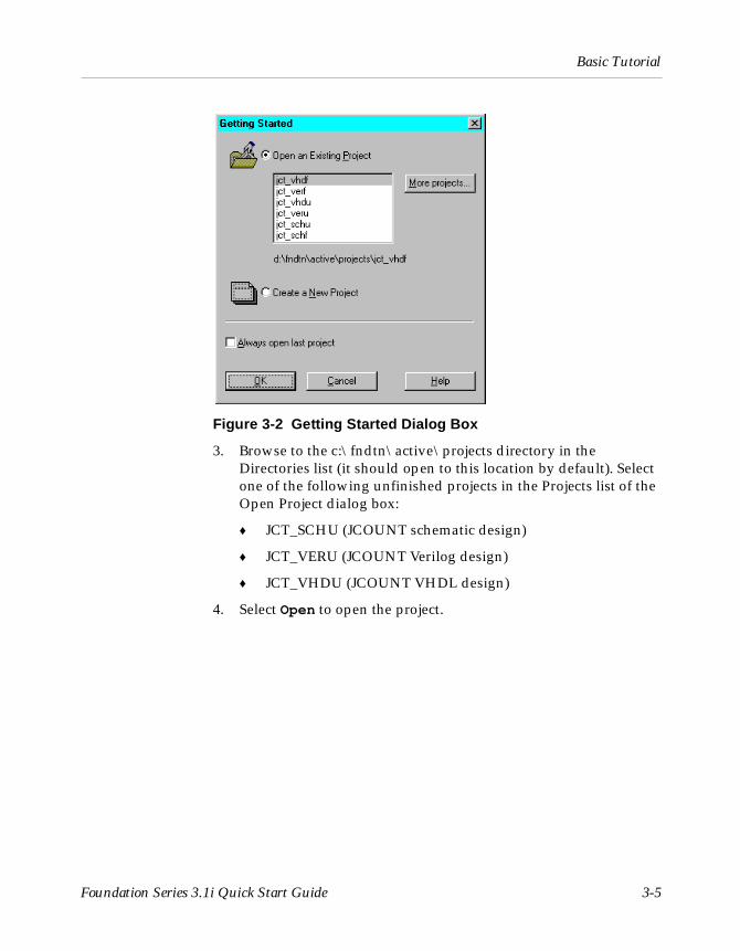
Figure 3-2 Getting Started Dialog Box
3. Browse to the c:\fndtn\active\projects directory in the Directories list (it should open to this location by default). Select one of the following unfinished projects in the Projects list of the Open Project dialog box:
♦ JCT_SCHU (JCOUNT schematic design)
♦ JCT_VERU (JCOUNT Verilog design)
♦ JCT_VHDU (JCOUNT VHDL design)
4. Select Open to open the project.

Foundation Series 3.1i Quick Start Guide
3-6 Xilinx Development System
The Project ManagerThe Project Manager controls all aspects of the design flow. You can access all of the various design entry and design implementation tools as well as the files and documents associated with your project. The Project Manager also maintains revision control over multiple design iterations.
The Project Manager is divided into three main subwindows. To the left is the Design Hierarchy Browser which displays the project elements. To the right is a set of tabs, each one opens a separate functional window. The third window at the bottom of the Project Manager is the Message Console and shows status messages, errors, and warnings and is updated during all project actions.
Figure 3-3 Project Manager (Schematic Design)

Basic Tutorial
Foundation Series 3.1i Quick Start Guide 3-7
Figure 3-4 Project Manager (HDL Design)
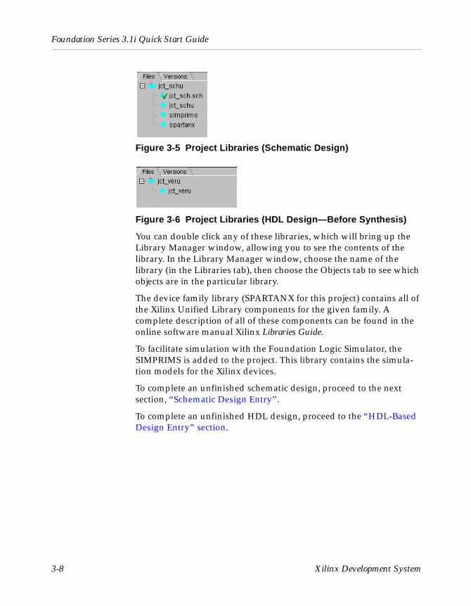
Project LibrariesFor schematic designs, when you create a new project in Foundation, three libraries are automatically added to the project: the appropriate device family library based on the target family you have chosen (for example, SPARTANX), the project library (with the same name as the project), and the SIMPRIMS library (for simulation). All libraries that are part of the project are listed in the Files tab of the Project Manager.
For HDL designs, only the project library is initially added to the project. All other libraries are added after synthesis and display in the Files tab.
Foundation Series 3.1i Quick Start Guide
3-8 Xilinx Development System
Figure 3-5 Project Libraries (Schematic Design)
Figure 3-6 Project Libraries (HDL Design—Before Synthesis)
You can double click any of these libraries, which will bring up the Library Manager window, allowing you to see the contents of the library. In the Library Manager window, choose the name of the library (in the Libraries tab), then choose the Objects tab to see which objects are in the particular library.
The device family library (SPARTANX for this project) contains all of the Xilinx Unified Library components for the given family. A complete description of all of these components can be found in the online software manual Xilinx Libraries Guide.
To facilitate simulation with the Foundation Logic Simulator, the SIMPRIMS is added to the project. This library contains the simula-tion models for the Xilinx devices.
To complete an unfinished schematic design, proceed to the next section, “Schematic Design Entry”.
To complete an unfinished HDL design, proceed to the “HDL-Based Design Entry” section.

Basic Tutorial
Foundation Series 3.1i Quick Start Guide 3-9
Schematic Design EntryThis section explains how to complete the unfinished schematic design, JCT_SCHU. If you selected an HDL design instead, proceed to the “HDL-Based Design Entry” section.
Starting the Schematic EditorYou can start the Schematic Editor in either of these ways:
• From the Flow tab, click the Schematic Editor icon in the Design Entry phase button. This instructs the Schematic Editor to open the project’s top level schematic sheet.
• Double click the file name jct_sch.sch in the Files tab.
The Schematic Editor opens with the jct_sch.sch schematic sheet loaded. The jct_sch.sch schematic is incomplete at this point. You will now complete it.
If you need to stop the tutorial at any time, save your work on the schematic by selecting File → Save from the schematic pulldown menus.

Foundation Series 3.1i Quick Start Guide
3-10 Xilinx Development System
Figure 3-7 Schematic Editor
Manipulating the ScreenUnder the Display pulldown menu is a series of commands that modify the viewing area of the Schematic Editor window. Zoom in or out of the schematic to comfortably view it.

Basic Tutorial
Foundation Series 3.1i Quick Start Guide 3-11
Adding a Library ComponentComponents from all of the libraries (except SIMPRIMS) for the given project are available from the SC (Schematic) Symbols Toolbox to place on the schematic. The available components listed in this toolbox are arranged alphabetically within each library.
1. From the pulldown menus of the schematic editor, select Mode → Symbols or click the Symbols Toolbox button in the vertical toolbar on the left side of the Schematic Editor.
This puts the schematic editor in “Symbols Mode,” opens the SC Symbols window, and displays the libraries and their corre-sponding components.
Figure 3-8 SC Symbols Toolbox

Foundation Series 3.1i Quick Start Guide
3-12 Xilinx Development System
2. The component you will place is an IPAD input pad. You can select this component by either scrolling down the list and selecting it or by typing IPAD in the bottom of the SC Symbols Window. Then, move the mouse back into the schematic window.
In the SC Symbols window, when the IPAD component is selected, a description of the component appears in the bottom of the window.
3. Move the symbol outline to the location shown at the lower left of the following picture and click the left mouse button to place the IPAD between the CE and CLR IPADs.
Remove the SC Symbols window by toggling the Symbols Toolbox icon on the vertical toolbar (“un-click” to exit the toolbox mode).
You will wire up the IPAD later in the tutorial. For now, just place it on the schematic.
Figure 3-9 Placing IPAD
Basic Tutorial
Foundation Series 3.1i Quick Start Guide 3-13
Correcting MistakesIf you make a mistake when placing the component, you can easily move or delete the component.
1. Press the Esc key on the keyboard to exit the Symbols Mode.
2. Select the component you want to move or delete. Make sure that no other components are selected (clicking a blank area of the schematic deselects everything).
3. Click and drag to correctly place the component, or press the Del key on the keyboard or the Cut icon in the toolbar to delete the component.
Drawing and Labeling NetsYou use the Draw Wires icon in the vertical toolbar to draw wires (also called nets) to connect the IPAD to other components on the schematic.
1. Click the Draw Wires icon in the vertical toolbar.
2. Click the source pin (output pin of the IPAD), then click the destination pin (the IBUF to the right of the IPAD that connects to the flip-flop clock). The net will automatically be drawn between the two pins.
Note You can specify the shape of the net by moving the mouse in the direction you want to draw the net and then single-clicking to create a 90-degree bend in the wire. If you make a mistake while drawing a net, you can quit your current drawing by pressing the “Escape” key.
3. Press the “Escape” key to return to Select-and-Drag mode.
4. Double click the net that you just drew.
5. In the Net Name field, type CLK as shown below.

Foundation Series 3.1i Quick Start Guide
3-14 Xilinx Development System
Figure 3-10 Labeling Nets
6. Click OK. Now, view your net, labeled, on the schematic sheet.
Saving the SchematicThe jct_sch.sch schematic is now complete.
Save the schematic by selecting File → Save or clicking the Save icon in the horizontal toolbar.
All errors, warnings, and informational messages are displayed in the Message Window in the Project Manager. If any errors are issued, resolve them and save the schematic again.
Proceed to the “Functional Simulation” section
HDL-Based Design EntryIn this section, you will use either one of two HDL projects: jct_veru or jct_vhdu. This is the same JCOUNT design that is used in the schematic design entry. However, rather than being comprised of modules on a schematic sheet, this JCOUNT design is written in VHDL or Verilog.
This section assumes that you have already opened one of the following HDL example designs from the Project Manager.
• c:\fndtn\active\projects\jct_veru
• c:\fndtn\active\projects\jct_vhdu

Basic Tutorial
Foundation Series 3.1i Quick Start Guide 3-15
Adding a File to the DesignFor this tutorial, you will add either the Verilog file (.v) or the VHDL file (.vhd) to the design. Each design has a syntax error. To add the file to the design and fix the errors, perform the following steps:
1. Add the Jct_ver.v or the Jct_vhd.vhd file to the project by selecting Document → Add. After the Add Document dialog box displays, enter the Jct_ver.v or Jct_vhd.vhd file name in the File name list box and click Open.
Note that the file has a red X next to it. The red X means that the file has an error.
2. Double click the Jct_ver.v or the Jct_vhd.vhd in the Files tab of the Project Manager file to open it.
Correcting Syntax ErrorsThe following steps explain how to correct syntax errors.
1. Check the syntax of the HDL file you are using by selecting Synthesis → Check Syntax from within the HDL Editor. Both the Jct_ver.v and Jct_vhd.vhd file have the same syntax error—the CLK port is not declared.
♦ If you are using the Jct_ver.v file, add the CLK definition to Line 1. Line 1 should look like the following after adding the CLK definition.
module JCT_VER (CLK, CE, CLR, Q);
♦ If you are using the Jct_vhd.vhd file, add the CLK declaration to the Port declaration. The Port declaration lines should look like the following after adding the CLK declaration.
port (CLK: in STD_LOGIC;
CE: in STD_LOGIC;
CLR: in STD_LOGIC;
Q: inout STD_LOGIC_VECTOR (3 downto 0));
2. Recheck the syntax. The designs now check successfully.

Foundation Series 3.1i Quick Start Guide
3-16 Xilinx Development System
Using the Language AssistantWhile you are in the HDL editor, view the Language Assistant. The Language Assistant provides templates (example code fragments) for commonly used HDL constructs, as well as synthesis templates for commonly used logic components such as counters, D flip-flops, multiplexers, and global buffers. You can add your own templates to the Language Assistant for components or constructs you use often.
1. To invoke the Language Assistant, select Tools → Language Assistant from the HDL Editor pulldown menu.
2. The Language Assistant is divided into three sections: Language Templates, Synthesis Templates, and User Templates. To expand the view of any of these sections, click the ‘+’ next to the topic. Click any of the listed templates to view the HDL code in the right hand pane.
3. Notice the template called D Flip Flop, located under the Flip Flops heading within the Synthesis Templates and the corresponding HDL code in the right-hand window.
Figure 3-11 HDL Language Assistant
4. Close the Language Assistant by clicking the “X” in the top right corner of its window.
5. Close the HDL editor (do not make any modifications) by selecting File → Exit.

Basic Tutorial
Foundation Series 3.1i Quick Start Guide 3-17
Design DescriptionThe HDL design used in this tutorial is either a top-level Verilog or VHDL design file. To ensure that the file has recently been analyzed by Foundation Express, choose Synthesis → Analyze all Sources.
HDL files that make up a project always have one of four status indicators associated with the file. Examples of these indicators are shown below:
A red question mark means that the file has been modified and needs to be re-analyzed. Right-click the file and select Analyze from the pulldown menu.
A red exclamation point means warnings have been issued. Select the file and examine the warnings under the HDL Warnings tab. To investigate the warning on a file, perform the following steps:
1. Click the file name.
2. Click the HDL Warnings tab in the messages window.
3. Single-click to highlight the warning message
4. Press the “F1” key on your keyboard. An extended help message screen will pop up. Many synthesis warnings may be safely ignored.
A red X means errors have been found.
A green check mark means that the file is up-to-date with no errors or warnings.

Foundation Series 3.1i Quick Start Guide
3-18 Xilinx Development System
SynthesisNow that the design has been entered and each file analyzed, you will synthesize the design in the next steps. “Logic Synthesis” is the process of compiling your HDL code into an XNF or EDIF netlist of gates. That netlist is the input to the Xilinx Implementation Tools. In this section, you will “pull” the design completely through synthesis.
1. Set the global synthesis options by selecting Synthesis → Options. Set the Default Frequency to 100 (default is 50 MHz), and check the Export Timing Constraints box. Click OK to accept these values.
2. Click the + next to jct_ver.v or jct_vhd.vhd. This shows the modules within the HDL file.
3. Select the module named “JCT_VER” or “JCT_VHD” and click the Synthesis button from the Flow tab.
This step causes the flow to proceed through Synthesis.
4. In the Synthesis/Implementation window, complete the Target Device fields with this information:
♦ Family: SPARTANXL
♦ Device: S05XLPC84
♦ Speed Grade: -5

Basic Tutorial
Foundation Series 3.1i Quick Start Guide 3-19
Figure 3-12 Synthesis/Implementation Window
Note If your design is JCT_VHD, then “JCT_VHD” displays in the Top level field instead of “JCT_VER”.
5. Click Run.
Foundation Express synthesizes and optimizes the design and also creates a design version.
6. Proceed to the next section, “Functional Simulation”.
Functional SimulationYou can perform functional simulation before design implementation to verify that the logic that you have created is correct. Foundation provides a Logic Simulator, which is a gate-level simulator. You can perform functional simulation on a schematic-based design immediately after you have finished using the Schematic editor. In a later section, you will perform timing simulation, which takes place after the design is implemented (placed and routed) with the Xilinx Implementation Tools.

Foundation Series 3.1i Quick Start Guide
3-20 Xilinx Development System
Starting the Logic SimulatorClick the Simulation phase button in the Project Flowchart.
You may be prompted to update the schematic netlist if you modified the design but did not write out a netlist. In this case, click Yes to update the netlist. (If you also get a dialog asking to update macros, select No. You will get this dialog only if you inadvertently changed something in the HDL editor.)
The Logic Simulator is invoked, and the project netlist is automatically loaded into the simulator.
Performing SimulationThere are three basic steps to simulate your design:
1. Adding signals - the inputs and outputs you want to see in the simulator
2. Adding stimulus - inputs on some of the signals
3. Running the simulation - and view output waveforms
Adding SignalsIn order to view signals during the simulation, you must first add them to the Waveform Viewer in the Simulator. The signals are then listed in the Waveform Viewer. You can view and monitor the waveforms next to the corresponding signal names.
Adding Signals Using the Component Selection Window
Follow these steps to add signals using the Component Selection window within the Simulator.
1. Click the Component Selection icon in the toolbar in the Simulator or select Signal → Add Signals.
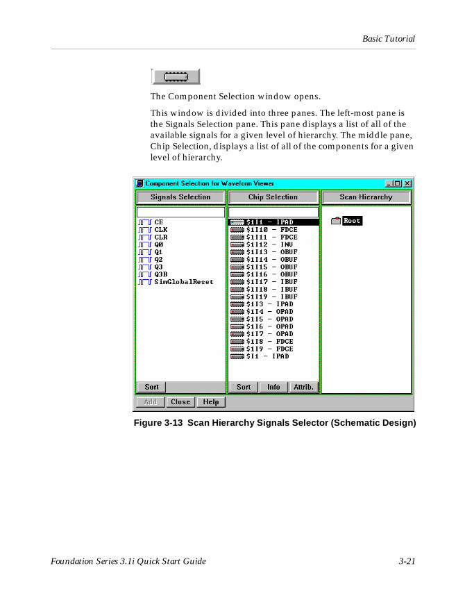
Basic Tutorial
Foundation Series 3.1i Quick Start Guide 3-21
The Component Selection window opens.
This window is divided into three panes. The left-most pane is the Signals Selection pane. This pane displays a list of all of the available signals for a given level of hierarchy. The middle pane, Chip Selection, displays a list of all of the components for a given level of hierarchy.
Figure 3-13 Scan Hierarchy Signals Selector (Schematic Design)

Foundation Series 3.1i Quick Start Guide
3-22 Xilinx Development System
Figure 3-14 Scan Hierarchy Signals Selector (HDL Design)
2. From the Signals Selection pane, you can either double click signals to add them to the Waveform Viewer, or you can single click and then press Add. Use whichever method you prefer to add the following nets and buses:
CLK
CE
CLR
<Q3, Q0> (4-bit wide Q bus)
3. (Schematic design only) Create a bus for the output signals Q3, Q2, Q1, and Q0.
a) Shift click each Q output.
b) With all four outputs selected, right-click the mouse and select Bus → Combine.
(The HDL design Q outputs are already defined as a bus).

Basic Tutorial
Foundation Series 3.1i Quick Start Guide 3-23
4. Change the radix of the Q bus to binary.
a) Select Q.
b) Right-click the mouse button and select Bus → Display Binary.
5. Close the Component Selection Window by clicking the Close button.
All of the signals you added are now in the Waveform Viewer.
Deleting a Signal
To delete any of the signals from the Waveform Viewer, first select the signal in the signal list in the Waveform Viewer, right-click, and then select Delete Signals → Selected. This operation removes the highlighted signal from the Waveform Viewer.
Adding StimulusTo define the function of the input signals, you must add stimulus to your simulation. There are many ways to define stimulus with the Foundation Simulator. In this tutorial, you will use the keyboard stimulus.
Open the Stimulator Selection Window by clicking the Stimulator icon in the toolbar or by selecting Signal → Add Stimulators...
The Stimulator Selection window appears:

Foundation Series 3.1i Quick Start Guide
3-24 Xilinx Development System
Figure 3-15 Stimulator Selector
Stimulating with the Internal Binary Counter
You need to simulate an input clock for the JCOUNT design, so you will use the Foundation Simulator ’s internal 16-bit binary counter. Use the least-significant bit (LSB) of the counter (B0). The right-most round yellow LED in the Stimulator Selection window is the B0 counter.
To simulate the system clock, you assign the B0 stimulus to the CLK signal in the simulator.
1. In the Waveform Viewer, select the CLK signal by clicking it.
2. In the Stimulator Selection Window, click the B0 stimulator (the right-most yellow round LED). You should now see a B0 next to the CLK signal in the Waveform Viewer indicating that the B0 stimulator is assigned to CLK.
3. Select Options → Preferences from the Simulator window. This opens the Preferences window. In the Simulation tab of this window, you can set the frequency of the B0 counter output. Set the B0 frequency to 10MHz.

Basic Tutorial
Foundation Series 3.1i Quick Start Guide 3-25
Figure 3-16 Simulator Preferences
4. Click OK to close the Preferences window.
Stimulating with Keyboard Stimulators
You assign keyboard keys as stimulus for signals in your design with the keyboard in the Stimulator Selection window. After you assign a key as a stimulus, the signal’s value toggles between 1 and 0 when-ever you press the corresponding key on your PC’s keyboard.
Assign the R keyboard stimulus to the CLR signal in the JCOUNT design.
1. Click and drag the R key on the keyboard in the Stimulator Selector onto the CLR signal name in the Waveform Viewer.
2. You should now see an r next to the CLR signal in the Waveform Viewer, which indicates that this is the assigned stimulus.
3. Press the R key on your PC keyboard a few times to see the state of the stimulus toggling in the Waveform Viewer.
4. In the same way, assign the E keyboard stimulus to the CE signal in the JCOUNT design.
5. Close the Stimulator Selection window by clicking its Close button.
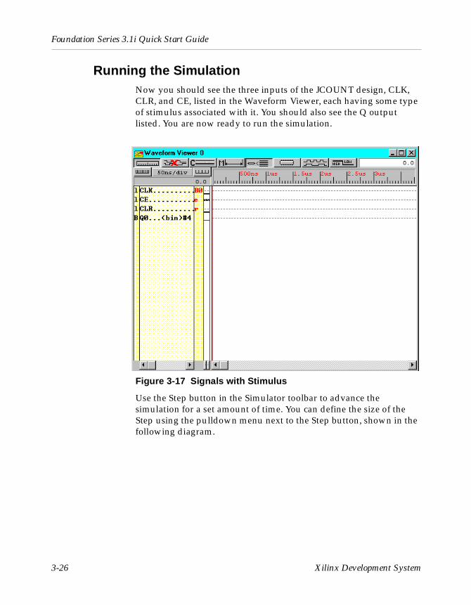
Foundation Series 3.1i Quick Start Guide
3-26 Xilinx Development System
Running the SimulationNow you should see the three inputs of the JCOUNT design, CLK, CLR, and CE, listed in the Waveform Viewer, each having some type of stimulus associated with it. You should also see the Q output listed. You are now ready to run the simulation.
Figure 3-17 Signals with Stimulus
Use the Step button in the Simulator toolbar to advance the simulation for a set amount of time. You can define the size of the Step using the pulldown menu next to the Step button, shown in the following diagram.
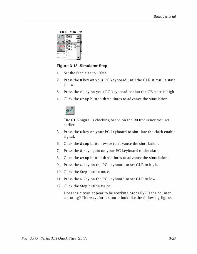
Basic Tutorial
Foundation Series 3.1i Quick Start Guide 3-27
Figure 3-18 Simulator Step
1. Set the Step size to 100ns.
2. Press the R key on your PC keyboard until the CLR stimulus state is low.
3. Press the E key on your PC keyboard so that the CE state is high.
4. Click the Step button three times to advance the simulation.
The CLK signal is clocking based on the B0 frequency you set earlier.
5. Press the E key on your PC keyboard to simulate the clock enable signal.
6. Click the Step button twice to advance the simulation.
7. Press the E key again on your PC keyboard to simulate.
8. Click the Step button three times to advance the simulation.
9. Press the R key on the PC keyboard to set CLR to high.
10. Click the Step button once.
11. Press the R key on the PC keyboard to set CLR to low.
12. Click the Step button twice.
Does the circuit appear to be working properly? Is the counter counting? The waveform should look like the following figure.

Foundation Series 3.1i Quick Start Guide
3-28 Xilinx Development System
Figure 3-19 Resulting Waveform
13. To clear your waveforms and start your simulation over, choose Waveform → Delete → All Waveforms with Power On from the Simulator pulldown menus.
14. Run several simulations, experimenting with the CLR and CE input functionality.
15. Close the Logic Simulator window by selecting File → Exit.
ImplementationThis section describes how to implement a design.
• If you created the schematic design, proceed to the “Implementing the Schematic Design” section.
• If you created the HDL design, proceed to the “Implementing the HDL Design” section.
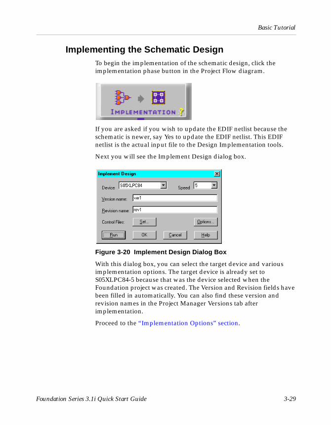
Basic Tutorial
Foundation Series 3.1i Quick Start Guide 3-29
Implementing the Schematic DesignTo begin the implementation of the schematic design, click the implementation phase button in the Project Flow diagram.
If you are asked if you wish to update the EDIF netlist because the schematic is newer, say Yes to update the EDIF netlist. This EDIF netlist is the actual input file to the Design Implementation tools.
Next you will see the Implement Design dialog box.
Figure 3-20 Implement Design Dialog Box
With this dialog box, you can select the target device and various implementation options. The target device is already set to S05XLPC84-5 because that was the device selected when the Foundation project was created. The Version and Revision fields have been filled in automatically. You can also find these version and revision names in the Project Manager Versions tab after implementation.
Proceed to the “Implementation Options” section.

Foundation Series 3.1i Quick Start Guide
3-30 Xilinx Development System
Implementing the HDL DesignIn the “Synthesis” section, you synthesized your design. To implement the design, perform the following steps.
1. Click the Implementation phase button in the Project Flow diagram.
2. The Revision Name is automatically filled in with “rev1”. If you want to use a new name, enter it in the box. Proceed to the “Implementation Options” section.
Figure 3-21 Synthesis/Implementation Dialog Box

Basic Tutorial
Foundation Series 3.1i Quick Start Guide 3-31
Implementation OptionsImplementation options specify how a design is optimized, mapped, placed, routed, and configured. Options are grouped into objects called implementation, simulation, and configuration templates. Each template defines an implementation, simulation or configuration approach.
1. Click the Options button. The Options dialog box opens.
2. Select desired options and click OK.
Figure 3-22 Options Dialog Box
3. Click OK to close the Options dialog box.
Running Implementation — The Flow EngineAfter setting the implementation options, you are ready to implement the design.
Click Run in the Implement Design dialog box or click Run in the Synthesis/Implementation dialog box.
The Flow Engine displays and processes your design through the implementation steps.

Foundation Series 3.1i Quick Start Guide
3-32 Xilinx Development System
Figure 3-23 Flow Engine
When implementation is complete, the Flow Engine closes automati-cally, and the Foundation Series Project Manager is fully visible again. Click OK in the Flow Engine Completed Successfully dialog box.
The status of the implementation is displayed in the console window at the bottom of the Project Manager. You should see (OK Implemented) and Completed Successfully for the version and revision. If you encountered any errors in the implementation, refer to the Implementation Log file for details on the error.
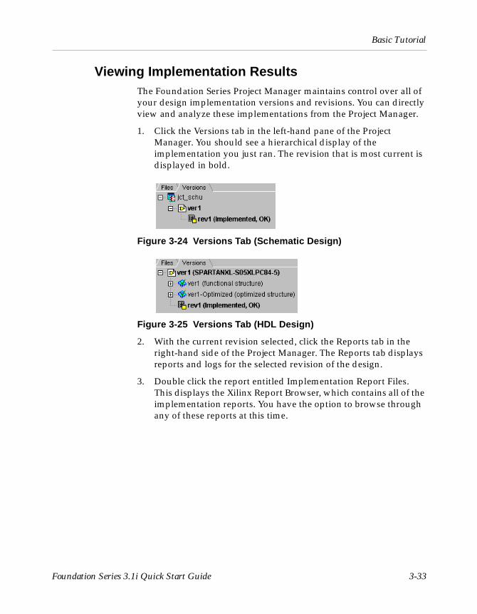
Basic Tutorial
Foundation Series 3.1i Quick Start Guide 3-33
Viewing Implementation ResultsThe Foundation Series Project Manager maintains control over all of your design implementation versions and revisions. You can directly view and analyze these implementations from the Project Manager.
1. Click the Versions tab in the left-hand pane of the Project Manager. You should see a hierarchical display of the implementation you just ran. The revision that is most current is displayed in bold.
Figure 3-24 Versions Tab (Schematic Design)
Figure 3-25 Versions Tab (HDL Design)
2. With the current revision selected, click the Reports tab in the right-hand side of the Project Manager. The Reports tab displays reports and logs for the selected revision of the design.
3. Double click the report entitled Implementation Report Files. This displays the Xilinx Report Browser, which contains all of the implementation reports. You have the option to browse through any of these reports at this time.

Foundation Series 3.1i Quick Start Guide
3-34 Xilinx Development System
Timing SimulationTiming simulation uses the block and routing delay information from the routed design to give a more accurate assessment of the behavior of the circuit under worst-case conditions. For this reason, timing simulation is performed after the design has been placed and routed.
This section of the tutorial shows how to run a script to do a simulation. Timing simulation uses the same tools as does the functional simulation that you did with the design earlier. The only difference is that the design which is loaded into the simulator for timing simulation contains worst-case routing delays based on the actual placed and routed design.
Invoking Timing SimulationTo invoke the timing simulator, click the Timing Simulation icon in the Verification phase button in the Project Manager Flow diagram.
The simulator is now loaded and ready to simulate. For this simulation, you will use an existing script file.
Simulating with Script Files - Script EditorEarlier, you used the Foundation Series functional simulator to input signals to the simulator and to provide stimulus including keyboard stimulus and the internal binary counter. In this section, you use a script file to simulate the design and will launch it from the Script Editor.
1. To invoke the Script Editor, select Tools → Script Editor from the pulldown menus within the Simulator. A dialog box prompts you to select a script file.
2. Choose Open: Existing Script File and click OK.
3. Select the file: jcount.cmd, which was written previously for you to use in this tutorial.

Basic Tutorial
Foundation Series 3.1i Quick Start Guide 3-35
Browse the script file; you will notice the same inputs and outputs that you used in the functional simulation earlier.
Running the Simulation from the Script EditorThis section explains how to run simulation from the script editor.
1. You can execute the simulation directly from the Script Editor. To do this, select Execute → Go.
A log of the executed commands appears at the bottom of the Script Editor.
2. To view the simulation results in the Waveform Viewer, move the Script Editor window and bring the Waveform Viewer window to the front of your view.
3. Click the Expand icon located above the signal names display to view the waveform in more details.
4. Inspect the simulation results to make sure they are accurate.
You should now see that this is indeed performing a timing simulation based on actual delays in the placed and routed design. If you zoom in to get a closer view of the waveforms, you will see that there is a delay from the rising edge of the clock to the transitions or the counter outputs.
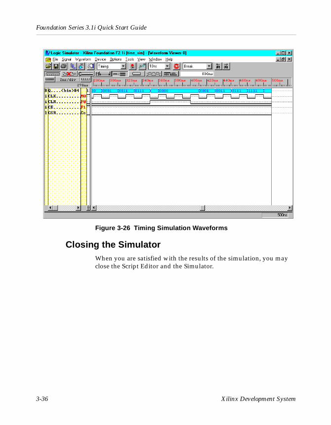
Foundation Series 3.1i Quick Start Guide
3-36 Xilinx Development System
Figure 3-26 Timing Simulation Waveforms
Closing the SimulatorWhen you are satisfied with the results of the simulation, you may close the Script Editor and the Simulator.
Foundation Series 3.1i Quick Start Guide — 0401895 Glossary-1
Glossary
ABELABEL is a high-level language (HDL) and compilation system produced by Data I/O Corporation.
actionsIn state machines, actions are HDL statements that are used to make assignments to output ports or internal signals. Actions can be executed at several points in a state diagram. The most commonly used actions are state actions and transition actions. State actions are executed when the machine is in the associated state. Transition actions are executed when the machine goes through the associated transition.
AldecAn Electronic Design Automation (EDA) vendor. Aldec provides the Foundation Project Manager, Schematic Editor, Logic Simulator, and HDL Editor, and State Editor.
aliasesAliases, or signal groups, are useful for probing specific groups of nodes.
analyzeThe Foundation Express process in which design source files are examined for correct syntax.

Foundation Series 3.1i Quick Start Guide
Glossary-2 Xilinx Development System
architectureArchitecture is the common logic structure of a family of programmable integrated circuits. The same architecture can be realized in different manufacturing processes. Examples of Xilinx architectures are the XC4000, XC5200, and XC9500 devices.
attributesAttributes are instructions placed on symbols or nets in an FPGA schematic to indicate their placement, implementation, naming, direction, or other properties.
back-annotationBack-annotation is the translation of a routed or fitted design to a timing simulation netlist.
BitGenA program that produces a bitstream for Xilinx device configuration. BitGen takes a fully routed NCD (Circuit Description) file as its input and produces a configuration bitstream, a binary file with a .bit extension.
Black Box InstantiationInstantiation where the synthesizer is not given the architecture or modules. In Foundation, black boxes are translated with the implementation tools.
blockA block is a group of one or more logic functions. A block is a schematic or symbol sheet. There are four types of blocks.
• A Composite block indicates that the design is hierarchical.
• A Module block is a symbol with no underlying schematic.
• A Pin block represents a schematic pin.
• An Annotate block is a symbol without electrical connectivity that is used only for documentation and graphics.

Foundation Series 3.1i Quick Start Guide Glossary-3
breakpointA breakpoint is a condition for which a simulator must stop to perform simulation commands.
bufferA buffer is an element used to increase the current or drive of a weak signal and, consequently, increase the fanout of the signal. A storage element.
busA bus is a group of nets carrying common information. In LogiBLOX, bus sizes are declared so that they can be expanded accordingly during design implementation.
CLBThe Configurable Logic Block (CLB). Constitutes the basic FPGA cell. It includes two 16-bit function generators (F or G), one 8-bit function generator (H), two registers (flip-flops or latches), and reprogrammable routing controls (multiplexers).
CLBs are used to implement macros and other designed functions. They provide the physical support for an implemented and downloaded design. CLBs have inputs on each side, and this versatility makes them flexible for the mapping and partitioning of logic.
componentA component is an instantiation or symbol reference from a library of logic elements that can be placed on a schematic.
conditionA condition is a Boolean expression. If there is more than one transition leaving a state in a state machine, you must associate a condition with each transition.

Foundation Series 3.1i Quick Start Guide
Glossary-4 Xilinx Development System
constraintConstraints are specifications for the implementation process. There are several categories of constraints: routing, timing, area, mapping, and placement constraints.
Using attributes, you can force the placement of logic (macros) in CLBs, the location of CLBs on the chip, and the maximum delay between flip-flops. CLBs are arranged in columns and rows on the FPGA device. The goal is to place logic in columns on the device to attain the best possible placement from the standpoint of both performance and space.
constraints editorA GUI tool that you can use to enter design constraints. In Foundation 3.1i, there are two constraint editors. The Express editor is available only in the Foundation Express product configuration. The Xilinx Constraints Editor is integrated with the Design Implementation tools and available in all product configurations.
constraint fileA constraint file specifies constraints (location and path delay) information in a textual form. An alternate method is to place constraints on a schematic.
CORE Generator toolA software tool for generating and delivering parameterizable cores optimized for FPGAs. The library includes cores as complex as DSP filters and multipliers and as simple as delay elements. You can use these cores as building blocks in order to complete your designs more quickly.

Foundation Series 3.1i Quick Start Guide Glossary-5
CPLDComplex Programmable Logic Device (CPLD) is an erasable programmable logic device that can be programmed with a schematic or a behavioral design. CPLDs constitute a type of complex PLD based on EPROM or EEPROM technology. They are characterized by an architecture offering high speed, predictable timing, and simple software.
The basic CPLD cell is called a macrocell, which is the CPLD implementation of a CLB. It is composed of AND gate arrays and is surrounded by the interconnect area.
CPLDs consume more power than FPGA devices, are based on a different architecture, and are primarily used to support behavioral designs and to implement complex counters, complex state machines, arithmetic operations, wide inputs, and PAL crunchers.
CPLD fitterThe CPLD Fitter implements designs for the XC9500 devices.
design entry toolsA set of tools accessible from the Project Manager. These tools include the Schematic Editor, State Editor, and HDL Editor.
Foundation Express, an embedded portion of the Foundation software package, contains the VHDL and Verilog design languages.
daisy chainA daisy chain is a series of bitstream files concatenated in one file. It can be used to program several FPGAs connected in a daisy chain board configuration.
design implementation toolsA set of tools that comprise the mainstream programs offered in the Xilinx design implementation tools. The tools are NGDBuild, MAP, PAR, NGDAnno, TRCE, all the NGD2 translator tools, BitGen, and PROMGen. The GUI-based tools are Flow Engine, Constraint Editor, FPGA Editor, Floorplanner, PROM File Formatter, JTAG Programmer, and Hardware Debugger.

Foundation Series 3.1i Quick Start Guide
Glossary-6 Xilinx Development System
effort levelEffort level refers to how hard the Xilinx Design System (XDS) tries to place a design. The effort level settings are.
• High, which provides the highest quality placement but requires the longest execution time. Use high effort on designs that do not route or do not meet your performance requirements.
• Medium, which is the default effort level. It provides the best trade-off between execution time and high quality placement for most designs.
• Low, which provides the fastest execution time and adequate placement results for prototyping of simple, easy-to-route designs. Low effort is useful if you are exploring a large design space and only need estimates of final performance.
elaborateThe HDL process that combines the individual parts of a design into a single design and then synthesizes the design.
EXORmacs (Motorola)EXORmacs is a PROM format supported by the Xilinx tools. Its maximum address is 16 777 216. This format supports PROM files of up to (8 x 16 777 216) = 134 217 728 bits.
fanoutFanout is the maximum number of specified unit loads that a specified output can drive.
fitterThe fitter is the software that maps a PLD logic description into the target CPLD.
floorplanningFloorplanning is the process of choosing the best grouping and connectivity of logic in a design.
It is also the process of manually placing blocks of logic in an FPGA where the goal is to increase density, routability, or performance.
Foundation Series 3.1i Quick Start Guide Glossary-7
FPGAField Programmable Gate Array (FPGA) is a class of integrated circuits pioneered by Xilinx in which the logic function is defined by the customer using Xilinx development system software after the IC has been manufactured and delivered to the end user. Gate arrays are another type of IC whose logic is defined during the manufacturing process. Xilinx supplies RAM-based FPGA devices.
FPGA applications include fast counters, fast pipelined designs, register intensive designs, and battery powered multi-level logic.
functional simulationFunctional simulation is the process of identifying logic errors in your design before it is implemented in a Xilinx device. Because timing information for the design is not available, the simulator tests the logic in the design using unit delays. Functional simulation is usually performed at the early stages of the design process.
gateA gate is an integrated circuit composed of several transistors and capable of representing any primitive logic state, such as AND, OR, XOR, or NOT inversion conditions. Gates are also called digital, switching, or logic circuits.
guided designGuided design is the use of a previously implemented version of a file for design mapping, placement, and routing. Guided design allows logic to be modified or added to a design while preserving the layout and performance that have been previously achieved.
guided mappingAn existing NCD file is used to “guide” the current MAP run. The guide file may be used at any stage of implementation: unplaced or placed, unrouted or routed. In 3.1i, guided mapping is supported through the Project Manager.
Foundation Series 3.1i Quick Start Guide
Glossary-8 Xilinx Development System
HDLHardware Description Language. A language that describes circuits in textual code. The two most widely accepted HDLs are VHDL and Verilog.
An HDL, or hardware description language, describes designs in a technology-independent manner using a high level of abstraction.
HDL EditorFoundation’s editor for ABEL, Verilog, and VHDL. The HDL Editor also provides a syntax checker, language templates, and access to the synthesis tools.
hierarchical designA hierarchical design is a design composed of multiple sheets at different levels of your schematic.
Hierarchy BrowserThe left-hand portion of the Foundation Project Manager that displays the current design project. The browser also displays two tabs, Files and Versions.
implementationImplementation is the mapping, placement, and routing of a design. A phase in the design process during which the design is placed and routed. (For CPLDs, the design is fitted.)
instantiationIncorporating a macro or module into a top-level design. The instantiated module can be a LogiBLOX module, CORE-generated module, VHDL module, Verilog module, schematic module, state machine, or netlist.
Language AssistantThe Language Assistant in the HDL Editor provides templates to aid you in common VHDL and Verilog constructs, common logic functions, and architecture-specific features.

Foundation Series 3.1i Quick Start Guide Glossary-9
Library ManagerThe Library Manager is used to perform a variety of operations on the design entry tools libraries and their contents. These libraries contain the primitives and macros that you use to build your design.
lockingLock placement applies a constraint to all placed components in your design. This option specifies that placed components cannot be unplaced, moved, or deleted.
LogiBLOXXilinx design tool for creating high-level modules such as counters, shift registers, and multiplexers.
logicLogic is one of the three major classes of ICs in most digital electronic systems: microprocessors, memory, and logic. Logic is used for data manipulation and control functions that require higher speed than a microprocessor can provide.
Logic SimulatorThe Logic Simulator, a real-time interactive design tool, can be used for both functional and timing simulation of designs. The Logic Simulator creates an electronic breadboard of your design directly from your design’s netlist. The Logic Simulator can be accessed by clicking the Functional Simulation icon on the Simulation phase button or the Timing Simulation icon on the Verification phase button in the Project Manager.
macroA macro is a component made of nets and primitives, flip-flops or latches, that implements high-level functions, such as adders, subtractors, and dividers. Soft macros and RPMs are types of macros.
A macro can be unplaced, partially placed, or fully placed; it can also be unrouted, partially routed, or fully routed. See also “physical macro.”

Foundation Series 3.1i Quick Start Guide
Glossary-10 Xilinx Development System
mappingMapping is the process of assigning a design’s logic elements to the specific physical elements that actually implement logic functions in a device.
MCS fileAn MCS file is an output from the PROMGen program in Intel’s MCS-86 format.
MRP fileAn MRP (mapping report) file is an output of the MAP run. It is an ASCII file containing information about the MAP run. The information in this file contains DRC warnings and messages, mapper warnings and messages, design information, schematic attributes, removed logic, expanded logic, signal cross references, symbol cross references, physical design errors and warnings, and a design summary.
NCD fileAn NCD (netlist circuit description) file is the output design file from the MAP program, LCA2NCD, PAR, or FPGA Editor. It is a flat physical design database correlated to the physical side of the NGD in order to provide coupling back to the user’s original design. The NCD file is an input file to MAP, PAR, TRCE, BitGen, and NGDAnno.
netA net is a logical connection between two or more symbol instance pins. After routing, the abstract concept of a net is transformed to a physical connection called a wire.
A net is an electrical connection between components or nets. It can also be a connection from a single component. It is the same as a wire or a signal.
netlistA netlist is a text description of the circuit connectivity. It is basically a list of connectors, a list of instances, and, for each instance, a list of the signals connected to the instance terminals. In addition, the netlist contains attribute information.

Foundation Series 3.1i Quick Start Guide Glossary-11
NGA fileAn NGA (native generic annotated) file is an output from the NGDAnno run. An NGA file is subsequently input to the appropriate NGD2 translation program.
NGDAnnoThe NGDAnno program distributes delays, setup and hold time, and pulse widths found in the physical NCD design file back to the logical NGD file. NGDAnno merges mapping information from the NGM file and timing information from the NCD file and puts all this data in the NGA file.
NGDBuildThe NGDBuild program performs all the steps necessary to read a netlist file in XNF or EDIF format and create an NGD file describing the logical design. The GUI equivalent is called Translate.
NGD fileAn NGD (native generic database) file is an output from the NGDBuild run. An NGD file contains a logical description of the design expressed both in terms of the hierarchy used when the design was first created and in terms of lower-level Xilinx primitives to which the hierarchy resolves.
NGM fileAn NGM (native generic mapping) file is an output from the MAP run and contains mapping information for the design. The NGM file is an input file to the NGDAnno program.
one-hot encodingFor state machines, in one-hot encoding, an individual state register is dedicated to one state. Only one flip-flop is active, or hot, at any one time.

Foundation Series 3.1i Quick Start Guide
Glossary-12 Xilinx Development System
optimizationOptimization is the process that decreases the area or increases the speed of a design. Foundation allows you to control optimization of a design on a module-by-module basis. This means that you have the ability to, for instance, optimize certain modules of your design for speed, some for area, and some for a balance of both.
optimizeThe third step in the FPGA Express synthesis flow. In this stage, the implemented design is re-synthesized with constraints the user specifies. This is the final step before writing out the XNF file from FPGA Express.
PAR (Place and Route)PAR is a program that takes an NCD file, places and routes the design, and outputs another NCD file. The NCD file produced by PAR can be used as a guide file for reiterative placement and routing. The NCD file can also be used by the bitstream generator, BitGen.
path delayA path delay is the time it takes for a signal to propagate through a path.
PCF fileThe PCF file is the “Physical Constraints File” created by the MAP program. It is an ASCII file containing physical constraints created by the MAP program as well as physical constraints you enter. You can edit the PCF file from within the FPGA Editor.
PDF fileProject Description File. The PDF file contains library and other project-specific information. Not to be confused with an Adobe Acrobat document with the same extension.

Foundation Series 3.1i Quick Start Guide Glossary-13
physical Design Rule Check (DRC)Physical Design Rule Check (DRC) is a series of tests to discover logical and physical errors in the design. Physical DRC is applied from FPGA Editor, BitGen, PAR, and Hardware Debugger. By default, results of the DRC are written into the current working directory.
pinA pin can be a symbol pin or a package pin. A package pin is a physical connector on an integrated circuit package that carries signals into and out of an integrated circuit. A symbol pin, also referred to as an instance pin, is the connection point of an instance to a net.
pinwiresPinwires are wires which are directly tied to the pin of a site (that is, CLB, IOB).
PLDA PLD, or programmable logic device, is composed of two types of gate arrays: the AND array and the OR array, thus providing for sum of products algorithmic representations. PLDs include three distinct types of chips: PROMs, PALs, and PLAs. The most flexible device is the PLA (programmable logic array) in which both the AND and OR gate arrays are programmable. In the PROM device, only the OR gate array is programmable. In the PAL device, only the AND gate array is programmable. PLDs are programmed by blowing the fuses along the paths that must be disconnected.
FPGAs and CPLDs are classes of PLDs.
Project ManagerThe primary GUI for managing a Foundation Project. Design entry, synthesis, simulation, implementation, and downloading can be launched from the Project Manager.

Foundation Series 3.1i Quick Start Guide
Glossary-14 Xilinx Development System
Project FlowchartThe right-hand portion of the Foundation Project Manager that provides access to the synthesis and implementation tools, and the current design project. The Project Flowchart can display up to four tabs: Flow, Contents, Reports, and Synthesis.
PROM File FormatterThe PROM File Formatter is the program used to format one or more bitstreams into an MC86, TEKHEX, EXORmacs or HEX PROM file format.
radixA radix is the base—usually binary, octal, decimal, or hexadecimal—in which waveforms are displayed in a waveform viewer.
readbackReadback is the process of reading the logic downloaded to an FPGA device back to the source. There are two types of readbacks:
• A readback of logic usually accompanied by a comparison check to verify that the design was downloaded in its entirety.
• A readback of the states stored in the device memory elements to ensure that the device is behaving as expected.
routeThe process of assigning logical nets to physical wire segments in the FPGA that interconnect logic cells.
route-throughA route that can pass through an occupied or an unoccupied CLB site is called a route-through. You can manually do a route-through in the FPGA Editor. Route-throughs provide you with routing resources that would otherwise be unavailable.
Foundation Series 3.1i Quick Start Guide Glossary-15
Schematic FlowIf a project is defined as a Schematic Flow, no Synthesis button displays in the Project Flow area of the Project Manager. A Schematic Flow may only have schematic designs as top-level designs. However, these top-level designs can contain HDL modules. If the designs contain HDL modules, the Synthesis tab displays in the upper portion of the Project Flow area.
statesThe values stored in the memory elements of a device (flip-flops, RAMs, CLB outputs, and IOBs) that represent the state of that device for a particular readback (time). To each state, there corresponds a specific set of logical values.
state diagramA state diagram is a pictorial description of the outputs and required inputs for each state transition as well as the sequencing between states. Each circle in a state diagram contains the name of a state. Arrows to and from the circles show the transitions between states and the input conditions that cause state transitions. These conditions are written next to each arrow.
state machineA state machine is a set of combinatorial and sequential logic elements arranged to operate in a predefined sequence in response to specified inputs. The hardware implementation of a state machine design is a set of storage registers (flip-flops) and combinatorial logic, or gates. The storage registers store the current state, and the logic network performs the operations to determine the next state. See also “symbolic state machine” and “encoded state machine.”
state tableA state table shows the value of the outputs for all combinations of current states and inputs. It also defines the next state for each set of inputs.
static timing analysisA static timing analysis is a point-to-point delay analysis of a design network.
Foundation Series 3.1i Quick Start Guide
Glossary-16 Xilinx Development System
static timing analyzerA static timing analyzer is a tool that analyzes the timing of the design on the basis of its paths.
status barThe status bar is an area located at the bottom of a tool window that provides information about the commands that you are about to select or that are being processed.
stimulus informationStimulus information is the information defined at the schematic level and representing a list of nodes and vectors to be simulated in functional and timing simulation.
synthesisThe HDL design process in which each design module is elaborated and the design hierarchy is created and linked to form a unique design implementation. Synthesis starts from a high level of logic abstraction (typically Verilog or VHDL) and automatically creates a lower level of logic abstraction using a library containing primitives.
TEKHEX (Tektronix)TEKHEX (Tektronix) is a PROM format supported by Xilinx. Its maximum address is 65 536. This format supports PROM files of up to (8 x 65 536) = 524 288 bits.
TRCETRCE (Timing Reporter and Circuit Evaluator) “trace” is a program that will automatically perform a static timing analysis on a design using the specified (either timing constraints. The input to TRCE is an NCD file and, optionally, a PCF file. The output from TRCE is an ASCII timing report which indicates how well the timing constraints for your design have been met.
Foundation Series 3.1i Quick Start Guide Glossary-17
TWR fileA TWR (Timing Wizard Report) file is an output from the TRCE program. A TWR file contains a logical description of the design expressed both in terms of the hierarchy used when the design was first created and in terms of lower-level Xilinx primitives to which the hierarchy resolves.
UCF fileA UCF (User Constraints File) contains user-specified logical constraints.
verificationVerification is the process of reading back the configuration data of a device and comparing it to the original design to ensure that all of the design was correctly received by the device.
VerilogAn industry-standard HDL (IEEE Std 1364) originally developed by Cadence Design Systems, now maintained by OVI. Recognizable as a file with a .v extension.
Verilog is a commonly used Hardware Description Language (HDL) that can be used to model a digital system at many levels of abstraction ranging from the algorithmic level to the gate level. It is IEEE standard 1364-1995.
VHDLVHSIC (VHSIC an acronym for Very High-Speed Integrated Circuits) Hardware Description Language. An industry-standard (IEEE 1076.1) HDL. Recognizable as a file with a .vhd or .vhdl extension.
VHDL is an acronym for VHSIC Hardware Description Language, which can be used to model a digital system at many levels of abstraction ranging from the algorithm level to the gate level. It is IEEE standard 1076-1993.
A language that is capable of describing the concurrent and sequential behavior of a digital system with or without timing.

Foundation Series 3.1i Quick Start Guide
Glossary-18 Xilinx Development System
wireA wire is either 1) a net or 2) a signal.

Foundation Series 3.1i Quick Start Guide — 0401895 Index-1
Index
AABEL, definition, Glossary-1ABEL2HDL, 2-9actions, definition, Glossary-1Aldec, Glossary-1alias, definition, Glossary-1analyze, definition, Glossary-1Annotate block type, Glossary-2architectures, definition, Glossary-2Asynchronous Delay Report, 2-18attributes
definition, Glossary-2various ways to enter, 2-20
Bback-annotation, definition, Glossary-2BitGen, definition, Glossary-2bitstreams, CPLDs, 2-15black box instantiation, definition, Glossary-2black boxes, 2-9BLD file, 2-16block
definition, Glossary-2delays, 2-25types, Glossary-2
Boolean expressions, Glossary-3breakpoints, definition, Glossary-3buffer, definition, Glossary-3bus, definition, Glossary-3
Ccheckpoint
simulation, initializing, 2-25verification, in Figure, 2-3
CLBsdefinition, Glossary-3relationship to constraints, Glossary-4
Component Selection window, 3-20components
adding to schematics, 3-11definition, Glossary-3
Composite block type, Glossary-2condition, definition, Glossary-3configuration
bitstream, 2-29templates, 2-18, 3-31
constraintdefinition, Glossary-4editor, definition, Glossary-4file, definition, Glossary-4files, using, 2-20
Constraints Editordefinition, Glossary-4Xilinx, 2-21
CORE Generator tool, 2-11, Glossary-4cost-based routing, 2-30CPLDs
bitstream, 2-15definition, Glossary-5design flow, 2-3downloading designs, 2-28

Foundation Series 3.1i Quick Start Guide
Index-2 Xilinx Development System
fitter, 2-14Fitting Report, 2-18flow engine, 2-13
customer support, 1-6
Ddaisy chain
definition, Glossary-5of FPGAs, 2-29
debuggingin-circuit, 2-29real-time, 2-29
delay-based routing, 2-30delays, routing versus logic, 2-23design
metrics, overall placer score, 2-17metrics, physical design rule check, 2-13rule check, performing with MAP, 2-13tools, installation, 1-4
design entryHDL, 3-14schematic, 3-9
design entry toolsaccessing, 2-12definition, Glossary-5
design flowsCPLDs, 2-3for FPGAs, 2-3supported types, 2-2
design implementationHDL, 3-30schematics, 3-29
design implementation toolsdefinition, Glossary-5running, 3-31using, 2-12viewing results, 3-33
designsdownloading, 2-28downloading and creating PROMs, 2-29
documentation, installing, 1-4downloading, designs, 2-28Draw Wires icon, 3-13
EEDIF netlists, 2-21, 2-26effort level, definition, Glossary-6elaborate, definition, Glossary-6E-mail, technical support, 1-6erroneously removed logic, 2-17errors, correcting, 3-13EXO file, 2-28EXORmacs, Glossary-6
Ffanout, definition, Glossary-6features, new, 2-2files, adding to designs, 3-15fitter
definition, Glossary-6description, 2-14
Fitting Report, 2-18floorplanning, definition, Glossary-6Flow Engine
creating binary streams, 2-14description, 3-32Options dialog box, 2-19status bar, 2-13
FPGAsdaisy chaining, 2-29definition, Glossary-7
functional simulationbasic steps, 3-20data, creating, 2-26definition, Glossary-7performing, 3-19running, 3-26

Index
Foundation Series 3.1i Quick Start Guide Index-3
Ggate, definition, Glossary-7Getting Started dialog box, 3-5global synthesis option, 3-18green check mark, 3-17guided
design, definition, Glossary-7mapping, definition, Glossary-7
Hhardware, requirements, 1-3HDL
adding a file, 3-15correcting syntax errors, 3-15definition, Glossary-8design entry, 3-14designs, synthesizing, 3-18Editor, definition, Glossary-8Flow, design strategies, 2-2implementing, 3-30simulation capabilities, 2-28
hierarchical design, definition, Glossary-8Hierarchy Browser
definition, Glossary-8description, 3-6
IImplement Design dialog box, 2-13, 3-29implementation
default options, 2-19definition, Glossary-8in-circuit debugging, 2-29interpreting reports, 2-15MAP, 2-13options, 2-18, 3-31PAR, 2-14templates, 2-18, 3-31tools, running, 3-31tools, viewing results, 3-33translate, 2-13
Implementation Options Dialog Box, 3-31
in-circuit debugging, 2-29input, netlists (merging), 2-13installation
design environment CD, 1-3design tools, 1-4documentation, 1-4getting started, 1-1, 1-3MXE, 1-5
instantiation, definition, Glossary-8interconnect delays, 2-25internal binary counter, 3-24
JJCOUNT design, 3-1, 3-2
Kkeyboard stimulators, 3-25
LLanguage Assistant, 3-16, Glossary-8Library Manager, Glossary-9location constraints, 2-20lock placement
definition, Glossary-9example, 2-21
LogiBLOXdefinition, Glossary-9instantiating, 2-11
logicdefinition, Glossary-9erroneously removed, 2-17
Logic Simulatordefinition, Glossary-9starting, 3-20
Mmacros, definition, Glossary-9MAP
description, 2-13timing report, 2-23trimming unused logic, 2-13

Foundation Series 3.1i Quick Start Guide
Index-4 Xilinx Development System
Map report, 2-17mapping
definition, Glossary-10report, 2-17
MCS filedefinition, Glossary-10supported file format, 2-28
memory requirements, 1-3Message Console, 3-6ModelSim, 2-28Module block type, Glossary-2MRP file, definition, Glossary-10MXE, installation, 1-5
NNCD files
definition, Glossary-10updating, 2-30
netlistsdefinition, Glossary-10merging, 2-13
netsdefinition, Glossary-10delays, 2-25drawing, 3-13labeling, 3-14
network compatibility, 1-5new features, 2-2NGA files, definition, Glossary-11NGD files
containing user constraints, 2-21definition, Glossary-11
NGDAnno, definition, Glossary-11NGDBuild
definition, Glossary-11performing translation, 2-13
NGM file, definition, Glossary-11
Oone-hot encoding, definition, Glossary-11operating systems supported, 1-2optimization, definition, Glossary-12optimize, definition, Glossary-12options
implementation, 3-31importance of, 2-18
Ppackage support, 1-3pad report, 2-18pads, constraints, 2-20PAR
definition, Glossary-12examining constraints, 2-14shown in design flow, 2-3timing report, 2-23
pathdelays, controlling with constraints, 2-20delays, definition, Glossary-12
PCF file, definition, Glossary-12PDF file, definition, Glossary-12physical design rule check, 2-13, Glossary-13pins
block type, Glossary-2definition, Glossary-13
pinwires, definition, Glossary-13place and route report, 2-17placer
score, 2-17timing constraint driven, 2-20
platforms, supported, 1-2PLDs, definition, Glossary-13ports, 1-2Post Layout Timing Report, 2-18post-map simulation, advantages of, 2-25probes, 3-20
Index
Foundation Series 3.1i Quick Start Guide Index-5
projectcreating new, 2-7libraries, 3-7
Project Flowchart, definition, Glossary-14Project Libraries, 3-7Project Manager
definition, Glossary-13description, 3-6starting, 2-6, 3-4
PROM File Formatter, definition, Glossary-14
PROM files, downloading, 2-28PROMs, creating, 2-29
Rradix, definition, Glossary-14readback, definition, Glossary-14real-time debugging, 2-29red exclamation point, 3-17red question mark, 3-17red X, 3-17re-entrant routing, 2-30registration, 1-4Report Browser, viewing timing reports, 2-24reports
accessing, 3-33interpreting, 2-15mapping, 2-17pinout of design, 2-18place and route report, 2-17post-map timing report, 2-22post-place-and-route timing report, 2-22summary timing, 2-24timing summary, 2-17translation, 2-16
route, definition, Glossary-14route-through, definition, Glossary-14routing
cost-based, 2-30delay-based, 2-30
re-entrant routing, 2-30timing constraint driven, 2-20
runtimes, minimizing, 1-2
SSC Symbols toolbox, 3-12Scan Hierarchy Signals Selector, 3-22Schematic
Editor, starting, 3-9Flow, definition, Glossary-15Flow, description, 2-3
schematicsadding components, 3-11design entry, 3-9designs. top-level, 2-9, 2-10implementing, 3-29saving, 3-14
score, placer, 2-17script editor, 3-34script files, 3-34signal states, displaying, 2-29signals
adding with Component Selection window, 3-20
adding with probes, 3-20deleting from Waveform Viewer, 3-23
simulationfiles, creating, 2-25functional, 3-19functional, basic steps, 3-20HDL, 2-28ModelSim, 2-28timing, 3-34
Simulator Step button, 3-27simulator, invoking after translation, 2-26speed grades, switching, 2-24State
Machines, creating designs, 2-10Machines, definition, Glossary-15
statediagrams, definition, Glossary-15table, definition, Glossary-15

Foundation Series 3.1i Quick Start Guide
Index-6 Xilinx Development System
states, definition, Glossary-15static timing
analysis, definition, Glossary-15analysis, description, 2-22, 2-23analysis, stages of, 2-22analyzer, definition, Glossary-16
status bar, definition, Glossary-16stimulation
with keyboard stimulators, 3-25with the Internal Binary Counter, 3-24
Stimulator Selector, 3-24stimulus
adding, 3-23information, Glossary-16
summary timing reports, 2-24swap space required, 1-2syntax errors, correcting, 3-15synthesis
definition, Glossary-16HDL designs, 3-18
Synthesis/Implementation dialog box, 3-19, 3-31system requirements
memory, 1-2swap space, 1-2
Ttechnical support, obtaining, 1-6TEK file, 2-28TEKHEX, Glossary-16templates, 2-18, 3-31Timegroup constraints, 2-21Timespec constraints, 2-21timing
analysis, after map, 2-23analysis, after synthesis, 2-22analysis, detailed, 2-24analysis, static, 2-22analysis, static, after place-and-route,
2-23constraints, benefit of using, 2-20delays, minimizing, 2-14
report, post-map, 2-23report, post-place-and-route, 2-23report, post-synthesis, 2-22simulation, advantages of, 2-25simulation, creating data, 2-27simulation, description, 3-34simulation, running from Script Editor, 3-35simulation, waveforms, 3-35summary, 2-17
top-level designsschematics designs, top-level, 2-9, 2-10VHDL/Verilog, 2-8
translate, 2-13translation report, 2-16TRCE, definition, Glossary-16tutorial
getting started, 3-1location, 3-4
TWR file, definition, Glossary-17
UUCF files
creating, 2-21definition, Glossary-17using, 2-20
Vverification, definition, Glossary-17Verilog, creating designs, 2-8Versions tab, 3-33VHDL
definition, Glossary-17designs, creating, 2-8
Wwaveforms, displaying, 2-29Windows 98/2000/NT, 1-2wires, definition, Glossary-18

Index
Foundation Series 3.1i Quick Start Guide Index-7
XXChecker cable, 2-28Xilinx Constraints Editor, using, 2-21Xilinx technical support, 1-6XNF
files, containing underlying netlist, 2-26netlists, 2-21

Foundation Series 3.1i Quick Start Guide
Index-8 Xilinx Development System