for “In Mold Electronics” · for “In Mold Electronics ... Automotive Photovoltaic MTS EL RFID...
23
Functional Ink Systems for “In Mold Electronics” The Next Generation Human-Machine Interfaces Microcircuit Materials
Transcript of for “In Mold Electronics” · for “In Mold Electronics ... Automotive Photovoltaic MTS EL RFID...

Functional Ink Systems
for “In Mold Electronics”The Next Generation Human-Machine Interfaces
Microcircuit Materials
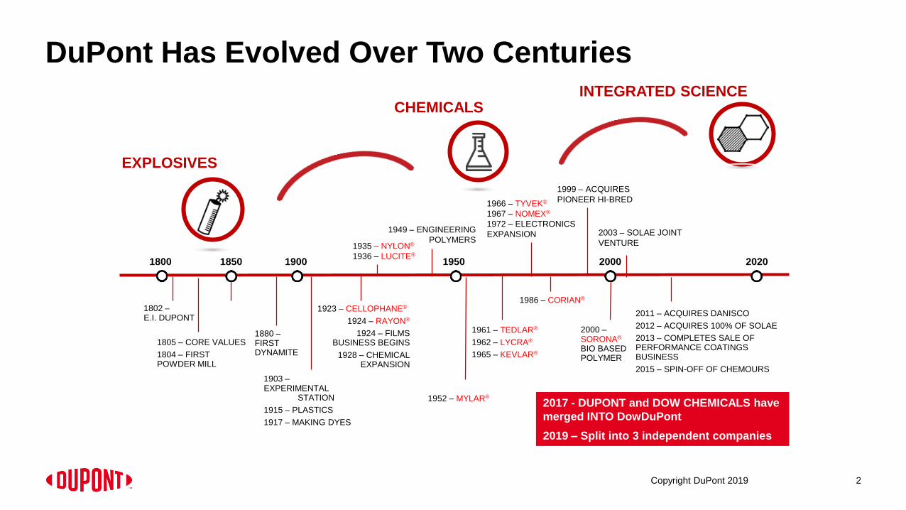
DuPont Has Evolved Over Two Centuries
2
EXPLOSIVES
CHEMICALSINTEGRATED SCIENCE
1935 – NYLON®
1936 – LUCITE®
1903 –EXPERIMENTAL
STATION
1915 – PLASTICS
1917 – MAKING DYES
1880 –FIRST DYNAMITE
1802 –E.I. DUPONT
1961 – TEDLAR®
1962 – LYCRA®
1965 – KEVLAR®
1952 – MYLAR®
1923 – CELLOPHANE®
1924 – RAYON®
1924 – FILMS BUSINESS BEGINS
1928 – CHEMICAL EXPANSION
202020001950190018501800
1949 – ENGINEERING
POLYMERS
1986 – CORIAN®
2003 – SOLAE JOINT
VENTURE
1966 – TYVEK®
1967 – NOMEX®
1972 – ELECTRONICS
EXPANSION
2000 –SORONA®
BIO BASED POLYMER
1805 – CORE VALUES
1804 – FIRST POWDER MILL
1999 – ACQUIRES
PIONEER HI-BRED
2011 – ACQUIRES DANISCO
2012 – ACQUIRES 100% OF SOLAE
2013 – COMPLETES SALE OF PERFORMANCE COATINGS BUSINESS
2015 – SPIN-OFF OF CHEMOURS
2017 - DUPONT and DOW CHEMICALS have
merged INTO DowDuPont
2019 – Split into 3 independent companies
Copyright DuPont 2019

Electronics & Imaging Advanced MaterialsBusiness Development: Science + Market Needs → Innovation
3Copyright DuPont 2019

Products:
High & Low
Temperature
Screen Printable
Pastes:
• Conductors
• Resistors
• Dielectrics
Core
Technologies:
Fine Powders
Ceramic Science
Glass Science
Coating Technology
Polymer Science
Photopolymer
Technology
Dispersions
Rheology
Tape Casting
Majo
r T
rad
itio
na
l A
pp
lic
ati
on
s
Power SupplyBio-Medical
Automotive
Photovoltaic
MTS
EL
RFID
Over 50 years of experience in the development, manufacture
and sale of specialized “Thick Film Compositions” (Pastes / Inks)
for the Printed Electronics Industry
Microcircuit Materials Traditional Business
Copyright DuPont 2019 4

Automotive Interiors History – Past
Copyright DuPont 2019 5

Automotive Interiors History – Recent
Copyright DuPont 2019 6

Automotive Interiors History – Present
Copyright DuPont 2019 7
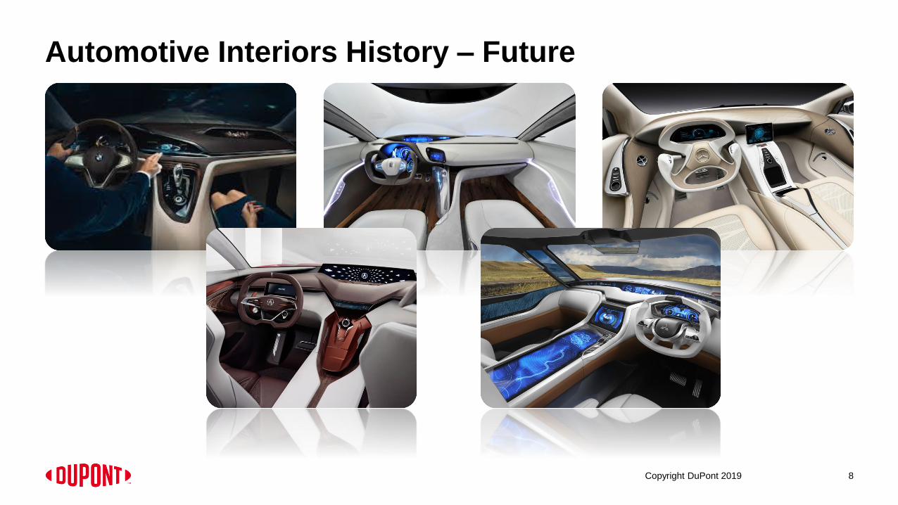
Automotive Interiors History – Future
Copyright DuPont 2019 8

Aesthetical, Intelligent 3D Surfaces
What if I could
encapsulate
intelligence and
functionality directly
into 3D surfaces?
Actually there is however a major limitation:
Copyright DuPont 2019 9
PCBs are flat & rigid
constraining the
design options and
the intelligent function
effectiveness…

Example: HMI Control Panel
Traditional Design Example
Surface plastics (Foil visual
finish and molded plastic)
Flex for capacitive switch
Light pipes
Full width rigid PCB
Design Properties
• Assembly depth: 25+ mm
• Numerous components
• Multiple manual assembly processes
• Complex electrical connections
• Mature technologies
Copyright DuPont 2019 10
Surface Encapsulated Design Example
Foil with visual finish
Printed circuitry, SMD
LEDs and ICs on IML foil
Injection-molded plastic
Design Properties
• Wall thickness: ~3 mm
• 50-70% weight reduction
• Sensors in surface structure
• Environmentally-protected electronics
• Consolidated electrical connections
• Single-component solution
Courtesy of TactoTek

Example: Overhead Console
Copyright DuPont 2019 11
Conventional assembly IME version Differences
Weight 650 g 150 g 77% lighter
Assembly depth 45 mm 3 mm (un-form) 93% less depth
Mechanical parts 64 parts 2 96% less parts
PCBA size (*DP estimate) 10 x 4 cm 10 x 3 cm 25% smaller area
Before (mechanical button) After (capacitive touch)
Source: Tactotek

Intelligent Surfaces Potential
Integration of:
• Electronic circuits: Electrical
connections, shielding, etc…
• Interfaces: Capacitive switches,
curved touch surfaces etc…
• Sensors: Antennas, proximity
and gesture detectors, etc…
• Electronic components: LEDs,
ICs, etc...
• Screens: OLEDs…?
Copyright DuPont 2019 12

The Ready To Use Solution
The Ready To Use Solution
Copyright DuPont 2019 13
Introducing “In Mold Electronics”
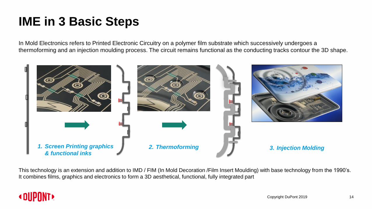
1. Screen Printing graphics
& functional inks3. Injection Molding2. Thermoforming
This technology is an extension and addition to IMD / FIM (In Mold Decoration /Film Insert Moulding) with base technology from the 1990’s.
It combines films, graphics and electronics to form a 3D aesthetical, functional, fully integrated part
IME in 3 Basic Steps
In Mold Electronics refers to Printed Electronic Circuitry on a polymer film substrate which successively undergoes a
thermoforming and an injection moulding process. The circuit remains functional as the conducting tracks contour the 3D shape.
Copyright DuPont 2019 14
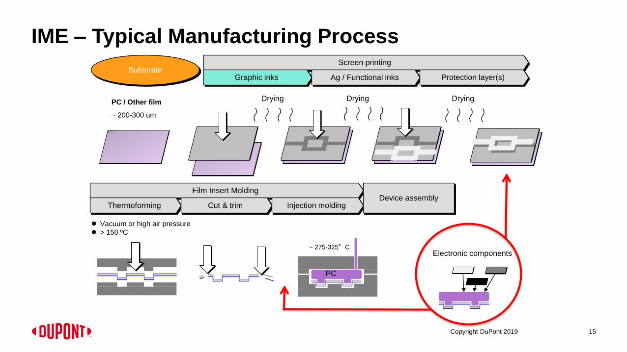
Screen printing
Graphic inks Ag / Functional inks Protection layer(s)Substrate
Film Insert Molding
Thermoforming Cut & trim Injection moldingDevice assembly
PC / Other film
~ 200-300 um
⚫ Vacuum or high air pressure
⚫ > 150 ºC
Electronic components
PC
Drying
~ 275-325°C
Drying Drying
IME – Typical Manufacturing Process
Copyright DuPont 2019 15
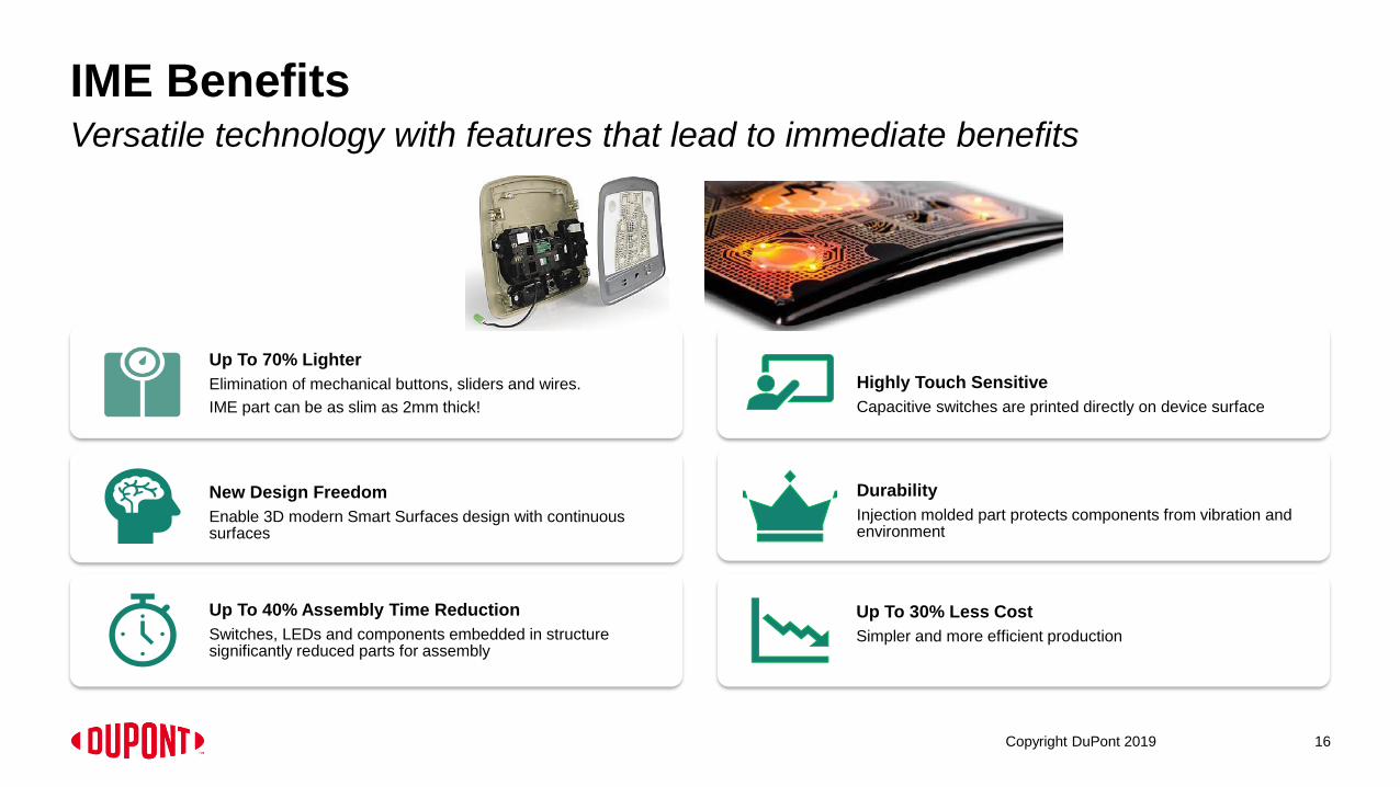
IME BenefitsVersatile technology with features that lead to immediate benefits
Copyright DuPont 2019 16
Up To 70% Lighter
Elimination of mechanical buttons, sliders and wires.
IME part can be as slim as 2mm thick!
New Design Freedom
Enable 3D modern Smart Surfaces design with continuous surfaces
Up To 40% Assembly Time Reduction
Switches, LEDs and components embedded in structure significantly reduced parts for assembly
Highly Touch Sensitive
Capacitive switches are printed directly on device surface
Durability
Injection molded part protects components from vibration and environment
Up To 30% Less Cost
Simpler and more efficient production

Enabling Technology
Through the
developments of
new, specially
formulated
functional inks
Conventional printed
electronics Ag Paste
ME602 thermoformable
silver ink
Enabling TechnologyWhy has this not been possible before and how is this achieved now?
Copyright DuPont 2019 17

Paste / Inks ConstituentsKey elements of a polymeric IME paste composition
Copyright DuPont 2019 18
Polymer
Filler
Solvent
Elastic / Stretchable
Good adhesion to PC
Withstands high temperatures
Solubilises the polymer
Good screen print properties
Compatible with PC & graphic inks
Conductor: Ag, Carbon, etc.
Dielectrics: different for under / over print, cross-over, etc.
IME functional ink
• Compatibility with substrates / graphic inks / and among
DuPont IME ink portfolio
• Balance of viscosity, good printing properties
• Balance for conductivity & ability to stretch
• Good adhesion and temperature resistance to withstand
“wash out” during injection moulding process

Conductive Adhesive
ME902 - For attach component, thermoformable, good
adhesion
Silver Conductor ME602 - PC friendly & for over-printing on graphic inks
ME603 - PC compatible & improved Ag show-through
ME101 - For RFID Antenna, NFC enable (reduced elongation)
IME Product Portfolio – Dielectrics
Copyright DuPont 2019 19
Transparent Conductor
ME801 - Good conductivity, high light transmission >90%
Carbon Conductor
ME201 - Overprint for connectors & to inhibit Ag
migration

Crossover Dielectric
ME778 - Reduced pinhole, stable BDV at elongation
ME779 - Wide process window (oven or belt drier)
Protection Encapsulant
ME772 - White Over-print protection – solvent based
ME780 - Clear Over-print protection – solvent based, good abrasion
with UV protection
IME Product Portfolio – Dielectrics
Copyright DuPont 2019 20

DuPont IME Active Collaborations
To provide an IME
solution to the Industry -
from paste to final
functional device - we
know there are
challenges related to
materials and processes:
Collaboration with
technology leaders and
specialized innovators
is therefore essential
Copyright DuPont 2019 21
Printing
• Pröll - Graphic Inks
Thermoforming
• Niebling - High Pressure
Solutions & Know-How
• Various companies -
specializing in IME
Application Development Resource
• Holst Centre – Hybrid Printed Electronics cluster
WP7 Platform (In Mould Electronics)
• Versatile technology
• In Mold Electronics is ideally suited to quickly develop “intelligent surface” solutions by fitting existing IMD / FIM
products and processes
IME – Summary / Conclusions
Copyright DuPont 2019 22
• Novel dedicated ink technology and complete suite of materials
• New functional ink chemistries for conductors, dielectrics, carbons and adhesives complying with the typical IMD /
FIM substrates, stretching and thermal / mechanical process conditions
• Robust and reliable technology and products
• Proved environmental test performance and thermal cycling resistance
• Ongoing technical work
• New generation of improved conductors and dielectrics
• Layers stack up design
• Generation of additional reliability data
© 2019 DuPont. All rights reserved. DuPont™, the DuPont Oval Logo, and all trademarks and service marks denoted with ™, ℠ or ® are owned by affiliates of DuPont de Nemours, Inc. unless otherwise noted. Nothing contained herein shall be construed as a representation that any recommendations, use or resale of the product or process described herein is permitted and complies
with the rules or regulations of any countries, regions, localities, etc., or does not infringe upon patents or other intellectual property rights of third parties.
The information provided herein is based on data DuPont believes to be reliable, to the best of its knowledge and is provided at the request of and without charge to our customers. Accordingly,DuPont does not guarantee or warrant such information and assumes no liability for its use. If this product literature is translated, the original English version will control and DuPont hereby
disclaims responsibility for any errors caused by translation. This document is subject to change without further notice.