
Focused ion beam and scanning electron microscopy for 3D...
14
MRS Bulletin Formatted w/Refs Kotula/Apr14 1 Focused ion beam and scanning electron microscopy for 3D materials characterization Paul G. Kotula, Gregory S. Rohrer, and Michael P. Marsh In this article, we review focused ion beam serial sectioning microscopy paired with analytical techniques, such as electron backscatter diffraction or x-ray energy-dispersive x-ray spectrometry, to study materials chemistry and structure in three dimensions. These three-dimensional microanalytical approaches have been greatly extended due to advances in software for both microscope control and data interpretation. Samples imaged with these techniques reveal structural features of materials that can be quantitatively characterized with rich chemical and crystallographic detail. We review these technological advances and the application areas that are benefitting. We also consider the challenges that remain for data collection, data processing, and visualization, which collectively limit the scale of these investigations. Further, we discuss recent innovations in quantitative analyses and numerical modeling that are being applied to microstructures illuminated by these techniques. Taxonomy: scanning electron microscopy (SEM); chemical composition; crystallographic structure; ion solid interactions. Introduction A focused ion beam (FIB) system coupled with a scanning electron microscope (SEM) on the same platform, often referred to as an FIB-SEM microscope, is a powerful combination for 3D microstructural analysis. The FIB is used serially to remove layers of material, while the electron beam is used to illuminate the freshly exposed surface. While early FIB-SEM imaging yielded 3D data stacks from measured electron signals (secondary electron or backscattered electron), more recent developments have integrated diffraction and x-ray spectroscopy with 3D FIB-SEM imaging. This article briefly reviews recent developments in acquisition and analysis of 3D FIB-SEM electron backscatter diffraction (EBSD) and x-ray microanalysis. A related review was recently
Transcript of Focused ion beam and scanning electron microscopy for 3D...

MRS Bulletin Formatted w/Refs Kotula/Apr14
1
Focused ion beam and scanning electron microscopy for 3D materials
characterization
Paul G. Kotula, Gregory S. Rohrer, and Michael P. Marsh
In this article, we review focused ion beam serial sectioning microscopy
paired with analytical techniques, such as electron backscatter diffraction or x-ray
energy-dispersive x-ray spectrometry, to study materials chemistry and structure
in three dimensions. These three-dimensional microanalytical approaches have
been greatly extended due to advances in software for both microscope control
and data interpretation. Samples imaged with these techniques reveal structural
features of materials that can be quantitatively characterized with rich chemical
and crystallographic detail. We review these technological advances and the
application areas that are benefitting. We also consider the challenges that remain
for data collection, data processing, and visualization, which collectively limit the
scale of these investigations. Further, we discuss recent innovations in
quantitative analyses and numerical modeling that are being applied to
microstructures illuminated by these techniques.
Taxonomy: scanning electron microscopy (SEM); chemical composition; crystallographic structure; ion solid interactions.
Introduction
A focused ion beam (FIB) system coupled with a scanning electron
microscope (SEM) on the same platform, often referred to as an FIB-SEM
microscope, is a powerful combination for 3D microstructural analysis. The FIB
is used serially to remove layers of material, while the electron beam is used to
illuminate the freshly exposed surface. While early FIB-SEM imaging yielded 3D
data stacks from measured electron signals (secondary electron or backscattered
electron), more recent developments have integrated diffraction and x-ray
spectroscopy with 3D FIB-SEM imaging. This article briefly reviews recent
developments in acquisition and analysis of 3D FIB-SEM electron backscatter
diffraction (EBSD) and x-ray microanalysis. A related review was recently
MRS Bulletin Formatted w/Refs Kotula/Apr14
2
published by Holzer and Cantoni,1 and the interested reader is directed there for
more details on imaging and microanalytical developments.
Three-dimensional orientation mapping
Automated electron backscatter diffraction, which makes it possible to
accumulate a map of crystal orientations on a surface, has had a transformative
effect on the study of grain boundaries in polycrystals. It is currently possible to
measure several hundred orientations per second, enabling the determination of
the shapes and orientations of thousands of grains in a reasonable amount of time.
However, EBSD reveals information only on near-surface crystallography. Three-
dimensional (3D) details extending beneath the surface requires serial sectioning
(sequentially removing layers of material).2,3 The experimental solution for serial
sectioning has been made possible by dual beam microscopes that contain both an
electron beam for EBSD mapping and an FIB for milling away layers of material.
Efforts to fully automate the sequence of orientation mapping and FIB milling
have obviated user intervention in the imaging cycle, enabling the collection of
large 3D orientation maps of materials from which statistical information can be
derived.4–10 For example, a 3D orientation map of a ferritic steel is shown in
Figure 1.
Three-dimensional orientation maps, compared to two-dimensional
images, occupy large banks of memory and are time consuming to measure. A
typical 3D map will take several days to measure, where the time demand scales
with the field of view and the number of parallel sections examined. In a
conventional FIB-SEM microscope, orientation mapping and milling require
comparable amounts of time. To balance the cost of the instrument time with the
desire to collect as much useful information as possible, it is important to consider
the choices for the spacing of the orientation points both within planes and
between planes. It has been found that the spacing between planes should be no
greater than 1/10th of the mean grain size, and the spacing of orientation points in
the plane should be equal to or less than the spacing between planes.10
Data processing is very important for the accurate calculation of
microstructural quantities. There are commercially available software solutions,

MRS Bulletin Formatted w/Refs Kotula/Apr14
3
such as Avizo,11 but they tend to emphasize structure rather than orientation and
images rather than statistics. For the processing of 3D orientation maps, one
capable platform is Dream.3D, developed by Groeber and Jackson.12 Dream.3D
uses another open source software package, ParaView,13 for interactive
visualization. As an example, the image in Figure 1 was created in Dream.3D and
displayed using ParaView.
One of the most statistically valuable methods to describe the
microstructure of a polycrystalline material is the grain boundary character
distribution (GBCD), which can be derived only from 3D orientation maps.14,15
The grain boundary character is specified by five parameters. For each pair of
neighboring grains, the misorientation between the two grains (given by
misorientation axis and a misorientation angle, which is a rotational around the
misorientation axis), and the orientation of planar interface between the two
grains (specified by a unit vector normal to the boundary [two angles]) are
recorded. It must be noted that the computation of grain boundary character is
highly sensitive to the alignment of sequential 2D orientation maps; a poor
alignment would give errant grain boundary positions, thereby giving incorrect
boundary plane orientations.
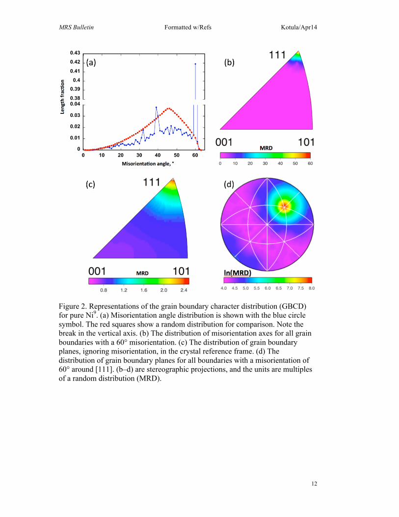
The results in Figure 2 show different components of a grain boundary
character distribution data obtained by 3D serial sectioning in the FIB. This
particular distribution is for high purity Ni9. Note that these data and many others
can be found at the Grain Boundary Data Archive, an online repository.16 The
distribution of grain boundary misorientation angles is shown in Figure 2a. The
peak at 60° corresponds to the Σ3 misorientation; this is a grain boundary with a
lattice misorientation of 60° around the [111] axis. The peak at 39° corresponds
to the Σ9 boundary; this is a grain boundary with a 39° misorientation around the
[110] axis. The distribution of grain boundary planes is presented in Figure 2b and
shows a preference for (111) planes. The distribution of misorientation axes for
grain boundaries with a 60° misorientation angle is shown in Figure 2c. The
strong peak at [111] demonstrates that these are Σ3 boundaries, which have a
misorientation of 60° about [111]. Finally, the distribution of grain boundary

MRS Bulletin Formatted w/Refs Kotula/Apr14
4
planes at the Σ3 misorientation is shown in Figure 2d. The maximum is at the
(111) position, and this corresponds to the coherent twin grain boundary.
One valuable application of the 3D data is as input to numerical
simulations of properties.17 Material properties can be simulated based on models
that are ensembles of microstructure statistics, but there is no substitute for
building a model directly from the empirically observed microstructure. As an
example of numerical modeling of a polycrystal, the 3D orientation map on a
regular grid can be used as input into simulations of mechanical response using
the fast Fourier transform method to determine the plastic response of a material
to mechanical loads.18 This method has been used to identify microstructural “hot
spots” or stress concentrations in Ni microstructures.
Applications like Dream.3D and Avizo can be used to create meshed
models of microstructures that can then be exported in formats that are accepted
by standard finite element model simulations. Ghosh and coworkers have outlined
the challenges for constructing a simulation-ready mesh specifically from 3D
orientation maps.19
Numerical modeling can be computationally demanding. Lewis and
coworkers describe shortcuts that can extend the scale of the system that can be
studied.20 Usually, these shortcuts involve reducing the complexity of the model
by, for example, using adaptive mesh refinement methods or simply reducing the
model domain down to a representative volume. As evolving imaging methods
deliver larger 3D volumes at higher resolutions, image-derived modeling will
continue to demand greater computing resources.
Three-dimensional x-ray microanalysis
Much like EBSD, conventional x-ray energy dispersive spectroscopy
(XEDS) microanalysis interrogates only the surface of a sample. Quite often,
however, a 2D chemical map is not sufficient to answer a scientific question, and,
therefore, methods for 3D analysis are needed. The first 3D measurement using
electron excited x-rays in an SEM was performed with mechanical sectioning
followed by acquisition of pre-selected x-ray maps.21

MRS Bulletin Formatted w/Refs Kotula/Apr14
5
The first measurements of 3D elemental distributions with an FIB-SEM
equipped with an x-ray detector were done without the benefit of automation,
with the operator serially milling layers with the FIB and scanning those layers
with the SEM as an x-ray detector was used to acquire full spectral images22–24
The analytical geometry developed in that work is shown in Figure 3 for the
example of the analysis of a copper silver eutectic alloy. Figure 3a is a secondary-
electron image taken from the perspective of the x-ray detector showing the
trenches milled to first expose the analysis surface to the electron beam, and
second, a trench to the right that removes sample material that would otherwise
obscure x-rays from reaching the detector. While this image shows some material-
specific contrast, it is not definitive of the chemical phases in the sample. Figure
3b is a schematic of the analysis geometry. These data were acquired manually in
about one day’s time and consisted of 10 serial sections, each with a full spectrum
at every pixel. The technique of 3D XEDS was successfully automated using a
combination of the FIB manufacturer’s scripting and custom scripting software to
control the XEDS software,25 and commercial integration of FIB-SEM and XEDS
has been available since 2011.26
Performing microanalysis in a trench is far from ideal, as both
backscattered electrons and x-rays can excite x-rays from areas far from the
analysis surface. This has been overcome by using a micromanipulator in the FIB
to remove a volume of material and place it on a support.27 Although this method
takes longer, the resulting volume of material removed from the trench can then
be sectioned and analyzed without the spurious background signal. In many cases
though, an analyzed geometry with a trench is both faster and easier while
allowing for the most common qualitative analyses.
Ultimately though, what limits the microanalytical spatial resolution is not
the surrounding material (the trench for example) or the slice thickness. Rather, it
is the energy of the incident electrons on the analysis face and the average atomic
number of the target material. The incident electron beam generates x-rays from a
volume of material, thus making this technique near-surface sensitive. With an
electron-energy of 15 keV, the interaction volume for the generation of x-rays for

MRS Bulletin Formatted w/Refs Kotula/Apr14
6
an aluminum target would be about 3 µm, for titanium it would be about 2 µm,
and for copper it would be about 1 µm. For platinum, however, it would be about
100 nm. We can improve this, especially for low atomic number targets, by
decreasing the incident electron voltage but at the expense of efficiently exciting
only lower energy x-ray transitions. The resulting emission bands tend to overlap
with each other for many elements. At very low energy though, we come to the
limit of current XEDS systems where excited transitions are not detectable by the
current x-ray detectors. As a rule of thumb, an electron beam voltage of two times
the ionization energy for a transition of a target material is desirable.
A 3D x-ray spectral image (termed tomographic spectral image)24 contains
a full x-ray spectrum in each voxel in a 3D array. A significant challenge then is
how to comprehensively analyze what can consist of billions of data elements
(number of voxels times number of x-ray energy channels) without a priori
knowledge of the material composition. Multivariate statistical analysis (MSA) is
key to interpreting these high-dimensional data; by reducing the large number of
initial variables (typically the spectral channels) into a smaller number of more
discriminating variables, MSA yields physically interpretable factors.24,28,29 The
factors consist of corresponding component images and spectral shapes.
As an example of the use of lower accelerating voltages to improve the
spatial resolution of 3D XEDS, 5 keV was used to analyze a localized corrosion
event22–24 on a gold and nickel plated copper specimen where the initial elements
of interest were gold (Au-M 2.123 keV), nickel (Ni-Lα 0.852 keV), and copper
(Cu-Lα 0.930 keV), plus corrosion products likely including sulfur (S-K 2.308
keV). Unexpectedly, in this case, Si and O were found using advanced data
analysis methods.24 Rather than choosing elements in advance for data collection,
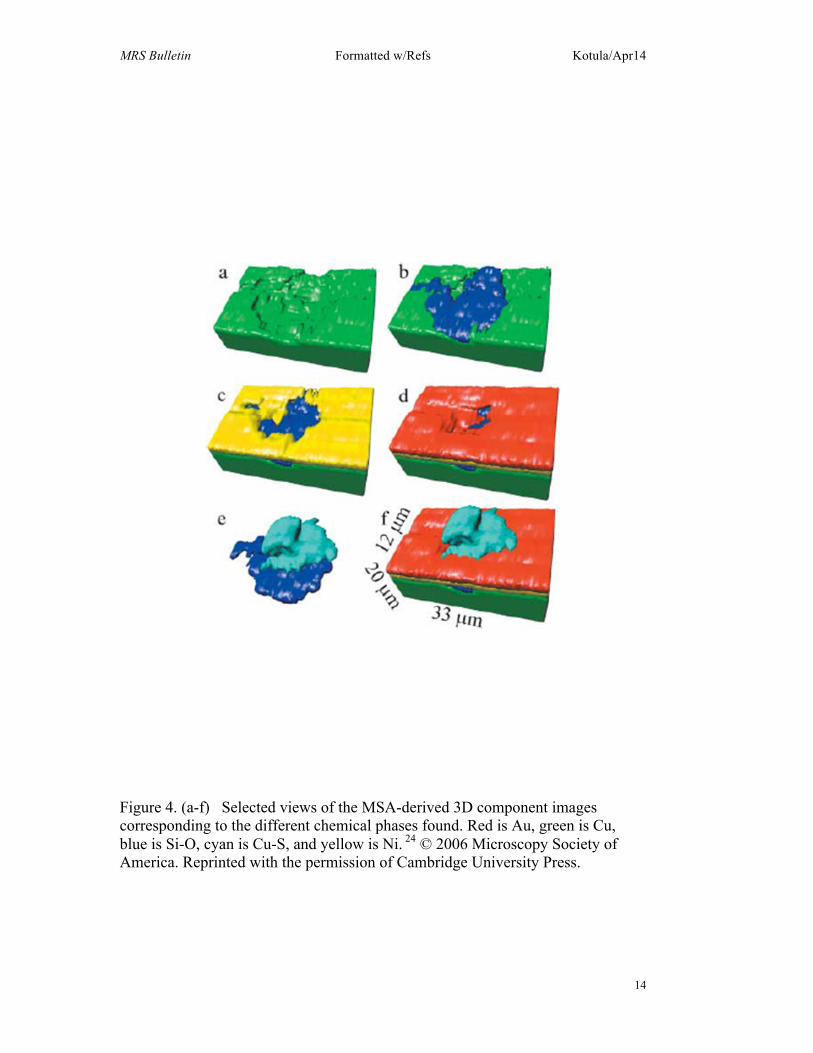
the full spectral image data were collected for retrospective analysis. Figures 4a-f
show the component images from the MSA analysis of the tomographic spectral
image rendered in 3D where Au is red, Cu is green, Si-O is blue, Cu-S is magenta
and Ni is yellow.24 The Si-O contaminant on the Cu substrate came from a grit-
blasting process step intended to roughen the substrate to improve adhesion of the
electrodeposited Ni and Au layers with the Au in particular used prevent
MRS Bulletin Formatted w/Refs Kotula/Apr14
7
corrosion. The presence of the Si-O created a defect in the Ni plating which the
Au only partially covered leaving a path for corrosion to occur.
In conventional processing, maps corresponding to expected elements are
visualized with 3D rendering software. One challenge though is the fact that with
low incident beam energies, many x-ray lines from different elements overlap
(e.g., Fe-L and F-K), which is referred to as pathological overlap. If we acquire
the full spectral data at each 3D volume element (voxel) though (the standard
approach now), we can apply more advanced data processing methods that require
no a priori knowledge of the elements that may be present,28 and can thus
effectively be deconvolved for many such pathological overlaps.
Three-dimensional elemental maps can be used as models for numerical
simulations, but there are no unique requirements as there are with 3D orientation
maps. Whereas conventional FIB-SEM electron imaging experiments must be
segmented (identifying what greyscale values correspond to what elements), a
clean 3D elemental map requires no segmentation. Generally preferable to
conventional FIB-SEM electron images, XEDS maps definitively measure the
chemistry at every position in the 3D model. But in some cases, this may not be
strictly necessary. Iwai and coworkers have shown30 that the secondary electron
(SE) contrast is sufficient to differentiate the materials in every slice of a 3D data
set of a solid oxide fuel cell anode. An XEDS map of a single representative slice
is sufficient to calibrate the greyscale interpretation for all of the slices in the 3D
SE map. Their 3D model was then subjected to lattice Boltzmann simulation of
ionic diffusion in the measured microstructure.30 Despite the success of this study,
grayscale resolution in the SE signal is far less characteristic than chemical
mapping by XEDS. Alternatively, it is possible to collect electron images from
finely spaced slices and then collect x-ray spectral images from larger depth
intervals (e.g., every fifth or tenth slice).26 In this way, data acquisition can be
optimized for post-processing at the best spatial resolution of the respective
techniques.
Remaining challenges and future developments

MRS Bulletin Formatted w/Refs Kotula/Apr14
8
The scale of these 3D microstructural analyses studies is limited by the
milling rate. Since the liquid-metal ion source in Ga FIB columns is physically
very small, it is difficult to obtain a large Ga beam current commensurate with the
relatively large serial section thicknesses useful for 3D microanalysis and thus
larger volume removal. Recent developments in gaseous plasma sources31 have
raised the possibility of a plasma FIB-SEM. The volumes of material that could
then be analyzed would increase significantly so that operators could realistically
perform serial sectioning experiments at depths on the order of 500 µm.
Large datasets can be computationally taxing. Data interpretation and
microstructural characterization is possible with current hardware, but many
desirable simulations are not tractable. This will be addressed only when
numerical simulation engines are more highly optimized or when more
computational power is applied to the problems.
Future advances in 3D XEDS microanalysis will involve the use of higher
solid angle silicon-drift energy-dispersive x-ray detectors (SDDs) to shorten the
time required to collect the x-ray data. Free from liquid nitrogen cooling, these
SDDs can be fashioned into custom geometries that can be positioned closer to
the specimen or subtend larger solid angles.32,33
Summary
Until recently, 3D microanalysis experiments were possible only by labor-
intensive manual approaches, and often there was no user-friendly software for
data interpretation. Advances in FIB-SEM instrument control software have
greatly simplified data collection for both 3D orientation maps and 3D elemental
mapping experiments for a variety of application areas. Third party and vendor
software for 3D orientation mapping interpretation has made it possible to
thoroughly characterize crystallographic microstructures and even numerically
simulate physical properties of polycrystalline materials such as ceramics17 and
minerals.34 Three-dimensional chemical mapping reveals the makeup of samples
of the materials sciences,24,25,35 and even life-science specimens;37 the former has
benefited strongly from MSA techniques for dealing with high-dimensional

MRS Bulletin Formatted w/Refs Kotula/Apr14
9
spectral data. The scale of specimens studied with these techniques is likely to
grow, especially when FIB milling rates are accelerated by new technologies.
Acknowledgments
Sandia is a multiprogram laboratory operated by Sandia Corporation, a
Lockheed Martin Company, for the United States Department of Energy (DOE)
under contract DE-AC0494AL85000. P. K. acknowledges Michael Rye at Sandia
for helping with manual serial sectioning and 3D XEDS acquisition. G.S.R.
acknowledges financial support from the ONR-MURI under Grant No. N00014–
11–1-0678 and the MRSEC program of the National Science Foundation under
Award DMR-0520425.
References
1. L. Holzer, M. Cantoni, Review of FIB Tomography in Nanofabrication Using Focused Ion and Electron Beams: Principles and Applications (Oxford University Press, Oxford, UK, 2012), chap. 11.
2. D.J. Rowenhorst, A.C. Lewis, G. Spanos, Acta Mater. 58, 5511 (2010).
3. D.M. Saylor, A. Morawiec, G.S. Rohrer, Acta Mater. 51, 3663 (2003).
4. H. Beladi, G.S. Rohrer, Acta Mater. 61, 1404 (2013).
5. S.J. Dillon, L. Helmick, H.M Miller, L. Wilson, R. Gemman, R.V. Petrova, K. Barmak, G.S. Rohrer, P.A. Salvador , J. Am. Ceram. Soc. 94, 4045 (2011).
6. S.J. Dillon, G.S. Rohrer, J. Am. Ceram. Soc. 92, 1580 (2009).
7. M.A. Groeber, B.K. Haley, M.D. Uchic, D.M. Dimiduk, S. Ghosh, Mater. Charact. 57, 259 (2006).
8. A. Khorashadizadeh, D. Raabe, M. Winning, R. Pippan, Adv. Eng. Mater. 13, 237 (2011).
9. J. Li, S.J. Dillon, G.S. Rohrer, Acta Mater. 57, 4304 (2009).
10. G.S. Rohrer, J. Li, S. Lee, A.D. Rollett, M. Groeber, M.D. Uchic, Mater. Sci. Technol. 26, 661 (2010).
11. FEI Visualization Sciences Group, Avizo (2013); http://www.vsg3d.com/avizo/overview.
12. M.A. Groeber, M.A. Jackson, Integr. Mater. Manuf. Innov. in press, (2014).

MRS Bulletin Formatted w/Refs Kotula/Apr14
10
13. Kitware, ParaView (2013); http://www.paraview.org/.
14. G.S. Rohrer, J. Am. Ceram. Soc. 94, 633 (2011).
15. G.S. Rohrer, D. M. Saylor, B. El Dasher, B. L. Adams, A. D. Rollett,
P. Wynblatt, Z. Metallkd. 95, 197 (2004).
16. G. Rohrer, Grain Boundary Data Archive (2013); http://mimp.mems.cmu.edu/~gr20/Grain_Boundary_Data_Archive.
17. S.-B. Lee, T.S. Key, Z. Liang, R.E. García, S. Wang, X. Tricoche, G.S. Rohrer, Y. Saito, C. Ito, T. Tani, J. Eur. Ceram. Soc. 33, 313 (2013).
18. A. Rollett, R A Lebensohn, M Groeber, Y Choi, J Li, G S Rohrer, Model. Simul. Mater. Sci. Eng. 18, 074005 (2010).
19. S. Ghosh, Y. Bhandari, M. Groeber, Comput. Aided Des. 40 (3), 293 (2008).
20. A.C. Lewis,S.M. Qidwai, M. Jackson, A.B. Geltmacher, JOM 63 (3), 35 (2011).
21. R. Marschallinger, Scanning 20, 65 (1998).
22. P.G. Kotula, M.R. Keenan, J.R. Michael, Microsc. Microanal. 9 (Suppl. 2), 1004 (2003).
23. P.G. Kotula, M.R. Keenan, J.R. Michael, Microsc. Microanal. 10 (Suppl. 2), 1132 (2004).
24. P.G. Kotula, M.R. Keenan, J.R. Michael, Microsc. Microanal. 12, 36–48 (2006).
25. M. Schaffer, J. Wagner, B. Schaffer, M. Schmied, H. Mulders, Ultramicroscopy 107, 587 (2007).
26. Oxford Instruments plc, Automated 3D XEDS FIB integration; http://www.oxford-instruments.com/products/microanalysis/energy-dispersive-x-ray-systems-eds-edx/eds-for-sem/3d-eds-analysis.
27. M. Schaffer, J Wagner, Microchim. Acta 161, 421 (2008).
28. P.G. Kotula, M.R. Keenan, J.R. Michael, Microsc. Microanal. 9, 1 (2003).
29. P.G. Kotula, M.H. Van Benthem, N.R. Sorensen, IEEE Statistical Signal Processing Workshop (SSP) (2012), pp. 672–675.

MRS Bulletin Formatted w/Refs Kotula/Apr14
11
30. H. Iwai, N. Shikazonob, T. Matsuic, H. Teshimab, M. Kishimotoa, R. Kishidac, D. Hayashia, K. Matsuzakib, D. Kannob, M. Saitoa, H. Muroyamac, K. Eguchic, N. Kasagib, H. Yoshida, J. Power Sources 195 (4), 955 (2010).
31. N.S. Smith, W.P. Skoczylas, S.M. Kellogg, D.E. Kinion, P.P. Tesch, O. Sutherland, A. Aanesland, R.W. Boswell, J. Vac. Sci. Technol. B 24, 2902 (2006).
32. B.L. Doyle, D.S. Walsh, P.G. Kotula, P. Rossi, T. Schulein, M. Rohde, X-Ray Spectrom. 34 (4), 279 (2005).
33. P.G. Kotula, J.R. Michael, M. Rohde, Microsc. Microanal. 14 (Suppl. 2) 116 (2008).
34. V. Shushakova, E.R. Fuller Jr., F. Heidelbach, D. Mainprice, S. Siegesmund, Environ. Earth Sci. 69 (4), 1281 (2013).
35. R.D. Holbrook, J.M. Davis, K.C.K. Scott, C. Szakal, J. Microsc. 246, 143 (2012).
36. K. Scott, N.W.M. Ritchie, J. Microsc. 233, 331 (2009).
Figures
Figure 1. Reconstructed serial sections of electron backscatter diffraction data for a ferritic steel. The volume consists of 68 parallel layers. The colors are the orientations referred to as the normal direction. 33
MRS Bulletin Formatted w/Refs Kotula/Apr14
12
Figure 2. Representations of the grain boundary character distribution (GBCD) for pure Ni9. (a) Misorientation angle distribution is shown with the blue circle symbol. The red squares show a random distribution for comparison. Note the break in the vertical axis. (b) The distribution of misorientation axes for all grain boundaries with a 60° misorientation. (c) The distribution of grain boundary planes, ignoring misorientation, in the crystal reference frame. (d) The distribution of grain boundary planes for all boundaries with a misorientation of 60° around [111]. (b–d) are stereographic projections, and the units are multiples of a random distribution (MRD).

MRS Bulletin Formatted w/Refs Kotula/Apr14
13
Figure 3.
Figure 3. a: Secondary-electron image showing the trenches, protective Pt layer and fiducial (reference) markerstaken to approximate the view of analysis surface seen by the X-ray spectrometer. b: Schematic of the analysis geometry with (1) first stair-step trench, (2) second stair-step trench, and (3) fiducial markers.24 © 2006 Microscopy Society of America. Reprinted with the permission of Cambridge University Press.
MRS Bulletin Formatted w/Refs Kotula/Apr14
14
Figure 4. (a-f) Selected views of the MSA-derived 3D component images corresponding to the different chemical phases found. Red is Au, green is Cu, blue is Si-O, cyan is Cu-S, and yellow is Ni. 24 © 2006 Microscopy Society of America. Reprinted with the permission of Cambridge University Press.


