FM25V02A, 256-Kbit (32K × 8) Serial (SPI) F-RAM
23
FM25V02A 256-Kbit (32K × 8) Serial (SPI) F-RAM Cypress Semiconductor Corporation • 198 Champion Court • San Jose, CA 95134-1709 • 408-943-2600 Document Number: 001-90865 Rev. *G Revised September 27, 2016 256-Kbit (32K × 8) Serial (SPI) F-RAM Features ■ 256-Kbit ferroelectric random access memory (F-RAM) logically organized as 32K × 8 ❐ High-endurance 100 trillion (10 14 ) read/writes ❐ 151-year data retention (See the Data Retention and Endurance table) ❐ NoDelay™ writes ❐ Advanced high-reliability ferroelectric process ■ Very fast serial peripheral interface (SPI) ❐ Up to 40-MHz frequency ❐ Direct hardware replacement for serial flash and EEPROM ❐ Supports SPI mode 0 (0, 0) and mode 3 (1, 1) ■ Sophisticated write-protection scheme ❐ Hardware protection using the Write Protect (WP ) pin ❐ Software protection using Write Disable instruction ❐ Software block protection for 1/4, 1/2, or entire array ■ Device ID ❐ Manufacturer ID and Product ID ■ Low power consumption ❐ 2.5-mA active current at 40 MHz ❐ 150-A standby current ❐ 8-A sleep mode current ■ Low-voltage operation: V DD = 2.0 V to 3.6 V ■ Industrial temperature: –40 C to +85 C ■ Packages ❐ 8-pin small outline integrated circuit (SOIC) package ❐ 8-pin dual flat no-leads (DFN) package ■ Restriction of hazardous substances (RoHS) compliant Functional Description The FM25V02A is a 256-Kbit nonvolatile memory employing an advanced ferroelectric process. An F-RAM is nonvolatile and performs reads and writes similar to a RAM. It provides reliable data retention for 151 years while eliminating the complexities, overhead, and system-level reliability problems caused by serial flash, EEPROM, and other nonvolatile memories. Unlike serial flash and EEPROM, the FM25V02A performs write operations at bus speed. No write delays are incurred. Data is written to the memory array immediately after each byte is successfully transferred to the device. The next bus cycle can commence without the need for data polling. In addition, the product offers substantial write endurance compared with other nonvolatile memories. The FM25V02A is capable of supporting 10 14 read/write cycles, or 100 million times more write cycles than EEPROM. These capabilities make the FM25V02A ideal for nonvolatile memory applications requiring frequent or rapid writes. Examples range from data logging, where the number of write cycles may be critical, to demanding industrial controls where the long write time of serial flash or EEPROM can cause data loss. The FM25V02A provides substantial benefits to users of serial EEPROM or flash as a hardware drop-in replacement. The FM25V02A uses the high-speed SPI bus, which enhances the high-speed write capability of F-RAM technology. The device incorporates a read-only Device ID that allows the host to determine the manufacturer, product density, and product revision. The device specifications are guaranteed over an industrial range of –40 C to +85 C. For a complete list of related resources, click here. Logic Block Diagram Instruction Decoder Clock Generator Control Logic Write Protect Instruction Register Address Register Counter 32 K x 8 F-RAM Array 15 Data I/ O Register 8 Nonvolatile Status Register 3 WP CS HOLD SCK SO SI
Transcript of FM25V02A, 256-Kbit (32K × 8) Serial (SPI) F-RAM

FM25V02A
256-Kbit (32K × 8) Serial (SPI) F-RAM
Cypress Semiconductor Corporation • 198 Champion Court • San Jose, CA 95134-1709 • 408-943-2600Document Number: 001-90865 Rev. *G Revised September 27, 2016
256-Kbit (32K × 8) Serial (SPI) F-RAM
Features
■ 256-Kbit ferroelectric random access memory (F-RAM)logically organized as 32K × 8 ❐ High-endurance 100 trillion (1014) read/writes ❐ 151-year data retention (See the Data Retention and
Endurance table)❐ NoDelay™ writes ❐ Advanced high-reliability ferroelectric process
■ Very fast serial peripheral interface (SPI)❐ Up to 40-MHz frequency ❐ Direct hardware replacement for serial flash and EEPROM❐ Supports SPI mode 0 (0, 0) and mode 3 (1, 1)
■ Sophisticated write-protection scheme❐ Hardware protection using the Write Protect (WP) pin❐ Software protection using Write Disable instruction❐ Software block protection for 1/4, 1/2, or entire array
■ Device ID❐ Manufacturer ID and Product ID
■ Low power consumption❐ 2.5-mA active current at 40 MHz❐ 150-A standby current❐ 8-A sleep mode current
■ Low-voltage operation: VDD = 2.0 V to 3.6 V
■ Industrial temperature: –40 C to +85 C
■ Packages❐ 8-pin small outline integrated circuit (SOIC) package ❐ 8-pin dual flat no-leads (DFN) package
■ Restriction of hazardous substances (RoHS) compliant
Functional Description
The FM25V02A is a 256-Kbit nonvolatile memory employing anadvanced ferroelectric process. An F-RAM is nonvolatile andperforms reads and writes similar to a RAM. It provides reliabledata retention for 151 years while eliminating the complexities,overhead, and system-level reliability problems caused by serialflash, EEPROM, and other nonvolatile memories.
Unlike serial flash and EEPROM, the FM25V02A performs writeoperations at bus speed. No write delays are incurred. Data iswritten to the memory array immediately after each byte issuccessfully transferred to the device. The next bus cycle cancommence without the need for data polling. In addition, theproduct offers substantial write endurance compared with othernonvolatile memories. The FM25V02A is capable of supporting1014 read/write cycles, or 100 million times more write cyclesthan EEPROM.
These capabilities make the FM25V02A ideal for nonvolatilememory applications requiring frequent or rapid writes.Examples range from data logging, where the number of writecycles may be critical, to demanding industrial controls where thelong write time of serial flash or EEPROM can cause data loss.
The FM25V02A provides substantial benefits to users of serialEEPROM or flash as a hardware drop-in replacement. TheFM25V02A uses the high-speed SPI bus, which enhances thehigh-speed write capability of F-RAM technology. The deviceincorporates a read-only Device ID that allows the host todetermine the manufacturer, product density, and productrevision. The device specifications are guaranteed over anindustrial range of –40 C to +85 C.
For a complete list of related resources, click here.
Logic Block Diagram
Instruction DecoderClock Generator
Control LogicWrite Protect
Instruction Register
Address Register Counter
32 K x 8 F-RAM Array
15
Data I/ O Register
8
Nonvolatile StatusRegister
3
WP
CS
HOLD
SCK
SOSI

FM25V02A
Document Number: 001-90865 Rev. *G Page 2 of 23
Contents
Pinouts .............................................................................. 3Pin Definitions .................................................................. 3Functional Overview ........................................................ 4Memory Architecture ........................................................ 4Serial Peripheral Interface - SPI Bus .............................. 4
SPI Overview ............................................................... 4SPI Modes ................................................................... 5Power-Up to First Access ............................................ 6Command Structure .................................................... 6WREN - Set Write Enable Latch ................................. 6WRDI - Reset Write Enable Latch ............................... 6
Status Register and Write Protection ............................. 7RDSR - Read Status Register ..................................... 7WRSR - Write Status Register .................................... 7
Memory Operation ............................................................ 8Write Operation ........................................................... 8Read Operation ........................................................... 8Fast Read Operation ................................................... 8HOLD Pin Operation ................................................. 10Sleep Mode ............................................................... 10Device ID ................................................................... 11Endurance ................................................................. 12
Maximum Ratings ........................................................... 13Operating Range ............................................................. 13DC Electrical Characteristics ........................................ 13Data Retention and Endurance ..................................... 14Capacitance .................................................................... 14Thermal Resistance ........................................................ 14AC Test Conditions ........................................................ 14AC Switching Characteristics ....................................... 15Power Cycle Timing ....................................................... 17Ordering Information ...................................................... 18
Ordering Code Definitions ......................................... 18Package Diagrams .......................................................... 19Acronyms ........................................................................ 21Document Conventions ................................................. 21
Units of Measure ....................................................... 21Document History Page ................................................. 22Sales, Solutions, and Legal Information ...................... 23
Worldwide Sales and Design Support ....................... 23Products .................................................................... 23PSoC®Solutions ....................................................... 23Cypress Developer Community ................................. 23Technical Support ..................................................... 23

FM25V02A
Document Number: 001-90865 Rev. *G Page 3 of 23
PinoutsFigure 1. 8-pin SOIC Pinout
Figure 2. 8-pin DFN Pinout
Pin Definitions
Pin Name I/O Type Description
SCK Input Serial Clock. All I/O activity is synchronized to the serial clock. Inputs are latched on the rising edgeand outputs occur on the falling edge. Because the device is synchronous, the clock frequency maybe any value between 0 and 40 MHz and may be interrupted at any time.
CS Input Chip Select. This active LOW input activates the device. When HIGH, the device enters thelow-power standby mode, ignores other inputs, and the output is tristated. When LOW, the deviceinternally activates the SCK signal. A falling edge on CS must occur before every opcode.
SI[1] Input Serial Input. All data is input to the device on this pin. The pin is sampled on the rising edge of SCKand is ignored at other times. It should always be driven to a valid logic level to meet IDD specifica-tions.
SO[1] Output Serial Output. This is the data output pin. It is driven during a read and remains tristated at all othertimes including when HOLD is LOW. Data transitions are driven on the falling edge of the serial clock.
WP Input Write Protect. This active LOW pin prevents write operation to the Status Register when WPEN isset to ‘1’. This is critical because other write protection features are controlled through the StatusRegister. A complete explanation of write protection is provided on Status Register and WriteProtection on page 7. This pin must be tied to VDD if not used.
HOLD Input HOLD Pin. The HOLD pin is used when the host CPU must interrupt a memory operation for anothertask. When HOLD is LOW, the current operation is suspended. The device ignores any transitionon SCK or CS. All transitions on HOLD must occur while SCK is LOW. This pin has a weak internalpull-up (refer to the RIN spec in DC Electrical Characteristics).
VSS Power supply Ground for the device. Must be connected to the ground of the system.
VDD Power supply Power supply input to the device.
EXPOSED PAD No connect The EXPOSED PAD on the bottom of 8-pin DFN package is not connected to the die. The EXPOSEDPAD should not be soldered on the PCB.
HOLD
SCK
1
2
3
4 5
CS 8
7
6
VDD
SI
SO Top Viewnot to scale
VSS
WP
SO
CS
VSS
WP
SI
VDD
SCK
HOLD
1
2
4 5
6
7
8
3
O
PADEXPOSED
Top Viewnot to scale
Note1. SI may be connected to SO for a single pin data interface.

FM25V02A
Document Number: 001-90865 Rev. *G Page 4 of 23
Functional Overview
The FM25V02A is a serial F-RAM memory. The memory array islogically organized as 32,768 × 8 bits and is accessed using anindustry-standard serial peripheral interface (SPI) bus. Thefunctional operation of the F-RAM is similar to serial flash andserial EEPROMs. The major difference between the FM25V02Aand a serial flash or EEPROM with the same pinout is theF-RAM's superior write performance, high endurance, and lowpower consumption.
Memory Architecture
When accessing the FM25V02A, the user addresses 32Klocations of eight data bits each. These eight data bits are shiftedin or out serially. The addresses are accessed using the SPIprotocol, which includes a chip select (to permit multiple deviceson the bus), an opcode, and a two-byte address. The upper bitof the address range is 'don't care' value. The complete addressof 15 bits specifies each byte address uniquely.
Most functions of the FM25V02A are either controlled by the SPIinterface or are handled by on-board circuitry. The access timefor the memory operation is essentially zero, beyond the timeneeded for the serial protocol. That is, the memory is read orwritten at the speed of the SPI bus. Unlike a serial flash orEEPROM, it is not necessary to poll the device for a readycondition because writes occur at bus speed. By the time a newbus transaction can be shifted into the device, a write operationis complete. This is explained in more detail in MemoryOperation on page 8.
Serial Peripheral Interface - SPI Bus
The FM25V02A is a SPI slave device and operates at speeds upto 40 MHz. This high-speed serial bus provides high-perfor-mance serial communication to a SPI master. Many commonmicrocontrollers have hardware SPI ports allowing a directinterface. It is quite simple to emulate the port using ordinary portpins for microcontrollers that do not. The FM25V02A operates inSPI Mode 0 and 3.
SPI Overview
The SPI is a four-pin interface with Chip Select (CS), Serial Input(SI), Serial Output (SO), and Serial Clock (SCK) pins.
The SPI is a synchronous serial interface, which uses clock anddata pins for memory access and supports multiple devices onthe data bus. A device on the SPI bus is activated using the CSpin.
The relationship between chip select, clock, and data is dictatedby the SPI mode. This device supports SPI modes 0 and 3. Inboth of these modes, data is clocked into the F-RAM on the risingedge of SCK starting from the first rising edge after CS goesactive.
The SPI protocol is controlled by opcodes. These opcodesspecify the commands from the bus master to the slave device.After CS is activated, the first byte transferred from the bus
master is the opcode. Following the opcode, any addresses anddata are then transferred. The CS must go inactive after anoperation is complete and before a new opcode can be issued.The commonly used terms in the SPI protocol are as follows:
SPI Master
The SPI master device controls the operations on a SPI bus. AnSPI bus may have only one master with one or more slavedevices. All the slaves share the same SPI bus lines and themaster may select any of the slave devices using the CS pin. Allof the operations must be initiated by the master activating aslave device by pulling the CS pin of the slave LOW. The masteralso generates the SCK and all the data transmission on SI andSO lines are synchronized with this clock.
SPI Slave
The SPI slave device is activated by the master through the ChipSelect line. A slave device gets the SCK as an input from the SPImaster and all the communication is synchronized with thisclock. An SPI slave never initiates a communication on the SPIbus and acts only on the instruction from the master.
The FM25V02A operates as an SPI slave and may share the SPIbus with other SPI slave devices.
Chip Select (CS)
To select any slave device, the master needs to pull down thecorresponding CS pin. Any instruction can be issued to a slavedevice only while the CS pin is LOW. When the device is notselected, data through the SI pin is ignored and the serial outputpin (SO) remains in a high-impedance state.
Note A new instruction must begin with the falling edge of CS.Therefore, only one opcode can be issued for each active ChipSelect cycle.
Serial Clock (SCK)
The serial clock is generated by the SPI master and thecommunication is synchronized with this clock after CS goesLOW.
The FM25V02A enables SPI modes 0 and 3 for data communi-cation. In both of these modes, the inputs are latched by theslave device on the rising edge of SCK and outputs are issuedon the falling edge. Therefore, the first rising edge of SCKsignifies the arrival of the first bit (MSB) of a SPI instruction onthe SI pin. Further, all data inputs and outputs are synchronizedwith SCK.
Data Transmission (SI/SO)
The SPI data bus consists of two lines, SI and SO, for serial datacommunication. SI is also referred to as Master Out Slave In(MOSI) and SO is referred to as Master In Slave Out (MISO). Themaster issues instructions to the slave through the SI pin, whilethe slave responds through the SO pin. Multiple slave devicesmay share the SI and SO lines as described earlier.
The FM25V02A has two separate pins for SI and SO, which canbe connected with the master as shown in Figure 3.
FM25V02A
Document Number: 001-90865 Rev. *G Page 5 of 23
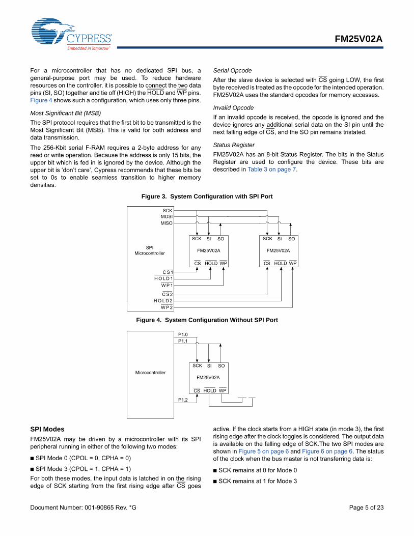
For a microcontroller that has no dedicated SPI bus, ageneral-purpose port may be used. To reduce hardwareresources on the controller, it is possible to connect the two datapins (SI, SO) together and tie off (HIGH) the HOLD and WP pins.Figure 4 shows such a configuration, which uses only three pins.
Most Significant Bit (MSB)
The SPI protocol requires that the first bit to be transmitted is theMost Significant Bit (MSB). This is valid for both address anddata transmission.
The 256-Kbit serial F-RAM requires a 2-byte address for anyread or write operation. Because the address is only 15 bits, theupper bit which is fed in is ignored by the device. Although theupper bit is ‘don’t care’, Cypress recommends that these bits beset to 0s to enable seamless transition to higher memorydensities.
Serial Opcode
After the slave device is selected with CS going LOW, the firstbyte received is treated as the opcode for the intended operation.FM25V02A uses the standard opcodes for memory accesses.
Invalid Opcode
If an invalid opcode is received, the opcode is ignored and thedevice ignores any additional serial data on the SI pin until thenext falling edge of CS, and the SO pin remains tristated.
Status Register
FM25V02A has an 8-bit Status Register. The bits in the StatusRegister are used to configure the device. These bits aredescribed in Table 3 on page 7.
SPI Modes
FM25V02A may be driven by a microcontroller with its SPIperipheral running in either of the following two modes:
■ SPI Mode 0 (CPOL = 0, CPHA = 0)
■ SPI Mode 3 (CPOL = 1, CPHA = 1)
For both these modes, the input data is latched in on the risingedge of SCK starting from the first rising edge after CS goes
active. If the clock starts from a HIGH state (in mode 3), the firstrising edge after the clock toggles is considered. The output datais available on the falling edge of SCK.The two SPI modes areshown in Figure 5 on page 6 and Figure 6 on page 6. The statusof the clock when the bus master is not transferring data is:
■ SCK remains at 0 for Mode 0
■ SCK remains at 1 for Mode 3
Figure 3. System Configuration with SPI Port
Figure 4. System Configuration Without SPI Port
C S 1
C S 2
H O L D 1
H O L D 2
FM25V02A FM25V02A
W P 1
W P 2
SCK SI SO SCK SI SO
CS HOLD WP CS HOLD WP
SCKMOSIMISO
SPIMicrocontroller
FM25V02AMicrocontroller
SCK SI SO
CS HOLD WP
P1.2
P1.1P1.0

FM25V02A
Document Number: 001-90865 Rev. *G Page 6 of 23
The device detects the SPI mode from the status of the SCK pinwhen the device is selected by bringing the CS pin LOW. If theSCK pin is LOW when the device is selected, SPI Mode 0 isassumed and if the SCK pin is HIGH, it works in SPI Mode 3.
Power-Up to First Access
The FM25V02A is not accessible for a tPU time after power-up.Users must comply with the timing parameter tPU, which is theminimum time from VDD (min) to the first CS LOW.
Command Structure
There are nine commands, called opcodes, that can be issuedby the bus master to the FM25V02A. They are listed in Table 1.These opcodes control the functions performed by the memory.
WREN - Set Write Enable Latch
The FM25V02A will power up with writes disabled. The WRENcommand must be issued before any write operation. Sendingthe WREN opcode allows the user to issue subsequent opcodesfor write operations. These include writing the Status Register(WRSR) and writing the memory (WRITE).
Sending the WREN opcode causes the internal Write EnableLatch to be set. A flag bit in the Status Register, called WEL,indicates the state of the latch. WEL = ‘1’ indicates that writes arepermitted. Attempting to write the WEL bit in the Status Registerhas no effect on the state of this bit - only the WREN opcode canset this bit. The WEL bit will be automatically cleared on the risingedge of CS following a WRDI, a WRSR, or a WRITE operation.This prevents further writes to the Status Register or the F-RAMarray without another WREN command. Figure 7 illustrates theWREN command bus configuration.
WRDI - Reset Write Enable Latch
The WRDI command disables all write activity by clearing theWrite Enable Latch. The user can verify that writes are disabledby reading the WEL bit in the Status Register and verifying thatWEL is equal to ‘0’. Figure 8 illustrates the WRDI command busconfiguration.
Figure 5. SPI Mode 0
Figure 6. SPI Mode 3
Table 1. Opcode Commands
Name Description Opcode
WREN Set write enable latch 0000 0110b
WRDI Reset write enable latch 0000 0100b
RDSR Read Status Register 0000 0101b
WRSR Write Status Register 0000 0001b
READ Read memory data 0000 0011b
FSTRD Fast read memory data 0000 1011b
WRITE Write memory data 0000 0010b
SLEEP Enter sleep mode 1011 1001b
RDID Read device ID 1001 1111b
Reserved Reserved 1100 0011b
1100 0010b
0101 1010b
0101 1011b
LSBMSB
7 6 5 4 3 2 1 0
CS
SCK
SI
0 1 2 3 4 5 6 7
CS
SCK
SI 7 6 5 4 3 2 1 0
LSBMSB
0 1 2 3 4 5 6 7
Figure 7. WREN Bus Configuration
Figure 8. WRDI Bus Configuration
0 0 0 0 0 1 1 0
CS
SCK
SI
SOHI-Z
0 1 2 3 4 5 6 7
0 0 0
CS
SCK
SI
SOHI-Z
0 1 2 3 4 5 6 7
0 00 0 1

FM25V02A
Document Number: 001-90865 Rev. *G Page 7 of 23
Status Register and Write ProtectionThe write protection features of the FM25V02A are multi-tiered and are enabled through the status register. The status register isorganized as follows (the default value shipped from the factory for bits in the status register is ‘0’):
Bits 0 and 4-6 are fixed at ‘0’; none of these bits can be modified.Note that bit 0 ("Ready or Write in progress” bit in serial flash andEEPROM) is unnecessary, as the F-RAM writes in real-time andis never busy, so it reads out as a ‘0’. An exception to this is whenthe device is waking up from sleep mode, which is described inSleep Mode on page 10. The BP1 and BP0 control the softwarewrite-protection features and are nonvolatile bits. The WEL flagindicates the state of the Write Enable Latch. Attempting todirectly write the WEL bit in the Status Register has no effect onits state. This bit is internally set and cleared via the WREN andWRDI commands, respectively.
BP1 and BP0 are memory block write protection bits. Theyspecify portions of memory that are write-protected as shown inTable 4.
The BP1 and BP0 bits and the Write Enable Latch are the onlymechanisms that protect the memory from writes. The remainingwrite protection features protect inadvertent changes to the blockprotect bits.
The write protect enable bit (WPEN) in the Status Registercontrols the effect of the hardware write protect (WP) pin. Whenthe WPEN bit is set to '0', the status of the WP pin is ignored.When the WPEN bit is set to '1', a LOW on the WP pin inhibits a
write to the Status Register. Thus the Status Register iswrite-protected only when WPEN = '1' and WP = '0'.
Table 5 summarizes the write protection conditions.
RDSR - Read Status Register
The RDSR command allows the bus master to verify thecontents of the Status Register. Reading the status registerprovides information about the current state of thewrite-protection features. Following the RDSR opcode, theFM25V02A will return one byte with the contents of the StatusRegister.
WRSR - Write Status Register
The WRSR command allows the SPI bus master to write into theStatus Register and change the write protect configuration bysetting the WPEN, BP0, and BP1 bits as required. Prior toissuing a WRSR command, the WP pin must be HIGH orinactive. Note that on the FM25V02A, WP only prevents writingto the Status Register, not the memory array. Before sending theWRSR command, the user must send a WREN command toenable writes. Executing a WRSR command is a write operationand therefore, clears the Write Enable Latch.
Table 2. Status Register
Bit 7 Bit 6 Bit 5 Bit 4 Bit 3 Bit 2 Bit 1 Bit 0
WPEN (0) X (0) X (0) X (0) BP1 (0) BP0 (0) WEL (0) X (0)
Table 3. Status Register Bit Definition
Bit Definition Description
Bit 0 Don’t care This bit is non-writable and always returns ‘0’ upon read.
Bit 1 (WEL) Write Enable WEL indicates if the device is write enabled. This bit defaults to ‘0’ (disabled) on power-up.WEL = '1' --> Write enabled WEL = '0' --> Write disabled
Bit 2 (BP0) Block Protect bit ‘0’ Used for block protection. For details, see Table 4 on page 7.
Bit 3 (BP1) Block Protect bit ‘1’ Used for block protection. For details, see Table 4 on page 7.
Bit 4-6 Don’t care These bits are non-writable and always return ‘0’ upon read.
Bit 7 (WPEN) Write Protect Enable bit Used to enable the function of Write Protect Pin (WP). For details, see Table 5 on page 7.
Table 4. Block Memory Write Protection
BP1 BP0 Protected Address Range
0 0 None
0 1 6000h to 7FFFh (upper 1/4)
1 0 4000h to 7FFFh (upper 1/2)
1 1 0000h to 7FFFh (all)
Table 5. Write Protection
WEL WPEN WP Protected Blocks
Unprotected Blocks
Status Register
0 X X Protected Protected Protected
1 0 X Protected Unprotected Unprotected
1 1 0 Protected Unprotected Protected
1 1 1 Protected Unprotected Unprotected

FM25V02A
Document Number: 001-90865 Rev. *G Page 8 of 23
Memory Operation
The SPI interface, which is capable of a high clock frequency,highlights the fast write capability of the F-RAM technology.Unlike serial flash and EEPROMs, the FM25V02A can performsequential writes at bus speed. No page register is needed andany number of sequential writes may be performed.
Write Operation
All writes to the memory begin with a WREN opcode with CSbeing asserted and deasserted. The next opcode is WRITE. TheWRITE opcode is followed by a two-byte address containing the15-bit address (A14-A0) of the first data byte to be written intothe memory. The upper bit of the two-byte address is ignored.Subsequent bytes are data bytes, which are written sequentially.Addresses are incremented internally as long as the bus mastercontinues to issue clocks and keeps CS LOW. If the last addressof 7FFFh is reached, the counter will roll over to 0000h. Data iswritten MSB first. The rising edge of CS terminates a writeoperation. A write operation is shown in Figure 11.
Note When a burst write reaches a protected block address, theautomatic address increment stops and all the subsequent databytes received for write will be ignored by the device.
EEPROMs use page buffers to increase their write throughput.This compensates for the technology's inherently slow writeoperations. F-RAM memories do not have page buffers becauseeach byte is written to the F-RAM array immediately after it is
clocked in (after the eighth clock). This allows any number ofbytes to be written without page buffer delays.
Note If the power is lost in the middle of the write operation, onlythe last completed byte will be written.
Read Operation
After the falling edge of CS, the bus master can issue a READopcode. Following the READ command is a two-byte addresscontaining the 15-bit address (A14-A0) of the first byte of theread operation. The upper bit of the address is ignored. After theopcode and address are issued, the device drives out the readdata on the next eight clocks. The SI input is ignored during readdata bytes. Subsequent bytes are data bytes, which are read outsequentially. Addresses are incremented internally as long asthe bus master continues to issue clocks and CS is LOW. If thelast address of 7FFFh is reached, the counter will roll over to0000h. Data is read MSB first. The rising edge of CS terminatesa read operation and tristates the SO pin. A read operation isshown in Figure 12.
Fast Read Operation
The FM25V02A supports a FAST READ opcode (0Bh) that isprovided for code compatibility with serial flash devices. TheFAST READ opcode is followed by a two-byte addresscontaining the 15-bit address (A14-A0) of the first byte of theread operation and then a dummy byte. The dummy byte insertsa read latency of an 8-clock cycle. The fast read operation isotherwise the same as an ordinary read operation except that it
Figure 9. RDSR Bus Configuration
Figure 10. WRSR Bus Configuration (WREN not shown)
CS
SCK
SO
0 1 2 3 4 5 6 7
SI 0 0 0 0 0 1 0 01
HI-Z
0 1 2 3 4 5 6 7
LSBD0D1D2D3D4D5D6
MSBD7
Opcode
Data
CS
SCK
SO
0 1 2 3 4 5 6 7
SI 0 0 0 0 0 0 0 1MSB LSB
D2D3D7
HI-Z
0 1 2 3 4 5 6 7
Opcode Data
XX XXX

FM25V02A
Document Number: 001-90865 Rev. *G Page 9 of 23
requires an additional dummy byte. After receiving the opcode,address, and a dummy byte, the FM25V02A starts driving its SOline with data bytes, with the MSB first, and continues trans-mitting as long as the device is selected and the clock isavailable. In case of bulk read, the internal address counter isincremented automatically, and after the last address 7FFFh is
reached, the counter rolls over to 0000h. When the device isdriving data on its SO line, any transition on its SI line is ignored.The rising edge of CS terminates a fast read operation andtristates the SO pin. A Fast Read operation is shown in Figure 13.
Figure 11. Memory Write (WREN not shown) Operation
Figure 12. Memory Read Operation
Figure 13. Fast Read Operation
~ ~
CS
SCK
SO
0 1 2 3 4 5 6 7 0 7654321 12 13 14 15 0 1 2 3 4 5 6 7
MSB LSB
Data
D0D1D2D3D4D5D6D7SI
~ ~
Opcode
0 0 0 0 0 0 1 X A14 A13 A12 A11 A90 A10 A8 A3 A1A2 A0
15-bit Address
MSB LSBHI-Z
~ ~CS
SCK
SO
0 1 2 3 4 5 6 7 0 7654321 12 13 14 15 0 1 2 3 4 5 6 7
MSB LSB
Data
SI
~ ~
Opcode
0 0 0 0 0 0 1 X A14 A13 A12 A11 A91 A10 A8 A3 A1A2 A0
15-bit Address
MSB LSB
D0D1D2D3D4D5D6D7 HI-Z
~ ~
CS
SCK
SO
0 1 2 3 4 5 6 7 0 7654321 12 13 14 15 16 17 18 19 20 21 22 23
Data
SI
~ ~
Opcode
0 0 0 0 1 0 1 X A14 A13 A11 A91 A10 A8 A3 A1A2 A0
15-bit Address
MSB LSB
MSB LSBD0D1D2D3D4D5D6D7
0 1 2 3 4 5 6 7
XXXXXXXX
Dummy Byte
HI-Z
A12

FM25V02A
Document Number: 001-90865 Rev. *G Page 10 of 23
HOLD Pin Operation
The HOLD pin can be used to interrupt a serial operation withoutaborting it. If the bus master pulls the HOLD pin LOW while SCKis LOW, the current operation will pause. Taking the HOLD pin
HIGH while SCK is LOW will resume an operation. Thetransitions of HOLD must occur while SCK is LOW, but the SCKand CS pin can toggle during a hold state.
Sleep Mode
A low-power sleep mode is implemented on the FM25V02Adevice. The device will enter the low-power state when theSLEEP opcode B9h is clocked-in and a rising edge of CS isapplied. When in sleep mode, the SCK and SI pins are ignoredand SO will be HI-Z, but the device continues to monitor the CS
pin. On the next falling edge of CS, the device will return tonormal operation within tREC time. The SO pin remains in a HI-Zstate during the wakeup period. The device does not necessarilyrespond to an opcode within the wakeup period. To start thewakeup procedure, the controller may send a “dummy” read, forexample, and wait the remaining tREC time.
Figure 14. HOLD Operation [2]
CS
SCK
HOLD
SO
~ ~~ ~
SI VALID IN VALID IN~ ~
~ ~
~ ~
Figure 15. Sleep Mode Operation
CS
SCK
SI
SOHI-Z
0
Enters Sleep Mode
VALID IN
tSU
tREC Recovers from Sleep Mode
1 0 1 1 1 0 0 1
1 2 3 4 5 6 7
Note2. Figure 14 shows the HOLD operation for input mode and output mode.
FM25V02A
Document Number: 001-90865 Rev. *G Page 11 of 23
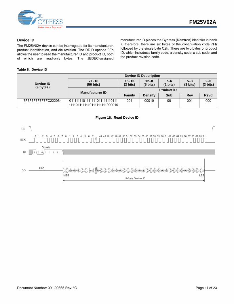
Device ID
The FM25V02A device can be interrogated for its manufacturer,product identification, and die revision. The RDID opcode 9Fhallows the user to read the manufacturer ID and product ID, bothof which are read-only bytes. The JEDEC-assigned
manufacturer ID places the Cypress (Ramtron) identifier in bank7; therefore, there are six bytes of the continuation code 7Fhfollowed by the single byte C2h. There are two bytes of productID, which includes a family code, a density code, a sub code, andthe product revision code.
Table 6. Device ID
Device ID(9 bytes)
Device ID Description
71–16(56 bits)
15–13 (3 bits)
12–8 (5 bits)
7–6(2 bits)
5–3 (3 bits)
2–0 (3 bits)
Manufacturer IDProduct ID
Family Density Sub Rev Rsvd
7F7F7F7F7F7FC22208h 01111111011111110111111101111111011111110111111111000010
001 00010 00 001 000
Figure 16. Read Device ID
CS
SCK
SO
SI
Opcode
~ ~
0 1 2 3 4 5 6 7 0 7654321 44 45 46 55 56 57 58 59 60 61 62 63 64 65 66 67 68 69 70 71
1 0 0 1 1 1 1 1
LSBMSB
HI-Z
~ ~
47 48 49 50 51 52 53 54
9-Byte Device ID
D7 D6 D5 D4 D3 D2 D1 D0 D3 D1 D7D2 D0 D5 D3 D1D4 D2 D7 D5 D3D6 D4D6 D0 D1 D7 D5D0 D6 D3 D1D2 D0D2 D4

FM25V02A
Document Number: 001-90865 Rev. *G Page 12 of 23
Endurance
The FM25V02A devices are capable of being accessed at least1014 times, reads or writes. An F-RAM memory operates with aread and restore mechanism. Therefore, an endurance cycle isapplied on a row basis for each access (read or write) to thememory array. The F-RAM architecture is based on an array ofrows and columns of 4K rows of 64-bits each. The entire row isinternally accessed once whether a single byte or all eight bytesare read or written. Each byte in the row is counted only once inan endurance calculation. Table 7 shows endurance calculationsfor a 64-byte repeating loop, which includes an opcode, a startingaddress, and a sequential 64-byte data stream. This causeseach byte to experience one endurance cycle through the loop.
Table 7. Time to Reach Endurance Limit for Repeating 64-byte Loop
SCK Freq (MHz)
Endurance Cycles/sec
Endurance Cycles/year
Years to Reach Limit
40 74,620 2.35 × 10¹² 42.6
20 37,310 1.18 × 10¹² 85.1
10 18,660 5.88 × 10¹¹ 170.2
5 9,330 2.94 × 10¹¹ 340.3

FM25V02A
Document Number: 001-90865 Rev. *G Page 13 of 23
Maximum Ratings
Exceeding maximum ratings may shorten the useful life of thedevice. These user guidelines are not tested.
Storage temperature ............................... –55 C to + 125 C
Maximum accumulated storage time At 125 °C ambient temperature ................................. 1000 hAt 85 °C ambient temperature ................................ 10 Years
Ambient temperature with power applied ................................... –55 °C to +125 °C
Supply voltage on VDD relative to VSS ........–1.0 V to + 4.5 V
Input voltage ........... –1.0 V to +4.5 V and VIN < VDD + 1.0 V
DC voltage applied to outputs in HI-Z state ........................................ –0.5 V to VDD + 0.5 V
Transient voltage (< 20 ns) on any pin to ground potential ................. –2.0 V to VDD + 2.0 V
Package power dissipation capability (TA = 25 °C) ................................................. 1.0 W
Surface mount lead soldering temperature (3 seconds) ........................................ + 260 C
DC output current (1 output at a time, 1s duration) .... 15 mA
Electrostatic discharge voltage Human Body Model (JEDEC Std JESD22-A114-B) ................ 2 kV
Charged Device Model (JEDEC Std JESD22-C101-A)........... 500 V
Latch-up current .................................................... > 140 mA
Operating Range
Range Ambient Temperature (TA) VDD
Industrial –40 C to +85 C 2.0 V to 3.6 V
DC Electrical Characteristics
Over the Operating Range
Parameter Description Test Conditions Min Typ[3] Max Unit
VDD Power supply 2.0 3.3 3.6 V
IDD VDD supply current SCK toggling between VDD –0.2 V and VSS, other inputs VSSor VDD – 0.2 V. SO = Open.
fSCK = 40 MHz – – 2.5 mA
fSCK = 1 MHz – – 0.22 mA
ISB VDD standby current CS = VDD. All other inputs VSS or VDD. – 90 150 A
IZZ Sleep mode current CS = VDD. All other inputs VSS or VDD. – 5 8 A
ILI Input leakage current (Except HOLD)
VSS < VIN < VDD –1 – +1 A
Input leakage current (for HOLD)
–100 – +1 A
ILO Output leakage current VSS < VOUT < VDD –1 – +1 A
VIH Input HIGH voltage 0.7 × VDD – VDD + 0.3 V
VIL Input LOW voltage – 0.3 – 0.3 × VDD V
VOH1 Output HIGH voltage IOH = –1 mA, VDD = 2.7 V. 2.4 – – V
VOH2 Output HIGH voltage IOH = –100 A VDD – 0.2 – – V
VOL1 Output LOW voltage IOL = 2 mA, VDD = 2.7 V – – 0.4 V
VOL2 Output LOW voltage IOL = 150 A – – 0.2 V
Rin[4] Input resistance (HOLD) For VIN = VIL (max) 800 – – k
For VIN = VIH (min) 30 – – k
Notes3. Typical values are at 25 °C, VDD = VDD (typ). Not 100% tested.4. The input pull-up circuit is strong (30 k) when the input voltage is above VIH and weak (800 k) when the input voltage is below VIL.

FM25V02A
Document Number: 001-90865 Rev. *G Page 14 of 23
AC Test Conditions
Input pulse levels .................................10% and 90% of VDD
Input rise and fall times ...................................................3 ns
Input and output timing reference levels ................0.5 × VDD
Output load capacitance .............................................. 30 pF
Data Retention and Endurance
Parameter Description Test condition Min Max Unit
TDR Data retention TA = 85 C 10 – Years
TA = 75 C 38 –
TA = 65 C 151 –
NVC Endurance Over operating temperature 1014 – Cycles
Capacitance
Parameter [5] Description Test Conditions Max Unit
CO Output pin capacitance (SO) TA = 25 C, f = 1 MHz, VDD = VDD (typ) 8 pF
CI Input pin capacitance 6 pF
Thermal Resistance
Parameter Description Test Conditions 8-pin SOIC 8-pin DFN Unit
JA Thermal resistance (junction to ambient)
Test conditions follow standard test methodsand procedures for measuring thermalimpedance, per EIA/ JESD51.
146 31 C/W
JC Thermal resistance (junction to case)
48 35 C/W
Note5. This parameter is periodically sampled and not 100% tested.

FM25V02A
Document Number: 001-90865 Rev. *G Page 15 of 23
AC Switching Characteristics
Over the Operating Range
Parameters [6]
DescriptionVDD = 2.0 V to 3.6 V VDD = 2.7 V to 3.6 V
UnitCypress Parameter
Alt. Parameter Min Max Min Max
fSCK – SCK clock frequency 0 25 0 40 MHz
tCH – Clock HIGH time 18 – 11 – ns
tCL – Clock LOW time 18 – 11 – ns
tCSU tCSS Chip select setup 12 – 10 – ns
tCSH tCSH Chip select hold 12 – 10 – ns
tOD[7, 8] tHZCS Output disable time – 20 – 12 ns
tODV tCO Output data valid time – 16 – 9 ns
tOH – Output hold time 0 – 0 – ns
tD – Deselect time 60 – 40 – ns
tR[9, 10] – Data in rise time – 50 – 50 ns
tF[9, 10] – Data in fall time – 50 – 50 ns
tSU tSD Data setup time 8 – 5 – ns
tH tHD Data hold time 8 – 5 – ns
tHS tSH HOLD setup time 12 – 10 – ns
tHH tHH HOLD hold time 12 – 10 – ns
tHZ[7, 8] tHHZ HOLD LOW to HI-Z – 25 – 20 ns
tLZ[8] tHLZ HOLD HIGH to data active – 25 – 20 ns
Notes6. Test conditions assume a signal transition time of 3 ns or less, timing reference levels of 0.5 × VDD, input pulse levels of 10% to 90% of VDD, output loading of the
specified IOL/IOH and 30 pF load capacitance shown in AC Test Conditions.7. tOD and tHZ are specified with a load capacitance of 5 pF. Transition is measured when the outputs enter a high impedance state.8. Characterized but not 100% tested in production.9. Rise and fall times measured between 10% and 90% of waveform.10. These parameters are guaranteed by design and are not tested.

FM25V02A
Document Number: 001-90865 Rev. *G Page 16 of 23
Figure 17. Synchronous Data Timing (Mode 0)
Figure 18. HOLD Timing
HI-Z
VALID IN
HI-Z
CS
SCK
SI
SO
tCLtCHtCSU
tSU tH
tODV tOH
tD
tCSH
tOD
VALID IN VALID IN
CS
SCK
HOLD
SO
tHS
tHZ tLZ
tHHtHS
tHH
~ ~~ ~
SI
tSU
VALID IN VALID IN
~ ~
~ ~
~ ~

FM25V02A
Document Number: 001-90865 Rev. *G Page 17 of 23
Power Cycle Timing
Over the Operating Range
Parameter Description Min Max Unit
tPU Power-up VDD (min) to first access (CS LOW) 250 – μs
tPDLast access (CS HIGH) to power-down (VDD(min)) 0 – µs
tVR [11, 12] VDD power-up ramp rate 50 – µs/V
tVF [11, 12] VDD power-down ramp rate 100 – µs/V
tREC [13] Recovery time from sleep mode – 400 µs
Figure 19. Power Cycle Timing
CS
~ ~~ ~
tPU
tVR tVFVDD
VDD(min)
tPD
VDD(min)
Notes11. Slope measured at any point on VDD waveform.12. These parameters are guaranteed by design and are not tested.13. Refer to Figure 15 on page 10 for sleep mode recovery timing.

FM25V02A
Document Number: 001-90865 Rev. *G Page 18 of 23
Ordering Code Definitions
Ordering Information
Ordering Code Package Diagram Package Type Operating Range
FM25V02A-G 51-85066 8-pin SOIC Industrial
FM25V02A-GTR 51-85066 8-pin SOIC
FM25V02A-DG 001-85260 8-pin DFN
FM25V02A-DGTR 001-85260 8-pin DFN
All these parts are Pb-free. Contact your local Cypress sales representative for availability of these parts.
Option: Blank = Standard; TR = Tape and Reel
Package Type: X = G or DG G = 8-pin SOIC; DG = 8-pin DFN
Device revision: A
Density: 02 = 256-Kbit
Voltage: V = 2.0 V to 3.6 V
SPI F-RAM
Cypress
25FM V 02 - X TRA

FM25V02A
Document Number: 001-90865 Rev. *G Page 19 of 23
Package DiagramsFigure 20. 8-pin SOIC (150 Mils) Package Outline, 51-85066
51-85066 *H

FM25V02A
Document Number: 001-90865 Rev. *G Page 20 of 23
Figure 21. 8-pin DFN (4.0 mm × 4.5 mm × 0.8 mm) Package Outline, 001-85260
Package Diagrams (continued)
001-85260 *B
FM25V02A
Document Number: 001-90865 Rev. *G Page 21 of 23
Acronyms Document Conventions
Units of MeasureAcronym Description
CPHA Clock Phase
CPOL Clock Polarity
DFN Dual Flat No-lead
EEPROM Electrically Erasable Programmable Read-OnlyMemory
EIA Electronic Industries Alliance
F-RAM Ferroelectric Random Access Memory
I/O Input/Output
JEDEC Joint Electron Devices Engineering Council
JESD JEDEC Standards
LSB Least Significant Bit
MSB Most Significant Bit
RoHS Restriction of Hazardous Substances
SPI Serial Peripheral Interface
SOIC Small Outline Integrated Circuit
Symbol Unit of Measure
°C degree Celsius
Hz hertz
kHz kilohertz
k kilohm
Kbit Kilobit
MHz megahertz
A microampere
F microfarad
s microsecond
mA milliampere
ms millisecond
ns nanosecond
ohm
% percent
pF picofarad
V volt
W watt

FM25V02A
Document Number: 001-90865 Rev. *G Page 22 of 23
Document History Page
Document Title: FM25V02A, 256-Kbit (32K × 8) Serial (SPI) F-RAMDocument Number: 001-90865
Rev. ECN No. Orig. of Change
Submission Date Description of Change
** 4265427 GVCH 01/29/2014 New data sheet.
*A 4390913 GVCH 06/20/2014 Changed status from Advance to Preliminary.Updated Pin Definitions: Updated details in “Description” column of “HOLD” pin (Added the sentence,“This pin has a weak internal pull-up (refer to the RIN spec in DC ElectricalCharacteristics)”).Updated Maximum Ratings:Removed “Machine Model” under “Electrostatic Discharge Voltage”.Updated DC Electrical Characteristics: Added typical value for ISB and IZZ parameters.Changed minimum value of Rin parameter from 40 kto 30 kcorrespondingto Test Condition “VIN = VIH(min)”.Changed minimum value of Rin parameter from 1 Mto 800 kcorrespondingto Test Condition “VIN = VIL(max)”.Updated Note 4. Updated Thermal Resistance: Added thermal resistance values.
*B 4571858 GVCH 11/18/2014 Updated Serial Peripheral Interface - SPI Bus:Updated Command Structure:Updated Table 1: Added reserved opcodes - 0xC3, 0xC2, 0x5A, 0x5B.
*C 4197512 ZSK 02/10/2015 Changed status from Preliminary to Final.Replaced “TDFN” with “DFN” in all instances across the document.Updated Functional Description:Added “For a complete list of related resources, click here.” at the end.Updated Pin Definitions:Updated details in “Description” column of “EXPOSED PAD” pin.Updated Package Diagrams:spec 51-85066 – Changed revision from *F to *G.
*D 4784430 GVCH 06/02/2015 Updated Package Diagrams:spec 001-85260 – Changed revision from *A to *B.Updated to new template.
*E 4879715 ZSK / PSR 08/11/2015 Updated Maximum Ratings:Removed “Maximum junction temperature”.Added “Maximum accumulated storage time”.Added “Ambient temperature with power applied”.
*F 5085935 GVCH 01/14/2016 Updated Ordering Information: Updated part numbers.Updated Package Diagrams:spec 51-85066 – Changed revision from *G to *H.
*G 5450688 ZSK 09/27/2016 Updated Power Cycle Timing: Changed minimum value of tPU parameter from 1 ms to 250 μs.Updated to new template.

Document Number: 001-90865 Rev. *G Revised September 27, 2016 Page 23 of 23
FM25V02A
© Cypress Semiconductor Corporation, 2014-2016. This document is the property of Cypress Semiconductor Corporation and its subsidiaries, including Spansion LLC ("Cypress"). This document,including any software or firmware included or referenced in this document ("Software"), is owned by Cypress under the intellectual property laws and treaties of the United States and other countriesworldwide. Cypress reserves all rights under such laws and treaties and does not, except as specifically stated in this paragraph, grant any license under its patents, copyrights, trademarks, or otherintellectual property rights. If the Software is not accompanied by a license agreement and you do not otherwise have a written agreement with Cypress governing the use of the Software, then Cypresshereby grants you a personal, non-exclusive, nontransferable license (without the right to sublicense) (1) under its copyright rights in the Software (a) for Software provided in source code form, tomodify and reproduce the Software solely for use with Cypress hardware products, only internally within your organization, and (b) to distribute the Software in binary code form externally to end users(either directly or indirectly through resellers and distributors), solely for use on Cypress hardware product units, and (2) under those claims of Cypress's patents that are infringed by the Software (asprovided by Cypress, unmodified) to make, use, distribute, and import the Software solely for use with Cypress hardware products. Any other use, reproduction, modification, translation, or compilationof the Software is prohibited.
TO THE EXTENT PERMITTED BY APPLICABLE LAW, CYPRESS MAKES NO WARRANTY OF ANY KIND, EXPRESS OR IMPLIED, WITH REGARD TO THIS DOCUMENT OR ANY SOFTWAREOR ACCOMPANYING HARDWARE, INCLUDING, BUT NOT LIMITED TO, THE IMPLIED WARRANTIES OF MERCHANTABILITY AND FITNESS FOR A PARTICULAR PURPOSE. To the extentpermitted by applicable law, Cypress reserves the right to make changes to this document without further notice. Cypress does not assume any liability arising out of the application or use of anyproduct or circuit described in this document. Any information provided in this document, including any sample design information or programming code, is provided only for reference purposes. It isthe responsibility of the user of this document to properly design, program, and test the functionality and safety of any application made of this information and any resulting product. Cypress productsare not designed, intended, or authorized for use as critical components in systems designed or intended for the operation of weapons, weapons systems, nuclear installations, life-support devices orsystems, other medical devices or systems (including resuscitation equipment and surgical implants), pollution control or hazardous substances management, or other uses where the failure of thedevice or system could cause personal injury, death, or property damage ("Unintended Uses"). A critical component is any component of a device or system whose failure to perform can be reasonablyexpected to cause the failure of the device or system, or to affect its safety or effectiveness. Cypress is not liable, in whole or in part, and you shall and hereby do release Cypress from any claim,damage, or other liability arising from or related to all Unintended Uses of Cypress products. You shall indemnify and hold Cypress harmless from and against all claims, costs, damages, and otherliabilities, including claims for personal injury or death, arising from or related to any Unintended Uses of Cypress products.
Cypress, the Cypress logo, Spansion, the Spansion logo, and combinations thereof, WICED, PSoC, CapSense, EZ-USB, F-RAM, and Traveo are trademarks or registered trademarks of Cypress inthe United States and other countries. For a more complete list of Cypress trademarks, visit cypress.com. Other names and brands may be claimed as property of their respective owners.
Sales, Solutions, and Legal Information
Worldwide Sales and Design Support
Cypress maintains a worldwide network of offices, solution centers, manufacturer’s representatives, and distributors. To find the office closest to you, visit us at Cypress Locations.
Products
ARM® Cortex® Microcontrollers cypress.com/arm
Automotive cypress.com/automotive
Clocks & Buffers cypress.com/clocks
Interface cypress.com/interface
Internet of Things cypress.com/iot
Lighting & Power Control cypress.com/powerpsoc
Memory cypress.com/memory
PSoC cypress.com/psoc
Touch Sensing cypress.com/touch
USB Controllers cypress.com/usb
Wireless/RF cypress.com/wireless
PSoC®Solutions
PSoC 1 | PSoC 3 | PSoC 4 | PSoC 5LP
Cypress Developer Community
Forums | Projects | Video | Blogs | Training | Components
Technical Support
cypress.com/support