Islanding Detection in Power Electronic Converter Based Distributed Generation
Publ ic Interest Energy Research (P IER) Program FINAL PROJECT REPORT
FLEXIBLE DISTRIBUTED ENERGY RESOURCE UTILITY INTERFACE
Prepared for: California Energy Commission Prepared by: National Renewable Energy Laboratory and Northern Power Systems, Inc.
JUNE 2012CEC ‐500 ‐2012 ‐070

Prepared by: Primary Author(s): Ben Kroposki National Renewable Energy Laboratory and Northern Power Systems, Inc. Golden, Colorado 80401 Contract Number: 500-03-011 Prepared for: California Energy Commission Bernard Treanton Project Manager Mike Gravely Office Manager Energy Systems Research Office Laurie ten Hope Deputy Director RESEARCH AND DEVELOPMENT DIVISION Robert P. Oglesby Executive Director
DISCLAIMER This report was prepared as the result of work sponsored by the California Energy Commission. It does not necessarily represent the views of the Energy Commission, its employees or the State of California. The Energy Commission, the State of California, its employees, contractors and subcontractors make no warrant, express or implied, and assume no legal liability for the information in this report; nor does any party represent that the uses of this information will not infringe upon privately owned rights. This report has not been approved or disapproved by the California Energy Commission nor has the California Energy Commission passed upon the accuracy or adequacy of the information in this report.
i
Acknowledgments
Northern Power Systems gratefully acknowledges the National Renewable Energy Laboratory and the California Energy Commission for their support of this research and development effort under National Renewable Energy Laboratory Subcontract ZAT‐4‐32616‐05, which makes this effort possible.
Please cite this report as follows:
Lynch, J., V. John, S. M. Danial, E. Benedict, and I. Vihinen (Northern Power Systems Inc.) and B. Kroposki and C. Pink (National Renewable Energy Laboratory). 2006. Flexible DER Utility Interface System: Final Report September 2004–May 2006. California Energy Commission, PIER Energy Systems Integration Program. CEC‐500‐2012‐070.

ii

iii
Preface
The California Energy Commission’s Public Interest Energy Research (PIER) Program supports public interest energy research and development that will help improve the quality of life in California by bringing environmentally safe, affordable, and reliable energy services and products to the marketplace.
The PIER Program conducts public interest research, development, and demonstration (RD&D) projects to benefit California.
The PIER Program strives to conduct the most promising public interest energy research by partnering with RD&D entities, including individuals, businesses, utilities, and public or private research institutions.
• PIER funding efforts are focused on the following RD&D program areas:
• Buildings End‐Use Energy Efficiency
• Energy Innovations Small Grants
• Energy‐Related Environmental Research
• Energy Systems Integration
• Environmentally Preferred Advanced Generation
• Industrial/Agricultural/Water End‐Use Energy Efficiency
• Renewable Energy Technologies
• Transportation Flexible Distributed Energy Resource Utility Interface System is the final report for the Interconnection, Grid Effects, and Tariff Design for Distributed Energy Resources project (contract number 500‐03‐011) conducted by the National Renewable Energy Laboratory and Northern Power Systems Inc. The information from this project contributes to PIER’s Energy Systems Integration Program.
For more information about the PIER Program, please visit the Energy Commission’s website at www.energy.ca.gov/research or contact the Energy Commission at 916‐654‐5164.

iv

v
Table of Contents
Preface ............................................................................................................................................ iii
Abstract ............................................................................................................................................. xi
Executive Summary ......................................................................................................................... 1
1.0 Introduction ........................................................................................................................ 5
1.1. Universal Grid Interconnect Concept ........................................................................ 5
1.2. DER Switch Program Goals ........................................................................................ 6
2.0 Project Approach................................................................................................................ 7
2.1. DER System Architecture ............................................................................................ 7
2.2. DER Switch Specification and Design ..................................................................... 17
2.3. Component Selection ................................................................................................. 34
3.0 Project Outcomes ............................................................................................................. 49
3.1. Test List and Location ................................................................................................ 49
3.2. Test Setup ..................................................................................................................... 49
3.3. Test Procedure ............................................................................................................. 52
3.4. Test Results .................................................................................................................. 53
3.5. Test Summary ............................................................................................................. 81
4.0 Conclusions and Recommendations ............................................................................. 86
5.0 References ......................................................................................................................... 88
6.0 Glossary ............................................................................................................................. 90
Appendix A: Specification Summary of the DER Switch
Appendix B: Prototype DER Switch Photos
Appendix C: SmartView Documentation
Appendix D: NREL Modeling and Simulation Report
Appendix E: NREL’s Test Report
Appendix F: Omicron Technical Data Sheets
Appendix G: Omicron
vi
List of Figures
Figure 1. Energy Commission PIER DER integration roadmap ................................................... 2
Figure 2. Architecture options for PV installations. ....................................................................... 8
Figure 3. Architecture for wind DG and hybrid wind systems .................................................. 10
Figure 4. DG architecture with dispatchable sources. .................................................................. 12
Figure 5. Interconnection architecture with synchronous machine generators ....................... 14
Figure 6. Power system configurations to feed loads with high power quality requirements .............................................................................................................................. 15
Figure 7. DER switch architecture to connect a Microgrid power network to the grid .......... 17
Figure 8. A typical circuit configuration of a DER Switch ........................................................... 19
Figure 9. DER power network block diagram indicating the target role of the DER Switch .......................................................................................................................................... 20
Figure 10. State diagram for the DER Switch ................................................................................ 24
Figure 11. One‐line schematic of the DER Switch showing sensor locations ........................... 25
Figure 12. The ITIC/CBEMA and SEMIF47 curve......................................................................... 33
Figure 13. SmartView energy management interface .................................................................. 34
Figure 14. Circuit configuration of the DER switch ...................................................................... 35
Figure 15. Topology options for the bidirectional switch ............................................................ 36
Figure 16. Voltage suppression topologies for three phase applications .................................. 37
Figure 17. Clamp capacitor pre‐charge circuit .............................................................................. 42
Figure 18. Clamp discharge circuit ................................................................................................. 43
Figure 19. NPS’s setup for testing the DER Switch in the Waitsfield test facility .................... 51
Figure 20. Voltage and current start‐up transient response of the input and output terminals of the 24 Vdc power supply .................................................................................... 54
Figure 21. Voltage and current steady‐state response of the input and output terminals of the 24Vdc power supply ...................................................................................................... 54
Figure 22. Waveforms that indicate switch connection transition ............................................. 56
Figure 23. Voltage and current waveforms after switch closing ................................................ 56
vii
Figure 24. Waveforms that indicate switch disconnection transition ........................................ 57
Figure 25. Switch response to a large undervoltage event .......................................................... 60
Figure 26. Response of the system to overvoltage event ............................................................. 61
Figure 27. Response of the system to an underfrequency event ................................................. 63
Figure 28. Synchronization tests summary .................................................................................... 74
Figure 29. CBEMA curve specification defined in controller ...................................................... 79
Figure 30. Response to CBEMA (CBEMA voltage #1) .................................................................. 79
Figure 31. Response to CBEMA (CBEMA voltage #5) .................................................................. 80
Figure 32. CBEMA curve test performed at NREL ....................................................................... 81
viii
List of Tables
Table 1. Target voltage and current ranges for DER Switch designs ......................................... 21
Table 2. The relay functions implemented in the DER Switch .................................................... 28
Table 3. Interconnection system response to abnormal voltages ............................................... 30
Table 4. Interconnection system response to abnormal frequencies .......................................... 31
Table 5. Conduction characteristics for two topology options ................................................... 36
Table 6. Estimated operating temperatures ................................................................................... 40
Table 7. Bill of major materials and costs ....................................................................................... 45
Table 8. Summary of the DER Switch program goals and design evaluation .......................... 47
Table 9. Test list, status, and location performed .......................................................................... 50
Table 10. Operation times of DER Switch ...................................................................................... 55
Table 11. Breaker disconnect delay determination (test performed at NREL) ......................... 57
Table 12. Undervoltage relay function test data ........................................................................... 59
Table 13. Overvoltage (59) relay function test data ...................................................................... 61
Table 14. Overfrequency (81O) relay function test data .............................................................. 62
Table 15. Underfrequency (81U) relay function test data ............................................................ 62
Table 16. Overcurrent relay function test data .............................................................................. 64
Table 17. IEEE 1547 specification for interconnection response to overvoltages ..................... 65
Table 18. Switch response to IEEE 1547 overvoltage events ....................................................... 66
Table 19. Voltage trials for trip time test ........................................................................................ 66
Table 20. Overvoltage test results summary (test performed at NREL) .................................... 67
Table 21. IEEE 1547 specification for interconnection response to undervoltages................... 68
Table 22. Switch response to IEEE 1547 undervoltage events .................................................... 69
Table 23. Voltage trials for trip time test ........................................................................................ 69
Table 24. Undervoltage test results summary (test performed at NREL) ................................. 70
Table 25. Interconnection system response to overfrequency ..................................................... 71
Table 26. Trip times for overfrequency trip time test ................................................................... 71

ix
Table 27. Interconnection system response to underfrequency .................................................. 71
Table 28. Trip times for underfrequency trip time test ................................................................ 71
Table 29. Over‐ and underfrequency test results summary (test performed at NREL) .......... 72
Table 30. Synchronization test ......................................................................................................... 73
Table 31. Reverse power magnitude and time constant settings ................................................ 75
Table 32. Anti‐islanding magnitude and time constant settings and test results ..................... 75
Table 33. Anti‐islanding trip time results (test performed at NREL) ........................................ 76
Table 34. Reconnection time and interruption checkout ............................................................. 77
Table 35. Open phase disconnect and reclose test results ........................................................... 77
Table 36. Switch response to interruption voltage according to ITIC‐CBEMA curve ............. 79
Table 37. DER Switch test status and summary ............................................................................ 82

x

xi
Abstract
Interconnection equipment between distributed energy resources and the grid is typically custom‐designed by the distributed generator manufacturer or integrated by engineering firms. The proposed distributed energy resources switch has integrated all the required equipment for the distributed energy resources interconnection into a single package that is designed to be compliant with the standards of Institute of Electrical and Electronics Engineers Inc. 1547 and underrated laboratories 1741. A prototype of a circuit breaker‐based distributed energy resources switch with a digital signal processor board was designed, built, and tested at northern power system and National Renewable Energy Laboratory. The objective was to create a standard, but flexible, universal interface switch for distributed energy resources so that single or multiple distributed energy resource systems can be connected to one utility. The resulting interconnection switch design is distributed energy resource technology‐neutral and can be used for inverter and machine distributed generator applications. Three switch designs were created: circuit breaker, silicon controlled rectifier, and integrated gate bipolar transistor. The circuit breaker design was selected to meet the program’s schedule and budget.
Keywords: distributed generation, distributed energy resources, DG interconnection, islanding, synchronization, protective relaying, IEEE 1547

xii

1
Executive Summary
Introduction In an effort to accelerate deployment of Distributed Energy Resources (DER) such as wind, solar, and conventional backup generators to the nation’s electrical grid, Northern Power Systems, the California Energy Commission, and the National Renewable Energy Laboratory collaborated to create a prototype universal interconnect device called the distributed energy resource Switch.
Our objective is to consolidate the various power and switching functions (for example, power switching, protective relaying, metering, and communications) traditionally provided by relays, hardware, and other components at the utility interface for modern distributed energy resource systems into a single system with a digital signal processor. The distributed energy resource Switch is designed to meet Institute of Electrical and Electronics Engineers Inc. 1547 and UL 1741 grid interconnection standards to minimize custom engineering and site‐specific approval processes and lower cost. To maximize applicability and functionality, it was also designed to be technology neutral (e.g., the controls in the digital signal processor could be used with a circuit breaker, as well as faster semiconductor switching technologies like silicon‐controlled rectifier, integrated gate bipolar transistor, and Integrated Gate Commutated Thyristor technologies) and applicable to distributed energy resource assets with conventional generators or power converters.
This report outlines the applications, design, and testing of the prototype distributed energy resource Switch. Lessons learned from testing this prototype can directly benefit future distributed energy resource Switch prototypes, devices, and products. Figure 1 shows how this distributed generator system interconnection prototype fits in with the Components and Subsystems Platform research and with other areas of the Energy Commission Public Interest Energy Research (PIER) program.
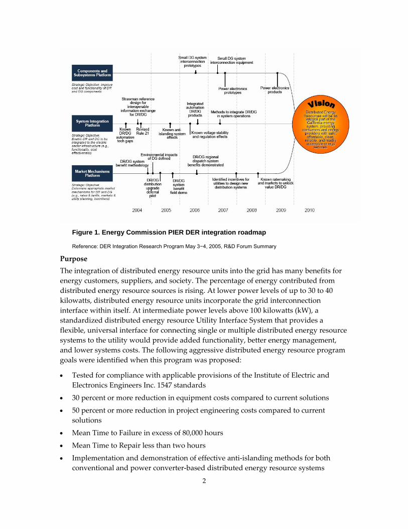
Figure 1. Energy Commission PIER DER integration roadmap
Reference: DER Integration Research Program May 3−4, 2005, R&D Forum Summary
Purpose The integration of distributed energy resource units into the grid has many benefits for energy customers, suppliers, and society. The percentage of energy contributed from distributed energy resource sources is rising. At lower power levels of up to 30 to 40 kilowatts, distributed energy resource units incorporate the grid interconnection interface within itself. At intermediate power levels above 100 kilowatts (kW), a standardized distributed energy resource Utility Interface System that provides a flexible, universal interface for connecting single or multiple distributed energy resource systems to the utility would provide added functionality, better energy management, and lower systems costs. The following aggressive distributed energy resource program goals were identified when this program was proposed:
• Tested for compliance with applicable provisions of the Institute of Electric and Electronics Engineers Inc. 1547 standards
• 30 percent or more reduction in equipment costs compared to current solutions
• 50 percent or more reduction in project engineering costs compared to current solutions
• Mean Time to Failure in excess of 80,000 hours
• Mean Time to Repair less than two hours
• Implementation and demonstration of effective anti‐islanding methods for both conventional and power converter‐based distributed energy resource systems
2

3
• Implementation and demonstration of effective resynchronization methods for both conventional and power converter‐based distributed energy resource systems
• Fully functional and demonstrated energy management interface.
Project Objectives The primary objective of this research was to design, build, and test a working distributed energy resource Switch prototype that meets as many of these goals as possible, given limited time and funding, as well as limited data on traditional solutions and the maturity of the traditional low‐cost products that are on the market today. The specific objectives of the prototype were to: 1) integrate all of the controls and protection functions into a single system and digital signal processor; 2) pass the relevant relay function, Institute of Electrical and Electronic Engineers 1547, power quality, and other tests at Northern Power Systems and National Renewable Energy Laboratory; 3) minimize cost; 4) maximize reliability; and 5) ensure the prototype is compliant with an energy management interface.
Key measures of success of this project are: 1) the creation of a prototype distributed energy resource Switch that integrates all of the controls and protection functions that are typically done by relays and other hardware; 2) the degree to which it meets its relay, Institute of Electrical and Electronics Engineers Inc. 1547, and power quality and other performance goals; and 3) the prototype distributed energy resource Switch’s cost. The technology‐neutral design goal is also an important measure of success that provides the same controls and protection safeguards into the distributed energy resource Switch, but also allows for future tradeoffs between cost, switching speed, and fault protection.
Project Outcomes The distributed energy resource Switch not only represents the creation of a working, low‐cost ($10,000) prototype that validates the concept of integrating all controls and protection functions typically done by relays and other hardware into a single system and digital signal processor for low‐cost circuit breaker‐based technologies, but for all switching technologies, including semiconductor‐based technologies such as integrated gate bipolar transistor, silicon controlled rectifier, and Integrated Gate Commutated Thyristor switches. By designing for the most challenging semiconductor switch technology (Integrated Gate Commutated Thyristor, silicon controlled rectifier), researchers were able to design the system and software to be compatible with slower but significantly cheaper circuit breakers. As a result, they were able to test the distributed energy resource Switch’s critical controls and protection functions with a low‐cost circuit breaker‐based switch.
Highlights of the test results from initial tests carried out at Northern Power Systems and at National Renewable Energy Laboratory’s Distributed Energy Resource Test Facility near Boulder, Colorado, show promising results, substantially meeting the relevant Institute of Electrical and Electronics Engineers Inc. 1547 standard, relay

4
function, and power quality test requirements. With some additional calibrations, minor software numerical precision improvement, and funding, the distributed energy resource Switch could be certified. The results were as follows:
• Relay Function Tests: detected, tripped for over‐ and undervoltage, over‐ and underfrequency, phase sequence, reverse power, instantaneous and time overcurrent, and discrete event trip tests.
• Institute of Electrical and Electronics Engineers Inc. 1547 Tests: detected, tripped for over‐ and undervoltage, over‐ and underfrequency, synchronization, unintentional islanding, reconnection, and open phase tests.
• Power Quality Tests: detected, tripped for three‐phase, but did not meet timing requirements for one‐phase CBEMA/ITIC power quality tests.
Meeting the equipment cost reduction goal was the most challenging. This is especially the case for semiconductor‐based switches, where it can be justified only if grid power quality benefits are evaluated. The circuit breaker‐based distributed energy resource switch had a similar equipment cost compared to current solutions. Further cost reductions at production levels may be possible. The analysis at the design stage indicates that all the remaining project objectives can be met based on the distributed energy resource Switch platform. The prototype’s projected reliability is 29 years for the distributed energy resource design, and the design is compatible with enterprise energy management systems like Northern Power System’s SmartView software.
We expect that the distributed energy resource Switch can be certified to meet grid interconnection requirements with minimal calibration and control timing efforts. The controller has been proven to meet the requirements for both circuit breaker‐ and semiconductor‐based distributed energy resource Switches. Based on the successful tests, the distributed energy resource Switch could be incorporated into a Microgrid power network at the Northern Power Systems facility in Waitsfield, Vermont.
Conclusion and Recommendations A prototype distributed energy resource Switch that integrates all functions provided by relays and other hardware into a single energy management‐compliant system with a digital signal processor was created that substantially meets its Institute of Electrical and Electronics Engineers Inc. 1547, resynchronization, and anti‐islanding goals. Costs were minimized and reliability was maximized. Variations of the distributed energy resource Switch are currently being used now in other Energy Commission projects with distributed energy resource systems. Further studies to enhance its features and lower cost are suggested. The recommendations described in this report include further research to improve the accuracy of its algorithms under balanced and unbalanced conditions and to determine fault current direction at high speed. Further study into the benefits of high‐speed switching will be beneficial in optimizing faster semiconductor‐based distributed energy resource Switches and evaluating production costs.

5
1.0 Introduction
Distributed Energy Resources (DER) is increasingly seen as a technology that can change the traditional method of electrical power delivery and provide multiple advantages to energy customers, energy suppliers, and society overall. Numerous promising generation, storage, and load management technologies are under development or are entering early commercialization stages. It is becoming increasingly apparent that new systems‐level technology and functionality are necessary to unlock the full potential of the emerging DER technology and to ensure a broad acceptance of DER systems as key components in the overall energy delivery system. Northern Power Systems (NPS), the California Energy Commission, the U.S. Department of Energy (DOE), and the National Renewable Energy Laboratory (NREL) envision a power network based on many smart devices acting together to create a robust source of electric power. An important aspect of the DER system is the interconnection to the rest of the electric power system. The DER Switch is a critical component that will enable high‐quality power to be provided in the most efficient manner.
The DER‐grid interconnection switch developed in the DER Switch program is intended to offer high‐performance features. The use of semiconductor switching technology along with the advanced control capability of the Digital Signal Processing (DSP) results in a high‐speed switching capability. For cost‐sensitive applications where the switching speed is less critical, the circuit breaker (CB)‐based switch offers a useful alternative.
The prototype DER Switch is based on CB technology. This document outlines the analysis, design, and testing of the DER Switch. The operational tests concentrate on confirming the operation of the various control algorithms, including the prototype’s relay functions, Institute of Electrical and Electronic Engineers (IEEE) 1547 functions, and power quality functions. Some of the tests were feasible to perform at NPS’s Waitsfield test facility; the remaining tests were performed at NREL’s DER Test Facility (DERTF) near Boulder, Colorado.
1.1. Universal Grid Interconnect Concept DER systems are considered to be generally desirable because they can provide a wide range of benefits such as higher power quality for customers, reduced loading on utility lines, and improved system efficiency. A range of the benefits and concerns is well documented in the literature [Peng]. Some concerns about DER are related to safety, protection, and voltage regulation. These concerns should be fully addressed before the DER is connected to the grid. In addition, the standards for introducing DER into the nation’s electric power system (EPS) are just emerging. Once these are fully developed, they will help ease these concerns.
Considering DER interconnection as a unique exercise for each individual interconnection can lead to a long and costly process. To streamline the interconnection

6
process, various standards have been proposed so equipment that is compliant with these standards can be connected with a less costly and time‐consuming review. This is possible because, by following the standardized interconnection methods, the equipment is designed and pre‐tested to meet all the safety and protection requirements. This will remove some of the barriers to the adoption of DER systems and allow DER systems to be considered for applications that previously were not feasible.
The evaluation of grid interconnection standards has been driven primarily by the IEEE SCC21: the Standards Coordinating Committee on Fuel Cells, Photovoltaics, Dispersed Generation, and Energy Storage [SCC21]. The goal of the “DER Switch” project is to take advantage of the IEEE 1547 standard and the related draft standards to design a DER interconnection switch that meets these standards and can be commercially viable as a standalone device.
1.2. DER Switch Program Goals The objective of this subcontract is for the Subcontractor (NPS) to develop a DER interface system that provides a flexible, universal interface for connecting single or multiple DER systems to a utility. The DER interface system will combine the multiple control and power‐switching functions needed to interconnect DER assets into one flexible system. The system will be applicable to DER assets that use conventional generators and to those that use power converter interfaces. Specific technical and economic goals for the interface system include:
• Tested for compliance with applicable provisions of the IEEE 1547 standards
• 30% or more reduction in equipment costs compared to current solutions
• 50% or more reduction in project engineering costs compared to current solutions
• Mean Time to Failure (MTTF) in excess of 80,000 hours
• Mean Time to Repair (MTTR) less than two hours
• Implementation and demonstration of effective anti‐islanding methods for conventional and power converter‐based DER systems
• Implementation and demonstration of resynchronization methods for conventional and power converter‐based DER systems
• Fully functional and demonstrated energy enterprise management interface.
The analysis of the DER applications leads to the design of the DER Switch, which has been targeted to meet the overall program goals. The next section describes various DER applications in this context.

7
2.0 Project Approach
This section describes the tasks and approaches to the DER Switch project and includes the following major sections:
• DER system architecture
• DER switch specification and design
• Component selection
2.1. DER System Architecture In many DER applications the interconnection switch is integrated with the DER. This can be effective in applications where a cost‐effective DER package can be built and shipped to a customer for installation. This is especially true for low‐power single‐phase applications. However, some customers may need different combinations of DER equipment. To broaden the range of DER options there can be advantages to decoupling the DG from the utility interconnection switch. Two related questions need to be considered:
• When does a separate DER Switch make sense? Is there a range of voltage, current, and power levels where this makes economic sense?
• Which applications require the DER Switch to be a separate entity from the DG? Is such a switch desirable for specific DG system architectures?
To address these issues, the DER architecture must be studied for applications such as photovoltaics (PV); wind; inverter‐based dispatchable DER such as microturbines, sterling engines, or fuel cells; and traditional machine‐based DER such as diesel and natural gas gensets. A DER Switch becomes more applicable when a more flexible DG system is required, because it can take full advantage of the benefits that DER offers. The question about DER Switch ratings will be addressed in the chapter on switch specifications.
2.1.1. Photovoltaic DG Systems The cost of PV arrays is decreasing, so the number of grid‐connected PV installations is increasing. This is unlike the common PV installations of the recent past that were typically used for remote power systems where grid connection was not available. A grid‐connected system typically consists of a PV array and an inverter with disconnect capability, as shown in Figure 2(a). There is no additional benefit to adding a DER switch to such a system because the inverter and disconnect can fully function as the interconnection equipment. However, if the system needs to provide power to the local loads in an intentional island situation, the inverter has to be replaced with a dual mode inverter, complete with a battery or other energy storage system. A DER Switch would be necessary for grid interconnection in the case shown in Figure 2(b) and it is usually included in dual mode inverter systems.

In some cases the grid‐connected PV inverter may not or cannot be upgraded to a dual mode system. In this case, a separate inverter with intentional islanding capability and energy storage can be added to the PV inverter system (Figure 2(c)). Such a system would require a DER Switch to connect or disconnect from the grid so the critical loads can provide power in a standalone configuration. The speed of the DER Switch to disconnect from the grid and the capability to seamlessly transition to islanded operation would determine the power quality, as seen by the loads in the island.
Inverter+
DisconnectGrid
PV
Loads (a)
Dual modeInverter
+Disconnect
Grid
PV
DC-DC+
Battery
Loads
(b)
Inverter+
DisconnectGrid
PV
Islandinginverter
+Battery
DERSwitch
Loads
(c)
Figure 2. Architecture options for PV installations: (a) grid-connected PV system, (b) PV system with dual mode inverter,
8

9
(c) grid-connected PV inverter upgraded for intentional islanding capability.
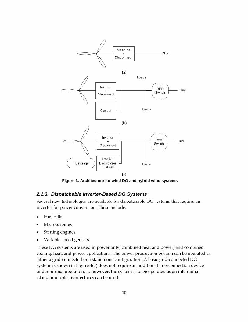
2.1.2. Wind DG Systems Wind DG systems can be distinguished from the large wind turbine farms (which typically feed the utility transmission or the subtransmission system) based on their lower rating and interconnection point. Wind DG systems usually consist of a single small turbine system that is connected to the distribution grid. Such a system can consist of either a directly connected machine or a machine connected to the grid through an inverter. Most installed systems use the direct machine interconnection topology [Smith] shown in Figure 3(a). A DER Switch is not required in this case as the wind power is used only in grid‐connected configurations.
A wind‐diesel hybrid configuration can be used for applications where power needs to be continuously provided in a standalone configuration. When wind turbines in standalone systems produce excess power, the power is dissipated through the use of dump loads.
By using an inverter‐based interconnection with the grid, the need for dump loads in the wind‐diesel system can be eliminated by sending the excess power to the grid. Most wind‐diesel hybrids today are not grid‐connected systems. However, if grid connection is a possibility, the DER Switch can be used to provide backup power to loads in wind‐diesel system shown in Figure 3(b). A configuration that is of more recent interest is the wind‐hydrogen hybrid system shown in Figure 3(c). The hydrogen can be used as a storage medium or as a source of hydrogen for other uses. When the wind power is low, the hydrogen can be converted back to electricity. The speed of the DER Switch in this application primarily affects the power quality in the standby electrical loads.
Machine+
DisconnectGrid
(a)
Inverter+
DisconnectGrid
Genset
DERSwitch
Loads
Loads
(b)
Inverter+
DisconnectGrid
InverterElectrolyzer
Fuel cell
DERSwitch
LoadsH 2 storage
(c) Figure 3. Architecture for wind DG and hybrid wind systems
2.1.3. Dispatchable Inverter-Based DG Systems Several new technologies are available for dispatchable DG systems that require an inverter for power conversion. These include:
• Fuel cells
• Microturbines
• Sterling engines
• Variable speed gensets
These DG systems are used in power only; combined heat and power; and combined cooling, heat, and power applications. The power production portion can be operated as either a grid‐connected or a standalone configuration. A basic grid‐connected DG system as shown in Figure 4(a) does not require an additional interconnection device under normal operation. If, however, the system is to be operated as an intentional island, multiple architectures can be used.
10
11
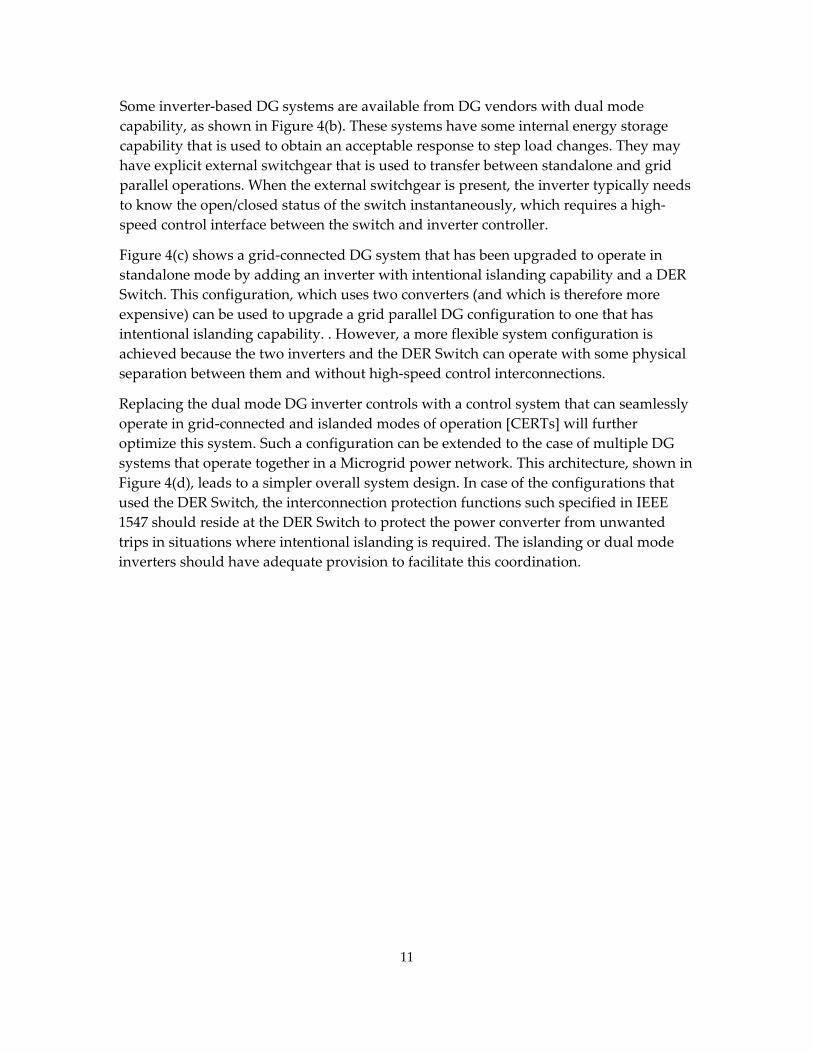
Some inverter‐based DG systems are available from DG vendors with dual mode capability, as shown in Figure 4(b). These systems have some internal energy storage capability that is used to obtain an acceptable response to step load changes. They may have explicit external switchgear that is used to transfer between standalone and grid parallel operations. When the external switchgear is present, the inverter typically needs to know the open/closed status of the switch instantaneously, which requires a high‐speed control interface between the switch and inverter controller.
Figure 4(c) shows a grid‐connected DG system that has been upgraded to operate in standalone mode by adding an inverter with intentional islanding capability and a DER Switch. This configuration, which uses two converters (and which is therefore more expensive) can be used to upgrade a grid parallel DG configuration to one that has intentional islanding capability. . However, a more flexible system configuration is achieved because the two inverters and the DER Switch can operate with some physical separation between them and without high‐speed control interconnections.
Replacing the dual mode DG inverter controls with a control system that can seamlessly operate in grid‐connected and islanded modes of operation [CERTs] will further optimize this system. Such a configuration can be extended to the case of multiple DG systems that operate together in a Microgrid power network. This architecture, shown in Figure 4(d), leads to a simpler overall system design. In case of the configurations that used the DER Switch, the interconnection protection functions such specified in IEEE 1547 should reside at the DER Switch to protect the power converter from unwanted trips in situations where intentional islanding is required. The islanding or dual mode inverters should have adequate provision to facilitate this coordination.

Inverter+
DisconnectGrid Microturbine
Loads
(a)
Grid
Load
Dual mode Inverter +
DisconnectMicroturbine
(b)
GridDER Switch
Load
Inverter+
DisconnectMicroturbine
Dual Mode Inverter+
Battery
(c)
GridDER
Switch
LoadIslanding inverter +
Disconnect Microturbine
Islanding inverter +
DisconnectMicroturbine
...
(d)
Figure 4. DG architecture with dispatchable sources: (a) Grid parallel configuration (b) Dual mode inverter with grid parallel and stand alone capability and do not require additional DER Switch (c) Upgrade of grid parallel configuration to provide backup (d) Multiple DG configuration that requires additional DER switch.
12

13
2.1.4. Machine-Based DG Systems These are the most common form for DG and consist of backup gensets with transfer switches, as shown in Figure 5(a). The DG unit can be used for backup power and, occasionally, to reduce peak demand on the utility grid. The generator is typically off and needs to be started before the transfer switch can operate. Hence, there is no benefit to making the transfer operation very fast.
Figure 5(b) shows a DG configuration where the generator normally operates in parallel with the grid. The interconnection is achieved with traditional CBs. In some large DG applications, the switches may consist of a generator paralleling CB and a grid paralleling CB. Replacing a standard switch with a DER Switch as shown in Figure 5(c) for utility paralleling will be easier if the DER Switch can be certified to meet standardized grid interconnection requirements. The ability of the DER Switch to operate in a standalone manner offers flexibility in the physical location of the switch and the generator.
In the case of induction generator‐based DG, the DER Switch can soft start the generator. This can limit the surge current during startup. Silicon‐controlled rectifier (SCR)‐based soft starters are already used for applications such as wind.
Figure 5(d) shows a traditional synchronous machine DG that can operate as an intentional island. In such an application, an explicit generator paralleling switch and a utility paralleling switch are required to feed the critical loads. Figure 5(e) shows the same configuration where the utility paralleling switch is replaced by the DER Switch. The benefit of the DER Switch in this case is the ability to rapidly disconnect from the grid when grid starts to experience poor power quality. This can be used to reduce the time period when the load experiences an interruption.
2.1.5. Fast Fault Disconnection Performance In creating the design of the distribution system, the designer forecasts the loads expected on the feeder and builds a buffer or safety factor into the initial design. As the loading increases, the circuit interruption devices on the feeder operate closer to their rated values and gradually eliminate the buffer between the actual and rated load. Introducing DG can offset some of the loading on the distribution feeder. However, heavily loaded feeders may not be able to handle the additional fault current contribution from machine DG resources. In this case, additional fault current limiting equipment needs to be in place to connect any DG into the feeder. An advantage of changing to a DER Switch as in Figure 5(c) is that it can operate rapidly. The capability of the semiconductor‐based switches can be used to limit peak fault current and decouple the effect of large generator X/R ratios. In distribution systems where the fault current contribution is a concern, the DER Switch can provide a zero fault current contribution interconnection. The advanced signal processing capability of the DER Switch controller can be used to rapidly determine power flow magnitude and direction. This capability can be used to coordinate with high‐speed utility equipment. The fast
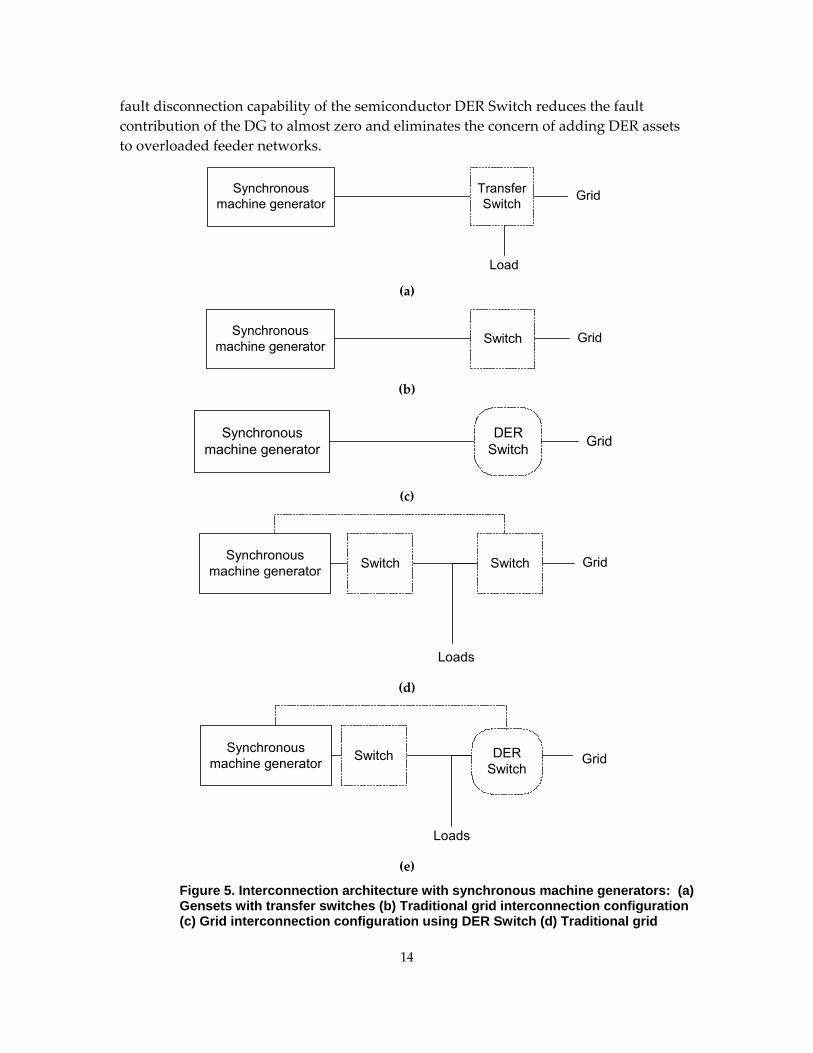
fault disconnection capability of the semiconductor DER Switch reduces the fault contribution of the DG to almost zero and eliminates the concern of adding DER assets to overloaded feeder networks.
GridTransferSwitch
Synchronousmachine generator
Load (a)
GridSwitchSynchronousmachine generator
(b)
GridDERSwitch
Synchronousmachine generator
(c)
Grid
Loads
Synchronousmachine generator SwitchSwitch
(d)
DERSwitch
Grid
Loads
Synchronousmachine generator Switch
(e)
Figure 5. Interconnection architecture with synchronous machine generators: (a) Gensets with transfer switches (b) Traditional grid interconnection configuration (c) Grid interconnection configuration using DER Switch (d) Traditional grid
14

interconnection configuration with islanding capability (e) Grid interconnection configuration with islanding capability using DER Switch.
2.1.6. High-Speed Power Quality Performance The unique capabilities of the DER Switch to address concerns of DER interconnection from the utilityʹs point of view is discussed above. This switch can also provide additional service to the load from the point of view of power quality. Loads have been supplied from uninterrupted power supply (UPS) systems in situations that require high power quality. DG and backup generation are typically considered to be slow sources of energy that can come online while the UPS provides the short term‐time critical‐power backup in a configuration shown in Figure 6(a). A configuration for providing power to critical loads in conjunction with DER with energy storage is shown in Figure 6(b).
GridtransferSwitch Loads
DG /Back up genset
UPS
(a)
GridDERSwitch
Loads
DG withEnergy storage
(b) Figure 6. Power system configurations to feed loads with high power quality requirements: (a) Traditional UPS configuration (b) Configuration based on DER Switch.
Traditional CBs with relay packages to monitor power quality used in this type of configuration cannot meet the requirements of standards like the Computer and Information Technology Industry Council‐Computer and Business Equipment Manufacturers’ Association (ITIC‐CBEMA) curve or SEMIF47. The switch controller should be able to detect the power quality disturbance and react to it by opening the switch on a subcycle basis. The high‐speed capability of the DER Switch lends itself to be compatible with these requirements. Hence, the DER Switch can replace the functionality provided by the UPS and its associated switchgear. The power flow in the DER Switch in this case is the difference between the loads and the DG system. Thus, the
15

16
DER Switch configuration offers lower overall system cost, improved grid power quality, and lower system‐wide energy loss.
2.1.7. Microgrid Power Networks As DG systems become more common, there will be increasing use of Microgrid power networks to take better advantage of their capabilities. A possible architecture for a Microgrid is shown in Figure 7. The power network within the Microgrid can range from the conventional radial distribution to more a complex distribution network. The DER Switch would be an appropriate choice for the utility interconnect device between such a network and the utility grid. Because the power quality within the Microgrid is a function of the speed of the DER Switch, the DER Switch can help accelerate the acceptance of Microgrids. The islanding inverters and machines in the Microgrid should be able to coordinate the interconnection protection functions with the DER Switch. For example, an IEEE 1547 frequency event should cause the DER Switch to open rather than cause the individual DER devices to shut down. Similarly, an under‐ or overvoltage event should open the DER Switch before the individual DER devices are opened. Additional study is needed to ensure that the Microgrid’s components can operate safely as an intentional island to ensure all individual DER devices are coordinated to prevent conflicts. A class of pre‐selected DER Switch “plug and play” compatible devices could be created in the future to eliminate the need for extensive design studies for compatible devices. However, the operation of the overall Microgrid and its individual devices is beyond the scope of this report.

Loads
Synchronousmachine generator
Grid
Loads
Loads
Inverter+
Disconnect
PV
Islanding inverter+
DisconnectMicroturbine*
Islanding inverter+
DisconnectMicroturbine*
PowerNetwork
Switch
DERSwitch
Loads
Loads
Machine+
Disconnect
Figure 7. DER switch architecture to connect a Microgrid power network to the grid
2.1.8. Conclusions Switch configurations currently offer basic solutions for DER interconnections. A DER Switch design better addresses some of the issues and concerns for the interconnection, especially for intentional islanding. In addition, a DER Switch can be used to improve the services provided by the DER in terms of load power quality and reduction in fault current contributions by using a semiconductor‐based DER Switch. These improvements are provided through the combination of the DER Switch’s advanced controller and higher switching speeds. In general, the DER Switch lends itself to more advanced power network architectures.
2.2. DER Switch Specification and Design A DER interconnection with the grid that meets the application requirements described in the previous chapter requires a flexible hardware concept. A traditional implementation of such a concept will involve switch hardware, voltage and current sensing devices, protective relays, a controller with diagnostic and monitoring functions, a communications processor, power supplies, and other components. A DER Switch aggregates the control functions in a DSP. The hardware flexibility is retained in the DER Switch with the additional capability of replacing a CB with solid‐state switches. In the case of a solid‐state switch, additional breakers are used to obtain high fault
17
18
1.
2.
3.
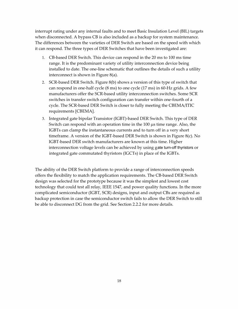
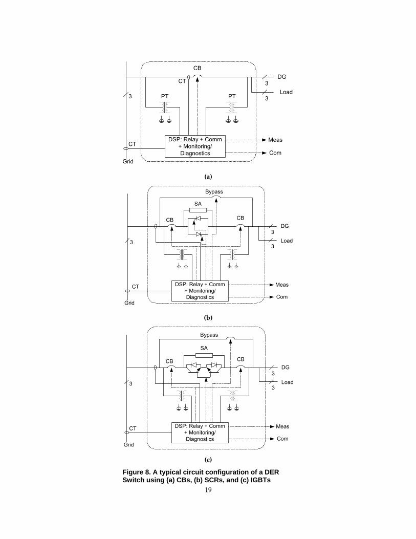
interrupt rating under any internal faults and to meet Basic Insulation Level (BIL) targets when disconnected. A bypass CB is also included as a backup for system maintenance. The differences between the varieties of DER Switch are based on the speed with which it can respond. The three types of DER Switches that have been investigated are:
CB‐based DER Switch. This device can respond in the 20 ms to 100 ms time range. It is the predominant variety of utility interconnection device being installed to date. The one‐line schematic that outlines the details of such a utility interconnect is shown in Figure 8(a).
SCR‐based DER Switch. Figure 8(b) shows a version of this type of switch that can respond in one‐half cycle (8 ms) to one cycle (17 ms) in 60‐Hz grids. A few manufacturers offer the SCR‐based utility interconnection switches. Some SCR switches in transfer switch configuration can transfer within one‐fourth of a cycle. The SCR‐based DER Switch is closer to fully meeting the CBEMA/ITIC requirements [CBEMA].
Integrated gate bipolar Transistor (IGBT)‐based DER Switch. This type of DER Switch can respond with an operation time in the 100 μs time range. Also, the IGBTs can clamp the instantaneous currents and to turn off in a very short timeframe. A version of the IGBT‐based DER Switch is shown in Figure 8(c). No IGBT‐based DER switch manufacturers are known at this time. Higher interconnection voltage levels can be achieved by using gate turn-off thyristors or integrated gate commutated thyristors (IGCTs) in place of the IGBTs.
The ability of the DER Switch platform to provide a range of interconnection speeds offers the flexibility to match the application requirements. The CB‐based DER Switch design was selected for the prototype because it was the simplest and lowest cost technology that could test all relay, IEEE 1547, and power quality functions. In the more complicated semiconductor (IGBT, SCR) designs, input and output CBs are required as backup protection in case the semiconductor switch fails to allow the DER Switch to still be able to disconnect DG from the grid. See Section 2.2.2 for more details.
CB
DSP: Relay + Comm+ Monitoring/Diagnostics
DG
Meas
CT
PT PTLoad
3
3
ComGrid
3
CT
(a)
Grid
CB
SA
Bypass
CBDG
Meas
3
CT
Load3
3
Com
DSP: Relay + Comm+ Monitoring/Diagnostics
(b)
Grid
CB
SA
Bypass
CBDG
Meas
3
CT
Load3
3
Com
DSP: Relay + Comm+ Monitoring/Diagnostics
(c)
Figure 8. A typical circuit configuration of a DER Switch using (a) CBs, (b) SCRs, and (c) IGBTs
19

2.2.1. DER Switch Specification The proposed DER Switch is physically independent from the DER and hence is DER technology neutral. All decisions for control and protection are based on local information; use of overall power system information is only for enterprise energy management as indicated in the power network block diagram in Figure 9. The DER Switch is considered appropriate for a power system that can intentionally island. Adequate compatibility is expected in terms of ratings of the loads, DER devices, and the DER Switch that are connected to the electrical network. This specification section is universal for the various pieces of interconnection equipment. The switching technologies under consideration are based on:
• CBs
• SCR‐based static switches
• IGBT/IGCT‐based static switches
For prototype purposes, only a CB‐based DER Switch will be constructed. This will be a low‐cost prototype where all the control algorithm performance can be evaluated. The control is compatible with that for the SCR or IGBT based switches. Consequently, the CB‐based DER Switch can verify all DER Switch control algorithms. This specification covers the configuration of the DER Switch that connects an area EPS to a single DER or to a Microgrid power network as shown in Figure 9.
PCC SG PD L
M&D
PR
M&D
PC
LC
GEPM
M&D
PC
LC
GEPM
L
WEB
Area ElectricPower System
Flexible DER Interface System
Power Network AwareDER Asset
MTR MeterPCC Point of common couplingSG Switch gear (Power module)PD Power distribution (Power module)PR Protective relaying (Control module)M&D Monitoring & dispatch (Comm. module)PM Prime moverGE DER GeneratorPC Power converterLC Local DER device controlL Loads
MTR
Figure 9. DER power network block diagram indicating the target role of the DER Switch (dashed blue line envelope)
20
21
The DER Switch can also accept and provide switching commands. Hence more generalized configurations, such as a transfer switch, can be created out of a DER Switch. The DER Switch design does not incorporate DG protection. This keeps the switch fully independent of the DER technology. The DER Switch will be suitable for three‐phase, three‐wire (ABC) + ground, or four‐wire (ABCN) + ground circuits. The DG connected in the DER power network can be single phase or three phase.
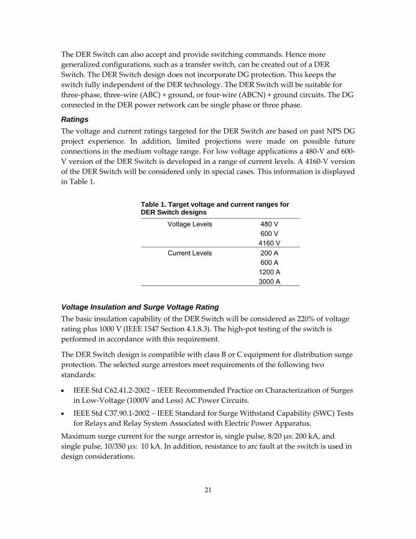
Ratings The voltage and current ratings targeted for the DER Switch are based on past NPS DG project experience. In addition, limited projections were made on possible future connections in the medium voltage range. For low voltage applications a 480‐V and 600‐V version of the DER Switch is developed in a range of current levels. A 4160‐V version of the DER Switch will be considered only in special cases. This information is displayed in Table 1.
Table 1. Target voltage and current ranges for DER Switch designs
Voltage Levels 480 V 600 V 4160 V
Current Levels 200 A 600 A 1200 A 3000 A
Voltage Insulation and Surge Voltage Rating The basic insulation capability of the DER Switch will be considered as 220% of voltage rating plus 1000 V (IEEE 1547 Section 4.1.8.3). The high‐pot testing of the switch is performed in accordance with this requirement.
The DER Switch design is compatible with class B or C equipment for distribution surge protection. The selected surge arrestors meet requirements of the following two standards:
• IEEE Std C62.41.2‐2002 – IEEE Recommended Practice on Characterization of Surges in Low‐Voltage (1000V and Less) AC Power Circuits.
• IEEE Std C37.90.1‐2002 – IEEE Standard for Surge Withstand Capability (SWC) Tests for Relays and Relay System Associated with Electric Power Apparatus.
Maximum surge current for the surge arrestor is, single pulse, 8/20 μs: 200 kA, and single pulse, 10/350 μs: 10 kA. In addition, resistance to arc fault at the switch is used in design considerations.

22
Fault Current Rating The fault current seen at the DER Switch depends on the short circuit ratings of the local EPS. The fault current interrupt rating will be in a range from 18 kA to 85 kA (at 600 V) for the CB‐ and semiconductor‐based DER Switch designs. The surge operating current rating for the semiconductor device is limited to twice nominal current for 10 s.
Frequency The nominal frequency considered is 60 Hz. The system hardware design is consistent for use with 50‐Hz and 60‐Hz grids.
Switching Speed The range of switching speeds considered will depend on the type of DER Switch technology. Switching speed is defined as the clearing time for a disturbance that can affect loads based on the CBEMA/ITIC power quality definitions [CBEMA]. The semiconductor‐based DER Switch will have the capability to respond in 4.2 ms. This is more than four times faster than the CBEMA/ITIC or SEMIF47 requirements. The CB‐based DER Switches will be within a 20−100 ms range for trip speed.
EMI Compliance with EMI – IEEE Standard C37.90.2 is at the overall DER Switch package level. The enclosure and filters should be able to withstand electrical fields of 35 V/m at a range of 15 cm from the exposed surface of the enclosure in the radio frequency range (25–1000 MHz). The DER Switch and the DER Switch controls will not change states when subjected to such fields.
Environment The design will target −20oC to 50oC operational temperature range and a −40oC to 70oC storage temperature range. Cooling will be natural or forced air‐cooling. The air for cooling will be filtered when necessary. A fully sealed system is used for the naturally cooled switches. Elevation is 1000 m above sea level. Derating will be required above this elevation.
Enclosure Rating and Electrical Connections Minimum NEMA 3R (indoor/outdoor) rated enclosure is used. The power connections are:
• Three‐phase grid side connections
• Three‐phase load side distribution panel connections
• Three‐phase DG connections
• Neutral – option for neutral feed through for four wire systems
• Ground – Solid grounding of enclosure. Feedthrough of ground wire to load/DER.
Construction standards within the enclosure are consistent with guidelines from UL 1741 and UL 508A.
23
Life Expectancy Target life expectancy of the unit is 10 years or longer. With CB‐based DER switches significantly longer life expectancies are possible. Subcomponents may require replacement or overhaul after a fixed number of operations. Yearly inspections are expected for the components.
Measurements Current transformers (CTs) will meet relay and metering grade standards so that they have high accuracy and do not saturate when exposed to large fault currents. The CTs will have a 5A nominal secondary rating.
Potential transformers (PTs) selection will require a 120‐V nominal secondary rating.
Current sensors for semiconductor based DER Switches will use sensors with greater than 10 kHz bandwidth.
2.2.2. DER Switch Control Requirements The control of the DER Switch is designed to be switch technology neutral. In addition, the same control system can be used for a DER Switch that implements the actual switch function with a CB, thyristor (SCR), or IGBT based switch technology. For the purposes of the prototype, the CB‐based switch technology has been selected.
The high‐speed capability of the IGBT switch and DSP allows clearing times in the range of fractions of a millisecond. This allows the capability of zero fault current contribution to the grid and the possibility of operation with network protectors that need zero reverse power flow. When the DER Switch is used in combination with DER assets that can seamlessly pick up loads in cases of grid disconnection, high power quality is available to the load. For less demanding applications, the same prototype design with CB switches can be used.
The control functions are based on the raw analog and digital inputs to the DSP. A small amount of filtering is provided for EMI and noise rejection. Additional control inputs are possible through the Human Machine Interface (HMI). Control functions evaluate these inputs to achieve interconnection protection, to meet the IEEE 1547 standard requirements, and to evaluate ambient power quality. DG protection is left to the DG controls and is not included in the DER Switch. The DSP controller provides on‐off commands for semiconductor switches and control of the CBs within the DER Switch. Additional spare analog and digital outputs can be used for overall power system integration. The evaluated values of the control algorithms are available through the HMI for energy management functions.
DER Switch State Machine The state machine controls the operation of the DER Switch. The primary operating states of the DER Switch are to connect the grid and DER or to stay disconnected. A number of the other control states are used for the startup sequence, faults, and bypass operations. Figure 10 shows the state diagram for the DER Switch controller, which is

used for the various DER Switch options (CB, SCR and IGBT). Modes of operation of the DER Switch can be selected to obtain different behavioral characteristics within the operating states. The behavior of the DER Switch when operating in the controller states is described below.
Off State: The DER Switch following power‐up and reset of the controls is considered to be the Off state. The DSP controller conditions for the Off state are: no faults are latched, all alarms are enabled, snaplog is enabled, all semiconductors are disabled, and all discrete outputs are off. Mode settings can be changed only in this state. Any CB that stays closed in this state triggers a fault. A startup sequence can be initiated from this mode. The unit can transition to the Manual Bypass state if the Manual mode is set.
Startup On StatesOff
entry/ Open all CBsentry/ Open IGBT switch
DisConnect
entry/ Open IGBTswitchentry/ Open Bypass CBentry Disconnect timer
do/ Grid PQ monitordo/ DG status monitor
exit/ Conection check
Connect
entry/ Close IGBT switchentry/ Open Bypass CBentry/ Connect light ON
do/ Grid PQ monitordo/ EPS Fault monitordo/ island monitordo/ DG status monitor
exit/ Connect light OFF
Start
Reset command[faults cleared]
Stop command
Fault
Fault
Testentry/ Self testentry/ Dischrg IGBToff
Fault
AutoBypassentry/ Close Bypass CBwait/ TDentry/ Open IGBT switchentry/ Connect light ONdo/ DG status monitor
exit/ Connect light OFF
ManualBypass
entry/ Connect light ON
exit/ Connect light OFF
ManualTransition(Ext. In 4)
Faultentry/ Open IGBT switchentry/ Open all CBsentry/ Fault indicator ON
exit/ Fault indicator OFF
Stop command
Prechargeentry/ Precharge
exit/ Close CBs A,B
Fault
Figure 10. State diagram for the DER Switch Manual Bypass State: The condition for this state is similar to the Off state except that the Bypass CB can be closed. A fault is triggered if the Input and Output CBs (Figure 11) are closed in this state. There is no event‐related change of state in this mode.
Test State: A start command in the Off state initiates the transition to the Test state. The motorized input and output CBs should be ready to close (closing is done in the Precharge state). The grid and DER side voltages are monitored to see if they are in the
24

nominal range and PLL lock occurs on at least one side. If voltage is absent from both sides, the unit goes to fault; otherwise, the unit goes to the Precharge state.
Precharge State: The clamp capacitor is charged up to the peak AC line to line voltage in this state. The precharge contactor is closed. The input and output circuit breakers are closed if the clamp voltage is above a minimum level. The precharge contactor is opened after this. A fault is generated if the clamp voltage is too low or if the input and output circuit breakers fail to close.
Disconnect State: In the Disconnect state, the DER Switch checks to see if DER is present in the system. The DER status is obtained with a bit that is set high when DER is present or low when DER is absent. If it is present and the synchronization functions evaluate to True, the DER Switch transitions to the Connect state. If no DER is present, the controller checks to see if the DER side represents dead bus (27R) and the DER Switch transitions to the AutoBypass state.
Grid
CB In
SA
CBBypass
CBOut
DG
Meas
3
CT
Load 3
3
Com
DSP: Relay + Comm+ Monitoring/Diagnostics
Vg Vdg
Is
Ir
Is
Figure 11. One-line schematic of the DER Switch showing sensor locations
If there is a request to shut down the DER without de‐energizing the loads (bit set through the supervisory control system while in Disconnect state), the synchronization functions are evaluated. When the synchronization functions are true, the DER Switch transitions to the AutoBypass state. This feature should be used only if there is an external supervisory controller for the DG‐DER switch system, which will ensure that the DG status is off within a short duration after reaching the AutoBypass state.
25

26
Connect State: In the Connect state, the DER Switch checks for power quality, anti‐islanding, other IEEE1547 functions, and fault events. If any of these events are true, the DER Switch transitions to the Disconnect state. If the DER is shut off (DER status is absent), the DER switch transitions to the AutoBypass state.
AutoBypass State: In the AutoBypass state the DER Switch checks to see if the DER is reconnected to the system. The DER Switch operates like a regular CB in this state and does not open in case of power quality problems. If the DER status indicates that it is going to be reconnected, the DER Switch transitions to the Connect state. The DER status will probably be updated before the reconnection by the Supervisory control system. If the supervisory control is not in place, the AutoBypass state is not used.
If the DER Switch entered the AutoBypass state because of a Request for DER shutdown, the control system should ensure that this request does not persist for a long time. The controller should time out this request and indicate a warning in case the request continues to persist.
Fault State: If there are faults, the DER Switch can shut down rapidly into a safe state. In this state, all CBs are open and the phase IGBTs are off. The clamp IGBT’s operation is independent of whether the DER Switch is in the Fault state. The DER switch enters on initial power‐up in this state. The semiconductor‐based (IGBT or SCR) designs have extra input and output CBs to provide backup protection in case the semiconductor‐based switch fails.
DER Switch Operating Modes The following operating modes are provided within the DER Switch state machine:
Auto/Manual Mode: The mode can be set only remotely using the HMI. The change of mode can only be made only in the Off state.
Local/Remote Mode: The mode can be set remotely with the HMI. The setting of the mode to local will disable all other commands from the HMI except stop or Local/Remote mode change. The Remote mode will disable Start or Reset commands from the DER Switch Local interface. Stop command can be given locally or remotely in all situations.
High‐Speed Power Quality Mode: The mode can be set remotely with the HMI when the DER Switch is in the Off state. The setting of this mode to False will disable the high‐speed CBEMA/ITIC evaluation, high speed anti‐islanding, and instantaneous overcurrent functions.
Positive/Absolute Synchronization Mode: Absolute synchronization looks at the absolute values of the phase, frequency, and voltage magnitude errors. Positive synchronization mode allows the switch to close only when these errors are positive.
27
Test Mode: This mode can be set remotely with the HMI. The change of mode can be made only in the Off state. In this mode, the DER Switch operates normally except that the physical switches are always off.
Analog and Digital I/O The internal current sensors within the DER Switch can measure both AC and DC current with a high bandwidth. The external analog inputs for current measurement assume the use of 5 Arms secondary CT. Analog inputs for grid and DG AC voltage measurements are made with 120 Vrms nominal at the PT secondary. The one‐line schematic indicating analog signal sensor locations is shown in Figure 11. Sixteen DSP board analog channels that are directly available for high speed sampling are used in the controller.
The analog inputs are:
• Current sensor – (Is) phase A, B, C, N (4x)
• External CTs – (Ir) phase A, B, C (3x)
• Grid side sensing – (Vg) phase A, B, C (3x)
• DG side sensing – (Vdg) phase A, B, C (3x)
• DC clamp voltage common and differential (2x for IGBT switch only)
• Control voltage sensing (V24) (1x)
Two spare multiplexed analog input channels are available for application‐related requirements.
Digital inputs to the DSP are optoisolated and debounced. The primary inputs from the DER Switch controller are: Start, Enable (used as stop), and Reset. The following are application‐related digital inputs and can be interfaced with 24‐V DC relay coils that can be externally energized:
• Trip signal where a high signal indicates an external command to the DER Switch to transition to the Disconnect state if the system is in the Connect or Bypass states.
• Two additional spare channels are available and can be configured either as active high or active low.
Additional internal digital input signals are used to monitor the IGBTs’, the CBs’, and the contactors’ fault and status indicators.
The 10‐mA digital outputs of the DSP are optoisolated. Additional interposing relays with Normal Close/Normal Open or Form C dry contacts with surge protection are used to provide isolation and surge ratings. The two application‐related contacts available externally are the “Connected or Disconnect status” of the DER Switch and an “auxiliary switch” output. The auxiliary switch output can be used to open any CB in series with the DER Switch or trigger another DER Switch or CB to obtain a transfer switch system configuration.

28
Optional analog 0−5‐V output voltage signals are available on the DSP controller board. The signals are centered at 2.5 V; 5 V represents the maximum rated output capacity. The analog output signals implemented in the DER Switch are three‐phase real and reactive power. Two additional spare channels can be used for the application‐related signals. If signals are to be used outside the DER Switch, an isolation amplifier should be used for galvanic isolation and protection of circuits.
Relay Functions The relay functions implemented in the DER Switch based on a survey of requirements from DG projects are listed in Table 2 Additional functions are available for monitoring and diagnostics. Warning message and activation thresholds are also provided.
Table 2. The relay functions implemented in the DER Switch
ANSI# Function Notes 25 Synchronism check
27/59 Under- and overvoltage Including the 27R and 59N functions 50/51 Overcurrent Instantaneous and time coordinated; with residual
current option (50G) 81O/U Frequency Consistent with requirement in Table 5
32 Reverse Power Three phase and per phase directional power/VAR option
Most of the relay functions trigger a transition to the Disconnect state. Exceptions are the 25 and 27R functions that are used as enable signals for the DER Switch to reconnect. The relay functions are provided with options to enable each algorithm independently.
Synchronization check This algorithm is calculated in the Disconnect state. This function checks to verify that the voltage amplitude (for all three phases), frequency, and phase angle are within an acceptable window to allow the DER Switch to close. Other DER Switch control functions may also need to be true to enable the closing. The switch in the DER system is closed only when it is in Auto mode (Section 2.2.2.2) and if the synchronization enable is valid and the reconnection enable (Section 2.2.2.20) is true.
There are two modes for the synchronization function:
• Absolute mode – represents synchronization when voltage, frequency, and phase error magnitudes are small.
• Positive mode – represents synchronization when frequency and phase error are small positive values. This would prevent any power surge during synchronization that can cause any fast reverse power flow function to trip.
The voltage magnitude and phase are compared at the high speed interrupt service routine (ISR) rate of the DSP. This ensures that any sudden jump in voltage or magnitude on either side of the DER Switch does not cause any false synchronization.
29
Dead bus reclosing relay This function is provided in the DER Switch so it can black start the loads connected to the DER side of the switch, when there is no DG connected to the system. This assumes that there is additional DER protection equipment, which disconnects the DER from the loads. A voltage threshold and time delay is provided for coordination. The dead bus relay checks to verify that closing occurs only under a dead bus condition (voltage is below threshold on all three phases) and when DER status is Off.
Under- and overvoltage The voltages on the grid and DER side are monitored to be within acceptable ranges. A threshold and time delay are provided for coordination. Separate voltage thresholds and time delays for the grid side and DER side are provided. An event in the connect state will make the DSP controller transition to the Disconnect state. Any event measured on the DER side when in the Disconnect state results in an alarm to the supervisory control system.
Under- and overfrequency Frequency is measured from the three‐phase voltage measurement on the grid and DER side. Separate frequency thresholds and time delays are provided for coordination on the grid and DER side. An event in the Connect state will make the DER Switch to transition to the Disconnect state. Any event measured on the DER side when in the Disconnect state triggers an alarm to the supervisory control system.
Phase sequence This functions checks for phase rotation direction, missing phase information or lack of signal on the phase voltage. In addition, this function checks to determine whether the controller’s internal data are synchronized with the grid and DER operating frequencies. An event in the Connect state will make the DER Switch to transition to the Disconnect state. An event in the Disconnect state will prevent the synchronization function from operating.
Overcurrent The DER Switch controller provides both instantaneous and time over current relay functions. Additional neutral and ground time overcurrent relay functions are also implemented. The neutral current function can be used for four wire applications. The current flowing through the DER Switch is measured. The trip threshold levels and time delay before tripping are independently adjustable. The calculations for this algorithm are performed in the Connect state. Any event occurrence makes the controller transition to the Disconnect state.
Reverse power The DER Switch controller evaluates single‐ and three‐phase power flow at the switch and at a remote location. Remote measurement is possible if additional CTs are wired into the DER Switch controller. Independent thresholds are available for switch and remote reverse power. The power measurement is compared with an adjustable

30
threshold and time delay for coordination. If the power flow crosses the threshold, an event is set. The user can select whether the crossing occurs in the positive or negative direction for the event to occur. An event in the Connect state will cause the DER Switch to transition to the Disconnect state.
Controller digital event In addition to the above relay functions a bit can be set in the DER Switch controller to simulate an event. Also, the external digital input can be used to simulate an event occurrence in the controller.
IEEE 1547 Functions The recently approved IEEE 1547 standard contains control requirements that need to be satisfied for the interconnection of DER to the grid. Other standards such as UL1741 and state standards such as California Rule 21 reflect many of the underlying concerns that are addressed by the IEEE 1547 standard. The DER Switch is designed to be fully compliant with the IEEE 1547 standard and has the flexibility to meet additional requirements. The main control functions required for the DER Switch to meet the IEEE 1547 standard relate to:
• Voltage
• Frequency
• Harmonics
• DC injection
• Anti‐islanding
• Synchronization
• Reconnection.
The details of these control functions are discussed in the following sections.
Voltage function The voltage functions are implemented so that concerns related to the response at the DER interconnection to shallow or deep voltage sags and swells can be type tested and set independently of other under/over voltage relay functions described in Section 2.2.2.7. The nominal settings are listed in Table 3. Voltage levels are based on rms calculations for phases A, B, and C of the grid voltage. The voltage threshold is specified in volts on a 120‐V basis. The values for voltage range and clearing times represent type test values and are not easily modified in the field.
Table 3. Interconnection system response to abnormal voltages
Range Voltage range (% of base voltage)
Clearing time (s)
1 V < 50 0.16 2 50 ≤ V < 88 2.00 3 110 < V < 120 1.00

31
4 V ≥ 120 0.16
Frequency function The frequency function is implemented so that a small frequency swing does not lead to disconnection of the DER from the grid. The nominal settings are listed in Table 4. This function is implemented independently of the under‐ and overfrequency relay functions in Section 2.2.2.8. Frequency is obtained based on internal three‐phase phase locking algorithms. These values represent type test values and are not easily modified in the field.
Table 4. Interconnection system response to abnormal frequencies
Range Frequency range (Hz) Clearing time (s) 1 > 60.5 0.16 2 < {59.8–57.0}
(adjustable set point) 0.16−300 Adjustable
3 < 57.0 0.16
Harmonics monitor The DER Switch by itself does not directly cause harmonic distortion. A small amount of harmonic current will be caused by the control power required by the switch. The on‐state voltage of the semiconductors can lead to less than 0.5% harmonic distortion in the voltage in the IGBT DER Switch. The switch will be able to monitor the ambient voltage distortion and the distortion caused by the connected DER or loads. Harmonics are evaluated on switch current, grid, and DER side voltage. A high level of harmonic distortion is treated as a warning. The distortion level for warning will be based on the DER rating and a typical setting for the total demand distortion would be 5%. The harmonics monitor has not been implemented in the prototype DER Switch.
DC monitor The DER Switch can monitor the DC component of the switch current caused by the connected DER or loads. A high level of DC in the switch current is treated as a warning. The DC current level for the warning can be set based on the rating of the DER connected to the DER Switch [2].
Anti-islanding The anti‐islanding function is evaluated when the switch is in the Connected state. The goal is to prevent islands from forming inadvertently in the power system. The anti‐islanding function within the DER Switch can disconnect the DER from the grid within two seconds of the grid opening, consistent with IEEE 1547. The anti‐islanding function in the DER switch is based on preventing the export of power to the grid, but can allow power to be exported to lateral distribution loads based on remote power measurement. Power flow in the DER Switch is monitored either at the switch or at a remote location if
32
remote CTs are wired into the switch. Power is monitored on both a single‐phase and a three‐phase basis. The three‐phase evaluation of power is performed at high and medium speed. The high‐speed evaluation of power enables the DER Switch to detect reverse power flow and to open a semiconductor‐based switch in less than a quarter of a cycle. The anti‐islanding algorithm is independent of the reverse power relay function described in Section 2.2.2.11. The power threshold level and time delay for opening the switch are adjustable settings on the controller and can be based on the application requirements. The ability to use either the switch power or a remote power measurement for anti‐islanding detection, consistent with IEEE 1547, leads to a greater flexibility to detect islands in a wide range of applications.
Synchronization The level of synchronization that must be achieved before closing the DER Switch is defined by IEEE 1547 through specified maximum deviations in the voltage amplitude, frequency, and phase angle. The synchronization check function of Section 2.2.2.5 is used to implement this function. The window parameters used for the synchronization check function will be consistent with those required by IEEE 1547. The peak switch current after closing is monitored over the next 10 line cycles and is reported as a warning in case it exceeds thresholds.
Reconnection The DER Switch is enabled to reconnect only after all enabled events are cleared. The events considered are relay functions or IEEE 1547 and power quality events. A minimum reconnection time is imposed after grid conditions are restored to normal and after the switch turn‐off transition. The reconnection time is adjustable based on application requirements and is consistent with IEEE 1547.
Power Quality Functions The DER Switch can rapidly disconnect from the grid if it senses any power quality disturbance. The power quality evaluations made with the DER Switch are for the ITIC/CBEMA curve and the SEMIF47 envelope of the grid voltage. The algorithm is evaluated only when the DER Switch is in the connected state and the calculations are made for all three‐phase voltages.
Voltage power quality events are classified into high‐, medium‐, or low‐speed events. The high‐speed events are evaluated at the highest signal sample rate and the others are evaluated at 1/16th of the sample rate. Time delays obtained with filter functions are used to obtain a system response that approximates the curve in Figure 12. Default settings would correspond to the ITIC/CBEMA curve. The response of the DER Switch will be to go from a Connect state to a Disconnect state in the case of a power quality event.

Figure 12. The ITIC/CBEMA and SEMIF47 curve (red)
Energy Management Interface The energy management interface in the DER Switch is provided by the NPS SmartView® supervisory control and data acquisition (SCADA) system of hardware and software that provides the capability to monitor and control geographically distributed assets from anywhere in the world. There are many disparate monitoring solutions, but SmartView specializes in aggregating data from many sources and providing access to those data in a flexible, standards‐based way. The key capabilities of the SmartView SCADA solution are:
• Fleet and local monitoring of geographically distributed assets
• Flexible graphical interface connectivity, including Web browser
• Real‐time data and alarms using the openness, productivity, and connectivity Data Access standard
• Historical data, events, and trending with the open data base connectivity standard
• Execution of supervisory control
• Automated alarm reporting via email and pager
• Automated data reporting
The SmartView system is also used as an Engineering HMI for commissioning and testing the prototype switch. The internal control variables in the DER switch control DSP can be monitored in the SmartView remote terminal unit (RTU) with a one‐second update rate. The SmartView HMI can also be used to setthresholds, time delays, and
33

control modes and parameters. The organization of the SmartView SCADA system that will be used for the DER switch is illustrated in Figure 13. When necessary, the SmartView RTU can also use the Modbus communication protocol to monitor the DER. Details of the SmartView system are provided in Appendix C.
DG
SmartView®RTU
Grid DER SwitchDER Switch
ModBusModBus
Internet/LANEnterprise
EMS
Figure 13. SmartView energy management interface
2.2.3. Design Summary The DER Switch design has been targeted to provide high performance, high reliability, maximum flexibility, and a low system cost. The use of the IGBT technology along with the advanced control capability of the DSP results in a very high‐speed switching capability. Integration with the SmartView SCADA can help the user realize the full range of benefits from a flexible DER utility interface switch.
2.3. Component Selection The DG‐grid interconnection switch developed in the DER Switch program is intended to offer high‐performance features. The IGBT‐based DER Switch configuration has higher performance and a higher cost than the SCR and CB switches for DER interconnections. This section describes the design of the IGBT‐based DER Switch, but the other switch designs can to a large extent be obtained by simplifying this high‐performance design. The prototype that has been constructed is the low‐cost, CB‐based design.
2.3.1. DER Switch Circuit Topology The switch circuit shown in Figure 14 can be divided into three main subsystems:
• IGBT switch
• Voltage clamp circuit
• CB and power connection assembly
34

Circuit Breaker and Power Connection Assembly
IGBT Switch
CBOUTPUT
CBBYPASS
A
B
C
CBINPUT
FromGrid
To DG,Load
Voltage Surge Suppression
Figure 14. Circuit configuration of the DER switch
The selection of standard commercial components for subsystems leads to a lower system cost. The integration of these subsystems into the DER Switch is designed to minimize parasitic parameters, leading to a very high system efficiency and reliability. For a CB‐based DER Switch the circuit of Figure 14 is replaced with a single CB.
Semiconductor Circuit Interrupter The typical commercially available IGBT Switch module has unidirectional voltage blocking and current turn‐off capability. The DER switch requires switches with bidirectional voltage and current blocking capability. , which can be obtained by arranging switches and diodes in a number of ways (see Figure 15). Any failure in the semiconductor device is protected by the opening of the input and output CBs in Figure 14.
35

(a) (b)
Figure 15. Topology options for the bidirectional switch
The topology (a) of Figure 15 shows a bidirectional switch made from two single IGBT modules. In this case, a single gate driver could be used to drive both IGBT gates as the emitter terminal is common to both switches. The anti‐parallel diodes of the IGBTs tend to have higher on‐state voltage drop than do line frequency diodes. Hence, the circuit in topology (a) can have higher losses in an application where the switching frequency is very low (see Table 5).
Table 5. Conduction characteristics for two topology options
Vona (V)
Rona (mΩ)
IGBT 2 3.9 Anti-parallel diode 1 1.9
Diode 0.75 0.2 Topology(a) 3 5.8 Topology(b) 3.5 4.3
aOn‐state voltage drop of semiconductor devices at maximum junction temperature (IGBT module 125oC, Diode module
150oC)
The bidirectional switch of topology (b) has lower cost because only one IGBT is required. The on‐state conduction drop would correspond to that of three devices (IGBT and two diodes).
Voltage Surge Suppression Circuit The IGBTs have the inherent capacity to turn current off at high speed. The typical rate of change of current (di/dt) of IGBTs in power converter applications is in the range of tens of kA/us. The inductance of the power line to the DER Switch connected is highly application dependent. In addition, the transformers and DER equipment can have high inductance. A typical value for the transformer leakage inductance is about 5% of its base impedance. Similarly, machine DGs can have high values of subtransient
36

inductance. These inductances, coupled with the di/dt of the IGBT, may lead to very large voltage spikes across the IGBT during its switching transient.
A number of methods can be used to mitigate the voltage spike. Figure 16 shows a schematic of possible configurations of voltage suppression circuits that can be used in the DER Switch for three‐phase applications. Other methods of single‐phase surge suppression are possible between the input and output of the switch. However, the three‐phase approach provides protection against all modes of voltage surges. These can include input‐to‐output, line‐to‐line, and line‐to‐ground voltage surge modes.
CB
ABC
(a) (b) (c) Figure 16. Voltage suppression topologies for three phase applications: (a) Voltage surge suppressors, (b) crowbar circuits, (c) clamp snubber circuits Voltage surge suppressors are commonly used in applications to protect equipment from voltage spikes. The suppressor should be compatible with the IEEE C62.41.2‐2002 and IEEE C37.90.1‐2002 standards. The surge arrestor can be of different varieties: a spark gap type device, a metal oxide varistor, or a semiconductor‐based arrestor. These devices have different characteristics for response time, surge energy, and voltage breakover. Despite these differences, the surge suppressor’s voltage limits all share a strong dependence on their operating current as well as a limited number of operations. Unlike the voltage surge suppressor devices, the crowbar or a clamp‐type voltage limiting arrangement is suitable if repetitive operation of the voltage suppression device is expected.
The crowbar option is shown in Figure 16(b). The crowbar circuit is turned on when an overvoltage is detected. The thyristors connect the inputs to ground, connecting the source of high voltage to ground. This immediately lowers the voltage and the resulting overcurrent causes the CB to open, which in turn disconnects the source of the overvoltage from the protected sections of the circuit.
A third option for surge voltage suppression is a capacitor clamp snubber. In this case if the energy behind the overvoltage source is limited, the clamp capacitor voltage starts rising in response to the overvoltage condition. The capacitor can be sized to keep the voltage rise to be within safe limits for typical overvoltage expected because of on‐off
37

38
operation of the DER Switch. Any energy added to the clamp capacitor is dissipated in the discharge resistor in parallel with the capacitor.
For the DER Switch, a combination of the metal oxide surge suppressor and the clamp snubber circuit is required to prevent the overvoltage spike. The crowbar circuit is not used so as to prevent unnecessary operations of the CB.
Circuit Breaker Configuration The CB arrangement in the DER Switch consists of input, output, and bypass sections. The input and output CB can be used to isolate the DER Switch with galvanic isolation. These CBs also enable the user to turn off the large fault current in case of a fault within the DER Switch. The opening or closing of the CB is performed under the DSP control to prevent surge current in the clamp capacitor snubber circuit. A fault within the DER Switch causes the input and output CB to trip. As most on‐off operations of the DER Switch are accomplished with the IGBT switch, the number of operations of the CB is expected to be low.
The bypass CB is used to power the loads in case the semiconductor part of the DER Switch needs to be serviced. The bypass CB is also used if no DER is connected to the output for an extended time. This reduces power loss that would otherwise have been dissipated in the semiconductor devices.
The input, output, and bypass CBs can be disconnected and locked in the racked out position. The control power for the DER Switch can also be visibly locked in the off position. This provides the visible disconnect requirement for utility connection [IEEE 1547]. The CB arrangement is simplified to that of a single device for the CB DER Switch. The single CB can be used in the position of the IGBT to obtain the visible isolation and manual bypass capabilities.
2.3.2. Component Selection Guidelines Semiconductor Components Selection There are several possible configurations for implementing the IGBT‐based DER Switch. To select the configuration to be constructed, a spreadsheet‐based design tool was created to allow for the quick calculation of the candidate circuit’s power dissipation, junction, and heat sink temperatures under rated steady‐state and transient overload conditions and overall efficiency based on different IGBT and diode options. Based on the system voltage rating of 480 Vrms and the desire to be able to handle the largest interrupting voltages possible, only 1700‐V devices were considered.
The spreadsheet used the expressions of Equations 1 and 2 to compute the IGBT and diode power dissipation.
PIGBT_rated = Ipeakπ Vceo +
12⎝⎜⎛
⎠⎟⎞Ipeak
2 2 rCEsat (1)

39
Pdiode_rated = Ipeakπ VTo +
12⎝⎜⎛
⎠⎟⎞Ipeak
2 2 rT (2)
The transient surge power is computed in the same manner; however, the current Ipeak is substituted with the surge current Isurge defined by Equation 3.
Isurge = ⎝⎜⎛
⎠⎟⎞
1 + Surge%100 Imodule (3)
Steady‐State Temperatures
Steady‐state temperatures for the IGBT, diode, and heat sink are determined for rated and surge current conditions. The methods are the same, except for the current values selected for the calculation. The rated conditions use the average rated current, Imodule and the surge current Isurge. The heat sink temperature is computed using
Ths ~ Tref = Ndevices (PIGBT + Pdiode) Rra + TA (4) where Ndevices is the number of devices within the module, Rra is the thermal resistance between the heat sink thermal reference and the ambient, and TA is the ambient temperature.
The thermal reference is assumed to be at the same temperature as the heat sink. In reality, this temperature will be slightly higher than the actual heat sink temperature.
The heat sink and semiconductor module manufacturer provide transient thermal data for the heat sinks used with the IGBT modules and Rra can be obtained from these data with
Rra = Σi [1,6] Ri (5) The diode and IGBT junction temperatures are obtained with
Tdiode = Pdiode Rjr + Tref (6) TIGBT = PIGBT Rjr + Tref (7)
Transient Temperatures
The transient thermal model provided by Semikron consists of a thermal impedance Zth,
Zth = Σi=[1,6] Rthi(1‐e‐t/τi) (8) This impedance can be considered as a series string of parallel connected thermal resistances and capacitances. The thermal resistance is Rthi and the thermal capacitance is Ci = τi/Rthi. Using the electrical analog model the power dissipation maps to current and temperature drops or rises map to voltage drops or rises.
Assuming an initial steady‐state temperature rise for the thermal circuit of T0, the transient thermal rise expression is
Tr(t) = T0 + Σi=[1,6] ( )P Rthi – Rthi/ΣRthi T0 ( )1 – e‐t/τi (9)

40
The heat sink temperature is the heat sink thermal reference transient temperature rise plus the ambient temperature. The diode and IGBT temperatures are the heat sink thermal reference temperature plus the respective transient temperature rise. For the surge calculation, t is the surge time and T0 is the rated steady‐state temperature rise.
We used these calculations methods to calculate the conduction losses and transient temperatures for the IGBT switch. The DER Switch specifications require a 100% surge capacity for only 10 seconds, but to allow the DER switch to be more flexible for utility coordination purposes, the ability to carry a 400% surge for several cycles was an important design goal.
The IGBT modules include an integrated gate drive circuit that incorporates hardware overcurrent protection. In the DER Switch application, both IGBTs should be turned on at the same time. The IGBT module gate drives can be modified to disable their internal shoot‐through protection mechanisms. Taking into account the desire to use an IGBT module for its greater current carrying capacity, the internal target of a 400% surge rating, and the need to disable the shoot‐through protection of the gate drive circuit, the device selected is a 750‐A, 1700‐V rated half‐bridge IGBT module.
Several possible line‐frequency rectifiers would be possible candidates for the diode portion of the DER Switch. To reduce the conduction losses as much as possible to allow the maximum amount of fault current capacity, the largest diode option, an 1800‐V, 700‐A diode half‐bridge, was selected.
Assuming a 60oC ambient temperature for the DER Switch cabinet interior the IGBT, diode, and heat sink temperatures for steady‐state operation, after a 100% surge for 10 seconds and after a 400% surge for two cycles (32 ms) are listed in Table 6. The estimated efficiency will be 98.7%.
Table 6. Estimated operating temperatures Steady State (oC) After 10 s, 100%
surge (oC) After 32 ms, 400%
surge (oC) IGBT Junction 92.2 112.1 125.2 Diode Junction 90.3 101.7 105.1
Heat Sink 84.2 91.3 94.7
Clamp Selection The DER Switch system has two protective systems. The first provides protection from large external transients such as a lightning strike. This mode of protection includes surge arrestors connected at the power terminals of the DER Switch. The second operates when the DER Switch interrupts current and protects the DER Switch components (as well as externally connected components) from the voltage transient created by the stored energy in the system’s inductance. This mode of protection includes a snubber clamp circuit.

41
Surge Arrestor The surge arrestor is selected based on the design specifications that require the DER Switch design to be compatible with class B or C equipment for distribution surge protection. This requirement is satisfied by using surge arrestors that meet the requirements of the following standards:
• IEEE Std C62.41.2‐2002 – IEEE Recommended Practice on Characterization of Surges in Low‐Voltage (1000 V and Less) AC Power Circuits.
• IEEE Std C37.90.1‐2002 – IEEE Standard for Surge Withstand Capability (SWC) Tests for Relays and Relay System Associated with Electric Power Apparatus.
The maximum surge current for the surge arrestor is, single pulse, 8/20 μs: 200 kA, and single pulse, 10/350 μs: 10 kA.
The selected surge arrestors are DIN rail mounted for ease of construction and contain an integral switch that provides a way to indicate that they have failed because of an excessive surge, preventing further DER Switch operation.
Snubber Clamp Circuit The snubber clamp circuit operates each time the DER Switch interrupts current. When the DER Switch is closed, the flowing current stores energy in the series inductance of the transformers, conductors, DER, motor loads, etc. When the DER Switch opens quickly (as it is designed to do), this fast interruption of current creates a high voltage across the device that stops the current flow.
Circuit Breaker Selection Based on the DER Switch specifications, a molded‐case CB was specified. This is a 250‐A, 600‐Vac rated CB with a Underwriters Laboratory/Canadian Standards Association interrupting capacity of 65 kArms under 480 Vac. The selected breaker has adjustable trip settings for long time, short time, and instantaneous trips and includes two auxiliary contacts. One contact will provide a status input to the DSP and the other will be used to turn off the shunt‐trip coil once the breaker opens. To allow a separate mechanism for opening the breakers, a 24‐Vdc shunt‐trip will be included to allow for a second layer of control. The shut trip is also triggered when any fault is detected in the semiconductor switch. These faults include failure to open when commanded to open and failure to close when commanded to close. The opening of the input and output CBs protects the semiconductor switch in a fault situation. The bypass switch can then be used to continue providing grid power to the loads.
In addition to the basic CB, a motor operator will be added to allow the DSP to operate the CB. A racking and draw‐out kit will be added to provide a visible and lockable disconnect.

Pre-charge The clamp capacitor needs to be pre‐charged before the main CBs close to limit the amount of current that would otherwise flow through the clamp diodes. One portion of the clamp pre‐charge circuit is shown in Figure 17.
R
C
R
F
F
Figure 17. Clamp capacitor pre-charge circuit
Because the DER Switch may be energized from either the grid or DER side, the pre‐charge circuit must allow the clamp capacitor to be pre‐charged from either side. The circuit in the previous figure is duplicated to achieve this goal.
Before closing the main CBs, the DSP will close the pre‐charge contactors to allow the clamp capacitor to charge through the pre‐charge resistor. To reduce cost, the clamp is charged from only two of the three phases. The pre‐charge resistors are connected through a fuse to their corresponding phase clamp diodes.
The pre‐charge contactor needs to be a four‐pole contactor with a 480‐Vac and at least a 2‐A make rating. The DSP will operate this contactor through an interposing relay so the pull‐in current required by the contactor will not affect the 24‐V power supply bus.
Discharge Every time the DER Switch opens, the clamp circuit will absorb energy by charging the clamp capacitor. This energy will need to be discharged to allow the clamp to safely absorb the energy of the subsequent DER Switch operation. The clamp capacitor is discharged through the discharge circuit of Figure 18. This circuit consists of an IGBT, resistor, and free‐wheeling diode. This circuit is the same configuration as is commonly used in non‐regenerative machine drives for DC bus braking choppers.
42

R
C
Figure 18. Clamp discharge circuit
For safety purposes, a normally closed relay is placed in parallel with the IGBT. This relay is opened by the DSP energizing its coil under normal operation. Should the control power be lost, this relay will close and discharge the clamp capacitor. Because the clamp must not be externally energized when the discharge relay is closed, a permissive relay will be added to prevent the clamp from being energized. When the discharge relay’s coil is energized, the discharge contacts open and a clamp permissive relay coil is energized. This relay allows the pre‐charge contactor and the main CBs to be closed. Because the clamp’s negative bus likely will be several hundred volts from ground, a separate isolated supply is needed for the permissive relay coil. This supply is operated from the 125‐Vdc control power bus in a similar manner to the other low‐voltage dc supplies.
Selecting a peak clamp current of approximately 5 A and assuming a peak voltage of 1700 Vdc, suggests a resistance of 330 Ω. Factoring in the re‐closing time, the resistor will dissipate an average of 162 W. The selected 330‐Ω, 220‐W resistor will allow a worst‐case current of 5.2 A, which is within the ratings of the safety discharge relay.
Because the peak current will be approximately 5 A, the key driving specification for the brake chopper will be the voltage rating of 1700 V. This selected device is a 75‐A, 1700‐V IGBT bridge pole consisting of two IGBTs and two anti‐parallel diodes. For the purposes of the clamp operation, the upper IGBT will be disabled by connecting its gate terminal to its emitter terminal.
The power dissipated by the chopper IGBT while the clamp capacitor is being discharged is an average of 6.9 W during the clamp operation. On average, it will dissipate approximately 380 mW. Allowing a 150ºC maximum junction temperature, this means that the maximum Rja is 235ºC/W, so minimal heat sinking will be required for thermal purposes and the heat sink can be selected for mechanical mounting ease.
Control Power
43
44
Normally, the control power would be derived from the grid side terminals, since these would typically be energized; however, in the DER Switch applications, this is not always the case. Therefore, the control power must be obtainable from either the grid or the DER side terminals. This requirement is achieved by using two isolation transformers with one transformer connected to the grid side terminals and one transformer connected to the DER side terminals.
The secondary outputs of the transformers are rectified and connected to a common unfiltered 125‐Vdc bus. This bus is used to power the CB’s motor operators and the low‐voltage power supplies for the DSP, gate drive, control relays, and contactors. The low‐voltage power supplies are specified to have a universal input so they can accept the unfiltered dc input.
The enclosure has two cooling fans to exchange the air inside the cabinet with cooler outside air. The enclosure fans are controlled by a 50oC snap switch. One fan is powered off the grid side terminals and one fan is powered off the DER side terminals. Three fans are mounted on the heat sinks to cool the semiconductor devices. These fans are controlled by a relay that is closed when the DSP closes the DER Switch. When the DER Switch is open, there is no need for the cooling fans to run because the semiconductor junctions will not be generating additional heat. This controlled operation of these fans improves the DER Switch’s efficiency, reducing the cooling requirements for the enclosure.
The shunt‐trips are triggered by either the DSP or the Emergency‐Stop button. Because a continuously depressed E‐stop button could overload the shunt‐trip coils, each shunt‐trip coil is wired in series with a switch that opens when the shunt‐trip has activated the CB. When the CB trips open, the shunt‐trip coil will automatically turn off.
Sensor Selection PTs will be used to measure the voltages and will provide a 120‐V nominal output. The current for the external input will be measured with standard current transformers that are rated to meet relay and metering grade levels of accuracy and provide a 5‐A nominal secondary current.
The outputs of the PTs and CTs will be connected to the analog signal conditioning board (ASCB) that will provide the appropriate burden and attenuation required by the DSP’s analog inputs. The phase and neutral currents are measured with LEM current sensors. While the dc clamp’s chopper gate drive will measure the clamp’s voltage and independently operate the clamp chopper without action on the part of the DSP, it will still be important for the DSP to be aware of the status of the clamp. This is achieved through two methods. First, should the clamp chopper gate drive detect a fault, this error will be digitally communicated to the DSP. Potential faults include that the clamp bus voltage has exceeded 1400‐Vdc or that the IGBT is overloaded as indicated by the loss of saturation. The second method for monitoring the clamp voltage is for the DSP to directly measure this voltage through an analog voltage sensing channel on the ASCB.

45
2.3.3. Evaluation of Project Objectives DER Switch and Project Costs The DER switch is fully engineered to meet the requirements of the IEEE 1547 standard. An initial analysis to verify the impact of the interconnection cost of the DER switch was conducted based on past NPS project experience. This indicated that a separate interconnection switch is not economically feasible at low power levels. This resulted in the range of power for the DER switch to be as specified in Table 1. The cost of the prototype CB DER Switch is comparable to current solutions; the costs of the prototype semiconductor‐based switch are higher. However, semiconductor‐based switches have greater power quality and fault current limiting capabilities. These costs are also expected to drop with production quantities. In addition, significant nonrecurring engineering costs of $30K−$40K were estimated for the semiconductor‐based DER switch. The breakdown of the equipment cost is shown in Table 7. The costs correspond to the prototype DER Switch for the rating specified in Appendix A. The CB‐based DER Switch at the prototype level has costs that are comparable to current solutions. The cost of the SCR assembly with its gate drive, protection, and fans is about $3K lower than the IGBT DER Switch costs. The control costs of the DER Switch (except the sensors) are invariant with the switch rating. The prototype estimates are rough ones for the SCR‐based DER Switch. Further study of the cost reduction that may be achieved for production‐level quantities of the DER Switch is recommended.
Table 7. Bill of major materials and costs
Component IGBT DER Switch CB DER Switch
Quantity Extended cost ($)
Quantity Extended cost ($)
IGBT + gate drive + heat sink
3 4,995.00
Diodes 3 555.00 Clamp diodes 7 175.00
Clamp capacitor 2,600.00 Clamp IGBT 833.00
Fans 3 878.00 1 293.00 Misc. hardware 3000.00 3000.00 Circuit breakers 3 4,680.00 1 1,560.00
DSP + Signal conditioning boards
2,300.00 2,300.00
Control power 850.00 850.00 Misc. Controls 2,500.00 2,500.00
Total $23,366.00 $10,503.00
46
The projected engineering costs for DER interconnection are assumed to be based on the additional time that would be required for the interconnection to be certified as compliant with IEEE 1547 and to complete fault studies based on the interconnection. Project experience indicates that about one‐fourth of the time spent on a DG project is related to studying the system and applying an interconnection configuration. The main project studies that would be required for the DER interconnection are related to the local grid architecture, the ability of the interconnection equipment to meet the local standards, and the power flow and voltage impact and fault studies. Of all these, the DER Switch design can be used to mitigate the interconnection standards, architecture, and fault studies. About $10K can be saved based on a simplified interconnection study. This can vary widely based on projects. An additional $10K in design savings can be assumed for IEEE 1547 compliance.
Reliability Projections A preliminary estimate of the reliability of the DER Switch is mainly limited by that of the control boards in the switch. In case of the semiconductor based switches, the gate drives’ circuits add an additional penalty to the DER Switch’s reliability. The operations and maintenance (O&M) cost was estimated by using the main component’s probability of failure and its replacement cost with the following number of failures per 10E‐06 h: CB = 1.3, IGBT = 2.5. The IGBT based switch has a higher O&M cost because of a higher failure rate of electronic devices. The data for this analysis were obtained from O&M Cost Analyses for NREL WindPACT Drive Train Configurations, prepared for NPS by TIAC LLC, Cambridge, Massachusetts.
Additional Performance Objectives The DER Switch controller provides a detailed fault and alarm levels that can be used to track the cause of damage. However, to obtain the MTTR of less than two hours, a spare DER Switch is assumed to be available on site. The level of spare availability depends on the criticality of providing power the loads and to keep the DG running. In cases where operating the DG is not critical, the DER Switch could be operated in bypass mode for an extended time.
The control of the DER switch is based on a single DSP that incorporates a wide range of measurement, protection, and communication functions. The DER Switch controller is capable of all three‐phase voltages on both the grid side and the DG side. This enables robust synchronization algorithms that can reliably close the switch with minimal surge after closing. In addition, the positive and absolute synchronization options can be used in cases where there are restrictions of initial power flow direction immediately after the switch closing. The anti‐islanding algorithm used in the DER switch is based on reverse power, which is acceptable to most utilities. The ability to perform the anti‐islanding

47
based on remote current measurement provides greater flexibility in using the DER Switch for the detection of unintentional island situations.
2.3.4. Conclusions This section describes a semiconductor prototype DER Switch design from which SCR and CB prototypes can also be created. Use of standard commercial power component selection leads to lower system costs than designs that use custom modules. This section outlines IGBT DER Switch design and identifies the control requirements and the resulting controller design. Photographs of a 200‐A, 480‐V CB‐based switch can be found in Appendix B. The next section describes the test results and analysis of the switch. The comparison of the program goals and the DER Switch design is summarized in Table 8. Photos of the DER switch in Appendix B show the switch controller and the switch cabinet toward the end of fabrication. Overall, the major program goals for the DER Switch can be met. Section 3 of this report details this prototype’s ability to meet the program’s objectives of IEEE 1547 compliance, anti‐islanding, resynchronization, and response time.
Table 8. Summary of the DER Switch program goals and design evaluation
Requirement CB SCR IGBT IEEE 1547 compliance Yes Yes Yes Prototype initial cost $11k $20k $23k 30% Reduction in equipment costs − (82%) (109%) 50% Reduction in project engineering costs
25% 30% 50%
MTTF > 80 k h 256k 60k 55k Anti-islanding and resynchronization Yes Yes Yes Enterprise energy management interface Yes Yes Yes Response time 20−100 ms 8−17 ms < 2 ms Clamps instantaneous currents No No Yes Market share Majority Minority N/A

48

49
3.0 Project Outcomes This section outlines the tests completed to verify the DER Switch prototype meets its stated functionality and specifications. The tests were divided into several sections and were performed at NPS’s test facility laboratory in Waitsfield, Vermont, and NREL’s DERTF near Boulder, Colorado.
The tests included general commissioning followed by the various operational tests. The general commissioning tests were conducted to ensure the switch’s manufacturing integrity. The operational tests concentrated on confirming the operation of the various control algorithms, including the prototype’s performance, relay functions, IEEE 1547 functions, and power quality functions.
Some of the tests were feasible to perform at NPS’s test facility; others were performed at NREL’s DERTF. Section 3.1 shows the tests performed and their locations. Sections 3.2 and 3.3 outline the general test setup and test procedure, respectively, that took place throughout the testing effort. In‐depth test setup, procedures, and results can be found in an independent document (NPS Test Plan) that was submitted to NREL under this contract. The tests performed at NREL by NREL staff also followed a detailed test plan that was shared with NPS.
3.1. Test List and Location A commissioning test was performed on the prototype unit before any functional testing was conducted. This included a wiring check, cooling system check, high pot test, internal power supply test, and DSP power‐up and checkout. The prototype unit passed all these tests.
Table 9 lists the tests and the locations where they were completed. These are indicated by the check [ ] marks.
3.2. Test Setup This section describes the tests that were performed on the prototype unit internally at NPS and externally at NREL.
3.2.1. Internal Testing, NPS’s Test Facility The test setup of the DER Switch at NPS’s test facility consists of two power converters (PR4 and PR5) that are connected as shown in Figure 19. These are three‐phase inverters and their outputs are at 208Vacl‐l. Transformers T3 and T4 are used to step up the voltage to 480 Vacl‐l. The inverter PR4 is used to emulate the grid and the unit PR5 is used to emulate the DER asset. The operation of the DER Switch can be tested in several scenarios using this setup. The 1:1 delta‐wye transformer (Tx) can be used to test various grounding and neutral schemes.

50
Table 9. Test list, status, and location performed
Location NPS (Waitsfield, VT) NREL (Boulder, CO)
Test List Test status Performance test Relay function tests Voltage tests
Frequency tests
Phase sequence test
Current tests
Set and digital even trip tests
IEEE1547 tests Overvoltage test
Undervoltage test
Over- and underfrequency tests
Synchronization test
Reverse power test
Unintentional islanding test
Open phase test
Reconnect following abnormal disconnect test
CBEMA
Because of the controller setup for the PowerRouter inverters, the grid inverter has independent control of each phase; the DG inverter has three‐phase controllable outputs. The loads of the PowerRouter inverters are adjustable and changed accordingly to obtain desired power flow.
Test instruments required:
• Two PowerRouter inverters
• Two 3/5/12kW Resistive load banks
• Three Y:∆ transformers
• Six CBs
• One HMI computer
• A data acquisition system.

Z Z
DERSwitch
CB3G25A
CB4G25A
T3 T4
CB4
PR4Emulate
Grid
PR5Emulate
DG
3/5/12kW
3/5/12kW
CB5
480V UtilitySW7
HMIComputer
208V 208V
Comm.PowerRouter operation
DER Switch testing
NN
N480V
480V
Tx
Remote CTNot yetinstalled
Existing
CB3PRG32A
CB4PRG20A
3+G,#10AWG
Figure 19. NPS’s setup for testing the DER Switch in the Waitsfield test facility
3.2.2. External Testing, NREL’s Distributed Energy Resource Test Facility All testing performed at NREL’s DERTF was done by injecting signals directly to the controller signal conditioning boards. This practice is commonly referred to as secondary injection testing. Most digital controller devices do not directly measure line voltage and current conditions. Rather, they measure scaled versions of line conditions with scaling being accomplished through PTs and CTs. These transformers convert high primary voltage and current levels to values that are much more appropriate for digital sensing and processing applications. NREL’s DERTF has equipment that can precisely generate secondary injection level signals. This was used to perform testing and enabled sophisticated testing without having to actually cause real line or generator faults, and eliminated the risks to personnel and equipment.
The secondary injection test sets can generate voltage and current signals with precise control over magnitude, frequency, and phase. The CMA256‐6 has four independently controllable voltage sources and the CMS156 has three. Each unit is synchronized to the other and is controlled by the same software via a laptop computer. The DER Switch has six voltage input signals; three on the utility side and three on the DG side. The DER Switch controller senses voltage via line‐to‐neutral connected, 2.31 ratio PTs. This ratio translates to a 120‐V line to neutral secondary signal for 277‐V line to neutral conditions. Three of the CMA256 voltages were connected in wye to the DG side PT secondaries. Likewise, the three CMS156 voltages were connected to the utility side PT secondaries.
51

52
1.
2.
To simulate the nominal 480‐Vac bus conditions, 120‐Vac line to neutral was supplied by the test sets. To simulate faulted conditions, PT ratio‐scaled perturbations around nominal bus conditions were applied to the PT secondaries. By monitoring breaker status and the state of the voltage outputs when the breaker tripped, the performance of the DER switch was evaluated.
To prevent reverse energizing of the primary bus, PT circuits were disconnected from the test circuit voltages by removing the fuses that completed the circuit path.
Test instruments included:
• Omicron CMA256‐6 secondary injection test set
• Omicron CMS156 secondary injection test voltage amplifier
• Yokogawa PZ4000 power analyzer
3.3. Test Procedure This subsection outlines the general procedure taken to test the DER switch prototype. Specific event settings are included in Section 3.4 Test Results, where those values are compared against the actual response.
General procedure taken:
The DER Switch unit was connected to the PowerRouter inverters and loads; one inverter and load pair emulated the grid and another pair emulated the DG source. (Refer to Figure 19 for the test setup.) The PowerRouter inverters were energized at nominal operating condition (480VAC,LL, 60Hz). The synchronization windows (voltage magnitude, frequency, and phase) were configured accordingly to allow the switch to close when the grid and DG voltages are synchronized. Note: For the tests performed at the NPS test facility, the PowerRouter inverters were used as the grid and DG sources. The Omicron device was used to create the voltage and current excitation for the tests at NREL. Secondary injection method was used at the PT secondary level. Proceeding steps written below were similar for both cases.
Only the event functions under test were enabled; all other event functions were disabled. The event settings were adjusted to the appropriate values, which. will not be included in this section. In some cases, the setting values are being limited by the PowerRouter inverters’ capability. For those situations, the settings were adjusted to be within the inverters’ limitation and the prototype unit was tested for the event instead of actual magnitude. An example of this situation is IEEE 1547 overvoltage or overfrequency. Further tests to verify the actual magnitude were performed by NREL at the DERTF.
53
3.
4.
The inverters were adjusted accordingly to create an event. For example, the voltages were increased from the nominal operation to a level above the overvoltage setting. To perform the magnitude test, the inverter parameters were adjusted in small steps. The value at which the DER Switch tripped was recorded. To perform the time test, the inverter parameters were adjusted with a step change. The time from when the parameter was changed to when the digital command was sent to the CBr, and to when the CB completely opened were recorded.
These steps were repeated several times at different magnitude and time settings. They were also repeated for the event functions for which the DER switch was designed.
3.4. Test Results This section details the results for all the tests performed on the DER Switch. In general, three test setpoints for each magnitude and trip time test were chosen. These setpoints were different enough to verify that the function tested responded as expected at any condition. Some of the setpoint pairs listed in the results table may not have the time response indicated because those settings were not tested for the trip time.
The discussions about the results are categorized into three subsections: relay functions, IEEE 1547, and CBEMA. Results from NREL’s tests are also included here and the differences between the results from NPS and NREL will be addressed.
3.4.1. Performance Tests The DER Switch was subjected to some general commissioning tests, which include wiring and quality check. The purpose of these tests is to ensure that the components are electrically and correctly connected before the switch is energized for other proceeding tests. High pot test was also done with measuring the current through the insulation at high voltage. This is to detect weak spots in the insulation that may cause failure. The cooling system in the prototype unit provides air cooling for the cabinet if the temperature exceeds 40°C. All these tests were passed and the tested functions operate as expected.
The performance of the internal 24‐Vdc power supply was checked out as shown in Figure 20 and Figure 21. These figures show the transient and steady‐state response, respectively, of the voltage and current of the 24‐Vdc power supply. The scope channels are as listed below:
• Scope channel 1: Input voltage
• Scope channel 2: Output voltage
• Scope channel 3: Input current
• Scope channel 4: Output current.
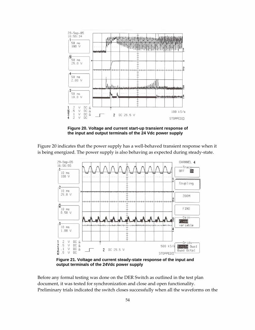
Figure 20. Voltage and current start-up transient response of the input and output terminals of the 24 Vdc power supply
Figure 20 indicates that the power supply has a well‐behaved transient response when it is being energized. The power supply is also behaving as expected during steady‐state.
Figure 21. Voltage and current steady-state response of the input and output terminals of the 24Vdc power supply
Before any formal testing was done on the DER Switch as outlined in the test plan document, it was tested for synchronization and close and open functionality. Preliminary trials indicated the switch closes successfully when all the waveforms on the
54

55
grid and DG sides are synchronized within a set window defined by the user. The switch closing action was successful with minimal surge between the two source terminals.
Table 10 indicates the closing and opening times of the CB. This was tested at NPS and the values agree with NREL’s observations. They are also in line with the expected response speed estimated during the design stage. Throughout the testing the closing and opening times of the CB were consistent with the data shown in this table.
Table 10. Operation times of DER Switch Observed time
(ms) Closing time 100 Opening time 80
Figure 22 shows the connection transition of the CB. When the switch is not connected, the waveforms at the grid and DG side are distinctive, since the DG inverter was not generating a perfect sine wave because of the test setup arrangement. However, the voltage magnitudes (in RMS) and frequency were almost identical and are within the synchronization window. The connection transition can be observed in Figure 22. The step signal indicates the command given from the switch controller to the CB. Scope channels 1 and 2 are the grid and DG voltages, respectively. Both voltages will drift and eventually be in phase, which allows the switch to close. When the switch is connected (100 ms after the digital signal in Figure 22), the voltage seen at the grid and DG outputs are equal and the switch allows current to flow, as indicated in Figure 23. The switch disconnection transition, which can be seen in Figure 24, has a similar idea but is opposite to the description provided here.

Figure 22. Waveforms that indicate switch connection transition
Figure 23. Voltage and current waveforms after switch closing
56

Figure 24. Waveforms that indicate switch disconnection transition
Table 11 summarizes the checkout tests performed at NREL to investigate the CB disconnect delay. The average trip delay is 86.3 ms, which is typical for this type of breaker.
Table 11. Breaker disconnect delay determination (test performed at NREL)
Trip command from DSP (sec)
Breaker Opening
(sec)
Trip Time (difference between trip command and
actual breaker opening) (sec)
0.1774 0.2644 0.0870.1678 0.2541 0.08630.182 0.268 0.0860.1773 0.2631 0.08580.1822 0.2687 0.0865
Avg: 0.08632
3.4.2. Relay Function Tests The controls of the DER Switch include functions that emulate ANSI relays and other high‐performance control features. These relay function settings are independent of the IEEE 1547 event settings. The magnitude and time settings of each function are adjustable. Some of the relay functions and IEEE 1547 events may be testing the same parameters. For example, there is an overvoltage test for both. The window of the function not tested must be disabled or widened to ensure that the DER Switch is being tested correctly. After each event that causes the switch to trip, the alarm screen on the EngrHMI and snaplog was checked to confirm the event. This confirms the data
57

58
recorded by the DSP board are correct, which ensures good information from the DER Switch is collected when it is operated in the field.
3.4.3. Voltage tests The purpose of these tests is to verify that the triggering of the undervoltage events occurs at the appropriate voltage level and time delay for coordination. The following voltage tests were performed and repeated for both the grid and DG side independently:
• Undervoltage (27) test
• Overvoltage (59) test
Table 12 indicates that several attempts were made to test the magnitude and time response of the undervoltage relay function. As previously mentioned, the Vtrip information shows the voltage change right before and right after the switch disconnected. These values were visually recorded by the tester on the Engineering HMI measurements screen, which provides an additional error factor. Without taking this into account, the percent error of the voltages right before the switch trips are around 0.86% and 0.51%, with a maximum error in one of the readings of 1.4%.

59
Table 12. Undervoltage relay function test data
Vthreshold
(VAC,LN) Tsetting
(s) Phase Tripped?a Vtrip
b (VAC,LN)
Ttripc
(ms) Grid Side
235 0.2 Phase A 236→234 Phase B Data not recorded Phase C Data not recorded
175 0.2 Phase A No data→173 164+80 Phase B 175.5→174.5 Phase C 175.5→172.7
100 0.05 Phase A 101.4→No data Phase B 100.3→No data Phase C 100.6→No data
175 0.4 Phase A 185→145 200+80 175 0.05 Phase A 185→145 48+80
DG Side 235 0.2 Phase ABC 236.2→230.5 184+80 175 0.2 Phase ABC 176.5→170 175 0.05 Phase ABC 176.5→170 22+80 a indicates that the DER Switch disconnected and the event was displayed on the Engineering HMI. b Indicates the voltage change. The DER Switch disconnected in between this voltage change. c The first number is the DSP processing time and the second number is the circuit breaker disconnection time.
A larger voltage step was used to investigate the trip time. Both the DSP processing time and the CB disconnection time are provided in Table 12. The switch disconnect time is consistent across most of the test setpoints and agrees with the design specification. All the DSP response times observed were shorter than the specified time setting defined. This is an excellent indication that the DER Switch can meet the specified requirement defined by the user; the only limitation is the CB’s response time.
Figure 25 shows the switch response to an undervoltage event. The scope trace shows the surge current in response to the event. This figure illustrates an example of how the time response of each function was tested. The time of the undervoltage is quite clearly seen. The current waveform was superimposed onto the digital signal that commands the switch to open. The delay between the point on the current waveform when the voltage decays and point on the digital signal trace at which the open command is given is the DSP response time. The difference between the time the digital signal changes state to when the current is completely zero is the CB response time. As shown in this plot, the CB response time is approximately 80 ms.

Figure 25. Switch response to a large undervoltage event
The overvoltage responses are summarized in Table 13 and Figure 26. The responses meet the voltage threshold and time settings set to test this function. The largest magnitude error found in the series of tests is 0.5% (for Vthreshold of 260V and Tsetting of 0.2s).
The under‐ and overvoltage tests results confirmed that the controller achieved its software‐programmed functionality.
Frequency tests The purpose of these tests is to verify that the triggering of the over‐ and underfrequency events occur at the appropriate frequency level and time delay for coordination. The following frequency tests were performed and repeated for the grid and DG sides independently: • Overfrequency (81O) test
• Underfrequency (81U) test
60

Table 13. Overvoltage (59) relay function test data
Vthreshold
(VAC,LN) Tsetting
(s) Phase Tripped?1 Vtrip
2 (VAC,LN)
Ttrip3
(ms) Grid Side
260 0.2 Phase A 259.7→265.8 Phase B 259.6→268.2 Phase C 258.7→271.3
180 0.2 Phase A 179.6→186.5 140+80 Phase B 179.8→190.5 Phase C 179.7→189.2
180 0.05 Phase A 179.6→204.6 32+80
DG Side 260 0.2 Phase ABC 259.5→260.6 180 0.2 Phase ABC 179.4→120 167+80 180 0.05 Phase ABC 179.4→180.1 40+80 a indicates that the DER Switch disconnected and the event was displayed on the Engineering HMI. b Indicates the voltage change. The DER Switch disconnected in between this voltage change. c The first number is the DSP processing time and the second number is the circuit breaker disconnection time.
Figure 26. Response of the system to overvoltage event
To test the over‐ and underfrequency relay functions, the frequency of one inverter was adjusted; the other was held constant. Table 14 and
Table 15 show the trip frequency magnitude and response time of the DER Switch.
61
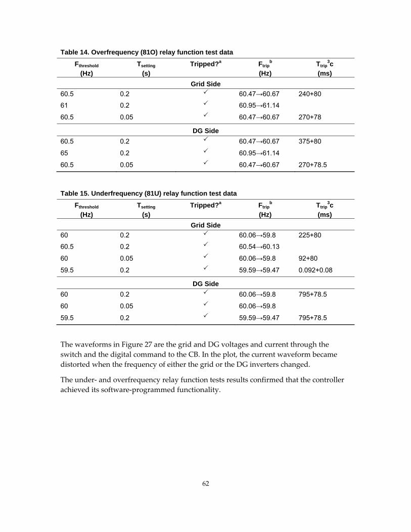
62
Table 14. Overfrequency (81O) relay function test data
Fthreshold
(Hz) Tsetting
(s) Tripped?a Ftrip
b (Hz)
Ttrip3c
(ms) Grid Side
60.5 0.2 60.47→60.67 240+80
61 0.2 60.95→61.14
60.5 0.05 60.47→60.67 270+78
DG Side 60.5 0.2 60.47→60.67 375+80
65 0.2 60.95→61.14
60.5 0.05 60.47→60.67 270+78.5
Table 15. Underfrequency (81U) relay function test data
Fthreshold
(Hz) Tsetting
(s) Tripped?a Ftrip
b (Hz)
Ttrip3c
(ms) Grid Side
60 0.2 60.06→59.8 225+80
60.5 0.2 60.54→60.13
60 0.05 60.06→59.8 92+80
59.5 0.2 59.59→59.47 0.092+0.08
DG Side 60 0.2 60.06→59.8 795+78.5
60 0.05 60.06→59.8
59.5 0.2 59.59→59.47 795+78.5
The waveforms in Figure 27 are the grid and DG voltages and current through the switch and the digital command to the CB. In the plot, the current waveform became distorted when the frequency of either the grid or the DG inverters changed.
The under‐ and overfrequency relay function tests results confirmed that the controller achieved its software‐programmed functionality.

Figure 27. Response of the system to an underfrequency event
Phase sequence test Phase sequence (46) was tested to verify the triggering of an event during abnormal phasing conditions. The phase connection of the grid and DG side were independently swapped. The CB was set to the manual mode and off state and the digital command from the DSP was observed for safety reasons to ensure that the hardware components would not be damaged in this test because of an unintentional connection.
The phase sequence tests were successful. The DSP recognizes the invalid phase connection and the Engineering HMI displayed appropriate FAULT alarms (AC freq grid LO when the grid phases were swapped, AC freq DG LO when the DG phases were swapped). The switch will not close in FAULT state.
Current tests The following current tests were performed:
• Instantaneous overcurrent (51) test
• Time overcurrent (50) test
The purpose of these tests is to verify that the overcurrent event is triggered at the appropriate current level and time delay for coordination. These tests were performed for the switch current measurement locations only.
When this function was first tested, the time response of the instantaneous overcurrent alarm could not be verified, so Table 16 does not include the trip times for the instantaneous overcurrent function test. However, the time responses for the time overcurrent function tests are provided below.
63

64
The initial instantaneous overcurrent test performed indicated that the switch took about 18 cycles to disconnect. In theory, it should take about five cycles, mostly because of the CB, to disconnect because of the processing time that the DSP uses for the different functions. The instantaneous overcurrent calculation is done at the ISR rate; the state machine decisions are made at the Kernel rate. The software has been updated to transfer instantaneous events at the ISR rate to the controller. This test was not repeated at NPS after the software change; however, other similar instantaneous trip tests have been subsequently verified to operate within the expected trip time.
Table 16. Overcurrent relay function test data
Ithreshold (A)
Tsetting
(s) Phase Tripped?a Itripb
(A) Ttrip
c (s)
Instantaneous overcurrent (51)
33
0.002 Phase A 23.15 Phase B 23.41 Phase C 23.7
40
0.002
Phase A 30.5 Phase B 29.98 Phase C 30.5
Time overcurrent (50)
15
0.2 Phase A 14.96 360+80 Phase B 14.29 Phase C 14.58
15
0.05 Phase C 78+80
20
0.2 Phase A 19.81 Phase B 19.84 Phase C 19.69
a indicates that the DER Switch disconnected and the event was displayed on the Engineering HMI. b For the instantaneous overcurrent test, these numbers are the peak of the RMS current. This switch tripped on instantaneous peak that occurs on top of the peak RMS values. For the time overcurrent test, these numbers are the RMS values. c For the instantaneous overcurrent test, the trip time could not be checked out when this test was performed. For the time overcurrent test, the first number is the DSP processing time and the second number is the circuit breaker disconnection time.
Set and digital event trip test Two features—the set and digital event trip functions—were added later to the DER Switch’s set of event functions. The purpose of this test is to verify that the DER switch

65
can perform backup switching operations when commanded to open in coordination with other devices or when commanded to open by system level controllers. The user can set these functions to HIGH and this is registered as an event in the switch controller and trip the unit.
Both functions were tested and passed.
3.4.4. IEEE 1547 Tests The IEEE 1547 standard specifies the voltage ranges and clearing times for overvoltage, undervoltage, overfrequency, and underfrequency events. Specified values are repeated in each section for reference. The controller interface has alarm names assigned to the different voltage ranges in order to simplify the naming convention for these functions. The table that summarizes the IEEE 1547 specifications and results will include these.
The default values in the controller reflect the specification in IEEE 1547. The voltage and frequency settings had to be modified because of the limitation of the PowerRouter inverters. Most voltage settings used for testing purposes were ±5% of nominal voltage; the frequency setting had a ±0.5Hz deviation. At this stage, the DER Switch was tested for its trip setting instead of the exact value of the IEEE 1547 specified settings. The latter was tested at NREL. The results obtained from the tests at NREL are included after the results obtained at NSP, followed by a discussion of the results.
Overvoltage tests These tests were performed to verify that the DER Switch isolates the grid and DG terminals when the overvoltage conditions occur, and determine the magnitude and trip time for each overvoltage function.
Table 17 lists the IEEE 1547 overvoltage ranges and clearing time specifications.
Table 17. IEEE 1547 specification for interconnection response to overvoltages
Voltage Range (% of base voltage)
Clearing Time (s)
Alarm Name
110 < V < 120 1 1547 voltage swell V ≥ 120 0.16 1547 voltage over
The IEEE 1547 overvoltage tests performed at NPS indicated that the voltage magnitude response has a maximum error of 0.5% (Table 18). Table 19 shows voltage trials for the trip time test.

66
Table 18. Switch response to IEEE 1547 overvoltage events Terminal Side Voltage
Settinga (%)
Voltage Settinga (VAC,LN)
Tripped?b Vtripc
IEEE 1547 Voltage Swell Phase A Grid side 105% 291 290.1→298.9 Phase B Grid side 105% 291 289.8→299.4 Phase C Grid side 105% 291 290.2→300.7 Phase ABC DG side 105% 291 289.3→300.6
IEEE 1547 Voltage Over Phase A Grid side 105% 291 290.2→298.6 Phase B Grid side 105% 291 289.7→299.4 Phase C Grid side 105% 291 290.4→300.6 Phase ABC DG side 105% 291 289.6→300.1 a Actual voltage threshold and trip time setting differ from IEEE 1547 specified values due to test setup operating limitation. The more precise voltage setting is VAC,LN is 290.85VRMS. b indicates that the DER switch disconnected and the event was displayed on the Engineering HMI. c Indicates the voltage change. The DER switch disconnected in between this voltage change.
Table 19. Voltage trials for trip time test
Clearing Time Settinga (s)
Alarm Name Voltage Settinga
(%)
Voltage Settinga (VAC,LN)
Tripped?b Ttripc
(s)
1 1547 voltage swell 105 291 1+0.08 0.16 1547 voltage over 105 291 (See note)
Note: The time response was not able to be observed. A summary of the results obtained from the tests performed at NREL is listed in Table 20. These tests closely reflect the method required by IEEE 1547.1, where tests are repeated five times to obtain more accurate results.
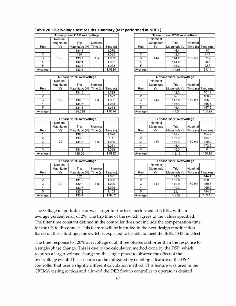
Table 20. Overvoltage test results summary (test performed at NREL)
Run
Nominal Magnitude
(V)Trip
Magnitude (V)Nominal Time (s) Time (s) Run
Nominal Magnitude
(V)Trip
Magnitude (V)Nominal Time (s) Time (ms)
1 134.1 1.079 1 146.4 902 134 1.085 2 142.3 91.13 133.7 1.083 3 144.2 92.24 132.4 1.082 4 144.2 90.15 133.8 1.083 5 146.3 92.3
Average 133.6 1.0824 Average 144.68 91.14
Run
Nominal Magnitude
(V)Trip
Magnitude (V)Nominal Time (s) Time (s) Run
Nominal Magnitude
(V)Trip
Magnitude (V)Nominal Time (s) Time (ms)
1 134.5 1.098 1 142.3 161.22 1.097 2 143 168.73 134.5 1.085 3 143.6 165.94 134.5 1.083 4 146.4 166.35 134.6 1.084 5 146.4 167.5
Average 134.525 1.0894 Average 144.34 165.92
Run
Nominal Magnitude
(V)Trip
Magnitude (V)Nominal Time (s) Time (s) Run
Nominal Magnitude
(V)Trip
Magnitude (V)Nominal Time (s) Time (ms)
1 138.5 1.096 1 148.4 194.22 133.2 1.1 2 150.3 184.33 134.3 1.085 3 149.4 110.24 1.081 4 146.4 172.25 134.2 1.099 5 146.3 93.9
Average 135.05 1.0922 Average 148.16 150.96
Run
Nominal Magnitude
(V)Trip
Magnitude (V)Nominal Time (s) Time (s) Run
Nominal Magnitude
(V)Trip
Magnitude (V)Nominal Time (s) Time (ms)
1 132 1.095 1 144.5 144.42 131.9 1.086 2 150.8 150.33 132.3 1.099 3 146.9 150.84 133.6 1.099 4 149.3 165.65 137.2 1.102 5 151.1 184.8
Average 133.4 1.0962 Average 148.52 159.18
160 ms
160 ms
144
144 160 ms
160 ms
1 s
1 s132
132
132
132
B phase 110% overvoltage
C phase 110% overvoltage
Three phase 120% overvoltage
A phase 120% overvoltage
B phase 120% overvoltage
C phase 120% overvoltage
1 s
1 s
144
144
Three phase 110% overvoltage
A phase 110% overvoltage
The voltage magnitude error was larger for the tests performed at NREL, with an average percent error of 2%. The trip time of the switch agrees to the values specified. The filter time constant defined in the controller does not include the compensation time for the CB to disconnect. This feature will be included in the next design modification. Based on these findings, the switch is expected to be able to meet the IEEE 1547 time test.
The time response to 120% overvoltage of all three phases is shorter than the response to a single‐phase change. This is due to the calculation method done by the DSP, which requires a larger voltage change on the single phase to observe the effect of the overvoltage event. This scenario can be mitigated by enabling a feature of the DSP controller that uses a slightly different calculation method. This feature was used in the CBEMA testing section and allowed the DER Switch controller to operate as desired.
67

68
Undervoltage tests These tests verify that the DER switch isolates the grid from the DG terminals of the switch when undervoltage conditions occur. They also determine the magnitude and time response for each undervoltage function.
Table 21 lists the IEEE 1547 undervoltage range and clearing time specification.
Table 21. IEEE 1547 specification for interconnection response to undervoltages
Voltage Range (% of Base Voltage)
Clearing Time (s) Alarm Name
V < 50 0.16 1547 deep sag 50 ≤ V < 88 2 1547 shallow sag
Table 22 and Table 23 show results obtained for the magnitude and time response of the undervoltage test performed at NPS. The corresponding test performed at NREL is shown in Table 24. Tests performed at NPS show a maximum voltage error of 1%. This, however, does not agree with the results obtained at NREL, which has a larger percent error. As shown in the results for the time response, a larger time deviation was observed at NREL than at NPS for the single‐phase tests. The larger error seen in the single‐phase test can be caused by the selection of the neutral voltage calculation option in the DER switch DSP controller.
The IEEE 1547 under‐ and overvoltage function test results confirmed that the controller achieved its software‐programmed functionality. The accuracy of the trip levels needs to be further refined to meet certification standards. The test results also indicated that the timed delay for the trip function should compensate for the switch opening delays.
Over- and underfrequency tests The frequency tests confirm that the DER switch disconnects the grid and DG connections when an over‐ or underfrequency condition occurs. These tests also verify the trip magnitude and time response for each frequency function.

69
Table 22. Switch response to IEEE 1547 undervoltage events Alarm Name Voltage
Settinga (%)
Voltage Settinga (VAC,LN)
Tripped?b Vtrip
(VAC,LN)
IEEE 1547 Deep Sag Phase A Grid side 95% 263 261.6 Phase B Grid side 95% 263 263
Phase C Grid side 95% 263 265.9
Phase ABC DG side 95% 263 263.9
IEEE 1547 Shallow Sag Phase A Grid side 95% 263 264.0
Phase B Grid side 95% 263 263.8
Phase C Grid side 95% 263 265.5
Phase ABC DG side 95% 263 264.1
a Actual voltage threshold and trip time setting differ from values in test plan (test procedure) to accommodate NPS test setup capability. b indicates that the DER switch disconnected and the event was displayed on the Engineering HMI.
Table 23. Voltage trials for trip time test
Clearing Time Settinga (s)
Alarm Name Voltage Settinga
(%)
Voltage Settinga (VAC,LN)
Tripped?b Ttripc
(s)
2 1547 shallow sag 95 263 2+0.08 0.16 1547 deep sag 95 263 0.167+0.08
a Actual voltage threshold and trip time setting differ from values in test plan (test procedure) to accommodate NPS test setup capability. b indicates that the DER switch disconnected and the event was displayed on the Engineering HMI. c The first number is the DSP processing time and the second number is the circuit breaker disconnection time.

Table 24. Undervoltage test results summary (test performed at NREL)
Run
Nominal Magnitude
(V)Trip
Magnitude (V)Nominal Time (s) Time (s) Run
Nominal Magnitude
(V)Trip
Magnitude (V)Nominal Time (s) Time (ms)
1 107.4 2.096 1 61.8 262.42 108 2.083 2 61.65 252.23 107.5 2.084 3 62.85 247.44 108.4 2.083 4 62.4 252.25 108.5 2.084 5 61.2 250.6
Average 107.96 2.086 Average 61.98 252.96
Run
Nominal Magnitude
(V)Trip
Magnitude (V)Nominal Time (s) Time (s) Run
Nominal Magnitude
(V)Trip
Magnitude (V)Nominal Time (s) Time (ms)
1 103.4 2.097 1 58.35 161.12 104.2 2.1 2 53.55 150.93 104.1 2.099 3 53.25 136.34 104.8 2.1 4 58.65 1315 103.9 2.101 5 54 134.3
Average 104.08 2.0994 Average 55.56 142.72
Run
Nominal Magnitude
(V)Trip
Magnitude (V)Nominal Time (s) Time (s) Run
Nominal Magnitude
(V)Trip
Magnitude (V)Nominal Time (s) Time (ms)
1 101.3 2.095 1 52.05 261.72 101.3 2.102 2 52.65 2523 101.9 2.1 3 51.45 267.54 99.67 2.1 4 54.3 214.75 101.7 2.099 5 51.45 233.5
Average 101.174 2.0992 Average 52.38 245.88
Run
Nominal Magnitude
(V)Trip
Magnitude (V)Nominal Time (s) Time (s) Run
Nominal Magnitude
(V)Trip
Magnitude (V)Nominal Time (s) Time (ms)
1 100.4 2.097 1 51.6 262.92 98.64 2.101 2 51.45 281.53 101.1 2.101 3 51.45 249.24 100.8 2.097 4 51.6 251.45 98.68 2.101 5 51.6 250.7
Average 99.924 2.0994 Average 51.54 259.14
C phase 88% undervoltage C phase 50% undervoltage
108 2 s 60 160 ms
B phase 88% undervoltage B phase 50% undervoltage
108 2 s 60 160 ms
A phase 88% undervoltage A phase 50% undervoltage
108 2 s 60 160 ms
108 2 s 60 160 ms
Three phase 88% undervoltage Three phase 50% undervoltage
Table 25 and Table 27 list the IEEE 1547 over‐ and underfrequency ranges, respectively, and their corresponding clearing time specifications.
Based on the results indicated in
Table 26,
Table 28, and Table 29, the DER switch responded to events at the specified frequency magnitude trip levels. The time responses met the clearing time requirement for the tests performed at NPS, but not for the initial frequency tests performed at NREL. The first round of frequency tests had longer time responses than expected. Overfrequency time response exceeded the specified value by 30 ms. This value was calculated by using the
70

71
response time in ideal cases where additional 90 ms of CB opening time is added to the 160‐ms specification. This additional 30 ms is due to phase locked loop (PLL) frequency response characteristics. The PLL algorithm can be tuned to improve this response.
Table 25. Interconnection system response to overfrequency
Frequency Range (Hz) Clearing Time (s) Alarm Name > 60.5 0.16 1547 frequency high swing
Table 26. Trip times for overfrequency trip time test
Alarm Name Frequency Settinga
(hz)
Clearing Time
Settinga (s)
Tripped?b Ftrip (Hz)
Ttripc
(s)
1547 frequency high swing
60.5 0.16 60.43 0.0705+0.08
a Actual voltage threshold and trip time setting differ from values in test plan (test procedure) to accommodate NPS test setup capability. b indicates that the DER Switch disconnected and the event was displayed on the Engineering HMI. c The first number is the DSP processing time and the second number is the CB disconnection time.
Table 27. Interconnection system response to underfrequency
Frequency Range (Hz) Clearing Time (s) Alarm Name < 57.0 0.16 1547 frequency critical low
59.8 > freq > 57 1.67 1547 frequency low droop
Table 28. Trip times for underfrequency trip time test
Alarm Name Frequency Settinga
(Hz)
Clearing Time
Settinga (s)
Tripped?b Ftrip (Hz)
Ttripc
(s)
1547 frequency critical low 57 0.16 57 (See note) 1547 frequency low droop 59.8 1.67 59.8 0.32+0.08 a Actual voltage threshold and trip time setting differ from values in test plan (test procedure) to accommodate NPS test setup capability. b indicates that the DER Switch disconnected and the event was displayed on the Engineering HMI. c The first number is the DSP processing time and the second number is the CB disconnection time.

Note: It was not possible to tell the time response from the scope plot. However, the switch disconnected immediately during underfrequency events.
Table 29. Over- and underfrequency test results summary (test performed at NREL)
Run Nominal
Magnitude (Hz)
Trip Magnitude
(Hz) Nominal Time (s) Time (ms) Run
Nominal Magnitude
(Hz)
Trip Magnitude
(Hz) Nominal Time (s) Time (ms)
1 60.5 294.4 1 56.98 297.62 60.5 277.4 2 56.98 304.63 60.5 279.6 3 56.98 283.14 60.48 280.2 4 56.98 302.45 60.51 277.3 5 56.98 291.7
Average 60.498 281.78 Average 56.98 295.88
60.5 160 ms 57 160 ms
Overfrequency Underfrequency
Underfrequency time responses that were initially done displayed responses on the order of 600 ms. This result initiated further investigation efforts. The switch was applied with a large frequency step change, which had caused a PLL transient response large enough to briefly break the lock detector. In reality, a power system would not be subjected to instant 5‐Hz frequency step change as tested initially. To achieve the expected time response with a more realistic test condition, the underfrequency test was repeated with a step change of 0.2 Hz, centered at the magnitude trip level. This repetition provided the expected response time, which is consistent with the overfrequency results.
The IEEE 1547 under‐ and overfrequency function tests results confirmed that the controller achieved its software‐programmed functionality. The test results indicated that timed delay for the trip function should be compensated for the PLL frequency response delays.
Synchronization tests The synchronization tests were intended to demonstrate that the DER Switch would permit connection between the grid and DG terminals when both systems are synchronized within an allowable window for voltage, frequency, and phase.
This section of the test plan was simplified because the synchronization action repeated throughout the testing phase of the DER Switch unit and because of the time constraint toward the end of the internal testing phase. A few synchronization functions in the DSP code were checked out here. The Engineering HMI allows users to manually adjust the voltage, frequency, and phase synchronization window.
Synchronization tests carried out at NPS provided the results summarized in Table 30. The grid and DG voltage magnitudes were adjusted to mutually independent values but within the allowable window set. When the voltages became in phase, the CB closed. This test was repeated with the grid and DG voltage difference was larger than the synchronization window. The switch did not close when this was the case. A similar method was repeated with the frequency parameters of the grid and DG sources.
72

73
Table 30. Synchronization test
Synchronization Windowa (Vrms or Hz)
Synchronization Parameter
Synchronization Magnitude (VAC,LN)
Synchronized?b
Voltage Synchronization 20 Grid voltage 262
DG voltage 245 20 Grid voltage 278 X
DG voltage 246
Frequency Synchronization 0.3 Grid frequency 60 DG frequency 60 0.3 Grid frequency 60 X
DG frequency 61 a Actual voltage or frequency synchronization magnitude settings for NPS tests differ from values specified in IEEE1547 to accommodate test setup capability. Actual IEEE1547 values were used for NREL tests.
b indicates that the DER switch connected. X indicates that the DER Switch did not connect. Since the test setup at NPS was not sophisticated enough to test phase synchronization, the following additional step was included to check out this function. To do this, the phase synchronization window was adjusted. The control code instantaneously calculates the synchronization function. If the voltage and frequency are within the set window, this calculated synchronization function will display a constant number until the voltages are in phase, when the calculated synchronization function changes. When the phase synchronization window is small, the calculated synchronization function stays at this particular number for only a short time. When the phase synchronization window is bigger, the calculated synchronization function stays at this particular number longer.
Figure 28 summarizes the results for all test runs done at NREL. The box in the graph is defined by the acceptable slip frequency (x‐axis) and voltage differential (y‐axis) ranges. The +’s (cross) indicate proper operations and the X’s indicate failures. A cross outside the window means the breaker did not close. A cross inside the window indicates the breaker closed, as it should have, in‐phase (± 20°). The failed test runs occurred inside the synchronization window because the breaker would not close even though conditions permitted it. This can be improved by better calibration of the voltage sensing channels. Each test run was performed for three minutes or until the breaker closed. Thus, for the failed test runs, acceptable closing conditions were applied to the controller for three minutes for which no breaker close operation occurred.

Figure 28. Synchronization tests summary
Source: NREL
The synchronization functionality that has been programmed in the DER Switch controller meets the requirement of IEEE 1547. The test results indicate that improving voltage accuracy can enable the switch to meet certification requirements.
Reverse power tests The reverse power function was tested for the magnitude and time responses. Tests were performed to verify the accuracy of the reverse power magnitude and time delay setting of the DER Switch. The results are summarized in Table 31.
The user of this switch needs to be aware of several settings that are related to this function. Since two current sensors are available, the user can define whether the reverse power is observed at the switch local CTs or remote CTs. A few features were also added to enhance this reverse power function (and in turn, the anti‐islanding function) based on some feedback obtained from NREL.
74

75
Table 31. Reverse power magnitude and time constant settings Reverse Power
Setting Tripped?a Ptrip or Ttrip
(kW or ms) Threshold power (%, kW) -1kW -1
RMS power filter time constant (s)
0.1s 60
Instantaneous power filter time constant (s)
0.05s 30
a indicates that the DER Switch disconnected and the event was displayed on the Engineering HMI. The user will now be able to select the threshold sign of the power comparison, i.e., if the measured power needs to be larger or less than the power threshold setting for the event to be true. The reverse power function is also enabled only after a time delay. With this function disabled, it allows the switch to connect. This time delay is also user adjustable. Overall, the test results showed that the reverse power requirements can be met by the DER Switch.
Unintentional islanding tests The simplified version of this test was done at NPS to check the functionality of the unintentional islanding feature of the control code. Results of the NPS test are listed in Table 32. NPS does not have the required load to perform this test. Secondary injection methods were used to conduct a more detailed test of IEEE 1547 unintentional islanding at NREL. The DER Switch was tested with a simulated generator and grid simulator test setup.
Table 32. Anti-islanding magnitude and time constant settings and test results Anti-Islanding
Settings Tripped?a Ttrip
b (ms)
Instantaneous power threshold (kW) -5 kW RMS power threshold (kW) -1 kW
Instantaneous power filter time constant (s) 0.01 s 17.5 + 80 Filtered total power filter time constant (s) 0.1 s 83 + 80
Filtered phase power filter time constant (s) 0.2 s 133 + 80 a √ indicates that the DER Switch disconnected and the event was displayed on the Engineering HMI. b The first number is the DSP processing time and the second number is the CB disconnection time.

Table 33 uses the 0.1 second filter time constant to summarize the trip time results of the anti‐islanding test done at NREL. This test was done with secondary voltage and current injection. The magnitude and phase of these signals were controlled in a manner that precisely replicated line power flow conditions. The anti‐islanding function was set to 5kW. Equivalent 6.4‐kW pre‐island export power conditions were simulated and subsequently step‐changed to 0.55 kW post‐island power. The switch responded as expected and the test results confirm the functionality programmed in the DER switch controller.
Table 33. Anti-islanding trip time results (test performed at NREL)
76
Trial # Trip time (sec)Anti Islanding tests
1 0.0932 0.09453 0.0964 0.09545 0.097
Reconnect following abnormal condition disconnect tests The purpose of these tests is to verify the functionality of the DER Switch reconnect timer, which delays the reconnection of the switch after a restoration or disconnection. IEEE 1547 requires that the switch does not reconnect immediately after any abnormal grid condition. Two caveats are that there should be a minimum programmable delay time after the switch opens in response to an event on the grid and an additional minimum programmable delay between when the grid returns to normal and when the switch is permitted to close.
The “restoration timer” and “disconnection timer” were set to the seconds range. This allowed the tester to be more aware of the timing of the connection/disconnection transitions. The restoration timer is the time delay that starts after the event is cleared; the disconnection timer is the time delay that starts after an event occurred.
Table 34 indicates the response of the switch to each test to check out the restoration and disconnection timers. To check the restoration timer, an event was introduced while the switch was closed. This caused the switch to disconnect. The event was cleared, the test timer was started, and the time measurement was compared to the value specified. The switch should connect at the first synchronization after the restoration time passed. During this test, the user needs to ensure the disconnection timer is set to zero. Similar methods were used to check the disconnection timer, but in this case the restoration timer is set to zero and the test timer was started when the event occurred.
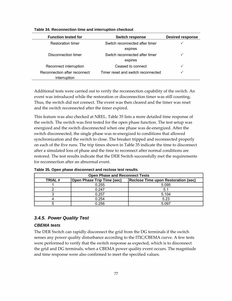
Table 34. Reconnection time and interruption checkout
Function tested for Switch response Desired response Restoration timer Switch reconnected after timer
expires
Disconnection timer Switch reconnected after timer expires
Reconnect interruption Ceased to connect Reconnection after reconnect
interruption Timer reset and switch reconnected
Additional tests were carried out to verify the reconnection capability of the switch. An event was introduced while the restoration or disconnection timer was still counting. Thus, the switch did not connect. The event was then cleared and the timer was reset and the switch reconnected after the timer expired.
This feature was also checked at NREL. Table 35 lists a more detailed time response of the switch. The switch was first tested for the open phase function. The test setup was energized and the switch disconnected when one phase was de‐energized. After the switch disconnected, the single phase was re‐energized to conditions that allowed synchronization and the switch to close. The breaker tripped and reconnected properly on each of the five runs. The trip times shown in Table 35 indicate the time to disconnect after a simulated loss of phase and the time to reconnect after normal conditions are restored. The test results indicate that the DER Switch successfully met the requirements for reconnection after an abnormal event.
Table 35. Open phase disconnect and reclose test results
TRIAL # Open Phase Trip Time (sec) Reclose Time upon Restoration (sec)Open Phase and Reconnect Tests
1 0.255 5.0952 0.247 5.13 0.257 5.1044 0.254 5.235 0.256 5.097
3.4.5. Power Quality Test CBEMA tests The DER Switch can rapidly disconnect the grid from the DG terminals if the switch senses any power quality disturbance according to the ITIC/CBEMA curve. A few tests were performed to verify that the switch response as expected, which is to disconnect the grid and DG terminals, when a CBEMA power quality event occurs. The magnitude and time response were also confirmed to meet the specified values.
77

The power quality function in the switch controller is represented by five magnitude and time response settings that can be adjusted by the user via the Engineering HMI. These settings are shown in colored lines in Figure 29; the corresponding setting labels are defined in the controller.
Details on Figure 29 (b)
(a)
CBEMA Curve
0
20
40
60
80
100
120
140
160
180
200
0.01 0.1 1 10 100
Time (s)
Perc
ent N
omin
al V
olta
ge (V
)
CBEMA Voltage #1
CBEMA Voltage #2
CBEMA Voltage #3
CBEMA Voltage #4
CBEMA Voltage #5
78

(b)
79
Figure 29. CBEMA curve specification ned in controller simplified method was carried out to test the CBEMA settings. Actual values that
ied
defi
Aapproximate the CBEMA curve were tested at NREL, and results are illustrated in Figure 32. From the initial observation, the switch managed to respond to the specifinterruption voltage within the specified time setting. The time response, however, was limited by the CB disconnection timer. Results are listed in Table 36.
Figure 30. Response to CBEMA (CBEMA voltage #1)
able 36. Switch resp A curve
(%
tripc
T onse to interruption voltage according to ITIC-CBEM
Alarm namea Interruption Filter time Tripped?b Tvoltage
of nominal) constant
CBEMA voltage #1 0.01 ms √ 8.5 + 80 ms 90 CBEMA voltage #2 105 0.01 ms √ 40 + 80 ms
(see note) CBEMA voltage #3 90 0.2 s √ 0 .14 + 0.08 sCBEMA voltage #4 105 0.5 s √ 0.22 + 0.08 s CBEMA voltage #5 90 10 s √ 9 + 0.08 s
a Switch trol Requiremen ument for the finition of s
disconnected and the event was displayed on the Engineering
Refer updated DER Con t doc de the variouCBEMA voltage functions. b √ indicates that the DER switchHMI.
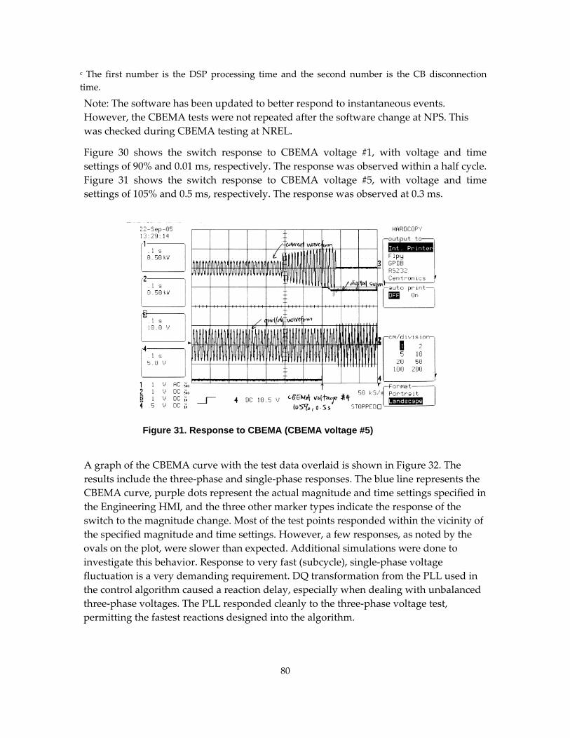
c The first number is the DSP processing time and the second number is the CB disconnection time. Note: The software has been updated to better respond to instantaneous events. However, the CBEMA tests were not repeated after the software change at NPS. This was checked during CBEMA testing at NREL.
Figure 30 shows the switch response to CBEMA voltage #1, with voltage and time settings of 90% and 0.01 ms, respectively. The response was observed within a half cycle. Figure 31 shows the switch response to CBEMA voltage #5, with voltage and time settings of 105% and 0.5 ms, respectively. The response was observed at 0.3 ms.
Figure 31. Response to CBEMA (CBEMA voltage #5)
A graph of the CBEMA curve with the test data overlaid is shown in Figure 32. The results include the three‐phase and single‐phase responses. The blue line represents the CBEMA curve, purple dots represent the actual magnitude and time settings specified in the Engineering HMI, and the three other marker types indicate the response of the switch to the magnitude change. Most of the test points responded within the vicinity of the specified magnitude and time settings. However, a few responses, as noted by the ovals on the plot, were slower than expected. Additional simulations were done to investigate this behavior. Response to very fast (subcycle), single‐phase voltage fluctuation is a very demanding requirement. DQ transformation from the PLL used in the control algorithm caused a reaction delay, especially when dealing with unbalanced three‐phase voltages. The PLL responded cleanly to the three‐phase voltage test, permitting the fastest reactions designed into the algorithm.
80

As previously observed, the breaker opening delay (a mechanical limitation) prevented the unit from optimally complying with the CBEMA curve. On average, the breaker would fully disconnect no faster than 90 ms after the most severe transients.
0
50
100
150
200
250
300
350
400
450
500
0.0001 0.001 0.01 0.1 1 10 100
Time (s)
Perc
ent N
omin
al V
olta
ge (V
)
CBEMA3-phase changeVa changeVb changeController Settings
Single-phase PLL response error
Figure 32. CBEMA curve test performed at NREL
The test result showed that a three‐phase response setting can be programmed to meet the CBEMA voltage curve characteristics. However, the same setting can be less sensitive for the single‐phase CBEMA event. Further study is suggested to obtain the high‐speed response required to meet the CBEMA on a single‐phase basis.
3.5. Test Summary This section provides the status of each test and issues encountered that still need to be improved for future certification. Table 37 is a summary of the DER Switch tests. If the test results had deviations on the order of 2.5%, a symbol is used to indicate highly satisfactory prototype tests. Test results with deviations on the order of 25% are indicated by the satisfactory ; test results with deviations greater than 25% are shown by the unsatisfactory . N/A indicates the information was not applicable for this test. Many prototype time responses were unsatisfactory, mainly because of compensation errors that can be easily corrected with some additional effort.
81

Table 37. DER Switch test status and summary
Tests Status Improvements for future certification
Relay function test: Detect / Trip
Magnitude response
Time response
Overvoltage (59)
Undervoltage (27)
• Voltage sensor calibration
• Incorporating switch opening delay in time setting
Overfrequency (81O)
Underfrequency (81U)
• Compensation for delay in PLL frequency measurements
• Incorporating switch opening delay in time setting
Phase sequence (46) tests
N/A N/A
Instantaneous (50)
Time overcurrent (51)
• Incorporating switch opening delay in time setting
Set and digital event trip test
N/A N/A
IEEE 1547 function test:
Overvoltage tests
Undervoltage tests
• Voltage sensor calibration
• Incorporating switch opening delay in time setting
Overfrequency tests
Underfrequency tests
• Compensation for delay in PLL frequency measurements
• Incorporating switch opening delay in time setting
Synchronization tests N/A • Voltage sensor calibration
Reverse power tests • Incorporating switch opening delay in time setting
Unintentional islanding tests
• Incorporating switch opening delay in time setting
Open phase tests N/A N/A
Reconnect following abnormal disconnect
N/A
82

83
Tests Status Improvements for future certification
Relay function test: Detect / Trip
Magnitude response
Time response
tests
Power quality test:
CBEMA tests
3 Phase
1 Phase
• Unbalanced and single-phase power quality measurement
• Incorporating switch opening delay in time setting
3.5.1. Improvements The tests carried out on the DER Switch at NPS and NREL were intended to verify that the results matched the design goals. Overall, testing at NPS and NREL went well. NPS was able to improve the performance of the switch based on the test results and feedback from both parties. It was also very helpful to obtain inputs from NREL, which has extensive experience testing interconnection systems and applications.
Two major lessons learned are the magnitude response that had some error, and trip time response that needs to include the typical switch opening delay.
The comparison between the NPS and NREL test results for IEEE 1547 voltage tests showed that the percent error of those results varied. NPS realizes that the tests performed at its test facility did not use the actual event level as specified by IEEE 1547; the tests performed at NREL reflect the actual event levels that may have larger delta deviations from nominal, and may have caused larger measurement errors. Also, a few points in the sensor‐controller chain can be looked at to fine tune the measurements and reduce these errors. The calibration settings used in the DER Switch reflect default levels in the switch controller. This calibration effort requires additional time invested up‐front, and a more detailed calibration process will be incorporated into the system’s commissioning in the future.
Additional thought should also be given to automatic calibration procedures for the DER Switch. Other sources of error are due to the fixed point arithmetic and the limited analog to digital signal resolution in the controller. Efforts to reduce errors can be explored in future projects. As for the trip time response, the concept of including the typical switch opening delay is not complicated. Detailed snaplogs will be taken in cases where errors were seen between the predicted and actual trip times in future tests and analyzed. NSP, however, did not tackle this task under this project since the code processor is running out of memory. Optimization of the controller code and elimination of some of the control aspects that are not deemed important will mitigate the limitation

84
of code memory. More considerations are required to properly address these concerns. Another feature that can be included to enhance this application is the SmartView HMI software. Its customizable user interface would make the DER Switch easier to use and control. The Engineering HMI that came with the package was very helpful, but it contains a lot of information that most users will not require. Incorporating SmartView support for the DER Switch product would be relatively simple and significantly enhance user friendliness.
In summary, the prototype DER Switch accomplished its most critical objectives and moves DER technology in the right direction. All the feedback obtained from the test results performed at NSP and NREL provided valuable information to improve the functionality of the DER switch. With the lessons learned from this prototype DER Switch, a next generation DER Switch with CB, SCR, or IGBT technology is possible.

85
86
4.0 Conclusions and Recommendations The DER Switch program surveyed a range of requirements for grid interconnecting DG equipment. This led to the design of a DG technology‐neutral grid interconnection device that is not integrated into the DER package. The resulting DER Switch design is technology neutral and can be used with inverter and machine DG units. The DER Switch can be used in a wide range of applications as described in section 2.1. The specification of the DER Switch was based on past NPS project experience. Such a switch is cost effective in low‐voltage applications at a current rating higher than 200 A. Preliminary designs were made for electromechanical and semiconductor‐based DER Switches. A semiconductor‐based switch costs more than an electromechanical one, but it makes it possible to meet requirements for fast disconnection and power quality requirements such as CBEMA. The prototype DER Switch was constructed with CB technology to keep the prototype cost low. A detailed test program at NPS and NREL has been completed to verify the protective relay functions and IEEE 1547 functions implemented in the switch controller. The test results indicate a successful system and control architecture for the DER Switch. Testing showed that stronger focus should be placed on calibration procedures and methods to improve measurement accuracy and tolerance levels for the DER Switch to meet utility‐grade relay standards. The DER Switch shows all the characteristics necessary to meet the IEEE 1547 standards and improved accuracy in measurements will help meet the target of a certifiable DER Switch. Further testing will enable detailed analysis of response of the switch to single‐phase events. This will also be used to resolve the differences between the NPS and NREL test results.
The complete control of the DER Switch is implemented in a single DSP package. The DSP activates switch operation, performs protective relaying functions, and is compatible with the SmartView HMI software for enterprise energy management. The integration of all these functions into a single DSP helps achieve the reduction in equipment target as set out in the program goals. The use of standard commercially available components for the design and use of components well within the ratings margin helps achieve the reliability goals for the switch. More detailed tests and analysis would be required to obtain the exact reliability characteristics of the DER Switch. The decoupling of the interconnection switch from the DG equipment allows for fast repair; the only limitation is that of spares availability. The ability to identify unintentional islanding situations quickly and reliably and to resynchronize was demonstrated during the test program. The present HMI implemented in the DER Switch is an engineering interface that provides full flexibility in making changes to settings. This also allows easy testing and data collection from the prototype DER Switch. Conversion of this Engineering HMI to the SmartView HMI will provide a complete enterprise energy management interface.
The main goal has been to design a flexible utility interconnection device for DG applications. Studies conducted during the DER Switch program indicate unique

87
advantages for a grid interconnection device that uses semiconductor‐based switches, especially for use in network grids. Such a high‐speed switch can also be used to meet higher power quality goals for loads connected to DG sources.
Further testing of the DER Switch can be used to verify the ability to detect and trip a wider range of grid events. Particular attention needs to be focused on refining the control algorithms used to meet the CBEMA curve requirements while minimizing nuisance trips.
The accuracy of the relay functions can be improved by using more detailed calibration processes to compensate for sensor errors. Additional thought should also be given to automatic calibration procedures for the DER Switch. A floating point DSP platform can help mitigate some of the loss of accuracy related to fixed‐point conversions. The floating point DSP platforms can be used to integrate more advanced control and protection algorithms. The mechanical layout of the switch should be optimized for building a more compact switch. Future versions of the DER Switch should also focus on cost reduction to make the technology competitive for a wider range of applications.

88
5.0 References [Peng] F.Z. Peng, “Special issues on distributed generation,” IEEE Transactions on Power Electronics, Vol. 19, No 5, pp. 1157−1158, Sept. 2004.
[SCC21] IEEE SCC21 Standards Coordinating Committee on Fuel Cells, Photovoltaics, Dispersed Generation, and Energy Storage ‐ http://grouper.ieee.org/groups/scc21/index.html.
[Smith] Smith, J.W.; Brooks, D.L., “Voltage impacts of distributed wind generation on rural distribution feeders,” Transmission and Distribution Conference and Exposition, 2001 IEEE/PES, pp. 492−497 vol. 1.
[CBEMA] CBEMA/ITIC ‐ www.itic.org/technical/iticurv.pdf.
[IEEE 1547] IEEE 1547 ‐ IEEE Standard for Interconnecting Distributed Resources with Electric Power Systems, June 2003.
American National Standards Institute (ANSI). (January 1993). IEEE Recommended Practices and Requirements for Harmonic Control in Electrical Power Systems. IEEE Std 519‐1992 (Revision of IEEE Std 519‐1981). New York, NY: Institute of Electrical and Electronics Engineers, Inc.
[UL1741] UL1741 ‐ Inverters, Converters, and Controllers for Use in Independent Power Systems, Underwriters Laboratories Inc., January 2001.
[UL508A] UL508A – Outline for investigation for Industrial control panels, Oct. 1993.
[ConEd] Con Edison, “Specification EO‐2115, Revision 6: Handbook of General Requirements for Electrical Service to Dispersed Generation Customers,” 2004.
[CERTS] R. Lasseter et al., The CERTS MicroGrid Concept, LBNL‐50829, April 2002.
[Northern Test Plan] Final In‐House Prototype Test Plan, Energy Commission Deliverable Number: D‐2.1.17, NREL Deliverable Number: D‐1.15, April 2005.

89

90
6.0 Glossary
Acronym Definition A/D analog to digital ASCB analog signal conditioning board BIL basic insulation level CB circuit breaker CT current transformer CBEMA Computer and Business Equipment Manufacturers’ Association DER Distributed Energy Resource DERTF Distributed Energy Resource Test Facility DG distributed generation/distributed generator DSP digital signal processor EMI electromagnetic interference EPS electric power system HMI human machine interface IEEE Institute of Electrical and Electronics Engineers IGBT integrated gate bipolar transistor IGCT integrated gate commutated thyristor ISR interrupt service routine ITIC Information Technology Industry Council MTTF mean time to failure MTTR mean time to repair Microgrid collection of DG aggregated and interconnected to the EPS NPS Northern Power Systems NREL National Renewable Energy Laboratory O&M operations and maintenance PIER Public Interest Energy Research (Program) PLL phase locked loop PT potential (voltage) transformer PWM pulse width modulation RTU remote terminal unit SCADA supervisory control and data acquisition SCR silicon-controlled rectifiier SmartView® NPS SCADA System UPS uninterrupted power supply X/R inductive impedance to resistance ratio
SmartView® is a trademark of Northern Power Systems.

91

Appendices
• Appendix A: Specification Summary of the DER Switch
• Appendix B: Prototype DER Switch Photos
• Appendix C: SmartView Documentation
• Appendix D: NREL Modeling and Simulation Report
• Appendix E: NREL’s Test Report
• Appendix F: Omicron Technical Data Sheets
• Appendix G: Omicron
These appendices are available in separate volumes, CEC‐500‐2006‐XXX‐APA–CEC‐500‐2006‐XXX‐APG.