
Fixing the Curtice Model
11
1 Fixing the Curtice FET Model Steve Maas Applied Wave Research 1960 E. Grand Ave., El Segundo, CA 90245, USA Phone & FAX: 310-726-3000 [email protected] Abstract Convergence difficulties are common in nonlinear analyses of circuits using a Curtice model. The problem is not the model itself, but limitations of the parameters describing the gate I/V characteristic. In this paper, we show why that failure occurs, and show how the model can be modified to prevent it. Introduction The venerable Curtice-Ettenberg FET model (traditionally called, simply, the Curtice model ) [1] has existed for almost two decades. During that time, it has been used extensively for all kinds of microwave circuit designs. It is as fundamental to GaAs MESFET circuit design as the Shichman and Hodges model has been for circuits using silicon FETs. The model, in one form or another, has been implemented in virtually all circuit simulators. Many have extended the model to include nonlinear capacitances and other effects that were not in the original publication. Still, there are perennial problems in using the model. Designers frequently encounter convergence difficulties and errors from incorrect transconductance, especially near pinch-off. Most of these problems can be eliminated surprisingly easily; in this paper, we describe some simple modifications that remove most of the problems. The Curtice Model Most simulators’ “Curtice” model is actually an extension of the model described in the original publication. Even so, the basic equations for the channel current—the part of the model most interesting to us—remains unchanged. As with most of the classical FET models, the Curtice model consists of an equivalent circuit for the device that includes linear elements, nonlinear capacitances, diodes, and a nonlinear current source representing the channel current. The linear elements model such things as contact resistances and some of the parasitic capacitances, while the diodes model the gate-to-channel junction. Figure 1 shows the
-
Upload
abhay-kulkarni -
Category
Documents
-
view
225 -
download
4
Transcript of Fixing the Curtice Model

1
Fixing the Curtice FET Model
Steve MaasApplied Wave Research
1960 E. Grand Ave., El Segundo, CA 90245, USAPhone & FAX: 310-726-3000
Abstract
Convergence difficulties are common in nonlinear analyses of circuits using a Curtice model.
The problem is not the model itself, but limitations of the parameters describing the gate I/V
characteristic. In this paper, we show why that failure occurs, and show how the model can be
modified to prevent it.
Introduction
The venerable Curtice-Ettenberg FET model (traditionally called, simply, the Curtice model)
[1] has existed for almost two decades. During that time, it has been used extensively for all
kinds of microwave circuit designs. It is as fundamental to GaAs MESFET circuit design as
the Shichman and Hodges model has been for circuits using silicon FETs. The model, in one
form or another, has been implemented in virtually all circuit simulators. Many have extended
the model to include nonlinear capacitances and other effects that were not in the original
publication.
Still, there are perennial problems in using the model. Designers frequently encounter
convergence difficulties and errors from incorrect transconductance, especially near
pinch-off. Most of these problems can be eliminated surprisingly easily; in this paper, we
describe some simple modifications that remove most of the problems.
The Curtice Model
Most simulators’ “Curtice” model is actually an extension of the model described in the
original publication. Even so, the basic equations for the channel current—the part of the
model most interesting to us—remains unchanged. As with most of the classical FET models,
the Curtice model consists of an equivalent circuit for the device that includes linear elements,
nonlinear capacitances, diodes, and a nonlinear current source representing the channel
current. The linear elements model such things as contact resistances and some of the parasitic
capacitances, while the diodes model the gate-to-channel junction. Figure 1 shows the

2
equivalent circuit.
The channel current (which we can loosely call the drain current) is given by the following
expression:
(1)
where
(2)
In the above expressions, Vgs and Vds are the internal gate and drain voltages (i.e., not
including voltage drops across the gate, drain, and source resistances). Vds0 is a particular
voltage, usually the one at which the An polynomial coefficients were determined; β is a
constant; and τ is the gate-to-drain time delay. Note that V1 = Vgs at DC when Vds = Vds0. The
remaining terms, γ and λ, are also constants.
If we ignore (2) for a moment (say, by assuming that β = 0), Eq. (1) can be put in the form
(3)
Id Vgs Vds,( ) A0 A1V1 A2V12 A3V1
3+ + +( ) γVds( )tanh 1 λVds+( )=
V1 Vgs t τ–( ) 1 β Vds0 Vds–( )+( )=
+
-Vgs
Cgs(Vgs, Vds)
Ri
Rs
Id(Vg,Vd)
Rds,fCgd(Vgs,Vds)
Cds
Ci
Rd Rg
+
Vds
-
DrainGate
Source
Figure 1. Equivalent circuit of a FET, used in the Curtice model.
Id fg Vgs( ) fd Vds( )⋅=
3
where
(4)
and
(5)
This is a convenient expression, as it allows us to separate the effects of the gate and drain I/V
characteristics and to determine them easily; fg(Vgs) can be found from a plot of Id at fixed Vds,
and fd(Vds) at fixed Vgs . We can also see, quite clearly, the effect of the two functions. fg(Vgs),
which we call the gate I/V characteristic, is simply a cubic polynomial, which should be easy
to fit to any smoothly varying set of measured data. fd(Vds), the drain I/V characteristic, is a
hyperbolic tangent function. This function is used simply because any FET’s drain I/V
characteristic looks like a hyperbolic tangent curve when Vds > 0. The remaining term,
1 + λ Vds, accounts for DC drain-to-source resistance.
Now, what about Eq. (2)? This expression simply offsets the gate voltage, at high drain
voltages, to account for the tendency of power FETs to conduct at gate voltages below
pinch-off. In [1], this is described as a shift in pinch-off voltage, but it could also be called a
kind of subthreshold conduction. The correction is necessary only in power devices; models
for small-signal FETs should have β = 0.
Other elements of the equivalent circuit are straightforward, and we can dispense with them
quickly. The drain, source, and gate resistances are well known parasitics. Cds, the
drain-to-source capacitance, is largely a capacitance between metallizations on the chip, as is
Cgd, the gate-to-drain capacitance. Cgd has a significant nonlinearity only near Vds = 0. Cgs,
the largest capacitance, is moderately nonlinear. It is often modeled as a conventional
Schottky-junction capacitance, although that approach is terribly accurate, especially near
pinch-off. Rds,f and Ci model the dramatic decrease in drain-to-source resistance at RF and
microwave frequencies, and the diodes model conduction of the gate-to-channel junction.
The Model’s Characteristics
Users of the Curtice model and, especially, those who create parameter sets for it, should be
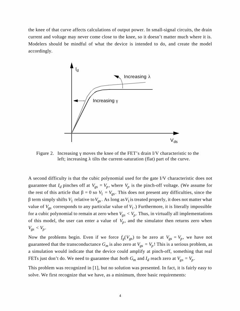
aware of some of its characteristics. First, there are only two parameters for adjusting the drain
I/V characteristic, λ and γ, and these have very different effects. As shown in Figure 2, λadjusts the slope of the curve, while γ adjusts the location of the knee. Clearly, one cannot
adjust, say, γ to match the knees of a set of drain I/V curves measured at several values of Vgs;
therefore, it is best to match the most important curve, and not worry about the rest. In a power
amplifier, the most important curve is the one representing the highest value of Vgs , because
fg Vgs( ) A0 A1V1 A2V12 A3V1
3+ + +=
fd Vds( ) γVds( )tanh 1 λVds+( )=
4
the knee of that curve affects calculations of output power. In small-signal circuits, the drain
current and voltage may never come close to the knee, so it doesn’t matter much where it is.
Modelers should be mindful of what the device is intended to do, and create the model
accordingly.
A second difficulty is that the cubic polynomial used for the gate I/V characteristic does not
guarantee that Id pinches off at Vgs = Vp , where Vp is the pinch-off voltage. (We assume for
the rest of this article that β = 0 so V1 = Vgs . This does not present any difficulties, since the
β term simply shifts V1 relative to Vgs . As long as V1 is treated properly, it does not matter what
value of Vgs corresponds to any particular value of V1 .) Furthermore, it is literally impossible
for a cubic polynomial to remain at zero when Vgs < Vp . Thus, in virtually all implementations
of this model, the user can enter a value of Vp , and the simulator then returns zero when
Vgs < Vp .
Now the problems begin. Even if we force fg(Vgs) to be zero at Vgs = Vp , we have not
guaranteed that the transconductance Gm is also zero at Vgs = Vp ! This is a serious problem, as
a simulation would indicate that the device could amplify at pinch-off, something that real
FETs just don’t do. We need to guarantee that both Gm and Id reach zero at Vgs = Vp .
This problem was recognized in [1], but no solution was presented. In fact, it is fairly easy to
solve. We first recognize that we have, as a minimum, three basic requirements:
Vds
IdIncreasing λ
Increasing γ
Figure 2. Increasing γ moves the knee of the FET’s drain I/V characteristic to the left; increasing λ tilts the current-saturation (flat) part of the curve.
5
1 Id = 0 at Vgs = Vp ;
2 Gm = 0 at Vgs = Vp ;
3 Id = Idss at Vgs = 0.
Imagine that we can factor (4), so it has the form
(6)
We must find the zeros and the term I0; once they are known, we can expand (6) to obtain the
An coefficients. The first of these requirements can be met by making one zero of the
polynomial, say, Vz3, equal to Vp, the pinch-off voltage. As it happens, making a second zero
equal to Vp satisfies the second requirement. Satisfying the third requires
(7)
where we have assumed that Vz2 = Vz3 =Vp and
(8)
This leaves us only one parameter, Vz1, to adjust the shape of the gate I/V characteristic to
match that of the measured data! Although we might conclude that it is difficult to obtain a
good “fit” to measured data with a Curtice model, it turns out that placing the remaining zero
at a large positive voltage (i.e., a few volts), it is usually easy to obtain good results.
Conversely, it makes it quite easy to fit a Curtice model using a simple spreadsheet or
MathCAD page1; no fancy numerical methods are needed.
Unfortunately, we’re not out of the woods yet. A set of model parameters determined in this
way might not work very well. To understand this, we must make a small digression into the
subject of nonlinear circuit analysis.
It is a distressing fact of life in the world of nonlinearity that it is rarely—almost never, in
fact—possible to solve nonlinear sets of equations directly. Invariably, some type of iterative
solution is necessary. To obtain any such solution, we must first estimate it, and then find some
way to improve the solution step by step, until we decide that it is good enough. For this
reason, solutions to sets of nonlinear equations are never perfect; they always come with some
amount of residual error. The trick is to make that error small enough to be negligible.
The key to solving such equations is to find a process that improves a given, inaccurate
solution. It does not have to solve it completely; as long as it can reliably improve an imperfect
1. See http://www.nonlintec.com/curtice.mcd to download an example.
fg Vgs( ) I0 Vgs Vz1–( ) Vgs Vz2–( ) Vgs Vz3–( )=
I0Idss
Vz1– Vp2
------------------=
Idss Idss fd Vd0( )⁄=
6
solution, we can start with a rough estimate of the solution, and apply the method to it
repeatedly until the problem is beaten into submission. One of the best techniques is Newton’s
Method, a process that involves using the derivatives of the equations to determine the manner
in which to modify the variables for which the equations must be solved.
In nonlinear circuit analysis, we use the derivatives of the FET’s I/V characteristic to estimate
new values of the drain and gate voltages. It should be no surprise that those derivatives must
be well behaved; if they have “kinks” in them or, heaven forbid, are discontinuous, the
estimate of the new solution may be very different on the two sides of the kink. If we are
unlucky, and the solution process traverses the kink as it modifies the voltages, the estimated
solution changes suddenly, and the simulator can lose convergence. This is true of both
harmonic-balance analysis and transient (SPICE) analysis.
By using a polynomial to describe the gate I/V characteristic, and setting it to zero below Vp,
we have created a huge kink in the transconductance—the derivative of Id with respect to
Vgs—at Vgs = Vp . Satisfying the three conditions above are not enough; we must satisfy a
fourth, namely dGm/dVgs = 0 at Vgs = Vp . This extra condition would use up our remaining
zero, leaving nothing to adjust for fitting the measured I/V characteristic to the model. This
just won’t do.
(In fact, we may have overstated the case a bit. The Curtice model usually works surprisingly
well in spite of this flaw, and as long as the model parameters are well chosen, convergence
failure at reasonable power levels is unlikely. Still, by fixing this problem, the model can be
made significantly more robust, so convergence occurs reliably even at high power levels.)
Fixing the Model
From this discussion, it appears that we need a couple of specific things:
1 The earlier requirements at Vgs = Vp and Vgs = 0 must be satisfied;
2 The additional requirement that dGm/dVgs = 0 at Vgs = Vp must be met;
3 More parameters must be freed, to provide more degrees of freedom for fitting the
model to measured I/V data.
These requirements have subtle implications. Specifically, the second implies that the FET
must have a “soft” pinch-off characteristic; that is, Id decays gradually around Vgs = Vp , and
the abrupt pinch-off of the classical model cannot exist. That’s actually good, because FETs
pinch off gradually, not abruptly. A model that meets these new requirements therefore is
likely to describe the FET better near pinch-off.
One way to meet some of these requirements is to limit Vgs to Vgs > Vp in some numerically

7
acceptable way, before using it in (1) and (2). Clearly, we cannot simply define a new Vgs
variable, say Vgs,x and say
(9)
because that would reintroduce the kink in Gm. A better solution is to use a function of the
form
(10)
This function limits Vgs,x to a maximum value of Vp, while creating a gradual transition near
Vp. The transition is controlled by δ; a large δ provides a more gradual transition, while δ = 0
creates an abrupt one, equivalent to (9).
With this change, Id trails off gradually its values at Vp, even as Vgs drops below Vp, and Gm
drops to zero. It does not, however guarantee Id to be zero below pinch-off. In fact, this change
alone can make matters worse: if the model parameters have not been extracted to ensure that
Id = 0 at Vgs = Vp , the FET may show substantial, even negative, current at pinch-off. We need
to make certain that the latter condition is also satisfied.
There are two ways to implement this second part of the solution. The first is simply to modify
the gate I/V characteristic in some way so that the Id = 0 condition at Vgs = Vp is met. This
approach probably requires the creation of a new expression for the gate I/V characteristic,
making users’ existing Curtice model libraries obsolete. Recognizing that this solution will
not endear the authors with circuit designers, we may consider a second approach: modify the
existing parameter set in a minimal manner, so that it satisfies these obviously necessary
requirements but does not change the I/V characteristic more than necessary. We should do
this in a way that does not modify the parameters if they already meet the pinch-off conditions.
We begin by assuming that the gate I/V characteristic simply fails to provide zero current when
Vgs = Vp , but it is otherwise well conceived. This condition is shown in Figure 3. Of course,
many other errors are possible, many of which are frightening. For example, it is possible for
fg(Vgs ) to have a minimum between Vp and Vgs = 0, so it is actually decreasing at pinch-off as
Vgs increases. We will not attempt to fix all such errors; at some point, the user has to take
responsibility for creating a model that is at least a reasonable representation of the device.
After some experimentation, we have determined that a simple and effective way to correct a
problem like the one shown in Figure 3 is simply to distribute the error linearly across the
range Vgs = (Vp , Vmax ), where Vmax is some maximum gate voltage. In many cases, Vmax = 0
Vgs x,
Vgs Vgs Vp>
Vp Vgs Vp≤
=
Vgs x, Vp 0.5 Vgs Vp– Vgs Vp–( )2 δ++( )+=

8
is the best value to use, as it preserves the Idss of the model. However, this value may not be
practical in devices having low pinch-off voltages. In such devices, a Vmax value of a few
tenths of a volt may be preferable.
The gate I/V characteristic is modified as
(11)
where V1 (which we have been assuming to be equal to Vgs) is as used in (1) and ∆Id is the
error in Id at Vgs = Vp . This change can be implemented simply by modifying the polynomial
coefficients:
(12)
The modification also works when ∆Id < 0. Additionally, we have found that it provides relief
in many situations that are even uglier than the one shown in Figure 3. Note that the
coefficients are not modified if they satisfy pinch-off conditions as provided.
Figure 3. An example of a poorly conceived model. The drain current does not reach zero at pinch-off, and the transconductance has a strong discon-tinuity at that point. A simple circuit using this FET model would not converge to a solution in harmonic-balance analysis. (A0 = 0.022, A1 = 0.046, A2 = -0.037, A3 = 0.030, and Vp = -0.6V.)
fg V1( ) fg V1( )Vmax V1–
Vmax Vp–------------------------∆Id–→
A0 A0 ∆Id
Vmax
Vmax Vp–------------------------–→
A1 A1∆Id
Vmax Vp–------------------------–→

9
These two modifications guarantee that at least two of the polynomial coefficients in (4) can
be determined independently, while retaining proper pinch-off characteristics and Idss. The
other two coefficients cannot be treated independently, as they are constrained by (12), but the
user still has somewhat more freedom than before in selecting those coefficients. If the fg(Vgs )
polynomial is well determined, although perhaps without satisfying the pinch-off conditions,
these operations force fg(Vgs) to satisfy them with minimal modification.
Example
The above modification has been included in the Curtice model used in Microwave Office, ver.
5.0 [2]. These modifications could be included in any other circuit simulator that provides a
capability for users to write their own models.
In the Microwave Office implementation, Vmax is normally zero, but is modified so that
Vmax - Vp > 0.5V in all cases. Vmax is not a user-modifiable parameter; that would make it
vulnerable to the same kind of misuse that gives rise to the errors it is designed to correct.
Similarly, δ is set to . This gives a smooth curve at pinch-off, without making the
gate I/V characteristic too soft.
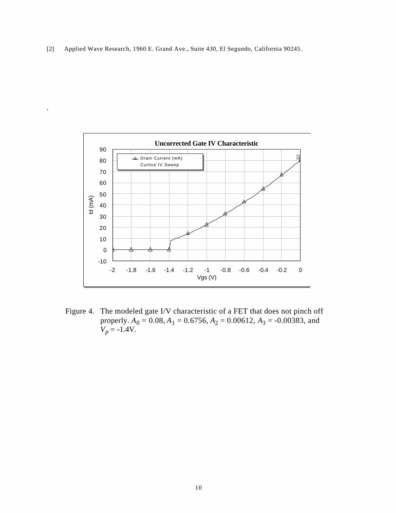
Figure 4 shows the gate I/V characteristic of a conventional Curtice model that does not pinch
off properly at Vgs = Vp . The current clearly does not reach zero at Vgs = Vp , and a little mental
differentiation shows that the transconductance also is nonzero at pinch-off. In fact, both are
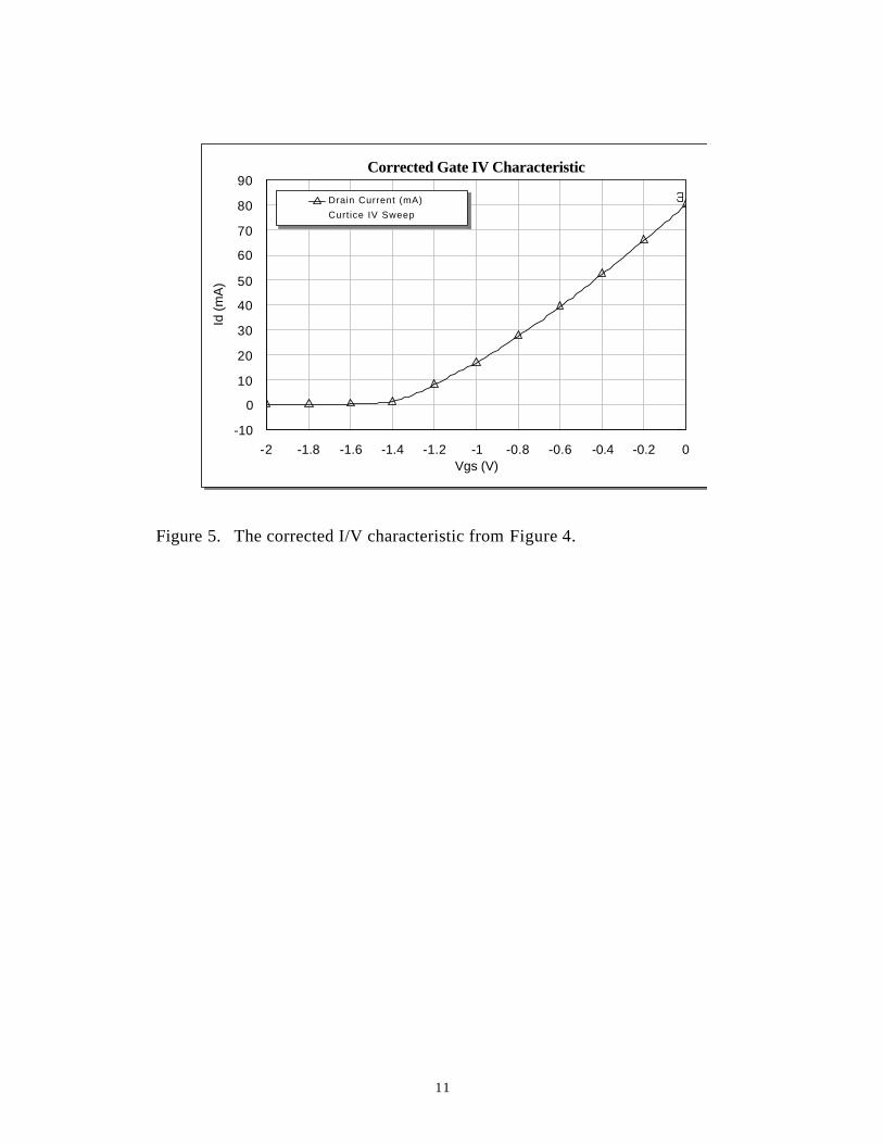
discontinuous. Figure 5 shows the same set of parameters with the above modifications. It is
clear that both the current and transconductance are now well-behaved near pinch-off, and the
characteristic has been modified minimally. The drain-current error of 10 mA at the pinch-off
voltage of -1.4V has been corrected, and the change in drain current is only about 3 mA above
-1V. The value of Idss, 80 mA, is preserved in the corrected characteristic.
Conclusions
The venerable Curtice model can have convergence difficulties when parameter extraction is
imperfect. In the classical model, the user is forced to choose between a parameter set that
matches the entire range of the measured I/V characteristics, or one that operates properly at
pinch-off. We can correct the model, however, by (1) limiting the value of Vgs in a numerically
acceptable manner, and (2) a modifying the A0 and A1 polynomial coefficients in a way that
minimizes changes in the I/V characteristic. Increased accuracy and robustness result.
References[1] W. R. Curtice and M. Ettenberg, “A Nonlinear GaAs FET Model for Use in the Design of Output Circuits
for Power Amplifiers” IEEE Trans. Microwave Theory Tech. , Vol. MTT-33, 1985, p. 1383.
2.5 10 3–⋅ Vp2
10
[2] Applied Wave Research, 1960 E. Grand Ave., Suite 430, El Segundo, California 90245.
.
-2 -1.8 -1.6 -1.4 -1.2 -1 -0.8 -0.6 -0.4 -0.2 0Vgs (V)
Uncorrected Gate IV Characteristic
-10
0
10
20
30
40
50
60
70
80
90
Id (
mA
)
Drain Current (mA)
Curtice IV Sweep
Figure 4. The modeled gate I/V characteristic of a FET that does not pinch off properly. A0 = 0.08, A1 = 0.6756, A2 = 0.00612, A3 = -0.00383, and Vp = -1.4V.
11
-2 -1.8 -1.6 -1.4 -1.2 -1 -0.8 -0.6 -0.4 -0.2 0Vgs (V)
Corrected Gate IV Characteristic
-10
0
10
20
30
40
50
60
70
80
90
Id (
mA
)
Drain Current (mA)
Curtice IV Sweep
Figure 5. The corrected I/V characteristic from Figure 4.