FIRST AMENDED COMPLAINT FOR PATENT INFRINGEMENT …
76
IN THE UNITED STATES DISTRICT COURT FOR THE DISTRICT OF DELAWARE S3 GRAPHICS Co., Ltd., a Cayman Islands Corporation Plaintiff, v. APPLE INC., a California Corporation, Defendant. C.A. No.: 11-862-SD DEMAND FOR JURY TRIAL FIRST AMENDED COMPLAINT FOR PATENT INFRINGEMENT Plaintiff S3 Graphics Co., Ltd. (“S3G”), for its First Amended Complaint against Defendant, Apple Inc. (“Apple”), hereby alleges as follows: NATURE OF THE ACTION 1. This is a civil action under the laws of the United States relating to patents and the protection of patent rights, e.g., 35 U.S.C. § 271 et seq., alleging infringement by Apple of four United States patents: U.S. Patent Nos. 5,945,997, 5,581,279, 6,353,440, and 5,977,960. PARTIES 2. S3G is a corporation organized and existing under the laws of the Cayman Islands, with its principal place of business at 2 nd Fl., Zephyr House, Mary St., P.O. Box 709, Grand Cayman, Grand Cayman Islands, British West Indies. S3G provides innovative graphics visualization technologies and GPU (graphics processing unit) products for mobile devices, desktop computers, and embedded systems. Case 1:11-cv-00862-SD Document 5 Filed 10/13/11 Page 1 of 11 PageID #: 53
Transcript of FIRST AMENDED COMPLAINT FOR PATENT INFRINGEMENT …

IN THE UNITED STATES DISTRICT COURT FOR THE DISTRICT OF DELAWARE
S3 GRAPHICS Co., Ltd., a Cayman Islands Corporation Plaintiff, v. APPLE INC., a California Corporation, Defendant.
C.A. No.: 11-862-SD
DEMAND FOR JURY TRIAL
FIRST AMENDED COMPLAINT FOR PATENT INFRINGEMENT
Plaintiff S3 Graphics Co., Ltd. (“S3G”), for its First Amended Complaint against
Defendant, Apple Inc. (“Apple”), hereby alleges as follows:
NATURE OF THE ACTION
1. This is a civil action under the laws of the United States relating to patents and the
protection of patent rights, e.g., 35 U.S.C. § 271 et seq., alleging infringement by Apple of four
United States patents: U.S. Patent Nos. 5,945,997, 5,581,279, 6,353,440, and 5,977,960.
PARTIES
2. S3G is a corporation organized and existing under the laws of the Cayman
Islands, with its principal place of business at 2nd Fl., Zephyr House, Mary St., P.O. Box 709,
Grand Cayman, Grand Cayman Islands, British West Indies. S3G provides innovative graphics
visualization technologies and GPU (graphics processing unit) products for mobile devices,
desktop computers, and embedded systems.
Case 1:11-cv-00862-SD Document 5 Filed 10/13/11 Page 1 of 11 PageID #: 53

2
3. Upon information and belief, Apple is a corporation organized and existing under
the laws of California, with its principal place of business at 1 Infinite Loop, Cupertino,
California 95014, which:
(a) engages in designing, developing, manufacturing, using, selling, and offering for
sale within the United States, and importing into the United States, certain electronic devices and
components including, for example and without limitation, the Apple iPhone, iPad, iPod Touch
mobile devices, Apple Mac desktop and notebook computers, and associated system and
application software sold or distributed by Apple (the “Accused Apple Products”); and
(b) provides certain related services for the Accused Apple Products, directly or
indirectly, within the United States.
SUBJECT MATTER JURISDICTION AND VENUE
4. This Court has subject matter jurisdiction over this action pursuant to 28 U.S.C.
§§ 1331 and 1338(a) because this civil action arises under the laws of the United States and
because this civil action arises under an Act of Congress relating to patents.
5. This Court has personal jurisdiction over Apple because Apple has established
minimum contacts with the State of Delaware. Apple, directly and/or through third-party
manufacturers, manufactures and/or assembles Accused Apple Products that are and have been
offered for sale, sold, purchased, and used within the State of Delaware. In addition, Apple,
directly and/or through its distribution networks, regularly places Accused Apple Products within
the stream of commerce, with the knowledge and/or understanding that the products will be sold
in the State of Delaware, and Apple provides related services to residents of the State of
Delaware. Thus, Apple has purposefully availed itself of the benefits of the State of Delaware,
both directly and indirectly.
Case 1:11-cv-00862-SD Document 5 Filed 10/13/11 Page 2 of 11 PageID #: 54
3
6. Apple transacts business in the State of Delaware because, among other things,
Apple manufactures and distributes, through its wholly owned Apple Store, Christiana Mall, 125
Christiana Mall, Newark, Delaware 19702, and through independent commercial retailers
located in the State of Delaware, Accused Apple Products that are offered for sale, sold,
purchased, and used within the State of Delaware, and has provided related services offered to
residents of the State of Delaware. Apple also has committed tortious acts of patent infringement
in the State of Delaware and is subject to personal jurisdiction in the State of Delaware. Venue
is thus proper in this judicial district pursuant to 28 U.S.C. §§ 1391(b), (c), (d), and 1400(b).
FACTUAL BACKGROUND
7. The technology at issue relates generally to hardware and software used in the
Accused Apple Products and related services.
8. The United States Patent and Trademark Office, having determined that the
requirements of law had been complied with, granted U.S. Patent No. 5,945,997 (“the ’997
patent”), entitled “BLOCK-AND BAND-ORIENTED TRAVERSAL IN THREE-
DIMENSIONAL TRIANGLE RENDERING,” on August 31, 1999. The ’997 patent issued
from application No. 08/883,536, filed on June 26, 1997. S3G owns by assignment the entire
right, title, and interest in and to the ’997 patent, including the right to bring this suit and to seek
injunctive relief as well as past, present, and future damages. A copy of the ‘997 patent is
attached as Exhibit 1.
9. The United States Patent and Trademark Office, having determined that the
requirements of law had been complied with, granted U.S. Patent No. 5,581,279 (“the ’279
patent”), entitled “VGA CONTROLLER CIRCUITRY,” on December 3, 1996. The ’279 patent
issued from application No. 08/147,456, filed on November 5, 1993, which is a continuation of
Case 1:11-cv-00862-SD Document 5 Filed 10/13/11 Page 3 of 11 PageID #: 55

4
application No. 07/811,944, now abandoned. S3G owns by assignment the entire right, title, and
interest in and to the ’279 patent, including the right to bring this suit and to seek injunctive relief
as well as past, present, and future damages. A copy of the ‘279 patent is attached as Exhibit 2.
10. The United States Patent and Trademark Office, having determined that the
requirements of law had been complied with, granted U.S. Patent No. 6,353,440 (“the ’440
patent”), entitled “HARDWARE ASSIST FOR YUV DATA FORMAT CONVERSION TO
SOFTWARE MPEG DECODER,” on March 5, 2002. The ’440 patent issued from application
No. 09/430370, filed on October 29, 1999, which is a continuation of application No.
08/619,203, filed on March 21, 1996, now U.S. Patent No. 6,005,546. S3G owns by assignment
the entire right, title, and interest in and to the ’440 patent, including the right to bring this suit
and to seek injunctive relief as well as past, present, and future damages. A copy of the ‘440
patent is attached as Exhibit 3.
11. The United States Patent and Trademark Office, having determined that the
requirements of law had been complied with, granted U.S. Patent No. 5,977,960 (“the ’960
patent”), entitled “APPARATUS, SYSTEMS AND METHODS FOR CONTROLLING DATA
OVERLAY IN MULTIMEDIA DATA PROCESSING AND DISPLAY SYSTEMS USING
MASK TECHNIQUES,” on November 2, 1999. The ’960 patent issued from application No.
08/707937, filed on September 10, 1996. S3G owns by assignment the entire right, title, and
interest in and to the ’960 patent, including the right to bring this suit and to seek injunctive relief
as well as past, present, and future damages. A copy of the ‘960 patent is attached as Exhibit 4.
12. Upon information and belief, Apple has infringed and continues to infringe,
directly and/or indirectly, one or more claims of each of the ’997, ’279, ‘440 and ’960 patents
Case 1:11-cv-00862-SD Document 5 Filed 10/13/11 Page 4 of 11 PageID #: 56
5
(collectively, “the Asserted Patents”), by engaging in acts that constitute infringement under 35
U.S.C. § 271, including, but not necessarily limited to:
(a) by making, using, selling, and/or offering for sale, in the State of Delaware
and elsewhere within the United States, and by importing into the State of Delaware and the
United States, certain electronic devices and components, including, for example and without
limitation, the Apple iPhone, iPad, an iPod Touch mobile devices, Apple Mac desktop and
notebook computers, alone or in combination with associated system and application software
sold or distributed by Apple;
(b) by providing one or more related services with respect to the foregoing
electronic devices and components, directly or indirectly, within the United States; and
(c) by inducing and/or contributing to acts of infringement by others with
respect to the foregoing electronic devices and components, with direct infringement being
accomplished, literally and/or under the doctrine of equivalents, by such persons when they use
at least one or more of such electronic products containing computing devices and/or related
software and/or services.
COUNT I — INFRINGEMENT OF U.S. PATENT NO. 5,945,997
13. Paragraphs 1-12 are incorporated by reference as if fully stated herein.
14. Apple has directly infringed and is directly infringing at least claims 1, 3-5, 9, and
16 of the ’997 patent, literally and/or under the doctrine of equivalents, by making, using, selling,
and offering for sale within the United States, and/or importing into the United States, one or
more of the Accused Apple Products and by providing related services that are covered by one or
more claims of the ’997 patent.
Case 1:11-cv-00862-SD Document 5 Filed 10/13/11 Page 5 of 11 PageID #: 57

6
15. Upon information and belief, Apple has indirectly infringed the ’997 patent by
contributing to and/or inducing, and will continue to contribute to and/or to induce, infringement
of at least claims 1, 3-5, 9, and 16 of the ’997 patent by others in this judicial district and
elsewhere in the United States, with direct infringement being accomplished, literally and/or
under the doctrine of equivalents, by users of at least one or more of the Accused Apple Products
and related services.
16. S3G has been and continues to be damaged by Apple’s infringement of the ’997
Patent, in an amount to be determined at trial. Upon information and belief, Apple has
knowledge of the ’997 patent and, if and to the extent it may be required, has received actual
notice of its infringement of the ’997 patent at least as of the filing date of the Complaint and/or
this First Amended Complaint, if not earlier.
17. S3G has suffered irreparable injury for which it has no adequate remedy at law
and will continue to suffer such irreparable injury unless Apple’s infringement of the ’997 patent
is enjoined by this Court.
18. Upon information and belief, Apple’s infringement of the ’997 patent is willful
and, together with other conduct, renders this case exceptional and entitles S3G to enhanced
damages under 35 U.S.C. § 284 and its reasonable attorney fees and costs incurred in prosecuting
this action under 35 U.S.C. § 285.
COUNT II — INFRINGEMENT OF U.S. PATENT NO. 5,581,279
19. Paragraphs 1-12 are incorporated by reference as if fully stated herein.
20. Apple has directly infringed and is directly infringing at least claims 1, 5, and 9 of
the ’279 patent, literally and/or under the doctrine of equivalents, by making, using, selling, and
Case 1:11-cv-00862-SD Document 5 Filed 10/13/11 Page 6 of 11 PageID #: 58

7
offering for sale within the United States, and/or importing into the United States, one or more of
the Accused Apple Products and by providing related services that are covered by one or more
claims of the ’279 patent.
21. Upon information and belief, Apple has indirectly infringed the ’279 patent by
contributing to and/or inducing, and will continue to contribute to and/or to induce, infringement
of at least claims 1, 5, and 9 of the ’279 patent by others in this judicial district and elsewhere in
the United States, with direct infringement being accomplished, literally and/or under the
doctrine of equivalents, by users of at least one or more of the Accused Apple Products and
related services.
22. S3G has been and continues to be damaged by Apple’s infringement of the ’279
Patent, in an amount to be determined at trial. Upon information and belief, Apple has
knowledge of the ’279 patent and, if and to the extent it may be required, has received actual
notice of its infringement of the ’279 patent at least as of the filing date of the Complaint and/or
this First Amended Complaint, if not earlier.
23. S3G has suffered irreparable injury for which it has no adequate remedy at law
and will continue to suffer such irreparable injury unless Apple’s infringement of the ’279 patent
is enjoined by this Court.
24. Upon information and belief, Apple’s infringement of the ’279 patent is willful
and, together with other conduct, renders this case exceptional and entitles S3G to enhanced
damages under 35 U.S.C. § 284 and its reasonable attorney fees and costs incurred in prosecuting
this action under 35 U.S.C. § 285.
Case 1:11-cv-00862-SD Document 5 Filed 10/13/11 Page 7 of 11 PageID #: 59
8
COUNT III — INFRINGEMENT OF U.S. PATENT NO. 6,353,440
25. Paragraphs 1-12 are incorporated by reference as if fully stated herein.
26. Apple has directly infringed and is directly infringing at least claims 1-4 and 12-
15 of the ’440 patent, literally and/or under the doctrine of equivalents, by making, using, selling,
and offering for sale within the United States, and/or importing into the United States, one or
more of the Accused Apple Products and by providing related services that are covered by one or
more claims of the ’440 patent.
27. Upon information and belief, Apple has indirectly infringed the ’440 patent by
contributing to and/or inducing, and will continue to contribute to and/or to induce, infringement
of at least claims 1-4 and 12-15 of the ’440 patent by others in this judicial district and elsewhere
in the United States, with direct infringement being accomplished, literally and/or under the
doctrine of equivalents, by users of at least one or more of the Accused Apple Products and
related services.
28. S3G has been and continues to be damaged by Apple’s infringement of the ’440
Patent, in an amount to be determined at trial. Upon information and belief, Apple has
knowledge of the ’440 patent and, if and to the extent it may be required, has received actual
notice of its infringement of the ’440 patent at least as of the filing date of the Complaint and/or
this First Amended Complaint, if not earlier.
29. S3G has suffered irreparable injury for which it has no adequate remedy at law
and will continue to suffer such irreparable injury unless Apple’s infringement of the ’440 patent
is enjoined by this Court.
Case 1:11-cv-00862-SD Document 5 Filed 10/13/11 Page 8 of 11 PageID #: 60

9
30. Upon information and belief, Apple’s infringement of the ’440 patent is willful
and, together with other conduct, renders this case exceptional and entitles S3G to enhanced
damages under 35 U.S.C. § 284 and its reasonable attorney fees and costs incurred in prosecuting
this action under 35 U.S.C. § 285.
COUNT IV — INFRINGEMENT OF U.S. PATENT NO. 5,977,960
31. Paragraphs 1-12 are incorporated by reference as if fully stated herein.
32. Apple has directly infringed and is directly infringing at least claims 1 and 7 of
the ’960 patent, literally and/or under the doctrine of equivalents, by making, using, selling, and
offering for sale within the United States, and/or importing into the United States, one or more of
the Accused Apple Products and by providing related services that are covered by one or more
claims of the ’960 patent.
33. Upon information and belief, Apple has indirectly infringed the ’960 patent by
contributing to and/or inducing, and will continue to contribute to and/or to induce, infringement
of at least claims 1 and 7 of the ’960 patent by others in this judicial district and elsewhere in the
United States, with direct infringement being accomplished, literally and/or under the doctrine of
equivalents, by users of at least one or more of the Accused Apple Products and related services.
34. S3G has been and continues to be damaged by Apple’s infringement of the ’960
Patent, in an amount to be determined at trial. Upon information and belief, Apple has
knowledge of the ’960 patent and, if and to the extent it may be required, has received actual
notice of its infringement of the ’960 patent at least as of the filing date of the Complaint and/or
this First Amended Complaint, if not earlier.
Case 1:11-cv-00862-SD Document 5 Filed 10/13/11 Page 9 of 11 PageID #: 61

10
35. S3G has suffered irreparable injury for which it has no adequate remedy at law
and will continue to suffer such irreparable injury unless Apple’s infringement of the ’960 patent
is enjoined by this Court.
36. Upon information and belief, Apple’s infringement of the ’960 patent is willful
and, together with other conduct, renders this case exceptional and entitles S3G to enhanced
damages under 35 U.S.C. § 284 and its reasonable attorney fees and costs incurred in prosecuting
this action under 35 U.S.C. § 285.
PRAYER FOR RELIEF
WHEREFORE, Plaintiff S3G prays the Court to issue the following judgment against
Apple:
A. That Apple has infringed, directly and/or indirectly, each and every one of the
Asserted Patents;
B. That Apple, its officers, agents, employees, and those persons in active concert or
participation with any of them, and their successors and assigns, be permanently enjoined from
direct and indirect infringement, including, but not limited to, inducement of infringement and
contributory infringement, of each and every one of the Asserted Patents, including, but not
limited to, an injunction against making, using, selling, and/or offering for sale within the United
States, and/or against importing into the United States, any products that infringe the Asserted
Patents and/or providing any services that infringe the Asserted Patents.
C. That S3G be awarded all damages adequate to compensate it for Apple’s
infringement of the Asserted Patents, such damages to be determined by a jury and, if necessary
Case 1:11-cv-00862-SD Document 5 Filed 10/13/11 Page 10 of 11 PageID #: 62

11
to adequately compensate S3G for the infringement, an accounting, together with prejudgment
and post-judgment interest at the maximum rate allowed by law;
D. That S3G be awarded enhanced damages, as provided in 35 U.S.C. § 284, up to
three times the amount found or assessed, for Apple’s willful infringement;
E. That the Court find this case to be exceptional, as provided in 35 U.S.C. § 285,
and award S3G its reasonable attorney fees, together with any and all allowable fees, costs,
and/other expenses incurred in connection with this action;
F. That the Court award such other relief as the Court may deem just and proper
under the circumstances.
DEMAND FOR JURY TRIAL
Plaintiff S3G demands a trial by jury on all claims.
Dated: October 13, 2011 Of Counsel: Thomas W. Winland Steven M. Anzalone Don O. Burley John R. Alison FINNEGAN, HENDERSON, FARABOW, GARRETT & DUNNER, LLP 901 New York Avenue, N.W. Washington, D.C. 20001 (202) 408-4000
YOUNG CONAWAY STARGATT & TAYLOR LLP
/s/ Karen L. Pascale ______________________________________ John W. Shaw (#3362) [[email protected]] Karen L. Pascale (#2903) [[email protected]] Karen E. Keller (#4489) [[email protected]] The Brandywine Building 1000 West Street, 17th Floor Wilmington, DE 19801 (302) 571-6600 Attorneys for Plaintiff, S3 Graphics Co., Ltd.
Case 1:11-cv-00862-SD Document 5 Filed 10/13/11 Page 11 of 11 PageID #: 63

EXHIBIT 1
Case 1:11-cv-00862-SD Document 5-1 Filed 10/13/11 Page 1 of 65 PageID #: 64

Case 1:11-cv-00862-SD Document 5-1 Filed 10/13/11 Page 2 of 65 PageID #: 65
United States Patent [19]
Zhao et ai.
[54] BLOCK- AND BAND-ORIENTED TRAVERSAL IN THREE-DIMENSIONAL TRIANGLE RENDERING
[75] Inventors: Randy X. Zhao, Fremont; Dong-Ying Kuo, Pleasanton, both of Calif.
[73] Assignee: S3 Incorporated, Santa Clara, Calif.
[21] Appl. No.: 08/883,536
[22] Filed: Jun. 26, 1997
[51] Int. CI.6 ........................................................ G06F 3/14
[52] U.S. CI. ............................................. 345/430; 345/429 [58] Field of Search ..................................... 345/418,419,
345/420, 429, 430, 431
[56] References Cited
U.S. PATENT DOCUMENTS
5,377,320 12/1994 Abi-Ezzi et al. ....................... 345/419
111111 1111111111111111111111111111111111111111111111111111111111111 US005945997 A
[11] Patent Number:
[45] Date of Patent:
5,945,997 Aug. 31,1999
5,574,836 11/1996 Broemmelsiek ........................ 345/427 5,801,714 9/1998 Holt ........................................ 345/420
Primary Examiner-Phu K. Nguyen Assistant Examiner-Cliff N. Vo Attorney, Agent, or Firm-Fenwick & West LLP
[57] ABSTRACT
A system and method for traversing and rendering a graphic primitive represented in screen space, employing block- and band-oriented traversal algorithms in texture mapping. Improved performance is achieved through burst-mode texture access and texture caching in connection with a texture map subdivided into squares. Block- and band-oriented traversal facilitates minimization of page breaks and texture cache swap-out. Improved determinism is facilitated by obviating the need for pixel sorting algorithms. Improved re-use of retrieved data segments in burst-mode access is facilitated.
21 Claims, 15 Drawing Sheets
1201
1208 Use
right-to-Ieft
N
Sort by y-coordinate, label vertices 0, 1, 2
N 1205 Use bottom-up
traversal
1207 Use top-down
traversal
y
y
1203 Use
left-to-right
N

Case 1:11-cv-00862-SD Document 5-1 Filed 10/13/11 Page 3 of 65 PageID #: 66
u.s. Patent Aug. 31,1999 Sheet 1 of 15 5,945,997
t (/)
N -,..... ~ ,.....
------< /'
C
" 0 ,..... ,..... -~--------------~
~~I

Case 1:11-cv-00862-SD Document 5-1 Filed 10/13/11 Page 4 of 65 PageID #: 67
u.s. Patent Aug. 31,1999 Sheet 2 of 15 5,945,997
y
~~
y
121 --------~~----------------- ~121
_____________________________ ~ 121
x
122
/120
/\ ~ /~ , \
/ \ / \
/ \ .......... \
.......... \ ~
122 x
..
FIG. 1A (PRIOR ART)
122
,
... --.
122 FIG. 18 (PRIOR ART)

Case 1:11-cv-00862-S
D D
ocument 5-1 F
iled 10/13/11 Page 5 of 65 P
ageID #: 68
d • rJl •
4 201 22 ~ ~
2 3 219 .....
2
104 ... 202 202 i
Y 20220;12011'" 1 _ __ v r 200 - 220 >
... 206 / I \ ~ ~
'""'" ~
~1 ~ ~ \C \C ...
(SCREEN SPACE) X FIG. 2A (TEXTURE SPACE) U FIG. 28 (PRIOR ART) (PRIOR ART) g2
~ ~ .....
y ~/ ~ o ....,
(SCREEN SPACE) X
MO '""'"
FIG. 2C (PRIOR ART)
Ul
Ul .... \C ""Ul .... \C \C ""-l

Case 1:11-cv-00862-SD Document 5-1 Filed 10/13/11 Page 6 of 65 PageID #: 69
u.s. Patent Aug. 31,1999 Sheet 4 of 15
301 Determine primitive
dimensions
302 Define edges
303 Define spans
304 First span
305 First pixel
306 Retrieve corresponding texel ..... -------.
308
Next pixel
y
FIGURE 3 (PRIOR ART)
5,945,997
310
Next span

Case 1:11-cv-00862-SD Document 5-1 Filed 10/13/11 Page 7 of 65 PageID #: 70
u.s. Patent Aug. 31,1999 Sheet 5 of 15 5,945,997
204
401 401 401 401
y 401 ~
I~ -401 401 - 2 00 -- 401
-= 401
401 :.....t 205 202··· 202 401 ~ 401
(SCREEN SPACE) x FIG. 4A
402
y
(SCREEN SPACE) x FIG. 48

Case 1:11-cv-00862-SD Document 5-1 Filed 10/13/11 Page 8 of 65 PageID #: 71
u.s. Patent Aug. 31,1999 Sheet 6 of 15 5,945,997
420
v
(TEXTURE SPACE) u FIG. 4C
405 405
! ! 8 pixels 8 pixels
40 403 403
Y
(SCREEN SPACE) x FIG. 4D

Case 1:11-cv-00862-SD Document 5-1 Filed 10/13/11 Page 9 of 65 PageID #: 72
u.s. Patent Aug. 31,1999 Sheet 7 of 15 5,945,997
503 d = 2
502 d = 1
256 texels
501 d = 0
512 texels
FIG. 5

Case 1:11-cv-00862-S
D D
ocument 5-1 F
iled 10/13/11 Page 10 of 65 P
ageID #: 73
601 601 601 601 601 v
601 601 601 601 601
601 601 601 601 601
601 601 601 601 601 ~
601 601 601 60( 601
" '-,..., -.l
(TEXTURE SPACE) u " 601
602 602 602 ... /
0 1 2 3
4 5 6 7
8 9 10 11
12 13 14 15 I
..... -
FIG. 6
¥' 802
_ .. _. r- 604
L..--_______ -------'~ 604
603 603 603 603
604
604
604
d • rJl • ~ ~ ..... ~ = .....
~ ~ ~
'""'" ~
'""'" \C \C \C
'JJ.
=~ ~ ..... 00 o ...., '""'" Ul
Ul .... \C ""-Ul .... \C \C ""-l

Case 1:11-cv-00862-SD Document 5-1 Filed 10/13/11 Page 11 of 65 PageID #: 74
u.s. Patent Aug. 31,1999 Sheet 9 of 15 5,945,997
§I
/ I } /1 I t:1 -, , !::< I ! H H' , -gl ~ , ~I ~ ~: 1
I
! \ £, - t"""1
~ HI
-~: ~ tt<1 ~: i ,
-tr -, - -, ,
h<' ~: I;:::' ::r: ~:
I~ H f-< I ~ ,..." I
: , ~ , :;;: ~: I - :
f-/-:< I I I -, , f-< : ..... ~i !
F.2T :-d. P- I.."i ~I I ,
§I
/ (
.- - -( - -0 0 0: 0 0 \0 \0 \0\ \0 \0
.- - f--~ I- - -0 0 ~~ I- 0 a \0 \0 - \0 \0
- - '-~ 1- - -0 0 l-S 1- a 0 \0 \0 l- I- \0 \0
- - I- H I- - -a a 1-~ I- a 0 \0 \0 I- I- \0 \0
.- - - - -0 a 0 0 0 \0 \0 \0 \0 \0
>

Case 1:11-cv-00862-S
D D
ocument 5-1 F
iled 10/13/11 Page 12 of 65 P
ageID #: 75
808
Span Walk Module .... ..
..
~
803 Texture Mapping ... _ ...
Engine
~ 802
Cache
~ 801
Texture Memory
800
\
809
Edge Walk Module ....
~ 807
Pixel Processing Module
~ 805
Frame Buffer Memory
~ 806
Display
FIGURE 8
810 .. Triangle Setup
d • rJl • ~ ~ ..... ~ = .....
~ ~ ~
!'"' '""'" \C \C \C
'JJ.
=~ ~ ..... '""'" c o ...., '""'" Ul
Ul .... \C ""Ul .... \C \C ""-l

Case 1:11-cv-00862-SD Document 5-1 Filed 10/13/11 Page 13 of 65 PageID #: 76
u.s. Patent Aug. 31,1999
,I
y
FIG. 9A x
101
,/
v
~902
FIG. 9C u
v
v 903
Sheet 11 of 15
FIG. 98
FIG. 9D
5,945,997
,/
u
101
,/
u

Case 1:11-cv-00862-S
D D
ocument 5-1 F
iled 10/13/11 Page 14 of 65 P
ageID #: 77
I I I I I I I I I I 1003 . 1004 1016 . 1016 1016 1016 . ...
~ ~
/ 1005 1006 1007 --,.. ~~H
v 021 ,;' ,
~ I ~ I V .,.. I " ,.1008 1009 1010
- 1022 _~~ ~H .
1
I ~ " '10~ 1023 " -10- ~ . ~ 1012 1013 -.- V ~ 1001
1024 ... 1tr-J,,~ 'I' ~~ .
1
1025 ~ ,
~I ~ I I(' -.,.. I i.'" }014 ... ~ _ 1002 ... 1016 . 1016 1026 'I' -~~~ . l- I--.
i027 ~ '" 1015 I I ,
1028 I I I I I I -'----------....\
(TEXTURE SPACE) FIG. 10 u 101
d • rJl • ~ ~ ..... ~ = .....
~ ~ ~
!"" '""'" \C \C \C
'JJ.
=~ ~ .... '""'" N o ...., '""'" Ul
Ul .... \C ""Ul .... \C \C ""-l

Case 1:11-cv-00862-S
D D
ocument 5-1 F
iled 10/13/11 Page 15 of 65 P
ageID #: 78
y I
y I I
x
122 1122 I··· 1
I ::::IIiiiiI1' \: I
(SCREEN SPACE)
FIG.11A x
122 1122 L··· 1
1 ............. 1 \ I
(SCREEN SPACE)
FIG.11C
y
1101
•
y I 1101
x
1122 1122 1 ... 1
I ~1101
(SCREEN SPACE)
FIG. 118 X
1122 1122 I··· I
I ~1101
(SCREEN SPACE)
FIG.11D
d • rJl • ~ ~ ..... ~ = .....
> = ~ ~
'""'" ~
'""'" \C \C \C
'JJ.
=-~ ~ ..... '""'" ~ 0 ...., '""'" Ul
Ul .... \C ""Ul .... \C \C -.....l

Case 1:11-cv-00862-SD Document 5-1 Filed 10/13/11 Page 16 of 65 PageID #: 79
u.s. Patent
1208 Use
right-to-Ieft
N
Aug. 31,1999 Sheet 14 of 15
1201 Sort by y-coordinate, label
vertices 0, I, 2
1205 Use bottom-up
traversal
1207 Use top-down
traversal
FIGURE 12
5,945,997
y
1203 Use
left-to-right
N

Case 1:11-cv-00862-S
D D
ocument 5-1 F
iled 10/13/11 Page 17 of 65 P
ageID #: 80
o 1 2 3 4 5 6 7 8 9 10 11 12 13 14 15 16 17 18 19 20 21 22 23 24 25 26 27
Y
0 1 2 3
/
v8 4 5
/ 2 3 /1 - --
UV11
FIG. 13
4
17 13 9 6
--
122
5 ( 6 7 I
59 / 58
26 27 / 24 25
121 22 23 18 19 20 14 15 16 10 11 12 _7 --
122
8 9 flO 11 12 13 14 15 16 17 / /
va /99 100 - -
92 93 94 95 96 97 98 - -/ 84 85 86 87 89 90 91 118 119 /
76 77 78 79 80 81 82 83 111 112 68 69 70 71 72 73 74 75 105 106 60 61 62 63 64 65 66 67 101 102 48 49 50 51 52 53 54 55 56 57 40 41 42 43 44 45 46 47 34 35 36 37 38 39 30 31 32 33 28 29
(SCREEN SPACE)
122
18 19 20 21 22 23 24
120 121 ~ 22 - I V1 I 113 114 115 116 117 --~
107 108 109 110 103 104
x
d • rJl • ~ ~ ..... ~ = .....
~ ~ ~
!'"' '""'" \C \C \C
'JJ.
=~ ~ ..... '""'" Ul o ...., '""'" Ul
Ul .... \C ""Ul .... \C \C ""-l

Case 1:11-cv-00862-SD Document 5-1 Filed 10/13/11 Page 18 of 65 PageID #: 81
5,945,997 1
BLOCK- AND BAND-ORIENTED TRAVERSAL IN THREE-DIMENSIONAL
TRIANGLE RENDERING
CROSS-REFERENCE TO RELATED APPLICATION
This application is related to U.S. patent application Ser. No. 081780,787 for "Pixel Reordering for Improved Texture Mapping", by Michael Cox, Dinyar Lahewala, and Don Kuo, filed Jan. 9, 1997, the disclosure of which is incorporated herein by reference.
BACKGROUND OF THE INVENTION
1. Field of the Invention
The present invention relates generally to texture mapping in graphics systems, and more particularly to a system and method of block- and band-oriented traversal to achieve improved bandwidth in such systems.
2. Description of Background Art
Texture mapping is the process of mapping an image onto
2 103 maps onto point Ast in the coordinates of surface 102 and to point Auv in texture map 101, or a group of points forming a region in texture map 101. Each of the mappings among display grid 103, surface 102, and texture map 101
5 may be point-to-point, point-to-region, region-to-point, or region-to-region. In conventional implementations of texture mapping systems, the mapping from display grid 103 to surface 104 and in turn to texture map 101 also generates a value d representing the level of detail for the particular
10 texel. Typically, d is a measure of the perceived distance of the point in the texture map, as determined by a z-value for the point in the frame buffer. Points that are perceived to be farther away have a lower level of detail representing decreased resolution. In retrieving texels from texture map
15 101, d is used to implement a multum in parvo map (MIP map) scheme wherein several texels may be averaged, or otherwise filtered, and mapped onto one pixel of the frame buffer. This filtering may be performed on-the-fiy, or filtered pixels may be pre-calculated at several selected resolution
20 levels and stored for later retrieval, resulting in improved performance. The higher the value of d, the lower the level of detail, and the more pixel-filtering is performed. In the limit, the entire texture map may theoretically be reduced to one pixel in the frame buffer.
a surface in a three-dimensional graphics system. This technique is well-known in the art, and is described, for example, in J. Foley et aI., Computer Graphics: Principles and Practice, 2d. ed., Addison-Wesley, 1990, at 741-44. 25
Conventional rasterization engines draw the image into the frame buffer by the known technique of scan conversion of primitives such as polygons and lines (see, for example, Foley et al.). Scan conversion takes as its input primitives defined in terms of vertices and orientations, and provides as
Referring now to FIG. 1, there is shown an example of texture mapping according to the prior art. The image to be mapped is referred to as a texture map 101, and its individual elements are referred to as texels. Texture map 101 is typically described in a rectangular coordinate scheme designated (u, v), and is ordinarily stored in some area of conventional memory, such as, for example, a conventional page-mode dynamic random-access memory (DRAM) or other paged memory. In the example of FIG. 1, four pages 110, 111, 112, 113 are shown, each corresponding to a portion of the image area containing a corresponding portion of texture map 101.
Surface 104 in three-dimensional space has its own coordinate system (s, t). In a typical three-dimensional graphics system, surface 104 may be a primitive such as a polygon; many such polygons may be defined in three-space to form a three-dimensional object or scene. Each such polygon would then have its own coordinate system (s, t) similar to the surface 104 indicated in FIG. 1. Based on the orientation of surface 104 in three-space, and on the position and orientation of the "camera", surface 104 is in turn mapped onto a two-dimensional display grid 103 stored in the frame buffer for display by the computer system. The mapping of surface 104 onto display grid 103 is accomplished by matrix transforms that are well-known in the art. Display grid 103 has coordinate system (x, y) and is typically implemented in an area of memory reserved for video display, such as video random-access memory (video RAM) e.g. VRAM or synchronous graphics random-access memory (SGRAM). Display grid 103 contains individual elements known as pixels, represented by distinct memory locations in video RAM.
Coordinates on display grid 103 are often considered to reside in "screen space". Similarly, coordinates in surface 102 are considered to reside in "surface space" and coordinates in texture map 101 are considered to reside in "texture space". The origins for each of the coordinate systems may be placed at any position, although typically the screenspace origin is placed either at bottom-left or top-right.
Each pixel in some region of display grid 103 maps onto a point on surface 104 and in turn to a point in texture map 101. Thus, in the example of FIG. 1, pointA"y of display grid
30 its output a series of pixels to be drawn on the screen. As each pixel is generated by scan conversion, a rasterization engine performs the necessary mapping calculations to determine which texel of texture map 101 corresponds to the pixel. The rasterization engine then issues whatever memory
35 references are required, such as texture fetch, z-fetch, z-writeback, color fetch, color write-back, and the like) to retrieve texel information for writing to the pixel being processed. Thus, memory references are issued in the order generated by the scan conversion. Conventionally, such
40 memory references are stored and managed according to a first-in first-out (FIFO) scheme using a FIFO queue.
It is known that conventional page-mode DRAM components incur access-time penalties when accessing memory locations from different memory pages. For example, in
45 some memory architectures such as SGRAM, an access to an open page requires one cycle, a read from a page not open requires nine cycles, a write to a page not open requires six cycles, and an access to an open page on a different bank requires three cycles. Thus, the above-described scheme of
50 issuing memory references in the order generated by scan conversion may incur such penalties, as the referenced areas of texture map 101 may lie in different pages. In fact, depending on the distortion of the texture boundaries resulting from the particular mapping transformation being
55 employed, references generated in scan conversion order may require repeated page-switching back and forth, also known as "thrashing". Since memory bandwidth is generally the bottleneck in fast generation of three-dimensional images, such repeated page-swapping results in diminished
60 performance. In addition, many memory systems employ a burst-mode
access scheme wherein a shared memory resource is made available for a particular period of time to one process, and is then unavailable to that process while it services other
65 processes. In order to maximize data transfer, it is advantageous to avoid page breaks within a burst. In essence, once a process has access to the shared memory resource, it is

Case 1:11-cv-00862-SD Document 5-1 Filed 10/13/11 Page 19 of 65 PageID #: 82
5,945,997 3
efficient for the process to retain access until the desired data segment has been transferred; page breaks may cause access to be shifted to another process, thus diminishing performance further.
Tiling has been found to be useful in improving data 5
transfer in burst-mode access and in reduce page breaks. Referring again to FIG. 1, texture space 101 is shown divided into four areas 110, 111, 112, 113 corresponding to pages in memory. This is an example of a typical tiling scheme wherein each area (or tile) is stored in a page of 10
memory, so that any scanning done within a tile does not cause page breaks. In general, page breaks only occur when scanning of one tile is complete and scanning of another tile begins. Typically, the tiled storage scheme yields an improved traversal path which reduces page breaks as 15
compared with linear traversal. Tiles and associated pages may be of any size, such as for
example 32x32 pixels, for a total of 1024 pixels. With 16-bit pixels, this corresponds to a page size of 2 KB.
Referring now to FIGS. 1A and 1B, there is shown an 20
example of an advantage of a tiled addressing scheme. FIG. 1A shows primitive 120 represented in a linear addressing scheme. Depending on the width of the frame buffer and page size, each scan line 121 may be represented in memory on its own page. For example, with a frame buffer of width 25
1024 and height 768, if each pixel has a 16-bit width, a 2 KB page holds a single scan line. Thus, each line segment of primitive 120 would be stored on a different page, and up to eight page breaks would be required to render primitive 120.
By contrast, FIG. 1B shows primitive 120 represented in 30
a tiled addressing scheme. If the entire primitive fits within a single tile 122, no page breaks are required to render primitive 120. Even if primitive 120 spans a plurality of tiles, in general fewer page breaks will be required than with 35
the linear addressing scheme of FIG. 1A. The above-described tiled addressing scheme can be
applied to image storage, and may be extended to color buffers and/or z-buffers as well.
4 by the locality of the texel references. Poor locality may result in excessive swapping of texels into and out of the texture cache. Conventional scan-line oriented traversal algorithms can result in poor locality, in particular if the texture primitives are oddly shaped. For example, when triangles are used as texture primitives, as is conventional, a very long and narrow triangle may span sufficient length along an x- or y-axis that, by the time the end of a span has been reached, the beginning of the span is no longer cached in the texture cache. Thus, when traversal of the next span begins, the required texels are no longer cached and must be retrieved from main texture memory. In other words, texture cache swap-out based on locality can result in poor hit rate when rendering certain shapes (such as long, narrow triangles).
Texel reordering techniques may be used to improve locality. However, the effectiveness of this approach is limited by the size of the access buffer, and may still fail to solve the texture space locality problem in some situations where the graphics primitives are of irregular shape. Texel reordering may be enhanced and locality improved by traversing two or more scan lines as a group. This approach results in additional complexity, as scheduling issues arise in determining which scan line is to be processed next. Such enhanced texel reordering also requires extensive feedback from the sorting algorithm and may introduce significant hardware design issues resulting from latency and verification.
Though the above-described techniques may be effective in improving rendering efficiency somewhat, unnecessary page-switching still occurs. In particular, burst-mode access to texture space results in unnecessary page thrashing and limited re-use of cached areas due to poor locality of texel references.
Another problem arises when burst-mode access is employed to access texture storage. Burst-mode typically retrieves a data segment having fixed length corresponding to the width of the memory bus (e.g. 64 bits, or 128 bits).
Other techniques have also been attempted in the prior art to minimize page breaks. both for linear and tiled access schemes. One example is the use of specialized memory in place of conventional page-mode memory components. See, for example, H. Fuchs and 1. Poulton, "Pixel-Planes: A VLSI-Oriented Design for a Raster Graphics Engine," in VLSI Design vol. 2., no. 3, 1981; M. Deering et aI., "FBRAM: A New Form of Memory Optimized for 3D Graphics," in Computer Graphics, Proceedings of SIGGRAPH, 1995; A. Schilling et aI., "Texram: A Smart Memory for Texturing," in IEEE Computer Graphics and Applications, 1996. Such systems generally improve memory bandwidth by, for example, associating memory directly with processing on an application-specific integrated circuit (ASIC), or by associating logic with memory directly on a DRAM chip. See A. Schilling et al. However, such techniques require highly specialized components that are generally more expensive than conventional page-mode DRAM.
40 Thus, burst-mode access to texture space typically retrieves more data than is immediately needed. Conventional texture storage mechanisms do not adequately cache the unneeded data for later re-use. Thus, additional accesses to this data may be generated where improved locality would have
45 resulted in more effective caching and reuse of the previously retrieved data segment.
What is needed is a system of reducing memory bandwidth by minimizing page-switching in conventional pagemode memory, so as to improve performance of graphic
50 engines for a wide range of client algorithms without substantially increasing the number of components or the overall cost. Specifically, what is needed is a system of improving locality of texel references over existing edgewalking and span-walking traversal techniques, and an
55 improved burst-access scheme for texture space that yields improved re-use of retrieved data.
SUMMARY OF THE INVENTION
In accordance with the present invention, there is provided a system and method of block- and band-oriented traversal in rendering of triangle primitives in a threedimensional graphics system, in order to minimize pageswitching and improve performance of the graphic engine.
Another attempt to reduce memory bandwidth is described in K. Akeley, "RealityEngine Graphics," in Com- 60
puter Graphics Proceedings of SIGGRAPH, 1993. Akeley describes a system of extreme memory interleaving. This technique requires significantly more memory chips than do conventional memory systems, and consequently is more expensive.
The present invention utilizes a texture cache to improve 65 access bandwidth to the texture map. Maximized bandwidth
is achieved by using burst-mode access to high-speed cache memory in a scheme providing improved re-use of
A texture cache may be used to improve access bandwidth to the texture map. However, texture cache hit rate is limited

Case 1:11-cv-00862-SD Document 5-1 Filed 10/13/11 Page 20 of 65 PageID #: 83
5,945,997 5
previously-retrieved data. The texture cache stores texels associated with a particular region for improved access. Locality in texture space is determined by the texture coordinate of each pixel. The texture cache is of finite size; therefore portions of the cache are swapped out when it 5
becomes less likely that they will be imminently accessed. Swap-out is performed according to locality. Thus, texture cache hit rate, which represents the rate at which texels may be accessed by referring to the texture cache, improves when locality of traversal is improved. The present invention is 10
directed toward improving locality of texel references so as to improve the texture cache hit rate, particularly in conjunction with burst-mode access.
Triangle rendering is accomplished by known techniques of edge walking and span walking. Each span of the triangle is determined, and then traversed. 15
In order to address the above-discussed problems, the present invention employs tiling, an improved texture storage scheme, and a modified traversal technique in order to improve texel reference locality and thereby increase hit 20
rate.
6 For a fixed dimension of eight pixels in screen space, the
maximum length of a texture space line segment is 1.41x 8=11.28, which rounds up to 12 texels. In some cases where fractional scaling components are resolved by truncation rather than rounding, as will be explained in more detail below a maximum texture space line segment may reach 16 pixels. A texture cache having dimensions of 12x12 (or, when truncation is being used, 16x16) texels will thus be guaranteed to be able to store the full width or height of a block or band subdivision of any primitive, so that traversal of the subdivided primitive will not require swap-out of the texture cache.
Given a fixed maximum dimension of any segment in texture space (12 texels, or 16 texels, in the example given above), a given number of texture cache squares must be available for contiguous access in order to guarantee memory locality. In a best-case situation where the orientation of the segment in texture space is either horizontal or vertical, the number of texture cache squares is determinable by dividing the maximum segment length in texture space by the dimension of the texture cache squares. Thus, in the above example, the 12-texel maximum segment length could be represented by three adjacent 4x4 texel squares if the segment were vertically or horizontally oriented. In a
Tiling improves locality of screen-space scanning, as described above. Typically, rendering of primitives in screen space requires fewer page breaks when a tiled addressing scheme is used.
The present invention further employs an improved texture storage scheme whereby texture space is divided into "squares" (which need not actually be squares, but may be rectangular or any other shape) of some fixed dimension, such as 4x4 texels. Each texture square is represented in a contiguous region of memory. Burst-mode access according
25 worst-case situation where the segment is oriented at 45 degrees in texture space, a worst-case situation requires a total of 13 squares of 4x4 dimension. Thus, if 13 texture cache squares are provided and available for contiguous access, memory locality is guaranteed for all line segments
30 for squares and bands of eight pixels in screen space.
to defined bit alignment and memory bus width results in retrieval of more data than is required to render the particular line segment being processed. The retrieved data segment is cached for later use. The improved texture storage scheme 35
provides for improved hit rate for the cached data segment
An additional advantage of the present invention using an eight-pixel wide block or band is that such divisions align naturally with page boundaries and thereby yield good locality in the z-buffer.
BRIEF DESCRIPTION OF THE DRAWINGS
FIG. I is a diagram showing texture mapping according to the prior art.
by taking advantage of the diagonal orientation of typical line segments in texture space. Specifically, texture squares serve to reduce page breaks when the texture cache is traversed.
Finally, the present invention employs a screen-space traversal scheme providing improved locality of texture accesses. The method of the present invention divides the image into a plurality of blocks or bands in screen space. Each block or band is of fixed width and height, such as for example 8x8 pixels or 16x16 pixels. An image primitive, such as a triangle, may span any number of blocks or bands
FIG. IAis a diagram showing a linear addressing scheme 40 according to the prior art.
FIG. IB is a diagram showing a tiled addressing scheme according to the prior art.
FIG. 2A is a diagram of a triangle primitive in screen 45 space according to the prior art.
in screen space. The portion of the primitive lying in any particular block or band can thus be expressed as a plurality of horizontal spans, each span having a maximum width 50
corresponding to the fixed width of the blocks or bands. Specific traversal paths are selected according to geometric characteristics of the primitives being rendered.
A MIP map texture mapping scheme employs an appropriate level of detail (LOD) determined based on available 55
texture space and dimension of the primitive segment being rendered. LOD therefore represents a scaling factor implemented by averaging or otherwise filtering pixel values for a set of pixels in screen space to derive a texel value for a single texel in texture space. Computation speed is improved 60
by restricting LOD scaling factors to powers of two, though this is not a requirement of the present invention.
Each span in screen space corresponds to a line segment in texture space. Given a MIP map texture mapping scheme, the length of the texture space line segment is determinis- 65
tic ally limited to be less than or equal to 1.41 w, where w is the fixed dimension of the blocks or bands in screen space.
FIG. 2B is a diagram of a texture image in texture space according to the prior art.
FIG. 2C is a diagram of a texture-mapped triangle primitive in screen space according to the prior art.
FIG. 3 is a flowchart of a method of edge- and spanwalking according to the prior art.
FIG. 4A is a diagram of a triangle primitive in screen space according to the present invention.
FIG. 4B is a diagram of a block in screen space for traversal according to the present invention.
FIG. 4C is a diagram of an area in texture space corresponding to the block of FIG. 4B.
FIG. 4D is a diagram of a band in screen space for traversal according to the present invention.
FIG. 5 is a diagram of an example of MIP map texture mapping according to an embodiment of the present invention.
FIG. 6 is a diagram of an implementation of a texture map with squares.
FIGS. 7 A and 7B are diagrams of a line segment in texture space.

Case 1:11-cv-00862-SD Document 5-1 Filed 10/13/11 Page 21 of 65 PageID #: 84
5,945,997 7
FIG. S is a block diagram of a system for practicing the present invention.
FIG. 9A is a diagram of a triangle primitive in screen space with a component line segment.
8 used. Referring also to FIG. 3, there is shown a flowchart of the process of edge- and span-walking. Once the screenspace primitive 200 has been defined 301, spans 202 of
FIG. 9B is a diagram of a line segment in texture space. 5
horizontal pixel rows in screen space are defined. Each span has a unique y-value representing the pixel row, or distance from the x-axis. Each span is demarcated by two edges of
FIG. 9C is a diagram illustrating burst-mode retrieval of a line segment in texture space using a linear addressing scheme.
FIG. 9D is a diagram illustrating burst-mode retrieval of a line segment in texture space subdivided into squares.
FIG. 10 is a detailed diagram showing an example of a line segment in texture space.
FIGS. lIA through lID are diagrams of traversal paths in screen space.
FIG. 12 is a flowchart of a method of selecting a traversal path.
FIG. 13 is a diagram of a traversal path in screen space, including pixel traversal order.
DETAILED DESCRIPTION OF IRE INVENTION
Referring now to FIG. S, there is shown a system SOO for practicing the present invention. Texture memory SOl contains a two-dimensional representation of a texture to be mapped onto primitives. Cache S02 provides temporary storage of portions of texture memory SOl for improved access speed, as will be described in more detail below. Graphic primitives are stored in a primitive storage portion
primitive 200, each of which may be defined by a linear equation. For example, in FIG. 2A, span 203 is defined by its y-value 206 representing the "height" or row-number of
10 the span. The demarcations of the span are defined by the linear equations describing edges 204 and 205 of primitive 200, which may in turn be derived from the three triangle points which define primitive 200. Thus, in order to define spans 202, edges are defined 302 based on the characteristics
15 of primitive 200, and spans 202 are defined 303 based on edges. Each span 202 contains a particular number of pixels, depending on the difference between the demarcating edge coordinates.
Primitive 200 is traversed span-by-span, and for each 20 span, the pixels within the span are processed in left-to-right
order. A first span 202 is selected 304, and a first pixel 305 within the selected span 202 is designated. Typically, the first pixel of the first span represents the leftmost pixel of the topmost span, though other span-walking and/or edge-
25 walking schemes may be used, as will be discussed in more detail below in connection with FIGS. lIA through lID.
Referring now also to FIG. 2B, a texel in texture map 219 corresponding to the selected pixel is then retrieved 306. MIP map texture mapping is used, as is known in the art, so
30 that a plurality of texture map 219 texels may be combined using averaging or some other filtering technique to generate a value for the selected pixels. In this manner, varying levels of detail are supported, so that for very small primitives 200, unnecessary retrieval of superfluous texel data is avoided. In
of memory (not shown), and define the size and shape of graphic elements, such as triangles or other polygons, to be displayed. Primitives are processed by triangle setup module S10 and traversed using edge walk module S09 and span walk module SOS to implement the scanning and traversal techniques described below. Texture mapping engine S03 performs the operation of mapping textures stored in texture memory SOl onto primitives. Pixel processing module S07 then performs z-buffering, texture lighting, fogging, alpha blending, and other pixel operations and writes the resulting 40
rendered image to frame buffer memory S05 or other video memory. The image in frame buffer memory S05 is sent to display S06. The present invention relates to the operation of texture mapping engine S03 and its relationships to the other components of FIG. S.
35 some embodiments, several versions of texture map image 220 may be stored, at varying levels of detail, so that no run-time computation need be done to generate filtered pixel values at a desired level of detail.
For illustrative purposes, in the present discussion of edge- and span-walking it is assumed that no texel filtering takes place. Thus, a single texel is retrieved and its data is rendered for the selected pixel in primitive 200. For example, pixel 201 of primitive 200 may correspond to texel 221 of texture image 220, so that texel 221 would be
45 retrieved and used in rendering pixel 201 in screen space. Other pixels of primitive 200 are processed similarly.
A check is performed 307 to determine whether the end of the current span has been reached. This check may be performed, for example, by comparing the x-coordinate of
50 the currently selected pixel with the demarcating edge 205 of primitive 200. If the end of the span has not yet been reached, span-walking continues by selecting 30S the next pixel in the span and repeating texel retrieval 306. In one embodiment, performance is improved by retrieving and
Referring now to FIG. 2A, there is shown a triangle primitive 200 in screen space to be rendered by accessing a texture map 219 in texture space. Primitive 200 typically represents some element of a graphic image on the display screen S06, and texture map 219 contains some graphic pattern or image 220 that is to be mapped onto primitive 200. Image 220 in texture map 219 may be distorted when mapped onto primitive 200 so as to give the impression of being viewed at an angle in three-dimensional space. For example, in a video game, primitive 200 may represent some portion of a spaceship flying through space, and texture map 219 may contain a graphic image of the markings and other surface features of the spaceship portion. In order to give the impression of three-dimensional action, the spaceship portion represented by primitive 200 may be elongated and 60
otherwise distorted so that it appears to be viewed from an angle in three-dimensional space. Texture image 220, when mapped onto primitive 200, is similarly elongated and distorted in order to preserve and enhance the impression. Edge- and Span-Walking
In order to map texture image 220 onto primitive 200, a technique known as edge- and span-walking is typically
55 processing each span via burst-mode access, rather than on a pixel-by-pixel basis. Burst-mode access will be discussed in more detail below in connection with FIGS. 9A through 9D.
Texel retrieval 306 for successive texels during spanwalking is facilitated by determining a texel walk vector in texture space corresponding to a single pixel movement in screen space. The texel walk vector represents a distance and direction of traversal in texture space that corresponding to a single pixel traversal in the x-direction in screen space. The
65 texel walk vector therefore depends on the relative sizes and orientations of the screen space primitive 200 and the texture map 220. In general, a relatively large primitive 200 such as

Case 1:11-cv-00862-SD Document 5-1 Filed 10/13/11 Page 22 of 65 PageID #: 85
5,945,997 9
that shown in FIG. 2A yields a relatively small texel walk vector, as a single pixel traversal in screen space represents less than a one texel traversal in texture space; therefore two or more successive pixels may map to the same texel in the texture image 220. Conversely, a relatively small primitive 5
200 yields a relatively large texel walk vector, as the texture map is scaled down and individual texels may be skipped.
10 As will apparent to those skilled in the art, alternative
embodiments employing other forms of subdivision, such as horizontal bands or variably shaped blocks, may be used without departing from the spirit or essential characteristics of the present invention.
When performing traversal by blocks or bands, the preferred embodiment selects among four different traversal paths. Referring now to FIGS. llA through lID, there are shown traversal paths 1101 for traversing tiles 122. FIG. llA shows a left-to-right, top down path; FIG. lIB shows right-to-Ieft, top-down; FIG. llC shows left-to-right, bottom up; and FIG. lID shows right-to-Ieft, bottom-up. Similar traversal paths may be applied to tiled sub-division as well. Traversal paths involving vertical scan lines rather than
Once the end of the span has been reached, a check is performed to determine 309 whether more spans 202 exist. This check may be performed, for example, by comparing 10
the y-value of the current span with the y-value characteristics of primitive 200. If additional spans exist, the next span is selected 310 and traversed as described above. If no additional spans exist, the primitive has been fully rendered and is ready for display. 15 horizontal scan lines may also be implemented.
Referring now also to FIG. 2C, there is shown an example of rendered primitive 240 having the same shape as primitive 200 but now containing a pattern generated by mapping texture map image 220 onto primitive 200.
The above-described method of span-walking generally 20
involves processing pixels sequentially, as the horizontal traversal accesses each pixel in order. Storage of pixel data in memory generally follows a left-to-right pattern, with adjacent pixels being stored in adjacent memory locations. Thus, horizontal traversal for span-walking is typically 25
implemented by accessing successive memory locations in screen memory 805. Memory locality is preserved during the span-walking process for individual spans, and page breaks are generally avoided so as to improve performance.
However, when the end of a span is reached and the next 30
span is to be processed, there may be a discontinuity in pixel data memory address retrieval. In other words, the memory location for the last pixel in a given span may not be adjacent to the memory location for the first pixel in the next span. When spans are sufficiently long, the jump from one span to 35
the next may cause a page break and thereby impair performance, as described above. Block- and Band-Oriented Traversal
Referring now to FIG. 12, there is shown a method for determining which traversal path to use, according to one embodiment of the present invention. A primitive such as a triangle having three vertices is assumed, each vertex having an x-coordinate and a y-coordinate in screen space. For purposes of this discussion, an origin (x,y=O,O) at the top left corner is assumed.
The three vertices are sorted 1201 by their y-coordinates, and labeled 0, 1, 2. Thus, vertex 1 has a y-coordinate between the y-coordinates for vertices 0 and 1. If vertex 1 lies to the right of the line segment connecting vertices 0 and 2 (step 1202), left-to-right traversal is selected 1203. Once this selection has been made, the x-coordinates of vertices 0 and 2 are compared 1204. If the x-coordinate of vertex 2 is less than the x-coordinate of vertex 0, bottom-up traversal is selected 1205. This is the traversal path shown in FIG. lIe. Otherwise, top-down traversal is selected 1207, which is the path shown in FIG. llA.
In 1202, if vertex 1 does not lie to the right of the line segment connecting vertices 0 and 2, right-to-Ieft traversal is selected 1208. Once this selection has been made, the x-coordinates of vertices 0 and 2 are compared 1209. If the x-coordinate of vertex 2 is less than the x-coordinate of
Referring now to FIG. 4A, there is shown primitive 200 in screen space, having similar dimensions and shape as shown previously in FIG. 2A. Blocks 401 having fixed xand y-dimensions are employed to subdivide the screen space and the primitive 200. In one embodiment, the dimensions of blocks 401 are eight pixels by eight pixels, although any suitable dimension may be used.
vertex 0, top-down traversal is selected 1207. This is the 40 traversal path shown in FIG. lIb. Otherwise, bottom-up
traversal is selected 1205, which is the path shown in FIG. lID.
The traversal paths shown in FIGS. llA to lID refer to blocks or bands. Within the blocks or bands, individual
45 pixels are traversed. In one embodiment, traversal of individual pixels is performed according to a path analogous to the block traversal path, though other paths may be used. Referring now to FIG. 13, there is shown an example of
Span-walking proceeds using a block-by-block traversal scheme so as to improve memory locality and reduce page breaks. Referring now to FIG. 4B, there is shown primitive 200 in screen space with block 402 being indicated for traversal. Block 402 is shown as being eight pixels wide by 50
eight pixels high, for illustrative purposes. Spans 403 are defined as described above, but with the additional delimiter of the block boundaries. The block boundary delimiter ensures that all spans have a maximum length corresponding to the block horizontal dimension. The dimension may be 55
chosen to be sufficiently small so as to avoid page breaks when jumping from one scan line to the next.
In an alternative embodiment, bands are used instead of blocks 401, the bands having fixed x-dimension or fixed y-dimension. Referring also to FIG. 4D, there is shown 60
primitive 200 in screen space, having similar dimensions and shape as shown previously in FIG. 2A. Here, bands 405
individual pixel traversal according to a left-to-right, bottom-up traversal path. Rendering order of individual pixels is indicated by numbers 1 through 117.
Referring again to FIG. 4B, block 402 contains a number of scan lines 403 limited by the vertical dimension of block 402. As stated previously, the width of each scan line is limited by the horizontal dimension of block 402. In the example shown, each of these dimensions is eight pixels. Referring also to FIG. 4C, there is shown texture map 219 containing texture image 220 as described above in connection with FIG. 2B. Texture space square 420 represents the region of texture image 220 corresponding to block 402 of FIG. 4B. Therefore, the texels contained in texture space square 420 will be sequentially accessed in the process of traversing block 402. If a texture cache 802 is being implemented, improved locality in texture space results in
are defined instead of blocks 401. Band boundaries serve as delimiters for span traversal and ensure a maximum span length corresponding to the band dimension. As with block dimensions, band dimensions may be selected to avoid page breaks when jumping from one scan line to the next.
65 improved performance in accessing individual texels. It is advantageous for the memory locations containing texel representations for texels in square 420 to be sufficiently

Case 1:11-cv-00862-SD Document 5-1 Filed 10/13/11 Page 23 of 65 PageID #: 86
5,945,997 11 12
The above-described MIP map scaling technique yields greater predictability in maximum span length in texture space. In general, a one-pixel walk in screen space corresponds to an L-pixel walk in texture space, where L is
proximate to one another so as to avoid page breaks in texture space memory accesses, and to maximize use of texture cache 802. In particular, burst-mode access to texture cache 802 is facilitated, given sufficient memory address locality and contiguity. As is known in the art, ~urst-n:ode access provides greatly improved performance III retneval operations. . .
In the preferred embodiment, square 402 dimensIO~ a~d texture cache size are selected with texture space localIty III mind so as to achieve the above goals. For example, for a square 402 dimension of eight pixels, the maximum span length in screen space is eight pixels. Since scaling may be used when performing texture mapping, an eight-pixel span may correspond to a span of any length in texture space, depending on the scaling factor. In order to remove the 15
uncertainty in maximum texture space span length, and also
5 dependent upon the level of detail (d) of the texture space representation to be used. Specifically, Land d are related by the expression
(Eq.3)
10 or, conversely,
in order to improve efficiency in texture map scaling, MIP map texture mapping is used. MIP Map Texture Mapping
Referring now to FIG. 5, there is shown an example of 20
MIP map texture mapping. Texture map 501 is shown having dimensions of 512 texels by 512 texels. A texture image is stored in texture map 501 at full size. Additional representations 502, 503 of the texture image are also shown, having successively lower levels of detail. Level of 25
detail, represented by a value d, represents a scaling factor to be used in texture mapping. For example, when the texture image is to be rendered on a relatively small primitive, such as one having a greater perceived distance, less detail is needed than when the texture image is to be 30
rendered on a larger primitive. Smaller representations 502, 503 are generated by averaging or otherwise filtering adjacent texels in full-size image 501. For example, a 256-texel square representation 502 is generated from full-size image 501 by filtering texel values for a 2x2 square to derive a texel 35
value for a single texel in the smaller representation. The filtering process is performed for successively larger sets of texels as the level of detail decreases (the 128-texel square filters 4x4 squares, etc.). In general, texel values for N texels in an MxM square are filtered (averaged) to generate one 40
pixel in a smaller representation, where:
M~(width of full size image )/(width of smaller image) (Eq.l)
and
(Eq.2) 45
(Eq.4)
In one embodiment, the texture map representation from the MIP map collection of representations is selected based on d. Referring again to FIG. 5, full-size representation 501 is designated as 0, representation 502 is designated as 1, representation 503 is designated as 2, and success~vely smaller representations are designated as successIvely higher values of d. Thus, if L is a power of two, d is. an integer value, and an appropriate texture map representatIOn can be selected having texel dimension equal to the pixel dimension in screen space.
For example, if L=4, an eight-pixel span in screen space corresponds to 32 texels of a full-size texture map representation, since 4x8=32. However, rather than using a full-size texture map representation, a scaled representation corresponding to the value of d=log2 4=2 will be used. Representation 2 has linear dimension one-quarter the size of the full-size representation. Thus, the eight-pixel screen space span corresponds to a texture space span of eight pixels. In general, with MIP map scaling and L having a value that is a power of two, the pixel dimension of the screen space span always equals the texel dimension of the corresponding texture space span.
If L is not restricted to values that are powers of two, d=log2 L may have a fractional component. d may then be represented as
(Eq.5)
where id is the integer component and fd is the fractional component. As discussed above texel map representations each have a designation corresponding to the value of d. In
In one embodiment, texels are filtered "on-the-fiy", as texels are retrieved for rendering. In another embodiment, texel filtering is performed in advance, and several representations at different sizes are stored. Several levels of detail are thus stored in a computation cache, containing the texture image at varying resolutions. Although this technique entails the use of additional storage space for a plurality of texel representations, it improves performance, since the calculation overhead of scaling "on-the-fiy" is avoided. Dimensions corresponding to powers of two are preferred for ease of calculation, however this is not required. A square texture image is shown for illustrative purposes, though other shapes such as triangles and rectangles may be used. In particular, a rectangular texture image may be used wherein the scaling factors along the u- 60
and v-axes are not equal, so that in effect a higher compression ratio is performed along one axis than along the other. This may be beneficial when, for example, the particular image demands additional resolution along a horizontal axis than along a vertical axis. However, in the following 65
discussion, uniform scaling factors along both axes are assumed.
one embodiment, if d is not an integer, the texel map representation having a designation closest to the value of d is chosen. Thus, if fd is less than 0.5 the texel map representation having designation of id is used, and if fd is greater than or equal to 0.5, the texel map representation having designation of id+1 is used. The texel map representation
50 most closely approximating the desired level of detail is thus chosen.
55
If fd is less than 0.5, and texel map representation id is used, the maximum dimension of a texture space span is given by:
(maximum screen space span)x2d/id (Eq.6)
which can be represented as:
(maximum screen space span)x2(id+!d)/2id (Eq.7)
and which reduces to:
(maximum screen space span)x2fd (Eq.8)
2fd has a maximum value of 2°.5=1.41, so that the maximum texture space span is no more than 1.41 times the maximum screen space span.

Case 1:11-cv-00862-SD Document 5-1 Filed 10/13/11 Page 24 of 65 PageID #: 87
5,945,997 13
If fd is greater than or equal to 0.5, and texel map representation id+ 1 is used, the maximum dimension of a texture space span is given by:
(maximum screen space span)x2d/id+l (Eq.9) 5
which can be represented as:
(maximum screen space span)x2(id+!d)/2id+ 1 (Eq.10)
and which reduces to:
(maximum screen space span)x2'"d-l (Eq.11)
14 Referring now to FIG. 6, there is shown an implementa
tion of texture map 101 with squares 601. Each square 601 contains a number of texels 602. For illustrative purposes, 16 texels are shown as constituting one square 601 in a 4x4 arrangement, though any number may be used. Texture cache 802 stores portions of texture map 101 on a square-by-square basis by providing a plurality of cache lines 604, each of which is capable of storing data describing one square 601. In the example shown, 16 bits 603 are shown in
10 each cache line 604, corresponding to the 16 texels 602 in a square 601. Texture cache 802 swap-out occurs on a square-by-square basis, so that an entire cache line 604 is replaced with new data when swap-out occurs.
2fd-1 has a minimum value of 2-0 .5=0.71, so that the maximum texture space span is no less than 0.71 times the 15
The implications of the subdivided texture map 101 implementation in the context of the present invention are as follows. Referring now to FIGS. 9A-9D, there is shown an example of the operation of the subdivided texture map 101 in conjunction with burst-mode access. FIG. 9A shows a simplified example of triangle primitive 120 in screen space
maximum screen space span. Given a MIP map scheme, texture space span is therefore
guaranteed to fall between O.71x(screen space span) and 1.41x(screen space span). With a fixed block width of eight pixels, and thus a maximum screen space span of eight pixels, the texture space span width will never exceed 1.41x8=11.28 texels. Rounding up, the texture space span width has a maximum dimension of 12 texels. Texture cache swap-out can thereby be avoided by providing for 12-texel span widths. In general, the MIP map scheme guarantees that no page breaks or swap-out will occur during traversal of any given block if texture cache 802 permits spans of 1.41 times the screen space block width.
20 103. A single horizontal line segment 901 is shown, as would be rendered in screen space in the course of drawing primitive 120.
Referring now to FIG. 9B, there is shown line segment 902 in texture space 101. Line segment 902 corresponds to
25 line segment 901, according to conventional texture mapping techniques as described above. As is typical in texturemapping operations, texture space line segment 902 is diagonal although the corresponding screen space line seg-
In an alternative embodiment, fractional components are truncated rather than rounded, so that 2fd has a maximum 30
value of 21.0 =2.00. In this case, the maximum texture space
span is no more than 2 times the maximum screen space span. Thus, an eight-pixel maximum length in screen space yields a maximum texellength of 16 texels.
ment 901 is horizontal. Referring now to FIG. 9C, there is shown an example of
burst-mode access to texture map 101 in the course of performing texture mapping operations. In order to access each texel in line segment 902, a number of successive texture space accesses need to be performed. With a defined
In either the rounded or truncated scheme, a discontinuity may be perceived when the value of d changes so that a different representation can be used. In some applications, such as video games where smooth movement is desired, the effect of the discontinuity can be jarring. Accordingly, in yet another embodiment, a tri-linear texture mapping scheme is employed, wherein both of the two nearest representations are averaged (or otherwise filtered) to generate a new representation more closely approximating the d value. Thus, for example, if d=2.9, representations for 2.0 and 3.0 are retrieved and combined using a filtering technique.
For example, four texels of each representation are averaged to generate two texel values, t2 .0 and t3 .0 . A new value is then generated from t2 .0 and t3 .0 using weighted averaging, so that:
or, more generally:
The tri-linear mapping scheme provides a more gradual shift from one MIP map representation to the next, and avoids the perceived discontinuity described above. Texture Map Squares; Burst-Mode Access
In one embodiment, texture map 101 is implemented according to an architecture wherein the map is subdivided into "squares" and texture cache 802 stores texture map 101 segments on a square-by-square basis. The term "square" is used to refer to texture map subdivisions in order to distinguish such subdivisions from tiles or blocks described previously. However, "squares" may actually be of any shape, in particular non-square rectangles.
35 fixed-width memory bus (e.g. 64 bits wide) using burstmode access, each such texture space access retrieves a texture-space line segment 903 corresponding to the defined width. Thus, in the example shown, each line segment 903 represents a byte-aligned, 64-bit contiguous area of texture
40 memory. Burst-mode access typically requires that all texture accesses occur in this manner, so that each access includes a portion of line segment 902 to be rendered, and an area of texture space 101 that is not of any immediate use. The unused portion of each retrieved line segment 903 can
45 be stored in a texture cache for later use. However, the hit rate for the texture cache is relatively low, since succeeding texture accesses typically involve adj acent rows rather than other portions of the same row. Thus, the row-based linear accessing scheme of FIG. 9C yields low hit rates for texture
50 caches, and most of the cached portions end up being discarded rather than reused. Successive accesses to a particular line segment 903 often occur far later, after the texture cache has been flushed, and therefore require reload-
55
ing without the benefit of the cache. Referring now to FIG. 9D, there is shown an example of
burst-mode access to texture map 101 with a subdivided texture map. Here, the addressing scheme for texture map 101 is based on "squares" 904 rather than horizontal rows of texels. For example, a 64-bit burst might provide a 4x4
60 square of texels rather than a 16-pixelline segment. Actual sizes of the squares in relation to the bus width depends on bit depth of the texels.
Each square 904 is stored in a cache line of texture cache 802 and is retrieved or discarded as is known for cache
65 storage. A burst-mode access to a particular portion of texture map 101 retrieves a square rather than a horizontal line segment. As can be seen in the example of FIG. 9D,

Case 1:11-cv-00862-SD Document 5-1 Filed 10/13/11 Page 25 of 65 PageID #: 88
5,945,997 15 16
The above examples are merely illustrative of sample embodiments. Other screen block sizes, texel square sizes, and cache line lengths could be used without departing from the essential characteristics of the present invention. In
unused portions of the retrieved burst are more efficiently re-utilized for successive portions of line segment 902. In general, since line segments in texture space 101 are typically diagonally oriented, successive portions of line segments often belong within the same square are previously cached portions, thus yielding better locality and hit rate than the linear addressing scheme exemplified in FIG. 9C.
In addition, the subdivided texture space scheme facilitates the use of fewer texture cache lines without sacrificing hit rate. Each texture cache line may be larger, since the square subdivision arrangement yields improved hit rates. The use of fewer cache lines improves performance by reducing the number of comparisons needed when maintaining the cache.
5 addition, in an alternative embodiment, a non-tiled texture map is used so that texture cache 802 operates on a texelby-texel, rather than on a square-by-square, basis, and the above-stated implementation details may be inapplicable.
Latency issues in connection with implementing the 10 present invention are dealt with in conventional manner
using a FIFO queue, as described in related application Ser. No. 081780,787. In one embodiment, texture cache 802 has sufficient FIFO depth to handle expected latency of operation.
To summarize, then, the subdivided texture space scheme of the present invention yields, for each burst access, a square (or other rectangular) region rather than a onedimensional line segment, thus providing improved texture hit rate and re-utilization, as well as facilitating the use of fewer cache lines.
As described previously, one embodiment of the present invention uses a MIP map texture mapping scheme which limits the length of texture space line segments to a maximum of 1.41 w, where w is the maximum length of line segments in screen space. This limitation, when combined
Referring now to FIG. 7A, there is shown an example of texture map 101 with squares 601 each containing 16 texels 15
in a 4x4 arrangement. As discussed above, an eight-pixel line segment in screen space corresponds to a maximum 12-texel texture space segment. Thus, in order to guarantee that no texture cache swap-out occurs, texture cache 802 is preferably of sufficient size to store a 12-texelline segment. 20
FIG. 7A shows a 12-texel line segment 701 oriented and situated so that the line segment is contained in three texel squares 601. Thus, in such a situation, three cache lines 604 are required to store all texels needed for mapping the 12-texel line segment.
In other situations, however, three cache lines 604 may not be sufficient for a 12-texel line segment. For example, referring now to FIG. 7B, line segment 702 is 12 texels in length, but is now oriented at a 45-degree angle, so that it spans 7 texel squares 601. Thus, in such a situation, 7 cache 30
lines 604 are required to store all texels needed for mapping the 12-texel line segment.
25 with the subdivided texture space architecture described herein, provides guaranteed locality if a texture cache of sufficient size is available. In particular, MIP map texture mapping guarantees that no more than four adjacent texels
Referring now to FIG. 10, there is shown a detailed example of a worst-case texture map situation, wherein an eight-pixel walk in screen space maps onto texture space. 35
Line segment 1001 is shown containing eight dots 1021, 1022, ... , 1028 representing an eight-pixel span in screen space. As discussed above, a MIP map scheme employing truncated fractional components yields a maximum texture space walk of two texels for everyone-pixel walk in screen 40
space. Thus, there is a two-texel spacing between dots 1021, 1022, ... , 1028 in FIG. 10. Line 1001 is oriented at a 45-degree angle, and has an endpoint at the intersection of four texel squares 1003, 1004, 1005, 1006, representing a worst-case situation. The value of dot 1021 is determined by 45
filtering the four adjacent texels, which each reside in a different texel square. Similarly, values for each dot 1022, 1023, ... , 1028 are determined by filtering four adjacent texels to the corresponding dot. It can be seen, therefore, that texel squares 1003, 1004, 1005, ... , 1015 are needed to 50
determine values for all eight dots in line segment 1001. This represents a total of 13 texel squares for this worst-case situation.
(in a 2x2 grid) are required to generate a filtered pixel value for screen space. With the improved traversal scheme described previously, the absolute length of a line segment in texture space can be limited so as to guarantee texture cache hit rate and performance at a given level. Additional Advantages
As will be recognized by those skilled in the art, fixeddimension pixel blocks as used in the present invention provide additional advantages in certain graphic rendering schemes. Specifically, in some graphics systems, a z-buffer is used to implement a visible-surface algorithm for rendering of multiple overlapping objects in three-dimensional space, as is known in the art. See, for example, 1. Foley et aI., at 668-72. Z-buffer access preferably occurs in a burst mode for improved performance, wherein each cache line 604 is retrieved in a single burst, such as may be implemented in a ViRGE-2 graphics engine with four quadwords per cache line 604. As discussed previously, the texel square scheme of the present invention provides improved performance in burst-mode accessing schemes. Since most memory architectures utilize a burst mode wherein transmissions and retrievals occur along natural memory bounders aligned with a power of two, the eight-pixel block dimension described as an example herein provides the additional benefit of facilitating high-speed z-buffer requests. Z-buffer requests in burst mode can be described in For illustrative purposes, a second line segment 1002 is
shown, representing an adjacent scan line. It can be seen from this example that line segment 1002 re-uses seven texel squares 1005, 1006, 1008, 1009, 1011, 1012, and 1014, and requires access to five new texel squares. Re-use is therefore significantly improved over conventional line-based texture cache schemes.
55 terms of quadwords (64-bit units corresponding to 8x8 pixel blocks). Similar advantages can be realized using any other power of two in conjunction with similarly aligned memory segments and burst-mode access.
In general, in a worst-case situation, if truncation is used instead of rounding, the maximum number of texel squares is 13. In one embodiment of the present invention, at least 13 cache lines 604 are provided for an eight-pixel block size in screen space to ensure that texture swap-out will not occur. Often, 16 cache lines are provided for ease of address-ing.
In one embodiment used in connection with tiled z-buffer 60 and tiled destination, block dimension is chosen so that the
z-buffer and destination tile dimension is an even multiple of the block dimension both horizontally and vertically. This minimizes page breaks when accessing the z-buffer and destination for each block, with a maximum of one page
65 break per block. Another advantage of the present invention is that pixel
order out of the texture mapping is very well aligned with

Case 1:11-cv-00862-SD Document 5-1 Filed 10/13/11 Page 26 of 65 PageID #: 89
5,945,997 17
destination. In ViRGE-2, the block boundary is aligned on quadword boundaries. This makes quadword organization into a destination FIFO easy and straightforward.
From the above description, it will be apparent that the invention disclosed herein provides a novel and advanta- 5
geous system and method of block- and band-oriented traversal-in graphics systems to improve bandwidth and performance. The foregoing discussion discloses and describes merely exemplary methods and embodiments of 10
the present invention. As will be understood by those familiar with the art, the invention may be embodied in other specific forms without departing from the spirit or essential characteristics thereof. In particular, other dimensions and architectures for screen and texture subdivision may be 15
employed, other primitive types, and other origin positions and orientations may be used. Accordingly, the disclosure of the present invention and example figures are intended to be illustrative, but not limiting, of the scope of the invention, 20
which is set forth in the following claims. What is claimed is: 1. In a graphics system, a computer-implemented method
of traversing and rendering a graphic primitive represented in screen space, comprising the steps of:
a) determining a block dimension;
b) subdividing the screen space according to the block dimension to define a plurality of blocks;
25
c) for each block containing at least a portion of the 30
graphic primitive: c.1) defining a plurality of spans within the block, the
spans collectively providing a representation of the portion of the graphic primitive corresponding to the block; and
c.2) performing a texture mapping operation on each defined span.
2. The method of claim 1, wherein c.1) is performed using edge- and span-walking traversal methods.
35
40
18 10. The method of claim 9, wherein c.2) comprises:
c.2.1) determining an appropriate scaling factor responsive to at least one of available texture space and dimension of the defined span;
c.2.2) selecting a texture map representation from a plurality of texture map representations, responsive to the determined scaling factor; and
c.2.3) retrieving data from the selected texture map representation.
11. The method of claim 10, wherein c.2.2) comprises:
c.2.2.1) determining a logarithm of the scaling factor;
c.2.2.2) responsive to the value of the logarithm containing a fractional component, rounding the value of the logarithm to the nearest integer value; and
c.2.2.3) selecting a texture map representation corre-sponding to the value of the logarithm.
12. The method of claim 10, wherein c.2.2) comprises:
c.2.2.1) determining a logarithm of the scaling factor;
c.2.2.2) responsive to the value of the logarithm contain-ing a fractional component, truncating the value of the logarithm to the next lower integer value; and
c.2.2.3) selecting a texture map representation corresponding to the value of the logarithm.
13. The method of claim 10, wherein c.2.2) comprises:
c.2.2.1) determining a logarithm of the scaling factor;
c.2.2.2) responsive to the value of the logarithm containing a fractional component, performing the steps of: c.2.2.2.1) retrieving two texture map representations
having integer values approximating the value of the logarithm;
c.2.2.2.2) obtaining a filtered texture map representation by performing weighted filtering of the two retrieved texture map representations; and
c.2.2.2.3) selecting the filtered texture map representation; and
c.2.2.3) responsive to the value of the logarithm not containing a fractional component, selecting a texture map representation corresponding to the value of the logarithm.
3. The method of claim 1, wherein c.2) comprises:
c.2.1) for each defined span, determining a corresponding texture space line segment in a texture map; and
c.2.2) retrieving data from the texture map representing the texture space line segment.
4. The method of claim 3, wherein c.2) further comprises:
14. The method of claim 1, further comprising b.1) defining a traversal path for performing c) on each block
45 containing at least a portion of the graphic primitive.
c.2.3) storing the retrieved data in a texture cache, wherein the texture cache is of sufficient dimension to store a texture space line segment having a maximum length determined based on the block dimension; and wherein c.2.2) further comprises selectively
retrieving data from the texture cache. 5. The method of claim 4, wherein c.2.2) comprises
retrieving data from the texture map using burst-mode access.
6. The method of claim 4, wherein the texture map is subdivided into a plurality of texture map divisions, and wherein c.2.2) comprises retrieving data from the texture map using burst-mode access to retrieve data corresponding to a selected texture map division.
7. The method of claim 6, wherein each texture map division is a rectangle.
8. The method of claim 6, wherein each texture map division is a square.
9. The method of claim 1, wherein c.2) comprises performing a multum in parvo map texture mapping operation.
15. The method of claim 14, wherein b.1) comprises selecting a horizontal traversal order and a vertical traversal order.
16. In a graphics system, a computer-implemented 50
method of traversing and rendering a graphic primitive
55
60
65
represented in screen space, comprising the steps of:
a) defining a plurality of spans, collectively providing a representation of the graphic primitive; and
b) performing a texture mapping operation on each defined span, by: b.1) for each defined span, determining a corresponding
texture space line segment in a texture map, the texture map being subdivided into a plurality of texture map divisions;
b.2) retrieving data from the texture map representing the texture space line segment, using burst-mode access to retrieve data corresponding to a selected texture map division; and
b3) storing the retrieved data in a texture cache; wherein b.2) further comprises selectively retrieving
data from the texture cache.

Case 1:11-cv-00862-SD Document 5-1 Filed 10/13/11 Page 27 of 65 PageID #: 90
5,945,997 19
17. The method of claim 16, wherein each texture map division is a rectangle.
18. The method of claim 16, wherein each texture map division is a square.
19. A system for traversing and rendering a graphic 5
primitive represented in screen space, comprising:
a primitive setup module for defining and storing representations of a graphic primitive;
a frame buffer subdivided according to a block dimension 10
to define a plurality of blocks in screen space;
an edge-walk module, coupled to the primitive setup module, for, for each block containing at least a portion of the graphic primitive, performing edge-walking traversal on the portion of the graphic primitive corre- 15
sponding to the block, to define a plurality of spans; and a span-walk module, coupled to the edge-walk module,
20 for performing span-walking traversal on a span defined by the edge-walk module; and
a texture mapping engine coupled to the span-walk module, for performing a texture mapping operation on the span and writing the result to the frame buffer.
20. The system of claim 19, further comprising a display coupled to the frame buffer for displaying the texturemapped data.
21. The system of claim 19, further comprising: a texture memory for storing a texture map; and a texture cache coupled to the texture memory for storing
selected sub-divisions of the texture memory; and wherein the texture mapping engine performs the
texture mapping operation using burst-mode access to the texture cache.
* * * * *

EXHIBIT 2
Case 1:11-cv-00862-SD Document 5-1 Filed 10/13/11 Page 28 of 65 PageID #: 91
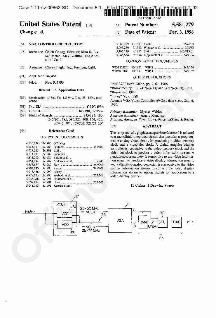
Case 1:11-cv-00862-SD Document 5-1 Filed 10/13/11 Page 29 of 65 PageID #: 92. 111111111111111111111111111111111111111111111111111111111111111111111111111
United States Patent [19]
Chang et al.
[54] VGA CONTROLLER CIRCUITRY
[75] Inventors: Chieh Chang, Belmont; Man S. Lee, San Mateo; Alex Lushtak, Los Altos, all of Calif.
[73] Assignee: Cirrus Logic, Inc., Fremont, Calif.
[21] Appl. No.: 147,456
[22] Filed: Nov. 5, 1993
Related U.S. Application Data
[63] Continuation of Ser. No. 811,944, Dec. 23, 1991, abandoned.
[51] Int. CI.6 ....................................................... G09G 5/36
[52] U.S. CI •............................................. 345/190; 395/507 [58] Field of Search ..................................... 3451132, 190,
[56]
4,626,839 4,633,441 4,727,363 4,811,007 4,811,240 4,851,892 4,858,175 4,894,646 4,918,436 4,978,633 5,036,216 5,039,884 5,043,713
3451201, 185; 395/325, 400, 164, 425; 357/45,201; 2571203; 328/63, 104
References Cited
U.S. PATENT DOCUMENTS
1211986 O'Malley. 1211986 Ishimoto ................................. 365/189 211988 Ishii. 3/1989 Schreiber. 3/1989 Ballou et al .. 7/1989 Anderson et al ......................... 357/45 8/1989 Sato ........................................ 257/203 1/1990 Ryman .................................... 345/201 4/1990 Johary.
1211990 Seefeldt et al. ......................... 2571203 7/1991 Hohmann et al .. 811991 Ham ........................................ 257/203 8/1991 Katsura et al ..
17
PCLK r--:-=~-+-..:2;5 - 50 MHz
_~14~M~H~Z~ __ ~ __ ~1 MCLK--~~ 35
I L~4--r--VCLK ----l
33 25-75 MHz
USOO5581279A
[11] Patent Number:
[45] Date of Patent:
5,581,279 Dec. 3, 1996
5,063,429 5,095,280 5,105,179 5,345,554
11/1991 Crafts ...................................... 257/203 3/1992 Wunner et al ............................ 328/63 4/1992 Smith ................................. 340/815.01 9/1994 Lippincott et al ...................... 345/164
FOREIGN PATENT DOCUMENTS
W0/9115841 10/1991 WIPO .................................... 345/164 W091/15841 10/1991 WIPO .................................... 3451132
OTHER PUBLICATIONS
"PEGA2" User's Guide, pp. 2-61, 1986. "Brooktree" pp. 1.2, (4.7)-(4.13) and (4.57)-(4.63), 1991. "Brooktree" 1989. "inmos" Nov. 1988. Acumos VGA Video Controller AVGAI data sheet, Scpo 6, 1990.
Primary Examiner-Ulysses Weldon Assistant Examiner-Amare Mengistu Attorney, Agent, or Firm-Lowe, Price, LeBlanc & Becker
[57] ABSTRACT
The "chip set" of a graphics adapter interface card is reduced to a monolithic integrated circuit that includes a programmable analog clock circuit for producing a video memory clock and a video dot clock. A digital graphics adapter controller is responsive to the video memory clock and the video dot clock to produce a video information stream. A random-access memory is responsive to the video information stream to produce a video display information stream, and a digital-to-analog converter is responsive to the video display information stream to convert the video display information stream to analog signals for application to a video display device.
11 Claims, 2 Drawing Sheets
11
VGA
~------~y~------~
23

Case 1:11-cv-00862-S
D D
ocument 5-1 F
iled 10/13/11 Page 30 of 65 P
ageID #: 93
15
VIDEO RAM /30
- ---- 1 r - - 11 I I I I PCLK VGA ~I _--,
I I
19~ 23 I I ___ J L ______ _
EPROMI'13 Fig. 1
CPU BUS
17
PCLK 11
8 25-50MHz MCLK 35 14MHz
I VGA
33
Fig. 2
I 21
MONITOR
24
DAC r
Y I
23
~ • 00 • ~
~ = f"'to-
~
~ ~(,M
~ \C \C ~
r:I.l ::r a ~
o ..., N
til -.. til oc ~ -.. N ......:J \C

Case 1:11-cv-00862-SD Document 5-1 Filed 10/13/11 Page 31 of 65 PageID #: 94
u.s. Patent Dec. 3, 1996 Sheet 2 of 2
30
16 37
MCLK SEQUENCER 38 23 /' J)
CPU ~F
t---41
I ~ VIDEO VCLK ~ CONTROLLER
1~
'"'- CRT CONTROLLER
Fig. 3
AVDD FILTER AVSS
~
~32 45
Fig. 4A
RAM DAC
J
r----39
LOGIC 50
110
Fig. 4
5,581,279
30
lIO
43

Case 1:11-cv-00862-SD Document 5-1 Filed 10/13/11 Page 32 of 65 PageID #: 95
5,581,279 1
VGA CONTROLLER CIRCUITRY
This application is a continuation of application Ser. No. 07/811,944, filed Dec. 23,1991 now abandoned.
2 stream. A random-access memory is responsive to the video information stream to produce a video display information stream, and a digital-to-analog converter is responsive to the video display information stream to convert the video dis-
BACKGROUND OF THE INVENTION
1. Field of the Invention
5 play information stream to analog signals for application to a video display device. Precautions are taken to avoid interference of the digital signals of the digital graphics adapter controller with the analog signals of the programmable analog clock circuit. The present invention relates to graphic display control
lers and, more particularly, to integrated circuits that imple- 10
ment graphics display controllers and programmable clock signal generators.
2. State of the Art In the field of computer graphics, the prevailing present-
15 day standard is the VGA standard, which specifies a 640x 480 pixel display format. To implement that standard, conventional practice has been to use a VGA video interface card to interface a computer to a high-resolution display device. A VGA interface card is typically built around a
20 VGA "chip set" that includes a number of complementary chips proven to work well together and that together realize all of the necessary functions to drive the display device. Reduction of the number of chips in the chip set simplifies manufacture, reduces cost and increases reliability.
In some VGA interface cards of the prior art, the chip set has included a programmable clock signal generator chip, or "P clock". An example of such a P clock chip is the Dual VideolMemory Clock Generator ICS90C64 manufactured
25
by Integrated Circuit Systems, Inc. of Valley Forge Pa. A P 30
clock chip simultaneously generates two clock signals. One clock signal is for the video memory used to store display information, and the other clock signal is used as the video dot clock signal, or pixel clock. Each cycle of the pixel clock, signals are produced to display one pixel on the 35
display screen.
BRIEF DESCRIPTION OF THE DRAWINGS
FIG. 1 is a functional block diagram of a VGA interface including the VGA controller chip of the present invention;
FIG. 2 is a functional block diagram showing in greater detail the P clock portion of the VGA controller chip of the present invention;
FIG. 3 is a functional block diagram showing, in greater detail, the VGA controller chip of the present invention; and
FIGS. 4 and 4A are a plan diagram showing layout details of the VGA controller chip of the present invention.
DETAILED DESCRIPTION OF THE PREFERRED EMBODIMENTS
Referring now to FIG. 1, a VGA controller 11 operating according to program instructions stored in an EPROM 13 or other program memory reads and writes video information to and from a video RAM 15. Timing signals for the VGA controller 11 are provided by a P clock 17. The VGA controller 11 is connected to the CPU bus 19 such that the CPU may exercise supervisory control over the VGA controller 11. To display video information on a video monitor 21, the VGA controller 11 reads video information from the video RAM 15 and produces a video information stream that is output to a random access memory in combination with a digital-to-analog converter, together referred to as a RAMDAC. Using information stored in the RAM portion of the RAMDAC 23, the video information corresponding to each
40 individual pixel is translated into video display information, for example the values of R, G and B signals required to display the pixel as desired. The R, G and B values are then converted to analog signals in the DAC portion of the RAMDAC 23, and output to the display monitor 21.
other than P clock chips, chips are also available to generate the video dot clock only, i.e. V clock chips. An example of one such chip may be found in U.S. Pat. No. 5,036,216, incorporated herein by reference. Clock chips of the type referred to are essentially frequency generators and are designed such that the frequency generated may be selected from among a set of predetermined frequencies that includes frequencies suitable for most common applications. The clock chips are therefore programmable in the narrow 45
sense that their operating frequency can be selected. (The word "programmable" as it appears herein is used in the foregoing sense unless other indicated.)
The primary chip in a VGA chip set is typically a large, sophisticated, digital VGA controller chip manufactured using VLSI techniques. By contrast, P clock chips are comparatively small and are at least partly analog in order to perform the function of frequency generation. Therefore, despite the pressure to reduce chip count, the P clock chip and the VGA controller chip have been unlikely candidates for integration.
SUMMARY OF THE INVENTION
The present invention generally provides a "chip set" for a graphics adapter interface card where the chip set is effectively reduced to a single chip, or monolithic integrated circuit. The monolithic integrated circuit includes a programmable . analog clock circuit for producing a video memory clock and a video dot clock. A digital graphics adapter controller is responsive to the video memory clock and the video dot clock to produce a video information
As will now be described, the VGA controller 11, the RAMDAC 23 and the P clock 17 are all integrated on a single hybrid integrated circuit chip 30. Integration of the VGA controller and the RAMDAC 23 has been achieved in the prior art. Since the VGA controller is exclusively digital,
50 and the RAMDAC 23 is largely digital such an integration does not impose any inherent difficulties. The analog portion of the RAMDAC, namely the analog part of the digital-toanalog converter, produces only DC voltages, which are relatively immune to interference from digital signals. Digi-
55 tal-to-analog converters have of course been integrated for many years.
Despite the pressure to reduce chip count, however, the P clock and the VGA controller have been unlikely candidates for integration on a single chip. One formidable obstacle has
60 been that the P clock necessarily includes high-frequency analog components that are easily susceptible to interference from digital signals. Furthermore, a VGA controller chip is large and complex and represents a significant research and development expenditure. A P clock is comparatively small.
65 Because of the perceived incompatibility of the two devices for integration, conventional wisdom has been that to attempt to integrate the P clock and the VGA controller

Case 1:11-cv-00862-SD Document 5-1 Filed 10/13/11 Page 33 of 65 PageID #: 96
5,581,279 3
would be folly inasmuch as the small P clock with its analog circuitry would endanger operation of the large complex VGA controller.
4 17 but also the RAMDAC 23. In certain modes of operation, it may be desirable for the VGA controller 11 to bypass the RAM portion of the RAMDAC 23 and instead provide video display information directly to the DAC portion of the The aforementioned reluctance to consider the P clock
and the VGA controller as legitimate candidates for integration has obscured numerous significant advantages that can be achieved by a monolithic integration. A particular advantage of integrating the VGA controller 11, the RAMDAC 23 and the P clock 17 on a single chip (as shown in FIG. 1) is that true programmability of the P clock as opposed to mere frequency selectability may be greatly facilitated. The rate at which the VGA controller 11 reads video information from the video RAM 15 and the rate at which the VGA controller sends video information to the RAMDAC 23 may be different. Furthermore, these two rates may be required to vary widely according to the particular display requirements. The memory clock, or MCLK, according to which the VGA controller 11 accesses the video memory 15 may have a frequency ranging from 25 MHz to
5 RAMDAC 23 through a selector 24. In order to support 18/24 bit color mode, if the RAMDAC 23 were not integrated with the VGA controller 11, 24 additional output pins would have to be provided on the VGA controller chip, which would render the VGA controller chip economically
10 unfeasible. By integrating the VGAcontroller and the RAMDAC 23, corresponding signal lines may be run on chip such that 18/24 bit color mode may be supported with no pin count penalty.
As shown in FIG. 3, the RAMDAC 23 is integrated on-chip. In addition, the P clock, composed of an MCLK
15 portion 16 and a VCLK portion 18, is integrated on-chip.
50 MHz, for example, in typical applications. The video dot clock or VCLK, according to which the VGA controller 11 supplies video information the RAMDAC 23 may have a similar frequency range.
The MCLK block 16 supplies an M clock to a sequencer 27 that controls reading and writing to and from the video memory. The VCLK block 18 supplies a V clock or video dot clock to a CRT controller 38, a video controller 39, and
20 the RAMDAC 23. The CRT controller contains various
Referring to FIG. 2, the P clock generates the M clock and V clock using two analog voltage-controlled oscillators (VCOs) 31 and 33 each incorporated in a phase-locked loop. 25 The phase-locked loops receive a reference frequency from the computer mother board, approximately 14 MHz in IBM-compatible computers. In accordance with the prior art, frequency selectability is achieved by incorporating variable dividers into the phase-locked loops. Pre-pro- 30 grammed devisors are loaded into the variable dividers according to frequency selection signals 35 from the VGA controller. To achieve true programmability, the devisors that may be used in the phase-locked loops would not be limited to some number of pre-programmed devisors but 35
would instead be arbitrarily specified by the VGA controller
counters such as a line counter, a pixel counter, and a frame counter together with associated logic for controlling the actual video display of information. The video controller 39 formats memory data (according to selected display modes) and sends the video data to the RAMDAC. A CPU interface 41 allows the host computer to exercise supervisory control.
As mentioned previously, potential interference of the VGA controller's digital signals with the analog signals of the P clock poses a distinct threat to circuit performance. This threat may be negated using strategic design measures as illustrated in FIG. 4. In addition to digital power and ground signals VDD and VSS, analog power and ground signals AVDD and AVSS are separately provided. A logic portion 50 of the VGA controller chip 30 occupies an interior region of the chip, and I/O cells 43 including analog and digital I/O cells, are provided around the periphery of the chip (the wafer substrate) to allow for input of external signals to the chip 30 and output of internal signals from the
to some precision within a wide allowable range. As different graphical standards and formats evolve, the system would then be adapted by simply changing the program of the VGA controller 11 stored in the EPROM 13.
True programmability, however, requires a considerably more complex interface between the VGA controller 11 and the P clock 17 than simple frequency selectability, requiring
40 chip.
in tum an increased number of signal lines between the two devices. By integrating the P clock 17 and the VGA con- 45
troller 11 on a single chip, the signals necessary to achieve true programmability may be placed on chip. With the P clock and the VGA controller on separate chips, the alternative would be to attempt to increase the already-large pin count of the VGA controller chip to make additional signal 50
lines available, a dubious undertaking at best.
By integrating the P clock 17 and the VGA controller 11 such that the interface signal lines between the two devices are placed on chip, further advantages are achieved. Less power is required to drive the signal lines (an important 55
consideration in notebook applications) and less electromagnetic radiation is produced, making EC.C. approval easier. With the two devices on separate chips, powerful signal drivers must be provided to drive signals between the two chips along traces on a printed circuit board, increasing 60
radiation and the precautions necessary to achieve EC.C. compliance. With the P clock 17 and the VGA controller 11
Another important feature of the above-described monolithic integration is that the analog I/O cells are at least partially grouped together and the voltage controlled oscillators of the P clock (31 and 33 in FIG. 2) are formed at least partially within an analog I/O cell located in between two other analog I/O cells. This situation is depicted in the enlarged area FIG. 4, representing a magnified view of a portion of three adjacent analog I/O cells 45. Seen in the magnified area are three I/O pads to which signal pins are to be bonded, an AVDD pad, a FILTER pad and an AVSS pad. AVCO portion 32 of one of the MCLK and the VCLK is laid out in an area of the chip adjacent the FILTER pad, in between the AVDD and AVSS pads. The VCO portion 32 of the clock is therefore located apart from a digital portion of the clock and close to the FILTER signal required by the VCO 32. Furthermore, the next closest inputs, AVDD and AVSS, are both stable DC inputs, which do not cause interference for the high-frequency VCO. The other VCO is similarly located adjacent its corresponding FILTER input and is flanked by separate AVDD and AVSS pads.
Therefore, the above-described monolithic integration provides a complete VGA solution in the form of a fullyintegrated VGA controller chip. By integrating both the RAMDAC 23 and the P clock on-chip, total pin count may
on the same chip, radiation levels may be sufficiently reduced to allow a two layer printed circuit board to be used rather than a four layer printed circuit board.
Significant advantages are also achieved by integrating on a single chip with the VGA controller 11 not only the P clock
65 be significantly reduced. Radiation levels may also be significantly reduced, making board design and regulatory approval much easier. Most significant, integration of the

Case 1:11-cv-00862-SD Document 5-1 Filed 10/13/11 Page 34 of 65 PageID #: 97
5,581,279 5
VGA controller and the P clock renders the prospect of true programmability of the P clock technically feasible.
6
The foregoing has described the principles, preferred embodiments and modes of operation of the present invention. However, the invention should not be construed as 5
limited to the particular embodiments discussed. Instead, the above-described embodiments should be regarded as illustrative rather than restrictive, and it should be appreciated that variations may be made in those embodiments by workers skilled in the art without departing from the scope 10
of present invention as defined by the following claims.
video memory clock signal and the video dot clock signal and for producing a video information data stream;
random-access memory means, coupled to said video controller, for receiving the video information data stream and producing a video display information data stream;
digital-to-analog converter means, coupled to said random-access memory means, for receiving the video information data stream and converting the video information data stream to analog video signals; and
What is claimed is: 1. A monolithic integrated circuit comprising:
programmable memory means coupled to the monolithic integrated circuit for storing said devisor data to be received by the programmable clock circuit means. programmable clock circuit means for producing a video
memory clock signal and a video dot clock signal; 15 6. The arrangement of claim 5, wherein the video memory clock has a frequency selected from among 37.58523 MHz, 41.74431 MHz, and 50.11363 MHz.
a video controller coupled to said programmable clock circuit means for receiving the video memory clock signal and the video dot clock signal and for producing a video information data stream;
random-access memory means, coupled to said video controller, for receiving the video information data stream and producing a video display information data stream; and
digital-to-analog converter means, coupled to both said random-access memory and to said video controller, for selectively receiving either the video information data stream or the video display information data stream as received data and for converting the received data to analog video signals.
2. The monolithic integrated circuit of claim 1, wherein said video information data stream comprises a stream of pixel data having twenty-four bits per pixel and said digitalto-analog converter means comprises three digital to analog converters.
3. The monolithic integrated circuit of claim 1, wherein said video information data stream comprises a stream of pixel data having eighteen bits per pixel and said digital-toanalog converter means comprises three digital to analog converters each for receiving six data bits.
4. The monolithic integrated circuit of claim 1, wherein said video information data stream comprises a stream of pixel data having at least eight data bits per pixel.
5. An arrangement comprising: a monolithic integrated circuit having:
programmable clock circuit means for recelvlllg a reference clock signal and devisor data and for dividing said reference clock signal by said devisor data to produce a video memory clock signal and a video dot clock signal;
a video controller coupled to said programmable clock circuit for providing said programmable clock circuit means with said devisor data and for receiving the
7. The arrangement of claim 5, wherein the video dot clock signal has a frequency selected from among 25.1802
20 MHz, 28.3251 MHz, 41.1648 MHz. 36.0818 MHz, 31.193 MHz, 39.992 MHz, 44.907 MHz, 50.113 MHz, 64.982 MHz, and 75.169 MHz.
8. The arrangement of claim 5, wherein said programmable memory means may be selectively programmed with
25 devisor data so as to selectively alter the frequency of said video memory clock signal and said video dot clock signal.
9. A monolithic integrated circuit comprising:
30
35
40
45
a programmable clock circuit responsive to a reference clock signal and devisor data and generating a video memory clock signal and a video dot clock signal;
a video controller receiving the video memory clock signal and the video dot clock signal and producing a video information data stream from data received from a video RAM;
a random-access memory producing a video display information data stream in response to the video information data stream from said video controller;
a digital-to-analog converter converting received digital data to analog video signals; and
a selector supplying one of said video information data stream from the video controller and said video display information data stream from said random-access memory to said digital-to-analog converter as said received digital data.
10. A circuit as recited in claim 9, wherein the devisor data is supplied to said programmable clock circuit from the video controller.
11. A circuit as recited in claim 10, wherein the video 50 controller supplies the devisor data in response to program
instructions retrieved from a programmable memory.
* * * * *

Case 1:11-cv-00862-SD Document 5-1 Filed 10/13/11 Page 35 of 65 PageID #: 98
UNITED STATES PATENT AND TRADEMARK OFFICE
CERTIFICATE OF CORRECTION
PATENT NO. 5,581,279
DATED December 3, 1996
INVENTOR(S) Chang e tal.
It is certified that error appears in the above-indentified patent and that said Letters Patent is hereby corrected as shown below:
Column 1, line 37, delete "other" and insert --Other..,..-.
Column 4, line 19, delete "CRT controller 38, a video controller 39" and
insert --CRT controller 39, a video controller 38--.
Column 4, line 24, delete "video controller 39" and insert
--video controller 38--.
Attest:
Attesting Officer
Signed and Sealed this
Nineteenth Day of August, 1997
BRUCE LEHMAN
Commissioner of Patents and Trademarks

Case 1:11-cv-00862-SD Document 5-1 Filed 10/13/11 Page 36 of 65 PageID #: 99
PATENT NO.
DATED
INVENTOR(S)
UNITED STATES PATENT AND TRADEMARK OFFICE
CERTIFICATE OF CORRECTION
5,581,279
December 3, 1996
Chang et al.
It is certified that error appears in the above-identified patent and that said Letters Patent is hereby corrected as shown below:
Column 6, line 9, after Ilvideo" insert --display--; and line 10, after "video" insert --display--.
Attest:
Attesting Officer
Signed and Sealed this
Twenty-fIfth Day of May, 1999
Q. TODD DICKINSO:"l
Acting Commissioner (~f Pate,,,.\" and Trademark.\

EXHIBIT 3
Case 1:11-cv-00862-SD Document 5-1 Filed 10/13/11 Page 37 of 65 PageID #: 100

Case 1:11-cv-00862-SD Document 5-1 Filed 10/13/11 Page 38 of 65 PageID #: 101
(12) United States Patent Keene
(54) HARDWARE ASSIST FOR YUV DATA FORMAT CONVERSION TO SOFTWARE MPEG DECODER
(75) Inventor: David Keene, San Mateo, CA (US)
(73) Assignee: S3 Graphics Co., Ltd., Cayman Islands (KN)
( *) Notice: Subject to any disclaimer, the term of this patent is extended or adjusted under 35 U.S.c. 154(b) by 0 days.
(21) Appl. No.: 09/430,370
(22) Filed: Oct. 29, 1999
Related U.S. Application Data
(63) Continuation of application No. 08/619,203, filed on Mar. 21, 1996, now Pat. No. 6,005,546.
(51) Int. CI? .................................................. G09G 5/04 (52) U.S. CI. ....................... 345/603; 345/531; 345/520;
345/547; 345/562 (58) Field of Search ................................. 345/154, 186,
(56)
345/501, 523-525, 155, 434, 203, 530-535, 547, 545, 572, 603-604, 520, 562; 348/453,
717,384
References Cited
U.S. PATENT DOCUMENTS
5,136,379 A 5,341,175 A 5,428,389 A 5,446,860 A 5,450,130 A 5,459,516 A 5,461,420 A 5,469,228 A 5,488,432 A 5,489,942 A 5,495,291 A 5,500,577 A 5,502,503 A 5,526,025 A 5,553,220 A
8/1992 Ishii ........................... 358/138 8/1994 Koz ........................... 348/552 6/1995 Ito et al. ..................... 348/231 8/1995 Dresser et al. .............. 395/427 9/1995 Foley ......................... 348/391
10/1995 Song .......................... 348/402 10/1995 Yonemitsu et al. ......... 348/401 11/1995 Kim et al. .................. 348/715
1/1996 Guillon et al. .............. 348/717 2/1996 Kawahara ................... 348/401 2/1996 Adams ....................... 348/390 3/1996 Kim et al. .................. 315/364 3/1996 Koz ........................... 348/552 6/1996 Selwan et al. .............. 345/200 9/1996 Keene ........................ 395/154
111111 1111111111111111111111111111111111111111111111111111111111111
EP EP
US006353440Bl
(10) Patent No.: US 6,353,440 BI Mar. 5,2002 (45) Date of Patent:
5,604,514 A 5,611,041 A 5,642,139 A 5,654,773 A 5,666,137 A 5,699,277 A 5,815,168 A 5,874,995 A 6,005,546 A 6,067,098 A 6,107,987 A
2/1997 Hancock ..................... 345/154 3/1997 Bril et al. ................... 395/507 6/1997 Eglit et al. .................. 345/202 8/1997 Kajimoto et al. ........... 348/717 9/1997 Coelho et al. .............. 345/155
12/1997 Munson et al. ............. 364/514 * 9/1998 May ........................... 345/516 * 2/1999 Naimpally et al. ......... 348/384 * 12/1999 Keene ........................ 345/154 * 5/2000 Dye ........................... 345/531 * 8/2000 Coelho ....................... 345/154
FOREIGN PATENT DOCUMENTS
797181 A2 9/1997 G09G/1/16 797181 A3 1/1998
OTHER PUBLICATIONS
Undy S. et al. "A Low-Cost Graphics and Multimedia Workstation Chip Set", vol. 14, No.2, pp. 10-22, IEEE Micro, Apr. 1994. Lee, Ruby B. et aI., "Real-Time Software MPEG Video Decoder on Multimedia-Enhanced PA 7100LC Processors", vol. 46, No.2, pp. 60-68, Hewlett-Packard Journal, Apr. 1995.
* cited by examiner
Primary Examiner-Richard Hjerpe Assistant Examiner---firancis Nguyen (74) Attorney, Agent, or Firm-Carr & Ferrell LLP
(57) ABSTRACT
A display controller assists a host processor in decoding MPEG data. The display controller receives YUV data in non-pixel video format from a host CPU and perform the otherwise CPU intensive task of rasterization within the display controller. In addition, the display controller may use its internal BITBLIT engine to copy U and V data from one line in a BITBLIT operation to adjacent lines, so as to replicate U and V data. A byte mask preserves Y data on the adjacent lines from being overwritten. At the end of the BITBLIT operation, the display controller generates a signal indicating that the frame buffer has been filled with new data, and thus display controller automatically switches to reading from the newly written frame buffer.
27 Claims, 8 Drawing Sheets

Case 1:11-cv-00862-SD Document 5-1 Filed 10/13/11 Page 39 of 65 PageID #: 102
u.s. Patent Mar. 5, 2002 Sheet 1 of 8
vv ... 1 v
,,-
y
F-igtLre lA (Prior A.rt)
DWORD GRAPHICS ..... ,
\ u "-
y V
VIDEO 1
VIDEO 2
Fig'ure lB (Prior Art)
US 6,353,440 BI
~201 y ....
I'---- 202
t---- 203

Case 1:11-cv-00862-SD Document 5-1 Filed 10/13/11 Page 40 of 65 PageID #: 103
U.S. Patent Mar. 5, 2002 Sheet 2 of 8
l.3JL
LINE 1
LINE 2
UNE 3
~~~'i j
1
Y
y
Y j
I U y.1 V
* y
U Y I I
1 I I
• I j
I J • I I
I f
Fig'ure lC (Prior Art)
* V
US 6,353,440 BI
I Y I X
Y j l
t J
1 'J
•

Case 1:11-cv-00862-SD Document 5-1 Filed 10/13/11 Page 41 of 65 PageID #: 104
U.S. Patent
-\
1
Mar. 5,2002
/""'\ ~'f. '\, -r
!
-,/
,/~..../I
Sheet 3 of 8
-
1 1 1\/
I :e j f.' I >o-f < ...J I • .J . ~o - .I'WI
~c::
=:c: I .... 0 .~
I I I I
1 l-e:: v
0 C"'oe -/
<:) ao
/
US 6,353,440 BI
".-... ..,.. N • -~ < • - , - -- .... e.£ '-.-.- , r~ -- ,--......

Case 1:11-cv-00862-SD Document 5-1 Filed 10/13/11 Page 42 of 65 PageID #: 105
u.s. Patent Mar. 5,2002
o
\ -\ I
- I Ul
~/
Sheet 4 of 8
o 0:::1
US 6,353,440 BI
~ • ---CJJ .-~

Case 1:11-cv-00862-SD Document 5-1 Filed 10/13/11 Page 43 of 65 PageID #: 106
u.s. Patent
.~ 15M /
/
Ii \ j
\ I
I 15M ~
\ ~
'Z I .<
) ~
I ~ / (fl 410 "\ ::J \ 14M
I , ;::::: I c I c I < !
I I
>- I c.; \
:. \ 13M \ I
\
\ \ 12M
Mar. 5,2002 Sheet 5 of 8
_':l_~~
'il Data (256 Kilo-Bytes)
I t
__ I ~ ~-
U Data f ..... --\ ,,':::lfJ Kilo-Bytes)
Y Data (512 Kilo-Bytes)
V Data (256 Kilo-Bytes)
u Data (256 Kilo-Bytes)
y Data (512 Kilo-Bytes)
V Data (256 Kilo-Bytes)
u Data (256 Kilo-Bytes)
y Data (512 Kilo-Bytes)
V Data (256 Kilo-Bytes)
u Data (256 Kilo-Bytes)
y Data (512 Kilo-Bytes)
Figure 4
US 6,353,440 BI
+ "\
j
I 1 414
r Meg
• ''\
\ I \ i { :n , i Q1
tl ~ 413 ~ ,..
I c. Meg c.
I < ;-
j ~ ) :.
t \ ~
'1 c
! ,.
I z ;-
\ :. 412 ~ -<
1 Meg i ::c I
;.:J I
~
+
! -)
\ I I I I 411 ,> 1 Meg I I
! I I i ..-
ill

Case 1:11-cv-00862-SD Document 5-1 Filed 10/13/11 Page 44 of 65 PageID #: 107
u.s. Patent
g Ilol i-:J' Vl « C a:: a.. w a: I a:: ~ ........ I--'~,.. ... l a: ..J w « ~ a: .J Ilol « ffi r---~o_i g (,:J .J
I T
c <D :::In
0 c::: (,/)
0 I.
cc
Mar. 5,2002 Sheet 6 of 8
DISPLAY MEMORY CONTROLLER
I t ['
c: C 0.. (J '!.
, w a:: o (J
~ ::>
~ I
I I
l.l (,:J
~tn -a: Ow (JI)oVl a::i3 Ow ~a:1 w ~
FIGURE
\ \
C N .:"'1
US 6,353,440 BI
\ /
"
~, ... --

Case 1:11-cv-00862-SD Document 5-1 Filed 10/13/11 Page 45 of 65 PageID #: 108
u.s. Patent
LINE 3
LINE 2
LINE 1
Mar. 5,2002 Sheet 7 of 8
8 + 2P + 3 Y3,7 Y3,8
8 + 2P + 2 Y3,5 Y3,6
8 + 2P + 1 I Y3,3 Y3,4
! I IS + 2P + 0 j
Y 3,2 Y3,1 I ~_~~_~i~ ___ . _____ . ___ L ___ _
8+P+3 i Y27 I 8+P+2 Y25 ,
8+P+1 Y2,3
8+P+0 Y2,1
8+N Y1 ,Xr - 1
I
I I 8+7 Y1,15 !
S+6 i Y 1 13 i
!
S+5 ! Y1,11
8+4 Y1,9
8+3 Y1,7
8+2 Y1,5
8+1 Y1 3 ,
8+0 Y1,1
Address Byte 0
FIG. 6
I
• • •
Y 2,8
Y2,6
Y2,4
Y22 ,
Y1,Xr
• • •
Y1,16
Y114 +----~ I
Y1,12
Y1 10 ,
Y1 8
Y1 6 ,
Y1 4 ,
Y1 2 ,
Byte 1
US 6,353,440 BI
i
V2,4 U24 I
I V2,3 U2,3 I
V2,2 U2,2 --,
V2,1 ! U2,1
i ! I
V1,4 U1,4 I
V1,3 U1 3 ,
V1,2 U1,2
V1,1 U1,1
V1,Xr/4 U1,Xr/4
I I I
V1,8 U1,8 I i V1 7
I u171 I I I ' I
I V1 6 U1,6 I
V1,5 U1,5
V1 4 U1,4
V1,3 U1,3
V1,2 U1 2
V1,1 U1,1
, Byte 2 Byte 3
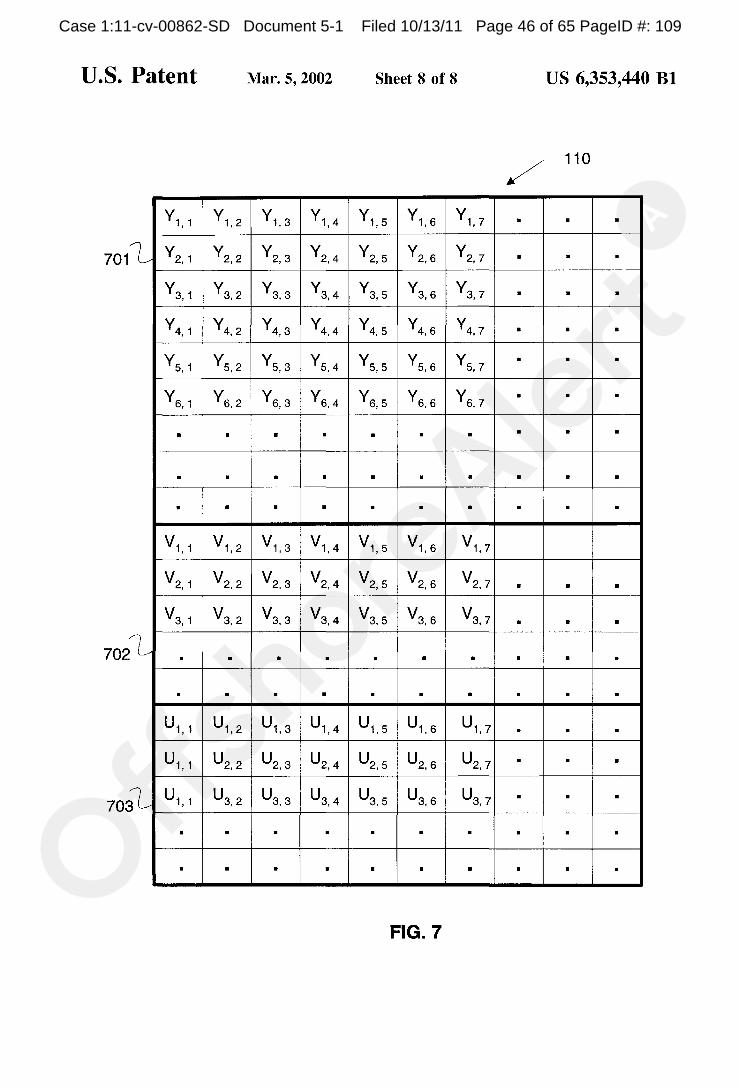
Case 1:11-cv-00862-SD Document 5-1 Filed 10/13/11 Page 46 of 65 PageID #: 109
u.s. Patent Mar. 5,2002 Sheet 8 of 8 US 6,353,440 BI
110
Y1,1 Y1 2 Y1,3 Y1,4 Y1,s Y1 6 Y1,7 • · •
701 L Y2,1 Y2,2 Y23 Y24 Y2,s Y26 Y2,7 • • · Y3,1 Y3,2 Y3,3 Y3,4 Y3,s Y3,6 Y3,7 • • •
Y4,1 Y4,2 Y4,3 Y44 Y4,s Y4,6 Y4,7 • • •
YS,1 YS,2 YS,3 YS,4 Ys,s YS,6 YS,7 · · · Y6,1 Y6,2 Y6,3 Y6,4 Y6, S Y6,6 Y67 • · ·
• • • · · · · · · · · · · • · · • · · · • • · · · · · · · ·
V 1,1 V 1 2 , V 1,3 V 1,4 V 1, S V 1,6 V 1,7
V 2 1 V 2,2 V 23 V 2,4 V 2,s V 2,6 V 2,7 • • •
V3 1 V 3,2 V33 V 3,4 V 3. S V 3,6 V 3,7 · · · 702 ~L · . . · . • . • • ·
· · · · · · · · · · U1,1 U1 2 , U1 3 , U1,4 U1,s U1 6 U1,7 · · · U1,1 U2,2 U2,3 U24 U2,s U26 U2,7 · · • ,
703 ;L U1,1 U32 U33 U3,4 U3,s U3,6 U3,7 · · · • · · · · · · · · · · · · • • • • · · ·
FIG. 7

Case 1:11-cv-00862-SD Document 5-1 Filed 10/13/11 Page 47 of 65 PageID #: 110
US 6,353,440 Bl 1
HARDWARE ASSIST FOR YUV DATA FORMAT CONVERSION TO SOFTWARE
MPEG DECODER
RELATED APPLICATION
This application is a continuation of U.S. patent application Ser. No. 08/619,203, filed on Mar. 21, 1996 now U.S. Pat. No. 6,005,546.
FIELD OF THE INVENTION
2 decoding (or the like) entirely within software operating within host CPU 110. For example, future versions of Microsoft® Windows 95™ may include such MPEG decoding software. Intel® also offers a software video decoding
5 technique under the trademark Indeo TM. Applications software or operating systems (e.g., Win
dows™ 95) may be provided with such MPEG or Indeo™ decoding software. Placing MPEG or Indeo ™ decoding software within applications software or an operating system
10 may allow a user to view video portions on a display screen without the need for purchasing additional hardware such as dedicated MPEG hardware decoder 140. The present invention relates to an apparatus and method
for generating a display image including video portions. In particular, the apparatus and method of the present invention may be utilized to assist a software embodied MPEG 15
(Motion Picture Encoding Group) decoder to generate video
However, even with high performance microprocessors, decoding of MPEG data may be a host CPU intensive operation, which may degrade overall performance of computer system 100. A large portion of host CPU cycles required to implement MPEG decoding may be required for data transfer and formatting, rather than decoding per se.
images.
BACKGROUND OF THE INVENTION
Personal computers may be used to generate displays including video portions. For the purposes of the present application, the term "video" refers to full motion video images (e.g., derived from TV, film, video or the like) such as Cirrus Logic Motion Video ™ type displays. Motion Video Architecture (MVATM) is described, for example, in co-pending U.S. patent application Ser. No. 08/483,584, entitled "DUAL DISPLAYS HAVING INDEPENDENT RESOLUTIONS AND REFRESH DATES", filed Jun. 7, 1995 and incorporated herein by reference. Such video portions may be generated from a data source (e.g., CD-ROM) where video data may be encoded in one of a number of formats (e.g., MPEG-I, MPEG-II, Indeo™ or the like).
MPEG data may be decoded and decompressed (in soft-20 ware and/or hardware) from an MPEG data source in several
steps. Host CPU 110 (or dedicated MPEG decoder 140) may retrieve compressed/encoded MPEG data from an MPEG data source (e.g., CD-ROM or the like) and first perform a Huffman decoding, followed by inverse quantization of data,
25 inverse DCT (Discrete Cosine Transform), and motion compensation (compression between frames). For software MPEG decoding, a 90 MHz Pentium™ microprocessor may be just barely able keep up with these first four steps at a rate of 30 frames per second.
30 Once decoded and decompressed, MPEG data in YUV
format may be transferred from component YUV video (i.e., planar form) to a pixel video format (i.e., raster scan format).
Traditionally, MPEG decoding may be performed by a 35
dedicated hardware decoder. A hardware MPEG decoder
The pixel video YUV data may then be converted from YUV to RGB (Red, Blue and Green pixel data) and then stored in display memory 130 to be displayed on display 180. Prior art
may receive MPEG encoded data from a data source (e.g., CD-ROM) and output YUV data to discrete portions of display memory of a display controller, as illustrated in FIG. 2.
FIG. 2 is a block diagram illustrating major components of a computer system 100 provided with display controller 120 (e.g., Video Graphics Adapter (VGA), Super VGA (SVGA) or the like). Display controller 120 may generate pixel data for display 180 (e.g., CRT, fiat panel display or the like) a t a rate characteristic of the refresh rate of display 180 (e.g., 60 Hz, 72 Hz, 75 Hz, or the like) and horizontal and vertical resolution of a display image (e.g., 640x480 pixels, 1024x768 pixels, 800x600 pixels or the like). A continuous stream of pixel data may be generated by display controller 120 at the characteristic rate of display 180.
Display controller 120 may be provided with a display memory 130 which may store pixel data in text, graphics, or video modes for output to display 180. Host CPU 110 may be coupled to display controller 120 through bus 150 and may update the contents of display memory 130 when a display image for display 180 is to be altered. Bus 150 may comprise, for example, a PCI bus or the like. System memory 160 may be provided coupled to Host CPU 110 for storing data.
Hardware MPEG decoder 140 may be provided to decode MPEG video data from an MPEG video data source (e.g., CD-ROM or the like) and output decoded video data to system memory 160 or directly to display memory 130. However, with the advent of increasingly powerful and faster microprocessors (e.g., Pentium™ or PowerPCTM processor or the like) it may be possible to implement MPEG
hardware video accelerators may handle the YUV to RGB conversion step to remove that task from host CPU 110. However, the step of formatting YUV component data to
40 pixel video form may still be required. Formatting YUV component data to pixel video form may
require host CPU 110 (for hardware MPEG decoding, MPEG decoder 140) to decode MPEG data, as discussed above into a YUV 4:2:2 video format (i.e., CCIR 601
45 format) where groups of two pixels may be encoded as two bytes of luminance (Y) data as well as two bytes of chrominance difference (U,V) data. Display 180 and display controller 120 may require that output data be generated in a basic pixel video (i.e., scan line) format such that all data
50 (e.g., RGB or YUV) for each output pixel located in consecutive locations within display memory 130.
In a YUV 4:2:2 format, two bytes of Y data may be followed by one byte of U data and one byte of V data. Each double word (DWORD) read out may thus comprise infor-
55 mation for two adjacent pixels of data which may be read by display controller 120 in sequential addresses to be consistent with pixel video methods of display and make best use of available memory bandwidth.
Prior art MPEG decoding techniques (hardware or 60 software) may first decompress MPEG data from an MPEG
data source (e.g., CD-ROM or the like) into separate Y, U, and v values. These Y, U, and V values may then be stored initially into separate Y, U, and V memory areas (planes) in system memory 160 as illustrated in FIG. 1A in a format
65 known as YUV planar format or component yuv. System memory 160 may comprise separate contiguous
areas of memory 102, 103 and 104 for storing Y, U and V

Case 1:11-cv-00862-SD Document 5-1 Filed 10/13/11 Page 48 of 65 PageID #: 111
US 6,353,440 Bl 3 4
negated. Upon completing a write cycle to fill one of video buffer 202 or 203, display controller 120 need be signaled to switch reading from the other of video buffers 202 and 203.
A YUV formatted DWORD may be stored in pixel video
data, respectively. For video data in the CCIR 601 format, two Y values may be provided for each U and V values to comprise pixel data for two adjacent pixels. Thus, the Y portion of system memory 160 may be twice as large as each of the respective U and V portions 103 and 104. 5 format within video buffer 202 or 203 of display memory
130. Display controller 120 may readily generate video images from pixel video YUV data stored within video buffer 202 or 203 of display memory 130.
To combine separate Y, U, and V data into a format convenient for prior art video accelerators, host CPU 110 may first read two bytes of data from system memory area 102 containing Y data and shift one of those bytes over to a different byte location within a 32 bit DWORD register 10
within host CPU 110. Next, host CPU 110 may read a byte of U data from the U area 103 of system memory 160 and then read a byte of V data from the V area 104 of system memory 160. Host CPU 110 may then combine separate Y, U, and V data into a YUV 4:2:2 formatted DWORD which 15
in turn may be transferred to display memory 130. Such byte shifting operations are not particularly efficient
for such processors as the Pentium® processor and thus system performance may be degraded, because a significant percentage of the CPU cycle would be used just for data 20
reformatting (i.e., component YUV to pixel video). Moreover, reading separate Y, U, and V data from noncontiguous portions of system memory 160 may require a large number of random access memory cycles, which will not get page cycles across the bus, further degrading system 25
performance. For a PCI bus system, it may be possible to combine
separate read cycles in an internal cache within host CPU 110. However, processor and read cycle overhead may prevent system 100 from taking full advantage of burst 30
cycles available in PCI bus architecture.
One processor intensive portion of software MPEG decoding, therefore, is the method of transferring the planes of Y, U, and V data from system memory 160 into display memory 130 in a pixel video format. Another processor intensive portion of software MPEG decoding is the need to vertically up-sample chrominance difference (U,V) data. Data encoded in an MPEG format has the same number of luminance (Y) samples (or bytes) as there are actual pixels displayed for the resulting playback. However chrominance difference samples (U and V) played back are sub-sampled both horizontally and vertically (e.g., one V and U data pair for each 2x2 block of Y data).
The MPEG encoding technique may encode pixel data from blocks of four luminance samples in a two dimensional pattern (e.g., two by two pixels) for everyone pair of chrominance difference samples (U,V). Chrominance difference samples (U,V) may actually be sub-sampled from the center point of a two by two pixel block. Upon decompression, chrominance difference data (U,V) may be replicated to create chrominance difference samples for groups of two pixels in the YUV 4:2:2 format.
FIG. 1C illustrates how horizontal and vertical subsampling may occur to create interpolated U and V values. FIG. 1C illustrates Y, U, and V values stored in display memory 130. As data is stored in display memory 130 in a
Once a YUV 4:2:2 formatted DWORD has been assembled within host CPU 110, it may then be stored in display memory 130 in a rasterized (i.e., pixel video) format as illustrated in FIG. lB. Display memory 130 may comprise graphics portion 201 for storing graphics data (e.g., Windows™ Graphical User Interface (GUI) data), and one
35 pixel video format (e.g., scan line by scan line) it may be a relatively easy task to interpolate U and V data horizontally. However, as U and V data is sub-sampled in both horizontal and vertical directions, it may be necessary to interpolate (or
or more video buffers 202 and 203 for storing video data representing full motion video images (e.g., Cirrus Logic 40
MotionVideo™ images). Two video buffers 202 and 203 may be provided to prevent generation of artifacts on display 180.
replicate) U and V data in a vertical direction. Thus, for example, as illustrated in FIG. 1C, every other
line of video data may require interpolation (or replication) of U and V data from other adjacent lines, to create U and V values to fill in the areas in indicated by the * values in FIG. Ie. Unfortunately, such vertical interpolation may be If host CPU 110 were writing into the same area of display
memory 130 simultaneously being used for generating an image on display 180, such writing action may be visible on display 180. A user might perceive CPU writes to display memory 130 as it is being painted or as tearing effect, as sometimes occurs, for example, in video games.
45 much more difficult to achieve than horizontal interpolation.
In prior art display controllers, such artifacts may be 50
eliminated by double buffering video data. Separate video buffers 202 and 203 may be provided within display memory 130 to store consecutive frames of video data. Host CPU 110 may write to one video buffer 202 within display memory 130 while data from another buffer 203 is being 55
read out to display 180. Such double buffering may not require large amounts of display memory 130, as MPEG video data may typically be rendered at a resolution of 352 by 240 pixels, which may be zoomed up to any size including full display resolution (e.g., 1024 by 768 pixels). 60
One difficulty encountered in double-buffering display data is that a mechanism must be provided to instruct host CPU 110 and display controller 120 to switch their respective write and read cycles alternatively from video buffers 202 and 203. If display controller 120 is reading display data 65
from the same video buffer 202 or 203 which host CPU 110 is writing to, the advantage of double buffering may be
Data from adjacent lines may need to be stored for later replication (or interpolation) when data for a particular line is stored in display memory 130.
Such storage of adj acent U and V values may require large amounts of memory or register space and may require cumbersome processor operations. It would be desirable, therefore, to reduce data bandwidth between host CPU 110 and display memory 130 by transferring only those chrominance difference (U,V) data decoded and perform replica-tion of such data within display controller 120.
SUMMARY OF THE INVENTION
The present invention comprises a display controller which may assist a host processor in decoding MPEG data. The display controller of the present invention may receive YUV data in non-pixel video format from a host CPU and perform the otherwise CPU intensive task of rasterization within the display controller. In addition, the display controller may use its internal BITBLIT engine (a feature common in advanced SVC-A display controllers) to copy U and V data from one line in a BITBLIT operation to adjacent lines, so as to replicate U and V data. A byte mask preserves

Case 1:11-cv-00862-SD Document 5-1 Filed 10/13/11 Page 49 of 65 PageID #: 112
US 6,353,440 Bl 5
Y data on the adjacent lines from being overwritten. At the end of the BITBLIT operation, the display controller generates a signal indicating that the frame buffer has been filled with new data, and thus display controller automatically switches to reading from the newly written frame buffer.
BRIEF DESCRIPTIONS OF IRE DRAWINGS
FIG. lA is a diagram illustrating how Y, U, and V data may be stored in system memory in a prior art software MPEG decoding scheme.
FIG. IB is a diagram illustrating how Y, U, and V data may be stored in display memory in pixel video form in a prior art software MPEG decoding scheme.
FIG. lC is a diagram illustrating how vertical interpolation of U and V data stored in display memory may be required in a prior art software MPEG decoding scheme.
FIG. 2 is a simplified block diagram of a prior art personal computer illustrating the relationship between a microprocessor, an MPEG decoder, a display controller, display memory.
FIG. 3 is a block diagram illustrating the arrangement of components in a computer system using software MPEG decoding with the display controller of the present invention.
FIG. 4 is a memory map illustrating a PCI location of a memory address range being mapped to an address range of display memory 130 of FIG. 3 for storing component YUV data.
6 In prior art PCI bus display controller devices, it is known
to request 16 megabytes worth of address space, even though most display controllers may use only four megabytes of actual memory. The requested 16 megabytes may be
5 divided into four almost identical regions. Each four megabyte range of the requested 16 megabyte range may map directly to the same four megabyte physical display memory.
In the prior art, the first four megabytes of address space may be used for ordinary memory writes to display memory,
10 without altering any byte ordering. The second four megabyte range may perform a word switching byte re-ordering which may be required with some types of CPUs. In other words, if host CPU 110 were to write data to the second four megabyte range (or "aperture"), display controller 120 may
15 reorder such data on a word basis before storing to display memory 130.
Similarly, the third, four megabyte address range may perform another type of byte swapping on a DWORD basis to also compensate for byte ordering used by other types of
20 CPUs. In prior art display controller 120, the fourth four megabyte range may be reserved for future use. In any event, however, all four megabyte ranges end up mapping to the same four megabytes of physical display memory 130.
Referring now to FIG. 4, in the present invention, a 25 memory address aperture 410 may be enabled in the fourth
linear address aperture discussed above (i.e., CR3F[ 4]=1 and CR3E[3:1]=OOO) of display memory 130. Aperture 410 may be mapped to four physical megabytes of display
FIG. 5 is a block diagram of one embodiment of display 30
controller 320 of FIG. 3.
memory 130. Addresses for aperture 410 may be determined by an address set by PCI configuration register 511 containing 10H as a base address. Thus, the address range for the four megabytes of display memory may be set to range from {PCI lOH base address+ 12 megabytes} to {PCI lOH base address+ 16 megabytes -1 byte}.
FIG. 6 is a diagram illustrating storage of Y, U, and V components within display memory 130 of FIG. 3.
FIG. 7 is a diagram illustrating storage ofY, U, and V data within system memory 160 of FIG. 3.
DETAILED DESCRIPTION OF IRE INVENTION
Referring now to FIGS. 3, 4, and 5, display controller 320, coupled to PCI bus 150, may be allocated a 16 megabyte address space for its use out of the possible 4 Giga-Bytes of 32-bit addressing for the PCI bus protocol. Display control-ler 320 may be provided with a base address as part of the PCI bus protocol. Display controller 320, in the preferred embodiment, may support up to 4 megabytes of display memory 130.
Display controller 320 may be provided with byte swapping modes, as PCI bus 150 may be used with different types
35 The four megabyte fourth linear aperture 410 may be
further divided into one megabyte sections 411, 412, 413, and 414 as illustrated in FIG. 4. Each one megabyte address range 411, 412, 413, and 414 may correspond to the same 1
40 megabyte of the first or primary aperture of physical display memory 130. Within each 1 megabyte region, Y, U, and V data may be arranged in three contiguous ranges.
Host CPU 110 may transfer Y data over PCI 150 bus to a Y range within regions 411, 412, 413, and 414. CPU 110
45 may transfer Y data in a component YUV mode and thus take advantage of the PCI burst cycle as well as page mode access within system memory 160. Display controller 320, however, stores received Y data in a pixel video format within display memory 130, as illustrated in FIG. 6.
of processors which use different byte ordering (i.e, 50
Bi-endian support). To accelerate rasterization of YUV video data from system memory 160 to display memory 130,
Display controller 320 may place a byte of received Y data in consecutive odd byte locations on succeeding lines by performing an address translation on incoming Y data. Thus, to host CPU 110, display memory 130 appears to contain Y data in a contiguous, component YUV
a planar methodology may be used to transfer YUV data from system memory 160 to display memory 130.
In prior art PCI bus devices, every device which may have memory may be mapped to the PCI memory space. Devices, such as display controller 320 may be provided with a PCI configuration register 511 which may be at a specific address location (e.g., 10 hex) defined by the PCI specification. An address stored in PCI configuration register 511 may become a base address for display memory 130.
Host CPU 110 may load a base address into the PCI configuration register 511 as part of a memory management routine upon system power-on. An address stored in PCI configuration register 511 may become an address reference point for the linear frame buffer or linear memory space of display controller 320.
55 arrangement, whereas the Y data is actually stored in display memory 130 in pixel video format.
Similarly, U and V data, when transferred from host CPU 110 to display memory 130, may be stored in pixel video format by display controller 320. Display controller 320
60 may place U data in every fourth byte location (starting with a second byte location) in every alternate scan line, as illustrated in FIG. 6. Similarly, display controller 320 may place V data in every fourth byte location (starting with a fourth byte location) in every alternate scan line, also as
65 illustrated in FIG. 6. FIG. 6 illustrates the format for writing three lines of
YUV data in CCIR 601 (YUV 4:2:2) format into display

Case 1:11-cv-00862-SD Document 5-1 Filed 10/13/11 Page 50 of 65 PageID #: 113
US 6,353,440 Bl 7 8
detect that a memory write has occurred to the address range from the first 512K addresses within the corresponding special 1 megabyte region with the four megabyte video range as illustrated in FIG. 6. When the address within that
memory 130. YUV data in FIG. 6 may be represented in the form of Ya,b (or Va,b or Ua,b) where a represents vertical position (line number), and b represents horizontal position. FIG. 7 illustrates the location of YUV source data within system memory 160.
For an image size of Xr by y r pixels, where Xr is the horizontal resolution in pixels and Y r is the vertical resolution in pixels, positions for Y,U, and V data will be:
5 range is detected by memory controller 520, bus interface hardware 525 within display controller 320 may take every two bytes of data from PCI bus 150 (or a DWORD of data).
When Y data is sent through PCI bus 150, the first two bytes of that DWORD may be sent to display memory 130 Ya,b: where a=1 to Xr and b=1 to Yr'
Ua,b: where a=1 to x r /2 and b=1 to y)2. Va,b: where a=1 to xr/2 and b=1 to Yr/2. Thus, each U, and V plane of system memory 160 may be
written twice into display memory 130 as illustrated in FIG
10 at address S, offset zero. The next two bytes may be taken out of that DWORD and a second memory cycle may takes place at a different address incremented by one (S+I) and be written display memory 130 at the next DWORD address, as
6. FIG. 6 illustrates writing of three lines ofYUV 4:2:2 data 15
into display memory 130 from system memory 160 using byte planes for a 32-bit display memory controller 520. The address for each DWORD of data is illustrated in FIG. 6, where:
S=the starting address for the video window buffer (202 20
or 203). P=window line offset (in DWORDs) n=X)2 (one-half the width of the video window) Source YUV data from system memory 160 may be
stored as illustrated in FIG. 7. Within system memory 160, 25
YUV data may be stored in discrete Y, U, and V portions 701, 702, and 703, in a similar manner to that illustrated in prior art FIG. 1A.
The diagram of FIG. 6 illustrates how the contents of display memory 130 may appear to display controller 320. 30
Host CPU 110, through PCI bus 150, however, stores Y, U, and V data in a component YUV mode, writing Y, U, and V data to display memory 130 through the fourth aperture in contiguous transfers of first Y data (for one frame) followed by V data (for one frame) and U data (for one frame). Such 35
a transfer technique allows host CPU 110 to take advantage of page mode read cycles from system memory 120, as well as PCI burst cycle modes.
While host CPU 110 is writing data to the fourth aperture, display controller 320 automatically takes every two bytes 40
of Y data received and writes that data into byte lanes BYTEO and BYTE1 of FIG. 6. Display memory 130 may be read on a DWORD basis (e.g., four bytes at a time). In the prior art, it is known to call each byte of a DWORD read as a byte lane. Even 64-bit graphics controller may be viewed 45
as containing two DWORDS in consecutive addresses, having four byte lanes within them. Prior art IBM EGN VGAcontrollers may refer to such byte lanes as byte planes.
Display controller 320 takes the address supplied by host CPU 110 and shifts that address by one bit, thus taking each 50
word of source data from PCI bus 150 and storing the resultant data at an actual physical address within display memory 130. Each address may take a full and aligned DWORD or four bytes of data out of display memory 130. In an alternative embodiment, using other wider bus and/or 55
memory widths, the width of display memory could be 64 bits wide (e.g., two DWORDs in parallel).
Each DWORD of YUV 4:2:2 data may extend through planes of contiguous DWORDS. The first byte (BYTEO) of each DWORD may lie within a plane of a first portion of 60
luminance (Y) data. The second byte (BYTE1) of each DWORD may lie within a plane of another portion of luminance (Y) data. The third byte (BYTE2) may lie within
illustrated in FIG. 6. The 512 K address range from PCI bus 150 may thus
effectively be multiplied by two in order to have a direct mapping to one megabyte worth of display memory 130, or actually four 256 kilobyte planes (or byte lanes) of memory. Each plane or byte lane may thus have a linear address range of 1 megabyte. However, the DWORD granularity of the addresses is 1 megabyte divided by four, or each byte lane or byte plane is 256 kilobytes of DWORD addresses. Four byte planes together thus form one megabyte worth of linear bytes, as illustrated in FIG. 6.
Dividing a four megabyte aperture of display memory 130 into four one megabyte sections may be more convenient for hardware within display controller 320. However, it is within the spirit and scope of the present invention to provide one contiguous range of addresses, where, for example, the first two megabytes of addressed may correspond to four megabytes of physical memory. However, as display memory may comprise as little as one megabyte of physical memory, four byte lanes may be preferred.
The operation of display controller 320 will be illustrated by way of example. For example, display memory 130 may comprise one megabyte of display memory, and display controller 320 may be operating in a 1024 by 768 graphics mode at eight bits per pixel (bpp) pixel depth. Video images, having a resolution of 352 by 240 pixels may be decoded into YUV data using software operating on host CPU 110 and stored in system memory 160 as illustrated in FIG. 1A.
The number of Y data values for this example would be 352x240 or 84480 bytes (at 8 bits per Y sample). The number of U and V bytes, respectively would be 176x120 or 21120, or one U,V pair for each 2 by 2 block of Y values. A video window line address offset represents an arbitrary size for each video line, preferably a number equal to or greater than the line length of the video window image. In this example, 360 bytes has been chosen, making a line length eight bytes longer than the actual 352 pixel line length may require.
A window start address indicates where in display memory 130 a video buffer may be located. In this example, with one megabyte of physical DRAM for display memory 130, display resolution is at 1024 by 768 at eight bpp graphics mode. Thus, the actual graphics portion of display memory 130 may occupy the first 768 kilobytes of display memory 130, leaving then any place above that 768 kilobytes available for a video buffer.
Display controller 320 may then read a separate area of display memory 130 for video and graphics portions of a display image, as the two areas may be in different color spaces (e.g., 8 bpp for graphics, 24 bpp for video), as is known in the art. When YUV data is transferred to display a plane of V chrominance data. The last byte (BYTE3) may
lie within a plane of U chrominance data. When data from PCI bus 150 is written to display memory
130 through the fourth aperture, display controller 320 may
65 memory 130, the first Y address for a frame may be set to window start address divided by two {768 kilobytes/2}. In this range, the address space of the first 512 kilobytes of Y
Case 1:11-cv-00862-SD Document 5-1 Filed 10/13/11 Page 51 of 65 PageID #: 114
US 6,353,440 Bl 9 10
In display controller 320 of the present invention, BITBLIT engine 513, which may be provided as a standard feature within display controllers 320 (as used for other purposes), may be designed to replicate U and V data to
values may be effectively expanded by the address translation scheme to double that, or one kilobyte of address space. Thus, display controller may divide an address from PCI bus 150 by two from where it would go in the frame buffer to take care of that address translation.
352 bytes ofY data may be written for one line. Thus the address range may be from {768 kilobytes/2} to {768 kilobytes/2+351}. The window line address offset for the video buffer space may then be added to the starting address
5 perform horizontal interpolation. Referring to FIG.1C of the prior art, BITBLIT engine 513 of display controller 320 of the present invention may copy line 1 of pixel video YUV data into that portion of display memory 130 containing line 2.
of the previous line to yield an address for the start of a next 10
line of Y data. The process may continue 240 lines, the height of the video window in this example.
A byte mask may be utilized to individually protect some of the bytes of the data to the destination area of the BITBLIT operation separately from other bytes on a per DWORD basis. Thus, BITBLIT engine 513 may operate such that the first byte and the third byte (i.e., Y values) of every DWORD sent from source to destination would not actually overwrite the destination, but actually only the second and fourth bytes (i.e., U and V values).
Next, V data may be written from address {768 kilobytes/ 4+512 kilobytes}. One line of V data may be written (e.g., 176 Bytes). Then, the window line address offset (e.g., 360 15
bytes) may be twice added to the start address to skip one line of video data to leave one blank of V data to be filled Replicating U and V (chrominance difference) values for
adjacent lines may be sufficient to fully decompress MPEG data. The human eye is much less sensitive to chrominance
20 than luminance, thus, any minor color distortion created by replicating (versus interpolating) U and V data may not be noticeable to the viewer.
in later. 120 lines of V data may thus be filled into alternate lines of display memory 130 as illustrated in FIG. 6.
U data may be written from address {768 kilobytes/4+ (512 kilobytes+256 kilobytes+ 768 kilobytes)} in a similar matter as V data discussed above, leaving every other V line blank to be filled in by later interpolation. In an alternative embodiment, U and V data may be
replicated horizontally using the technique discussed above. By translating YUV data from component YUV to pixel video storage formats, display controller 320 relieves host CPU 110 of a particularly cycle intensive task. Moreover, since the technique of the present invention utilizes a hitherto unused display memory address aperture, display controller 320 maintains compatibility with the PCI bus standard and prior art display controller software and hardware.
25 In a second BITBLIT operation, U and V data from an adjacent line (source) may be combined with the replicated U and V data (destination) to create and write interpolated U and V values.
When the software MPEG decompressor operating in host
FIG. 5 is a block diagram of display controller 320. The apparatus and method of the present invention may be provided within one or more elements of display controller 320. In the preferred embodiment, display controller 320 may be provided with BITBLIT engine 513, 12 C port 514, CRTC/display pipeline 515, and memory controller 520 . Each of these elements may transfer data through memory controller 520 to display memory 130.
30 CPU 110 completes transferring U and V data for a single frame, it may generate a signal over PCI bus 150 to display controller 320 that data transfer is complete. Display controller 320 may then trigger BITBLIT engine 513 to replicate chrominance difference data (U,V) to alternate scan lines. This BITBLIT operation may take place concurrently
35 while host CPU 110 is assembling and decompressing data for a next frame of data, thereby offering a bit more assistance to video playback performance.
When the BITBLIT operation is completed, BITBLIT engine 513 may synchronously trigger memory controller
40 520 to switch between video buffers 202 and 203 of display memory 130. Thus, correct switching for display controller 320 to read data out to display 180 is maintained. If display controller 320 were to switch video buffers 202 and 203
In FIG. 5, controller 320 may be coupled to host CPU 110 through system bus (PCI BUS) 150. Memory configuration registers 511 may store data values indicating the configuration of display memory 130. Such data values may be loaded upon reset from BIOS ROM 560 or may be programmed from Host CPU 110. Data values in memory 45
configuration registers 511 may indicate locations of video buffers 202 and 203 within display memory 130. Memory controller 520 may utilize these data values, to translate X and Y coordinates of a bit block transfer into memory addresses for display memory 130.
based upon the completion signal from host CPU 110, output data may be distorted, as display controller 320 may be performing a BITBLIT operation on data within that video buffer 202 or 203.
Switching of video buffers 202 and 203 could be performed by host CPU 101. However such a technique require
50 host CPU 101 to periodically poll display controller 320 to check when the BITBLIT UV replication operation is done and trigger switching of video buffers 202 and 203. Thus, display controller 320 releases host CPU 110 from yet
Display controller 320 may be provided with a mechanism known as a BITBLIT engine 513. BITBLIT engine 513 provided within display controller 320 allows for high speed transfer of blocks of data from one portion of display memory 130 to another in an operation known as a bit- 55
aligned block transfer. A Bit-aligned Block Transfer (BITBLIT) is a general
operator which provides a mechanism to move an arbitrary size rectangle of an image from one part of a display memory to another, possibly manipulating the data in some 60
logical operation with the data at the destination to be written. For example, an OR operation may be performed to keep a graphical image as a background. This operation may be performed by hardware BITBLIT engine 513. Display controller 320 provided with this capability may be referred 65
to as a display controller with a BITELIT engine or BITBLIT hardware accelerator.
another task. Host CPU 110 need only check video buffers 202 and 203 when host CPU 110 is ready to begin writing data to either of video buffers 202 and 203. Host CPU 110 may then check to see if a buffer is available.
Thus, the software MPEG decoder will be up and writing to one of video buffers 202 and 203 while the display controller 320 is playing back from the other of video buffers 202 and 203 from some previously completed frame.
While the preferred embodiment and various alternative embodiments of the invention have been disclosed and described in detail herein, it may be apparent to those skilled in the art that various changes in form and detail may be made therein without departing from the spirit and scope thereof.
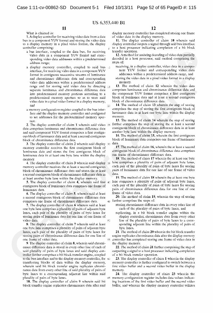
Case 1:11-cv-00862-SD Document 5-1 Filed 10/13/11 Page 52 of 65 PageID #: 115
US 6,353,440 Bl 11
What is claimed is: 1. A display controller for receiving video data from a data
bus in a component YUV format and storing the video data to a display memory in a pixel video format, the display controller comprising:
a bus interface, coupled to the data bus, for receiving video data in a component YUV format and corresponding video data addresses within a predetermined address range;
12 display memory controller has completed storing one frame of video data in the display memory.
11. The display controller of claim 10 wherein said display controller outputs a signal through said bus interface
5 to a host processor indicating completion of a bit block transfer operation.
12. Amethod for assisting decoding of video data partially decoded in a host processor, said method comprising the steps of:
a display memory controller, coupled to said bus 10
interface, for receiving video data in a component YUV format in contiguous successive streams of luminance and chrominance difference data and corresponding video data addresses within a predetermined address range and for storing said video data by directing 15
separate luminance and chrominance difference data into predetermined memory portions according to a predetermined memory aperture so as to store said video data in a pixel video format in a display memory; and 20
receiving, in a display controller, video data in a component YUV format and corresponding video data addresses within a predetermined address range, and
storing the video data in a pixel video format in a display memory.
13. The method of claim 12 wherein the video data comprises luminance and chrominance difference data and the component YUV format comprises a first contiguous block of luminance data and at least a second contiguous block of chrominance difference data.
14. The method of claim 13 wherein the step of storing comprises the step of storing the first contiguous block of luminance data in at least one byte lane within the display memory.
a memory configuration-register coupled to the bus interface and the display memory controller and configured to set addresses for the predetermined memory aperture.
2. The display controller of claim 1 wherein said video data comprises luminance and chrominance difference data and said component YUV format comprises a first contiguous block of luminance data and at least a second contiguous block of chrominance difference data.
3. The display controller of claim 2 wherein said display memory controller receives the first contiguous block of luminance data and stores the first contiguous block of luminance data in at least one byte lane within the display memory.
4. The display controller of claim 3 wherein said display memory controller receives the at least a second contiguous block of chrominance difference data and stores the at least a second contiguous block of chrominance difference data in at least another byte lane within the display memory.
15. The method of claim 14 wherein the step of storing 25 further comprises the step of storing the at least a second
contiguous block of chrominance difference data in at least another byte lane within the display memory.
16. The method of claim 15, wherein the first contiguous block of luminance data comprises one frame of luminance
30 data. 17. The method of claim 16, wherein the at least a second
contiguous block of chrominance difference data comprises one frame of chrominance difference data.
18. The method of claim 17 wherein the at least one byte 35 lane comprises a plurality of pairs of adj acent byte lanes,
each pair of the plurality of pairs of byte lanes for storing pairs of luminance data for one line of one frame of video data.
5. The display controller of claim 4, wherein said first 40
contiguous block of luminance data comprises one frame of luminance data.
19. The method of claim 18 wherein the at least one byte lane comprises a plurality of pairs of adj acent byte lanes, each pair of the plurality of pairs of byte lanes for storing pairs of chrominance difference data for one line of one frame of video data. 6. The display controller of claim 5, wherein said at least
a second contiguous block of chrominance difference data comprises one frame of chrominance difference data.
7. The display controller of claim 6 wherein said at least one byte lane comprises a plurality of pairs of adjacent byte lanes, each pair of the plurality of pairs of byte lanes for storing pairs of luminance data for one line of one frame of video data.
8. The display controller of claim 7 wherein said at least one byte lane comprises a plurality of pairs of adjacent byte lanes, each pair of the plurality of pairs of byte lanes for storing pairs of chrominance difference data for one line of one frame of video data.
9. The display controller of claim 8, wherein said chrominance difference data is stored in every other line of each of said plurality of pairs of byte lanes and said display controller further comprises a bit block transfer engine, coupled
20. The method of claim 19, wherein the step of storing 45 further comprises the steps of:
50
storing chrominance difference data in every other line of each of the plurality of pairs of byte lanes, and
replicating, in a bit block transfer engine within the display controller, chrominance data from every other line of the plurality of pairs of byte lanes to a corresponding adjacent line within the plurality of pairs of byte lanes.
21. The method of claim 20 wherein the bit block transfer engine replicates chrominance data after the display memory
55 controller has completed storing one frame of video data in the display memory.
22. The method of claim 21 further comprising the step of outputting a signal to a host processor indicating completion of a bit block transfer operation.
23. The display controller of claim 1 wherein the display memory controller is further configured to switch between a first video buffer and a second video buffer in the display memory.
to the bus interface and to the display memory controller, for 60
transferring blocks of data within the display memory, wherein said bit block transfer engine replicates chrominance data from every other line of said plurality of pairs of byte lanes to a corresponding adjacent line within said plurality of pairs of byte lanes.
24. The display controller of claim 23 wherein the 65 memory configuration register includes data values indicat
ing locations of the first video buffer and the second video buffer, and wherein the display memory controller utilizes
10. The display controller of claim 9 wherein said bit block transfer engine replicates chrominance data after said

Case 1:11-cv-00862-SD Document 5-1 Filed 10/13/11 Page 53 of 65 PageID #: 116
US 6,353,440 Bl 13
the data values to translate X and Y coordinate of a bit block transfer into memory addresses of the display memory.
25. The display controller of claim 24 wherein the data values in the memory configuration register are programmed from a central processing unit and, alternatively, the data 5
values are programmed from a basic input/output system read-only memory (BIOS ROM).
26. An electronically-readable medium storing a program for permitting a computer to perform a method of assisting decoding of video data partially decoded in a host processor, 10
the method comprising the steps of: receiving, in a desplay controller, video data in a com
ponent YUV format in contiguous successive streams of luminance and chrominance difference data and corresponding video data addresses within a pre deter- 15
mined address range,
setting addresses for a predetermined memory aperture by use of a memory configuration register, and
storing the video data by directing separate luminance and 20
chrominance difference data into predetermined memory portions according to the predetermined memory aperture so as to store said video data in a pixel video format in a display memory.
27. A display system for receiving video data from a data 25
bus in a component YUV format and storing the video data to a display memory in a pixel video format, comprising:
a data bus to supply video data in a component YUV format;
a display memory to store the video data in a pixel video 30
format;
14 a bus interface, coupled to the data bus, for receiving the
video data in a component YUV format and corresponding video data addresses within a predetermined address range;
a display memory controller, coupled to the bus interface, for receiving the video data in a component YUV format in contiguous successive streams of luminance and chrominance difference data and corresponding video data addresses within a predetermined address range and for storing said video data by directing separate luminance and chrominance difference data into predetermined memory portions according to a predetermined memory aperture so as to store the video data in a pixel video format in a display memory, the display memory controller storing Y data in consecutive odd byte locations on succeeding lines in the display memory by performing an address translation on the Y data, the display memory controller further storing U data in every fourth byte location starting with a second byte location and storing V data in every fourth byte location starting with a fourth byte location;
a memory configuration register coupled to the bus interface and the display memory controller and configured to set addresses for the predetermined memory aperture; and
a display to display the video data.
* * * * *

EXHIBIT 4
Case 1:11-cv-00862-SD Document 5-1 Filed 10/13/11 Page 54 of 65 PageID #: 117

Case 1:11-cv-00862-SD Document 5-1 Filed 10/13/11 Page 55 of 65 PageID #: 118
United States Patent [19]
Nally et ai.
[54] APPARATUS, SYSTEMS AND METHODS FOR CONTROLLING DATA OVERIAY IN MULTIMEDIA DATA PROCESSING AND DISPIAY SYSTEMS USING MASK TECHNIQUES
[75] Inventors: Robert Marshall Nally, McKinney; John C. Schafer, Wylie, both of Tex.
[73] Assignee: S3 Incorporated, Santa Clara, Calif.
[21] Appl. No.: 08/707,937
[22] Filed: Sep. 10, 1996
[51] Int. CI.6 ....................................................... G09G 5/36
[52] U.S. CI. .......................... 345/191; 345/501; 345/507; 345/113
[58] Field of Search ..................................... 345/418,302, 345/433, 434, 435, 112, 113, 114, 115,
118, 150, 152, 154, 328, 329-332, 340, 342, 501-503, 520, 521, 523, 524, 507, 188,509,51~ 191, 51~ 51~ 186,510
[56] References Cited
U.S. PATENT DOCUMENTS
5,257,348 10/1993 Roskowski et al. .................... 345/327
111111 1111111111111111111111111111111111111111111111111111111111111 US005977960A
[11] Patent Number:
[45] Date of Patent:
5,977,960 Nov. 2, 1999
5,398,309 3/1995 Atkins et al. ........................... 345/435
5,469,541 11/1995 Kingman et al. ....................... 345/509
5,506,604 4/1996 Nally et al. ............................. 345/154
5,590,254 12/1996 Lippincott et al. ..................... 345/435
5,604,514 2/1997 Hancock ................................. 345/154
Primary Examiner---U. Chauhan
Attorney, Agent, or Firm---Fenwick & West LLP
[57] ABSTRACT
A memory system 107,300 is provided which includes a
memory 107 having a data area for storing data words and
a mask area 302 for storing a control mask. Mask generation
circuitry 301 is provided for generating such a control mask
for storage in the mask area 302 of the memory 107. Mask controlled memory read control circuitry 303 is provided
which is operable to selectively retrieve from the mask area
302 bits of the mask stored therein and in response selec
tively retrieve and output data words stored in the data area
of the memory 107.
15 Claims, 4 Drawing Sheets
303 r---MASK-O-BJ-EcT-R-E-AD--I 209 '-<. 504 ---...... ADDRESS GENERATOR I
~ I I !-----Vo'W-1-----------r--+.,.----H DISPLAY POSITION CONTROLS I
I I
I
DISPLAY POSITION CONTROLS
IY COUNTI Ix COUNTI 516
~---------------------i VDW 2 I
I DISPLAY POSITION CONTROLS
i IY COUNT I Ix COUNTI I
IY COUNT I Ix COUNTI : I----==~~-II
I I
I
: (=) :
7----~9.!..----------- <--__ -.J ___ I-'
210 [soiVowl--] 209 ~ MEMORY MAPPER :
I I BASE ADDRESS I I
r-L!:::_ -===-_ =-==.!--i I 503 VDW 2 I I I J MEMORY MAPPER I
210 : I BASE ADDRESS I I L: ________ ~
• • I
507~
I 2 6 ···62
3 7 .. ·63 M L ___________ ---1
MASK READ I 0 REQUEST
MEMORY ADDRESS BUS
MASK READ I 0 GRANT
VOW 1 ACTIVE
MASK OBJECT FROM FRAME BUFFER 107
VIDEO READ I 0 REO
TO OVERALY SELECTOR
VIDEO READ I 0 GRANT

Case 1:11-cv-00862-SD Document 5-1 Filed 10/13/11 Page 56 of 65 PageID #: 119
u.s. Patent Nov. 2, 1999 Sheet 1 of 4 5,977,960
109
101
100\...
108
"""-
"-
./
PLAYBACK YIDEO
SOURCE
+ CPU
f SYSTEM MEMORY
LOCAL BUS
1&3
FRAME ...... BUFFER
(
107
FIC. 1
REAL-TIME YIDEO V 104
SOURCE
YGA. .-.. DISPLAY CONTROLLER !'-- 106 \
105
r-----------------------------l OBJECT 302~-----l 303( MASK GENERATED I I
I
I I I
MASK GENERATOR
I MASK I ! OBJECT !
107~ I L _____ ~
I
MEMORY READ I CONTROLS I
I 207 I
L 3
301 I / 60---------VIDE~-~:I~;_ --l I I
" I 202/205 ./ AND FIFO I
FI C.
PAINTING SCREEN IN YOW REGION
3
MEMORY DATA BUS
MEMORY READ CLOCK
FIC. 6
I • I
GRAPHICS PIPELINE I I
AND FIFO ! I
I I I
! I
I OYERLAY I
TO DAC 208
200 264/206 / SELECTOR I
~-----~
YIDEO PIPELINE
200
GRAPHICS MEMORY SCREEN REFRESH CONTROLS
605 D 606
PIXEL OUT
GRAPHICS PIPELINE I--I----I~~~
CRT PIXEL CLOCK I GRAPHICS I I FIFO 604 I L _________ .J

Case 1:11-cv-00862-S
D D
ocument 5-1 F
iled 10/13/11 Page 57 of 65 P
ageID #: 120
~ ______________________ rr-~:loru~~~~~----~;--~~~rnE~TED~EMO~ I . GENERATOR ~301 READ CONTROLS I ,
CPU DATA (GRAPHICS AND NON- • i ~I REAL-TIME
VIDEO)
200
VGA/GRAPHICS CONTROLLER
VIDEO PLAYBACK PIPELINE
201
I
---------- r--.J ! 208
I ,
- 206-l
GRAPHICS~204 I L----~LJ~I DISPLAY, ~ICOLOR LOOK I I I FIFO I UP TABLE ~.
Y ZOOMER
214
COLOR CONV
-MEMORY L _TO/FROM FRAME
SEQUENCER ~ BUFFER 107
X ZOOMER
215
FORMAT
, I • I , I
218
• I
I , ~300 , I , OVERLAY I
LC~NTR~t.....J
VIDEO ~ FIFO
205
FIG. 2
REAL-TIME VIDEO DATA
(V PORT)
I X ~ r '£1/ 212 213 I V II
SCALER L _____ ~ 21 : ____________ ~~~~~~Ej
d • rJl • ~ ~ ..... ~ = .....
z o ~ ~N
'""" \C \C \C
'JJ.
=-~ ~ ..... N 0 ....., ~
Ul .... \C ""-l ""-l .... \C 0\ =

Case 1:11-cv-00862-S
D D
ocument 5-1 F
iled 10/13/11 Page 58 of 65 P
ageID #: 121
303 ~
400 \
I BASE ADDRESS :
406---
4~1
I OFFSET START J 402 I
I-DEL X ~ X COUNTER
CLK .400 I
1-DEL Y r- Y COUNTER 403 '-t> 409
404 MASTER CONTROLSJ
I
FIG. 4
L x L Y 413 POS n POS t-i"<'
'--t> "--I>
4(1 4b M1
1 ~ 410 ABSOLUTE -640" ""v405 / ADDRESS -~4 ( +) _~ ADDRESS t---800" - M2 GATE t-
-1024- ----- " I -1- 1- M3
1 §~
=0 IF (X CNT =0) LOAD Y
- CONTROLS LOAD X
=0 IF (Y CNT =0) ,..-[> SAVE X
.!Q1 SAVE Y ,....
PIXEL POSITION PITCH SEL 0 MASK WRITE I/O GRANT
PITCH SEL 1 416, DATA J START '--- DATA GATE DATA OUT
DATA TYPE FORMATIER I RMW CYCLE /
MASK WRITE !LO REQUEST 415
d • rJl • ~ ~ ..... ~ = .....
z o ~ ~N
'""'" \C \C \C
'JJ.
=~ ~ ..... ~
o ...., ~
Ul .... \C ""-l ""-l .... \C 0\ =

Case 1:11-cv-00862-S
D D
ocument 5-1 F
iled 10/13/11 Page 59 of 65 P
ageID #: 122
303 ,--MASK-OMCrREAr)-1 209 ~ 504 --.... ADDRESS GENERATOR I
~-----ViiW-'------------l i IDiSPIAY POSITION CONTROLSI i , ,j ,I m , IY COUNTJlx CO\JNTI
DISPLAY POSITION CONTROLS
: I I Y COUNT I I X COUNT I I j
500
515 MEMORY MAPPER GRAPHICS MEMORY
BASE ADDRESS i
FIG. 5
MASK READ 1/0 REQUEST
~--------------------------------~ • VOW 2 IIIII ~( ~)~ II MEMORY ADDRESS BUS ! DISPLAY POSITION CONTROlS 517 .n.: t +) -r: I MASK READ I/O GRANT
! IY COUNT I Ix COUNTI (=)! t.= ___________ =.l VOWI ACTIVE
L 501 ..J ,.....---------------, MASK OBJECT 7----------------- -- ~ 64 BIT MASK REGISTER ~ FROM FRAME BUFFER 107 210 ________ VIDEO READ I 0 REQ
[502 VOW 1 ~ : 0 4 ••• 60 ., .. I 209 I MEMORY MAPPER • 1 5 ••• 61
! I BASE ADDRESS I ' 5071 ~56JvDw2----i
512
2 6···62
3 7·· • 63 TO OVERALY SELECTOR I ...---.:.......1-__ --,
J MEMORY MAPPER I 210 : I BASE ADDRESS L i ~ ________ :.J
VIDEO READ I/O GRANT
d • rJl • ~ ~ ..... ~ = .....
z o ~ ~N
'""'" \C \C \C
'JJ.
=~ ~ ..... ~
o ...., ~
Ul .... \C ""-l ""-l .... \C 0\ =

Case 1:11-cv-00862-SD Document 5-1 Filed 10/13/11 Page 60 of 65 PageID #: 123
5,977,960 1 2
Thus, due to the advantages of windowing, the need has arisen for efficient and cost effective windowing control circuitry. Such windowing circuitry should allow for the simultaneous processing of data received from multiple
APPARATUS, SYSTEMS AND METHODS FOR CONTROLLING DATA OVERLAY IN MULTIMEDIA DATA PROCESSING AND
DISPLAY SYSTEMS USING MASK TECHNIQUES
TECHNICAL FIELD OF THE INVENTION
5 sources and in multiple formats. In particular, such windowing control circuitry should be capable of efficiently and inexpensively controlling the occlusion and/or overlay of video and graphics data in a windowing environment. The present invention relates in general to multimedia
processing and display systems and in particular to apparatus, systems and methods for controlling data overlay 10
in multimedia processing and display systems using mask techniques.
SUMMARY OF THE INVENTION
BACKGROUND OF THE INVENTION
As multimedia information processing systems increase in popularity, system designers must consider new techniques for controlling the processing and display of data simultaneously generated by multiple sources. In particular, there has been substantial demand for processing systems which have the capability of concurrently displaying both video and graphics data on a single display screen. The development of such systems presents a number of design challenges, not only because the format differences between graphics and video data must be accounted for, but also because of end user driven requirements that these systems allow for flexible manipulation of the data on the display screen.
According to a first embodiment of the present invention, a memory system is provided which includes a memory having a data area for storing data words and a mask area for storing a control mask. The mask in this embodiment is an
15 occlusion mask. The mask will determine which pixels in the video window are graphics pixels (overlaid) and which are video pixels on a pixel-by-pixel basis. The control mask is an occlusion mask which determines which pixels in the video window are graphics pixels (overlaid) and which are
20 video pixels on a pixel-by-pixel basis. Mask generation circuitry is provided which generates a control mask for storage in the mask area of the memory. Mask controlled memory read control circuitry is provided which is operable to then selectively retrieve from the mask area bits of the
25 mask and in response selectively retrieve and output data words stored in the data area of the memory.
One particular technique for simultaneously displaying video and graphics data on a single display screen involves the generation of "windows." In this case, a stream of data 30
from a selected source is used to generate a display within a particular region or "window" of the display screen to the exclusion of any nonselected data streams defining a display or part of a display corresponding to the same region of the screen. The selected data stream generating the display 35
window "overlays" or "occludes" the data from the nonselected data streams which lie "behind" the displayed data. In one instance, the overall content and appearance of the display screen is defined by graphics data and one or more "video windows" generated by data from a video source 40
occlude a corresponding region of that graphics data. In other instances, a video display or window may be occluded or overlaid by graphics data or even another video window.
In the multimedia environment, the "windowing" described above yields substantial advantages. Among other 45
things, the user can typically change the size and location on the display screen of a given window to flexibly manipulate the content and appearance of the data being displayed. For example, in the case of combined graphics and video, the user can advantageously create custom composite visual 50
displays by combining multiple video and graphics data streams in a windowing environment.
Significantly, occluded video windows cannot be managed by software alone, as can occluded graphics windows. Special hardware windowing controls are required because 55
video data is constantly being updated whereas graphics data is updated (painted) only once.
In order to efficiently control windows in a multimedia environment, efficient frame buffer management is required. Specifically, a frame buffer control scheme must be devel- 60
oped which allows for the efficient storage and retrieval of multiple types of data, such as video data and graphics data. To be cost competitive as well as functionally efficient, such a scheme should minimize the number of memory devices and the amount of control circuitry required and should 65
insure that data flow to the display is subjected to minimal delay notwithstanding data type.
According to a second embodiment according to the principles of the present invention, an overlay control system is provided which includes a frame buffer for storing words of graphics and video data and an overlay control mask. Mask generation circuitry generates such a mask for storage in the frame buffer. Mask controlled overlay circuitry is provided which is operable in response to bits of the mask retrieved from the frame buffer to selectively retrieve and output words of the video data stream stored in the frame buffer.
According to a third embodiment of the present invention, a display system is provided which includes a display device for generating a display on a display screen and a frame buffer. Graphics data processing circuitry is further provided for processing a graphics data stream, the graphics data processing circuitry controlling the transfer of graphics data to and from a graphics memory area in the frame buffer. Mask generation control circuitry is included for generating a mask for storage in a mask object area of the frame buffer. Video data processing circuitry is provided for processing a video data stream and includes mask controlled circuitry operable in response to bits of the mask retrieved from the frame buffer to selectively retrieve words of the video data stream stored in the frame buffer. Finally, mask controlled output selection circuitry is provided for selecting for output to the display device in response to the bits of the mask between words of the graphics data retrieved from the frame buffer by the graphics processing circuitry and words of the video data retrieved from the frame buffer by the video processing circuitry.
The embodiments of the present invention provide significant advantages over the prior art. In particular, the principles of the present invention allow for efficient and cost-effective windowing a multimedia environment. Specifically, windowing control circuitry embodying the principles of the present invention provides for the efficient and inexpensive control of occlusion/overlay of video and graphics data in a windowing environment.
The foregoing has outlined rather broadly the features and technical advantages of the present invention in order that

Case 1:11-cv-00862-SD Document 5-1 Filed 10/13/11 Page 61 of 65 PageID #: 124
3 5,977,960
4 graphics and video data during processing prior to display on display unit 106. According to the principles of the present invention, VGA controller is operable in selected modes to store graphics and video data together in frame
the detailed description of the invention that follows may be better understood. Additional features and advantages of the invention will be described hereinafter which form the subject of the claims of the invention. It should be appreciated by those skilled in the art that the conception and the specific embodiment disclosed may be readily utilized as a basis for modifying or designing other structures for carrying out the same purposes of the present invention. It should also be realized by those skilled in the art that such equivalent constructions do not depart from the spirit and scope of the invention as set forth in the appended claims.
5 buffer 107 in their native formats. In a preferred embodiment, the frame buffer area is partitioned into video memory which generally includes those areas of the memory used for storing YUV formatted data, a graphics memory which generally includes those areas of the frame buffer
10 used for storing RGB formatted data, and a mask memory.
BRIEF DESCRIPTION OF THE DRAWINGS
For a more complete understanding of the present invention, and the advantages thereof, reference is now 15
made to the following descriptions taken in conjunction with the accompanying drawings, in which:
FIG. 1 is a high level functional block diagram of a processing and display system embodying the principles of 20
the present invention;
FIG. 2 is a detailed functional block diagram of the VGA controller depicted in FIG. 1;
In the preferred embodiment, display unit 106 is a conventional raster scan display device and frame buffer 107 is constructed from dynamic random access memory devices (DRAMs).
FIG.2 is a detailed functional block diagram emphasizing VGA controller 105 and the associated circuitry interfacing controller 105 with frame buffer 107 and display unit 106. The primary components of VGA controller 105 include a conventional VGNgraphics controller 200, a video playback pipeline 201 and a video pipeline 202. VGNgraphics controller 200 receives graphics data from CPU 101 and in conjunction with frame buffer 107 performs additional processing, for example color expansion, on that graphics data prior to delivery to the graphics display FIFO 204. FIG. 3 is a functional block diagram depicting a mask
controlled overlay control system according to the principles of the present invention;
FIG. 4 is a functional block diagram depicting in further detail the object mask generator of FIG. 3;
25 Video playback pipeline 201 interprets a file format containing video encoded into video data. Such pipelines are known in the art and are designed in response by the file format. Video pipeline 202, among other things, receives real-time video data from video source 107 and stores the
FIG. 5 is a functional block diagram depicting in further received video data in the video areas of the frame buffer detail the mask generated memory read controls of FIG. 3; 30
and
FIG. 6 is a functional block diagram depicting in further detail the overlay selector of FIG. 3.
memory. In addition, video pipeline 202 controls the retrieval from memory and passage through overlay controls 207 of the video data (either real-time or playback) to generate a "window" on the display screen. Video pipeline
DESCRIPTION OF THE PREFERRED EMBODIMENTS
35 202 is further operable to convert received YUV data (either from frame buffer 107 directly or video source 104) into RGB data and perform X and Y zooming on video data being sent to display 106. FIG. 1 is a high level functional block diagram of a
multimedia processing and display system 100 operable to process and simultaneously display both graphics and video 40
data according to the principles of the present invention. Display system 100 includes a central processing unit (CPU) 101 which controls the overall operation of system 100 and generates graphics data defining graphics images to be displayed. CPU 101 communicates with the remainder of 45
the system discussed below by a local bus 103. A real-time video source 104 is coupled to the VPORT of VGA controller 105 which provides digitized video data in real-time to be processed and displayed by system 100. Real-time video source 104 may be, for example, a real-time video data 50
source outputting video data in a YUV format. System 100 operates in conjunction with a system memory 108 which stores graphics and video data on a real-time basis. System memory 108 may be for example a random access memory (RAM), floppy disk, hard disk or other type of storage 55
device. A playback video (non-real-time) source 109 is provided coupled to CPU 109 via a local bus. Playback video source 109 maybe for example a MPEG decoder or other video source converting compressed data into a YUV
A memory sequencer 203 controls and arbitrates accesses to and from frame buffer 107 by VGNgraphics controller 200, video playback pipeline 201, and video pipeline 202. Graphics data output from VGNgraphics controller 200 is buffered and synchronized with the clocks controlling display 104 by a graphics first-in/first-out memory (FIFO) 204 while video data output from video pipeline 202 is buffered and synchronized with the clocks controlling display 104 by video first-in/first-out (FIFO 205). The graphics data stream output from graphics FIFO 204 may be used to either address a color look-up table 206, the output of which is provided to the inputs of an overlay selector 207, or may be passed directly to the inputs of overlay selector 207 as true color data. The inputs of overlay selector 207 also receive the video data stream output from video FIFO 205. The selected data output from overlay selector 207 is provided to the input of a digital analog converter (DAC) 208 which drives display monitor 106. The operation and control of overlay selector 207 will be discussed in further detail below.
Video pipeline 202 includes first video window control or RGB format.
A VGA controller 105 embodying the principles of the present invention is coupled to local bus 103. VGA control-
60 circuitry (VDWl) 209 and second video control circuitry (VDW2) 210 which control the transfer of video data from frame buffer 107 (via memory sequencer 203). In the preferred embodiment, video window control circuits 209 ler 105 will be discussed in detail below; however, VGA
controller 105 generally interfaces CPU 101 with real-time video source 104 and playback video source 109 with a 65
display unit 106 and a multi-format system frame buffer 107. Frame buffer memory 107 provides temporary storage of the
and 210 each are composed of a series of counters, registers and address generators which control the retrieval of data from the video areas of memory for generation of respective display windows. An x-scaler 211 is provided to compress

Case 1:11-cv-00862-SD Document 5-1 Filed 10/13/11 Page 62 of 65 PageID #: 125
5,977,960 5
incoming real-time YUV video data corresponding to a display line of pixels (i.e., along the x-axis of the display). X-scaler may for example use a truncation/error diffusion technique for data compression. A color converter 212 and formatter 213 are provided to convert video data, received either directly from x-scaler 211 or after storage and retrieval from frame buffer 107, from the native YUV format
6 rastering data out of frame buffer 107 to refresh the screen on display 106, and the pixel position of the raster data begins to match the pixel position of pixels in a "window of interest" as defined by VDWI or VDW2 on the screen, mask
5 generated read controls 303 are evoked. Mask generated memory read controls 303, using the mask in mask object 302 select which from area (i.e. video or graphics) in multi-format frame buffer 107 raster data will be retrieved. to an RGB format compatible with DAC 208. A y-zoomer
214 and an x-zoomer 215 are provided to expand RGB pixel data on a pixel-by-pixel basis along a given display row 10
(x-zooming) and/or on a display line by display line basis (i.e., y-zooming). Interconnection/multiplexing circuits 216-218 allow for the flexible processing of video data as will be discussed below. Video capture window control circuitry (VCW) 220 controls the transfer of incoming video 15
data, either in its original YUV form or following conversion
Mask generated memory controls of 303 also maintain a "data steering switch" FIFO (discussed below) that controls whether video data passing through a video pipeline 202 and video FIFO 205 or graphics data output from VGNgraphics controller 200 and graphics FIFO 204 is passed to a DAC 208. It should be noted that in the preferred embodiment, mask generated memory read controls 303 always attempt to keep video FIFO 205 full even when the display screen is
to an RGB format, to the frame buffer 107. In the preferred embodiment, video window control circuitry is constructed as a series of counters, registers, and address generators.
Interconnection/multiplexing circuits 216-218, along 20
with video window control circuitry 209 and 210 and video capture window control circuitry 220, advantageously allow for the flexible processing of incoming video data under the control of the system software being executed by CPU 101. For example, during video capture in an RGB format, 25
incoming YUV video data is first passed through x-scaler 211 for compression (as required), and then through color converter 212 and formatter 213 for conversion and reformatting into a selected RGB format. The RGB data is then, under the control of video capture window control circuitry 30
220, stored in frame buffer 107 as RGB data. In the illustrated embodiment, video display window controller (VDW2) 210 controls the subsequent retrieval of the RGB data from frame buffer 107 for delivery to display 106 while video display window controller (VDWl) 209 controls the 35
transfer of the RGB video data from the frame buffer 107 to
being refreshed in regions outside a "window of interest" (i.e., graphics data are being displayed) and during sync times. For purposes of the present discussion, a video window of interest is a region of pixels on the display screen where video data is intended to be displayed.
FIG. 4 is a more detailed functional block diagram of object mask generator 301. Object mask generator 301, under the direction of software being executed by CPU 101, defines the overlay control mask by flooding regions of masked object 302 with a defined one-bit value (either a logic one or a logic zero).
Object mask generator 301 includes a base address register 400, an offset start register 401, a DEL X register 402, a DEL Y register 403 and master controls register 404, each of which is loaded by CPU 101. Base address register 400 maintains a base address to the object mask 302 and offset start register 401 maintains an offset to the address of the starting position or pixel of a portion of the mask that is to be changed or modified. This selected portion of memory will be flood filled with new data. Master controls register
CPU 101 via local bus 103 for processing. Video data can also be captured in a YUV format. In this
case, the incoming video data stream is passed only through x-scaler 211 for compression (as required) and then sent directly to frame buffer 107 in its original YUV format. Video capture window control circuitry 220 controls the input of the video data stream and the subsequent storage of the data in frame buffer 107 after x-scaling. In the illustrated embodiment, video window control circuitry 209 (VDWl) is used during video capture in a YUV format to control data retrieval from frame buffer 107. Following retrieval from frame buffer 107, the YUV data is sent to color converter 212 and formatter 213 for conversion and formatting into RGB data and then on through y-zoomer 214 and x-zoomer 215 to overlay control circuitry 207. Video window controller 210 (VDW2) in this example controls the delivery of the converted data to CPU 101 via local bus 103 for further processing.
FIG. 3 is a high-level functional block diagram emphasizing mask controlled overlay circuitry 300 of system 100 constructed in accordance with the principles of the present invention. Mask controlled overlay circuitry 300 includes an object mask generator (OMG) 301, mask object 302 which is stored in frame buffer memory 107, mask generated memory read controls (MGMRC) 303 and overlay selector/ controls 207. Mask object 302 in the preferred embodiment comprises a selected space in frame buffer 107. Object mask generator 301 and mask generated memory read controls 303 will be described in detail below. In general, an overlay control mask is generated by object mask generator 301 and stored in mask object 302. When memory sequencer 203 is
404 holds a START bit, a DATA TYPE bit and PITCH SEL n bits. When the START bit is set to a logic one by CPU 101, a flood fill operation will begin in a selected region of the
40 mask object. The START bit field automatically clears to a logic zero when the flood fill is complete. The DATA TYPE bit determines what data value the selected portion of the mask object region will be flooded with. When a logic one is set into the DATA TYPE bit field, the region is corre-
45 spondingly filled with logic ones, when a logic zero is set in this bit field the region is filled with logic zeros. The PITCH SEL n bits (in the preferred embodiment there are two such bits) are used to determine the width in pixels of the mask object. In the illustrated embodiment, three resolutions are
50 provided for: 640; 800; and 1024 pixel-wide objects. As shown in FIG. 4, the PITCH SEL 0 and PITCH SEL 1 bits are used to toggle a multiplexer 405 which allows a corresponding mask size value to be passed from hard-wired registers 406. In the preferred embodiment, the offset start
55 register 401, DEL X register 402 and DEL Y register 403 are set up before the START bit is set. Base address register 400 and the PITCH SEL bits of master control register 404 are set up during VGA mode changes.
When the START bit is set to a logic one, the LOAD X 60 and LOAD Y outputs of control circuitry 407 are set high
which consequently loads the values in DEL X register 402 and DEL Y register 403 into X down counter 408 and Y down counter 409, respectively. With the first clock (CLK), the output of address gate 410 is set with an absolute address
65 of a 64-bit word in mask object area 302 of frame buffer 107 that contains the first pixel of the first line of a portion of the "window of interest" to be modified. The absolute address
Case 1:11-cv-00862-SD Document 5-1 Filed 10/13/11 Page 63 of 65 PageID #: 126
5,977,960 7
includes bits indicating the Pixel Position of that particular pixel within the addressed 64-bit word. Also, with the first clock, LOAD X and LOAD Y return to a low state. It should be noted that the address of the first pixel of the first line of the portion of the mask object that is being modified is the base address from base register 400 plus offset start from offset register 401, as controlled by selectors 413 and 414 in accordance with Table 1. The base address is equal to the selected display width from register 406 times a Y value, a X value, where the top left pixel of the video window is at pixel location (X,Y) as shown in FIG. 4. The absolute address output by address gate 410 is latched in corresponding X position register 411 and Y position register 412.
TABLE I
M1 M3 Addr Load Y Load X Selection Selection Generated
0 0 X Pas "1" Next pixel in current line
0 Y Pas M2 Output First pixel in new line
0 N/A N/A N/A Base Offset First pixel in Address Start first line
After the first clock, the value in X counter 408 equals the value in DEL X register 402 and the value in Y counter 409 equals the value in DEL Y register 403. X counter 408 decrements with each clock cycle thereafter until the value
8 counter 408 goes to zero (the trailing boundary is not 64-bit aligned) the internal flag is again set, indicating that the next mask right memory cycle will be a read-modify-write. In this case, the read-modify-write cycle occurs immediately.
5 Every time the contents of data formatter 415 are loaded into data gate 416, the entire 64-bits in data formatter 415 are reset to NOT DATA TYPE before the next clock cycle.
FIG. 5 is a more detailed functional block diagram of mask generated memory read controls 303. The primary
10 components of read controls 303 include the display position controls 500 of video window controls circuitry 209 and the display position controls 501 of video window control circuitry 210. Display position controls 500 and 501 include
15
20
25
counters and registers which define the regions on the display screen where video windows 1 and video windows 2 will be respectively displayed. The memory mapper 502 of video window 1 control circuitry 209 and the memory mapper 503 of video window 2 control circuitry 210 are used to maintain a base address to the frame buffer 107 address space in which the corresponding video data is being stored. Mask object read address generator 504 includes display position controls 505 and a memory mapper 506. Display position controls 505 include registers and counters which track the position of the current raster scan on the screen of display 106. Memory mapper 506 includes a register 515 which holds the base address to the mask object 302 address space in frame buffer 107. Mask generated memory read controls 303 also includes a 64-bit mask register 507, which will be discussed further below.
in X counter 408 equals zero. At the same time, a logic one 30
is added to the value in X position register 411 with each clock cycle. When X counter 408 decrements to zero, LOAD
When the X and Y counts in either video window 1 display position controls 500 or video window 2 display position controls 501 are equal to the X and Y counts in read address generator display position controls 505, as determined by respective comparison circuitry 516 and 517, the
X goes active (i.e. high) such that x-counter 408 reloads, the value in Y counter 409 decrements, and the address of the first pixel of the next line in the window is set into address gate 410 (i.e. the value held in Y position register 412 plus the output of selector 405) on the very next clock both x-position register 411 and y-position register 412 are updated with this new address and x-counter decrementing begins again. This process repeats until Y counter 409 decrements to zero at which time the operation terminates and START is reset to zero.
Object mask generator 301 also includes a data formatter 415 which in the preferred embodiment includes a 64-bit register. On each clock cycle the DATA TYPE value in the master controls register 404 is written to the bit position in data formatter 415 pointed to by the 6-bit Pixel Position value received from address gate 410. The Pixel Position value output from address gate 410 in the preferred embodiment is represented by the six LSBs of the absolute address. Data formatter 415 counts the number of Pixel Position bits (pixels) as they are loaded into its register and when it has collected 64 bits, generates a mask write I/O request to memory sequencer 203 and places the 64 bits as a data word in data gate 416. When memory sequencer 203 determines that frame buffer 107 is ready to receive this mask data a mask write I/O grant is sent back to data gate 416 and address gate 410 to release the current mask data and current absolute address to frame buffer 107.
Data formatter 415 also manages boundary conditions. For example, if the Pixel Position is not zero and LOAD X is active (the leading boundary is not 64-bit aligned), a flag
35 raster scan has reached a video window. In this case, a mask read I/O request is sent to memory sequencer 203 to initiate retrieval of mask bits from mask object 302. The X and Y counts from the active display window position control circuit 500 or 501 are then passed by selector 508 added to
40 the graphics memory base address in register 515 by adder 509 to obtain a memory address to mask object 302. The resulting address is sent to frame buffer 107 via the memory address bus when a mask read I/O grant is received from memory sequencer 203. It should be noted that the counters
45 in VDWI and VDW2 increment only when the outputs of their corresponding comparators 516 and 517 indicate an equal condition exists, while the counters in display position controls 505 are always counting with the raster scan.
Each address to mask object 302 results in the retrieval of 50 the corresponding 64 mask bits which are stored in mask
register 507. Each of the 64 bits are then stored in mask register 507. Four bits representing four pixels are next retrieved at a time from mask register 507 and compared by comparison circuitry 512 (four bits are compared at one time
55 because the width of the frame buffer data path in the preferred embodiment is 4 YUV pixels or 64 bits). If all four bits are a logic zero no video memory read cycle will take place (no video read I/O request is issued). If on the other hand, anyone of the four bits being compared is a logic one,
60 a video I/O request is sent to memory sequencer 203. When a Video Read I/O Grant is issued back from memory sequencer 203, a video memory read cycle starting at the address of the first pixel of the four will be generated by adder 510 and sent to frame buffer 107. That address is
is set internal to data formatter 415 indicating that the next mask right memory cycle will be a read-modify-write. When the Pixel Position equals 64 or when the value in X counter 65
408 equals zero, the read-modify-write cycle will occur. If the Pixel Position does not equal 64 when the value in X
generated using the active window memory mapper 502 or 503. The X and Y counts for the active video window are passed through multiplexer 508 to an adder 510 and added

Case 1:11-cv-00862-SD Document 5-1 Filed 10/13/11 Page 64 of 65 PageID #: 127
5,977,960 9
to the base address from the corresponding memory mapper 502 or 503 of the active video window as selected by a selector 511. The result is an address to the video memory in multi-format frame buffer 107 to retrieve the corresponding video data once a video read I/O grant has been issued 5
by memory sequencer 203. FIG. 6 is a detailed functional block diagram depicting the
interface between mask generated read controls 303, the graphics pipeline and FIFO 202/205 and graphics pipeline and graphics FIFO 202/204/206 with the overlay selector 10
207. As the mask bits are retrieved from register 507 to generate addresses for the memory read cycles, they are simultaneously sent to register 600 for overlay control. The current bit n in register 600 is compared by exclusive-OR gate 601 with the previous bit m being held in register 602. 15
If the state of the current bit n does not match the state of the previous bit m, a logic one is loaded into steering controls FIFO 603. The steering controls maintain a pixel train going to DAC 206. In the preferred embodiment pixel data is packed in frame buffer 107 for efficiency and therefore are 20
not necessarily in the proper order when they reach video FIFO 205 and graphics FIFO 204. The mask bits received into the steering controls determine which pixels will be placed in the video and graphics FIFOs 205 and 204. In the preferred embodiment, a non-displayed pixel will not be 25
loaded into either FIFO 204 or 205. It should be noted that one bit is placed in steering controls FIFO 603 (preferably a one-bit wide FIFO) for each pixel.
Each mask bit output from steering controls FIFO 303 drives AND gate 605 and flip-flop 606 to control whether 30
video data from video FIFO 205 is to be output to DAC 208
10 circuitry for generating a plurality addresses to storage
locations within said frame buffer, said locations for storing bits defining a selected region of said overlay control mask;
circuitry for generating mask data words of a selected logic value; and
circuitry for selectively presenting said addresses and said mask data words to said frame buffer such that said mask data words are written to said storage locations thereby defining said region of said overlay control mask.
3. The overlay control system of claim 2, wherein said circuitry for generating a plurality of addresses comprises:
an x-position counter for counting, in response to a clock, from an initial x-position value to a final x-position value;
a y-position counter for counting from an initial y-position value to a final y-position value when a count in said x-position counter reaches said final x-position value, said x-position counter resetting to said initial x-position value and continuing to count when a current count in said y-position counter has not reached said final y-position value;
an x-position register for storing a first portion of an address, to a first location in said frame buffer for storing a first bit of said region;
a y-position counter for storing a second portion of said address;
circuitry for modifying said first portion being stored in said x-position register with each change in count of said x-position counter; and
circuitry for modifying said second portion being stored in said y-position counter when said count in said x-position counter reaches said final value.
4. The overlay control system of claim 2, further comprising a data formatter having a plurality of storage locations each pointed to by selected bits of an address, said formatter accumulating for output as a data word a selected
or graphics data is to be output from graphics FIFO 204 to DAC 208. In the illustrated embodiment, the bits output from the steering controls register 603 and the CRT pixel clock are AND-ed together and the result used to toggle 35
flip-flop 606. The output of flip-flop 606 in turn drives the control input to overlay selector 207. As the overlay selector 207 toggles, data is retrieved from either the graphics FIFO 204 or video FIFO 205. 40 number of bits of said selected logic value in response to
said selected bits of corresponding ones of said addresses. 5. The overlay control system of claim 1, wherein said
mask controlled overlay selection circuitry comprises: display-position control circuitry for determining when a
position of a raster scan generating a display screen has reached a video window within said display screen;
circuitry for generating an address to said frame buffer to
Steering controls FIFO 603 includes a tap labeled in FIG. 6 "Two Graphics Memory Screen Refresh Controls." A steering control 604 includes a toggler similar to that shown in FIG. 6 which controls (605,606) requests for memory read cycles by the graphics screen refresh controls (not
45 shown). The tap is placed in the steering controls FIFO 603 at a point that ensures that the video pipeline 202/204/206 and the graphics pipeline 202/205 are aligned.
Although the preferred embodiment has been described in detail, it should be understood that various changes, substi - 50
tutions and alterations can be made therein without departing from the spirit and scope of the invention as defined by the appended claims.
What is claimed is: 1. An overlay control system comprising: a frame buffer for storing words of graphic data, words of
video data and an overlay control mask;
55
mask generation circuitry for generating said overlay control mask for storage in said frame buffer from a mask object, said mask object having fewer bits than 60
said overlay control mask; and
retrieve corresponding bits of said overlay control mask when said raster scan has reached said video window;
a register for storing said bits of said overlay control mask retrieved from said frame buffer;
circuitry for generating addresses to said frame buffer to retrieve words of said video data corresponding to said video window; and
an overlay selector for selectively outputting said words of said video data retrieved from said frame buffer in response to said bits of said overlay control mask stored in the register.
6. The overlay control system of claim 5 and further comprising comparison circuitry for comparing selected ones of said bits stored in said register to bits from displayposition control circuitry and generating, in response, a video read request signal to control circuitry associated with said frame buffer, said control circuitry providing in
mask controlled overlay selection circuitry operable in response to bits of said overlay control mask retrieved from said frame buffer to selectively retrieve and output words of said video data stored in said frame buffer.
2. The overlay control system of claim 1, wherein the mask generation circuitry further comprises:
65 response to said video read request signal, a video read grant signal to circuitry for generating addresses to enable the retrieval of said corresponding bits of said mask.

Case 1:11-cv-00862-SD Document 5-1 Filed 10/13/11 Page 65 of 65 PageID #: 128
5,977,960 11
7. A display system comprising:
a display device for generating a display on a display screen;
a frame buffer having a graphics memory area and a mask memory area;
graphics data processing circuitry for processing a graphics data stream, said graphics data processing circuitry controlling transfer of graphics data to and from the graphics memory area of said frame buffer;
mask generation circuitry for generating a mask for storage in the mask memory area of said frame buffer from a mask object, said mask object having fewer bits than said mask;
5
10
12 a y-position counter for storing a second portion of said
address;
circuitry for modifying said first portion being stored in said x-position register with each change in count of said x-position counter; and
circuitry for modifying said second portion being stored in said y-position counter when said count in said x-position counter reaches said final value.
10. The display system of claim 8, wherein said circuitry for generating mask data words comprises a data formatter having a plurality of storage locations each pointed to by selected bits of an address, said data formatter accumulating for output as a mask data word a selected number of bits of
video data processing circuitry for processing a video data stream including mask controlled circuitry operable in response to bits of said mask retrieved from said frame buffer to selectively retrieve words of said video data stream stored in said frame buffer; and
15 said selected logic value in response to at least some bits of corresponding ones of said addresses.
mask controlled output selection circuitry for selecting for 20
output to said display device in response to said bits of said mask between words of graphics data retrieved from said frame buffer by said graphics processing circuitry and words of said video data retrieved from said frame buffer by said video data processing cir- 25
cuitry. 8. The system of claim 7, wherein the mask generation
circuitry further comprises:
circuitry for generating a plurality of addresses to storage locations within a mask object storing bits, defining a 30
selected region of a mask;
circuitry for generating mask data words of a selected logic value; and circuitry for selectively presenting said addresses and said data words to said frame buffer such 35
that said mask data words are written to said storage locations in said mask object to define said selected region of said mask.
9. The display system of claim 8, wherein said circuitry for generating a plurality of addresses comprises:
an x-position counter for counting in response to a clock from an initial x-position value to a final x-position value;
40
11. The display system of claim 10, wherein said data formatter accumulates 64-bit mask data words for storage in said mask object.
12. The display system of claim 7, wherein said mask controlled circuitry of said video processing comprises:
display position control circuitry for determining when a position of a raster scan generating a said display screen on said display device has reached a video window within said display screen;
circuitry for generating an address to said frame buffer to retrieve bits of said mask from said mask object when said raster scan has reached said video window;
a register for storing said bits of said mask retrieved from said frame buffer;
circuitry for generating addresses to said frame buffer to retrieve words of said video data corresponding to said video window; and
comparison circuitry for comparing selected ones of said bits retrieved from said register to bits from displayposition control circuitry and generating in response a video read request to control circuitry associated with said frame buffer, said control circuitry providing in response to said read request a video read grant to circuitry for generating addresses to enable the retrieval of said video data corresponding to said video window.
13. The display system of claim 12, wherein said mask a y-position counter for counting from a initial y-position
value to a final y-position value when a count in said x-position counter reaches said final x-position value, said x-position counter resetting to said initial x-position value and continuing to count when a current count in said y-position counter has not reached said final y-position value;
controlled output selection circuitry received said bits of 45 said mack from said register an performs an output selection
in response thereto.
an x-position register for storing a first portion of an address to a first location in said frame buffer for storing a first bit of said region;
50
14. The display system of claim 12, wherein said register stores mask bits as 64-bit blocks received from said mask object.
15. The display system of claim 12, wherein said comparison circuitry compares 4 said selected bits at a time.
* * * * *