Finite size and intrinsic field effect on the polar-active ... · To be submitted to Phys. Rev. B...
35
To be submitted to Phys. Rev. B Finite size and intrinsic field effect on the polar-active properties of the ferroelectric- semiconductor heterostructures A.N. Morozovska 1* , E.A. Eliseev 1,2 , S.V. Svechnikov 1 , V.Y. Shur 3 , A.Y. Borisevich 4 , P. Maksymovych 4 , and S.V. Kalinin 4† , 1 Institute of Semiconductor Physics, National Academy of Sciences of Ukraine, 03028, Kiev, Ukraine 2 Institute for Problems of Materials Science, National Academy of Sciences of Ukraine, 03142, Kiev, Ukraine 3 Institute of Physics and Applied Mathematics, Ural State University, 620083, Ekaterinburg, Russia 4 Oak Ridge National Laboratory, 37831, Oak Ridge, Tennessee, USA Abstract Using Landau-Ginzburg-Devonshire approach we calculated the equilibrium distributions of electric field, polarization and space charge in the ferroelectric-semiconductor heterostructures containing proper or incipient ferroelectric thin films. The role of the polarization gradient and intrinsic surface energy, interface dipoles and free charges on polarization dynamics are specifically explored. The intrinsic field effects, which originated at the ferroelectric- semiconductor interface, lead to the surface band bending and result into the formation of depletion space-charge layer near the semiconductor surface. During the local polarization reversal (caused by the inhomogeneous electric field induced by the nanosized tip of the Scanning Probe Microscope (SPM) probe) the thickness and charge of the interface layer * [email protected] † [email protected] 1
Transcript of Finite size and intrinsic field effect on the polar-active ... · To be submitted to Phys. Rev. B...
To be submitted to Phys. Rev. B
Finite size and intrinsic field effect on the polar-active properties of the ferroelectric-
semiconductor heterostructures
A.N. Morozovska1*, E.A. Eliseev1,2, S.V. Svechnikov1, V.Y. Shur3, A.Y. Borisevich4,
P. Maksymovych4, and S.V. Kalinin4†,
1Institute of Semiconductor Physics, National Academy of Sciences of Ukraine,
03028, Kiev, Ukraine
2Institute for Problems of Materials Science, National Academy of Sciences of Ukraine,
03142, Kiev, Ukraine
3Institute of Physics and Applied Mathematics, Ural State University,
620083, Ekaterinburg, Russia
4Oak Ridge National Laboratory, 37831, Oak Ridge, Tennessee, USA
Abstract
Using Landau-Ginzburg-Devonshire approach we calculated the equilibrium distributions
of electric field, polarization and space charge in the ferroelectric-semiconductor heterostructures
containing proper or incipient ferroelectric thin films. The role of the polarization gradient and
intrinsic surface energy, interface dipoles and free charges on polarization dynamics are
specifically explored. The intrinsic field effects, which originated at the ferroelectric-
semiconductor interface, lead to the surface band bending and result into the formation of
depletion space-charge layer near the semiconductor surface. During the local polarization
reversal (caused by the inhomogeneous electric field induced by the nanosized tip of the
Scanning Probe Microscope (SPM) probe) the thickness and charge of the interface layer
* [email protected] † [email protected]
1
drastically changes, it particular the sign of the screening carriers is determined by the
polarization direction. Obtained analytical solutions could be extended to analyze polarization-
mediated electronic transport.
1. Introduction
Polar discontinuity at the interfaces induced either by translational symmetry breaking of a
ferroelectric material or ionic charge mismatch between component can produce intriguing
modification of the of the interfacial electronic states and polarization of the adjacent materials
[1, 2, 3, 4]. The representative interfacial phenomena arising from the interplay between polarity
and electronic structure include two-dimensional electron gases at the interface of band
(LaAlO3/SrTiO3) [2] or band and Mott insulators [5] and polarization-controlled electron
tunneling across ferroelectric-semiconductor or bad-metal interfaces (PbTiO3/(La,Sr)MnO3,
BaTiO3/SrRuO3). [6, 7, 8, 9] These novel physical phenomena emerging in oxide materials at the
nanometer scale hold strong potential for novel devices. Correspondingly, the theoretical insight
into the epitaxial interfaces of normal and incipient ferroelectrics with bad metals and
semiconductors and interplay between atomistic phenomena at interfaces and mesoscopic
potential and field distributions is acutely needed.
As an illustrative example, the notorious problem of the Schottky barrier in ferroelectric
films is still widely debated, with the key question of whether sub-100 nm films are fully
depleted, or that the width of the depletion regions is in the sub-10 nm range due to the overall
high density >1020 cm-3 of shallow and deep donor and/or acceptor levels in the film, and
particularly in the interfacial regions. [10] More importantly, only several previous works, such
as the concept of a ferroelectric Schottky diode [11] and the dielectric non-linearities in the
epitaxial PZT films [12, 13], have emphasized the effect of space-charge layers on polarization
distribution and domain switching dynamics inside ferroelectric films.
In the current paper we present analytical calculations of the polar-active properties
(including local polarization reversal) in the proper and incipient ferroelectric-dielectric thin films
within Landau-Ginzburg-Devonshire phenomenological approach, with a special attention to the
polarization gradient and intrinsic surface energy, interface dipoles and free charges. We
analyzed the influence of finite size effect on the intrinsic electric field and polar-active
properties of the ferroelectric-semiconductor heterostructures. Although the stability of the
2
spontaneous polarization in the system ferroelectric film /insulator/semiconductor was previously
studied within LGD approach [14], the band structure of the system, interface charges and
dipoles, the polarization gradient and intrinsic surface energy of ferroelectric film were
previously ignored. Hence, this work provides a framework to link the mesoscopic LGD-
semiconductor theory to the first–principle calculations that can reveal the electrostatic details of
the interface structure.
The paper is organized as follows. After stating the problem in Section 2, analytical
solutions for polarization, electric potential, field and space charge distributions in the model
heterostructure are presented in the Section 3.1. The results of the stable ground state calculations
for SrTiO3/(La,Sr)MnO3 (STO/LSMO) and BiFeO3/(La,Sr)MnO3 (BFO/LSMO) heterostructures
are presented Section 3.2. Metastable states are considered in Section 3.3. The effect of the
incomplete screening and interface charge on the local polarization reversal and domain
formation caused by the electric field of the SPM tip is studied in Section 4. The tunneling
current density is estimated, providing an analytical approach to quantify recent experimental
measurements of polarization-controlled tunneling [6,7,8,9].
2. The problem statement
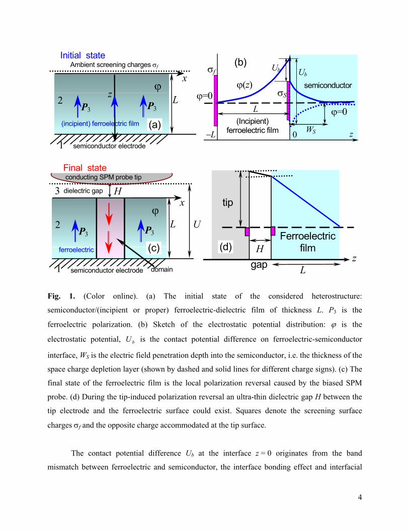
Here we consider an asymmetric heterostructure consisting of a narrow-gap (or metallic)
semiconductor and a thin ferroelectric film of thickness L. We will consider the two cases of the
proper and incipient ferroelectric films, both either a wide-gap semiconductor or a dielectric (i.e.
semiconducting properties of ferroelectric are neglected). In the initial state, the external bias is
absent and the free ferroelectric surface z = −L is completely screened by the ambient sluggish
charges [Fig. 1a]. Then inhomogeneous external bias U(x,y) is applied to the tip electrode. The
bias increase may cause local polarization reversal below the tip that finally results into
cylindrical domain formation in thin ferroelectric film [see the final state in Fig. 1c]. Note that
while we consider the tip-induced polarization switching, the obtained solutions are applicable
for capacitor geometry in the limit of uniform potential.
3
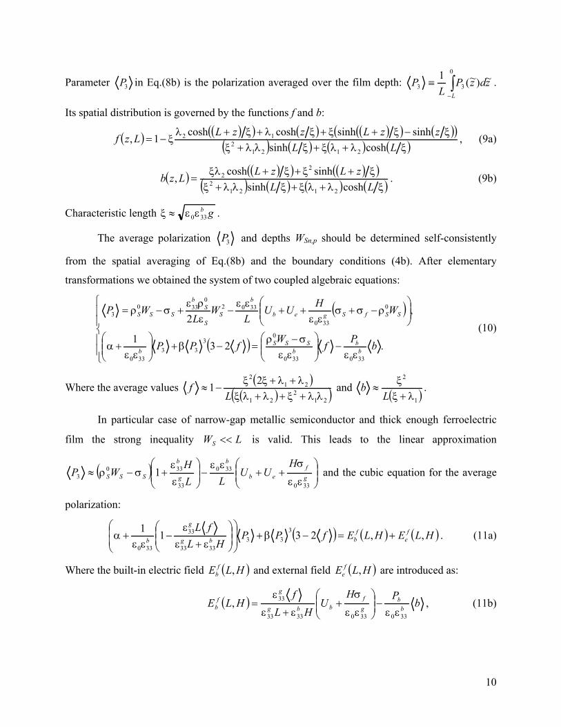
L
ϕ(z)
WS 0 z(Incipient)
ferroelectric film
semiconductor
Ub
−L
ϕ=0 ϕ=0
Ub σf
σS
1
L P3 P3
x ϕ
semiconductor electrode
2
H
L z P3 P3
x
ferroelectric
ϕ
semiconductor electrode
conducting SPM probe tip
U
dielectric gap 3
2
domain 1
(incipient) ferroelectric film
Initial state Ambient screening charges σf
z
(a)
(b)
(c) Hz
tip
Ferroelectric film
gap L
(d)
Final state
Fig. 1. (Color online). (a) The initial state of the considered heterostructure:
semiconductor/(incipient or proper) ferroelectric-dielectric film of thickness L. P3 is the
ferroelectric polarization. (b) Sketch of the electrostatic potential distribution: ϕ is the
electrostatic potential, U is the contact potential difference on ferroelectric-semiconductor
interface, W
b
S is the electric field penetration depth into the semiconductor, i.e. the thickness of the
space charge depletion layer (shown by dashed and solid lines for different charge signs). (c) The
final state of the ferroelectric film is the local polarization reversal caused by the biased SPM
probe. (d) During the tip-induced polarization reversal an ultra-thin dielectric gap H between the
tip electrode and the ferroelectric surface could exist. Squares denote the screening surface
charges σf and the opposite charge accommodated at the tip surface.
The contact potential difference Ub at the interface z = 0 originates from the band
mismatch between ferroelectric and semiconductor, the interface bonding effect and interfacial
4
polarity [Fig. 1b]. The band bending (or intrinsic field effect) in the semiconductor leads to the
depletion (or accumulation) charged layers of thickness WS with space charge ρS.
The screening interface charge σS could originate at z = 0 self-consistently in the case of
the bad screening from the semiconductor side (i.e. for thick depletion layer created by the minor-
type carriers). The non-ideal screening that causes the strong depolarization field controls the
self-consistent mechanism. The field decreases the polarization inside the ferroelectric film and
increases the free energy of the system, since depolarization field energy is always positive. As a
result, the strong field effect may lead to the bend bending at z = 0 and appearance of charge
states at the interface. The interface charges σS of appropriate sign provide effective screening of
the spontaneous polarization, make it more homogeneous and thus decrease the depolarization
field, which in turn self-consistently decreases the system free energy. The density of the
interface charge σS depends on energetic position of chemical potential µ at the surface that
modifies the Shottky barrier. The potential µ is manly determined by the interface layers with the
energy density NS (per unit energy) of quasi-continuous surface states and Fermi level EF at the
neutral surface [15, 16, 17].
We assume that in the initial state the sluggish surface charges σf completely screen the
electric displacement outside the film, i.e. ),,(),,( 3 LyxDLyxf −−=−σ , ( ) 0,, =−ϕ Lyx and
. This behavior is analyzed in Section 3. In contrast, recharging of the surface
charges σ
0)(3 =−< LzD
f should appear during the polarization reversal. The ultra-thin dielectric gap of
thickness H models the resistive properties of the sluggish surface charges σf, contamination or
dead layer. Corresponding free image charges −σf are accommodated at the conducting SPM tip
surface. Without loss of generality one can assume that the equilibrium domain structure is
almost cylindrical for the case of complete local polarization reversal in thin ferroelectric film.
The assumptions significantly simplify the problem considered in the Section 4, and allows
developing the analytical description for the domain formation.
Hereinafter we assume that the time of external field changing is small enough for the
validity of the quasi-static approximation 0≈Erot . Maxwell's equations for the quasi-static
electric field E and displacement D inside semiconductors have the form: ϕ−∇=
( ) )(0 ϕρ=+ε= PED divdiv . (1)
5

Here the electrostatic potential ϕ(x,y,z) is determined by external bias as well as by contact and
surface effects. The potential determines the free carrier density )(ϕρ determined by the
concentration of holes in the valence band, electrons in the conduction band, and acceptors and
donors at their respective levels in the band gap [16].
The ferroelectric film that occupies the region 0<<− zL is transversally isotropic, i.e.
permittivity ε11 = ε22 at zero electric field. We further assume that the dependence of in-plane
polarization components on can be linearized as 2,1E ( ) 2,11 E1102,1P −εε≈ ( ε is the universal
dielectric constant), while the polarization component nonlinearly depends on external field.
Thus corresponding polarization vector acquires the form:
0
3P
( ) ( ) ( ) ( ) ( )( )3E33031101110 1,,,1 PE b −εε+−εε−εε= rErP 21 E [18].
Within the framework of the Landau-Ginzburg-Devonshire (LGD) theory, quasi-
equilibrium polarization distribution P3(x,y,z) in the ferroelectric film with the spatial dispersion
should be found from the Euler-Lagrange boundary problem:
=−=
∂∂
λ−−==
∂∂
λ+
∂ϕ∂
−=
∂∂
+∆−β+α ⊥
.0,0
,
323
313
32
23
33
LzzP
PPzz
PP
zP
zgPP
b
(2)
Hereinafter we introduced a transverse Laplace operator 2
2
2
2
yx ∂∂
+∂∂
=∆⊥ .
The temperature-dependent coefficient α is positive for incipient ferroelectric and proper
ferroelectrics in paraelectric phase, while α<0 for proper ferroelectrics in ferroelectric phase,
β > 0 for the second order ferroelectrics considered hereinafter, gradient coefficient g > 0.
Extrapolation lengths λ1,2 originate from the surface energy coefficients in the LGD-free energy.
Inhomogeneity Pb describes the effect of the interface polarization stemming from the
interface bonding effect and associated interface dipole [19, 20]. More generally, the translation
symmetry breaking inevitably present in the vicinity of the any interface will give rise to
inhomogeneity in the boundary conditions (2) [21, 22].
Eqs. (1)-(2) yield the coupled system:
6

.0),(
,0,)(1
,,0
2
2
0
3
0112
2
33
2
2
>ϕρ−=
ϕ∆+
∂ϕ∂
εε
<<−
ϕρ−
∂∂
ε=ϕ∆ε+
∂ϕ∂
ε
−<<−−=
ϕ∆+
∂ϕ∂
⊥
⊥
⊥
zz
zLz
Pz
LzLHz
SS
fb (3)
The background dielectric permittivity of (incipient) ferroelectric ε (typically ε ); b33
b3333 ε>> Sε is
the semiconductor (bare) lattice permittivity.
Eqs.(3) are supplemented with the boundary conditions at z = −L−H, z = −L, z = 0 and
z = +∞, namely
( ) ),(,, yxUHLyx e=−−ϕ , ( ) ( )0,,0,, −−ϕ=+−ϕ LyxLyx , ( ) 0,, =∞→ϕ zyx , (4a)
( ) ( ) bUyxyx =−ϕ−+ϕ 0,,0,, , (4b)
),()0,,(
)0,,()0,,(
03330 yxzyx
yxPzyx
SSb σ=
∂+ϕ∂
εε−−−∂
−ϕ∂εε , (4c)
),()0,,()0,,()0,,(0333330 yx
zLyxLyxP
zLyx
fgb σ=
∂−−ϕ∂
εε++−+∂
+−ϕ∂εε− . (4d)
Where Ub is the contact potential difference at the dielectric-semiconductor interface. is the
dielectric constant of the dielectric gap between the tip and ferroelectric surface. The potential
distribution produced by the SPM tip is assumed to be almost constant in the surface
spatial region much larger then the film thickness.
g33ε
),( yxU e
3. Solution for polarization, electric potential, field and space charge distributions
3.1. Analytical solutions for the one-dimensional case
Here we calculate the potential and polarization distribution in the initial ground state in
the one-dimensional case Ue = const that corresponds to the plain electrodes. The case is realized
in paraelectric or incipient ferroelectric film as well as in the monodomain state of the proper
ferroelectric thin film.
The space charge density inside the doped p-type (or n-type) semi-infinite semiconductor
has the form
7
( ) ( ) ( ) ( )( )( ) ( )
( ) ( ) .,
,,
,)(
0
0
ϕ−−⋅=ϕ
ϕ−−⋅=ϕ
ϕ+−⋅=ϕ
ϕ+−⋅=ϕ
ϕ−ϕ−ϕ+ϕ=ϕρ
−
+
−+
TkqEEFNN
TkqEEFNn
TkqEEFNN
TkqEEFNp
NnNpq
B
Faaa
B
FCe
B
dFdd
B
VFp
adS
(5)
Where is the Fermi-Dirac distribution function, q is the absolute value of the
carrier elementary charge. E
( ) ( )( 11exp −+θ=θF
ρS
( )
)
F, EV, EC, Ed and Ea are the energies of Fermi level, valence band,
conductance band, donor and acceptor levels in the quasi-neutral region of the semiconductor
correspondingly. Since in the quasi-neutral region of the semiconductor, where
, the identity
0)( →ϕ
( )0→ϕ ( ) ( ) 000 =− −aNn
constNa ≈−
EE VF
0 −+dN
const
0 +p
Nd ≈+
Tkq BF >>ϕ−
should be valid. The identity along with
typical assumption , and Boltzman approximation for electrons
or holes EEC − Tkq B>>ϕ+− lead to expressions
−
ϕ− 1exp0
Tkq
BS≈ρ qpS or
−1
ϕ− exp0
Tkq
qnB
S≈ρS correspondingly, where and are
equilibrium concentrations of holes and electrons in the quasi-neutral region of the
semiconductor [23].
0Sp 0
Sn
Then in depletion layer (or abrupt junction) approximation the space charge density near
the interface of the strongly doped p-type (or n-type) semi-infinite semiconductor has the form
>
<<ρ≈ϕρ
S
SSS Wz
Wz
,0
0,)(
0
(5b)
Hereinafter the choice of the charge density ρ and depth W00SS qp= SpS W= (or ρ and
) is determined by the sign of potential (i.e. by the sign of charge in depletion layer).
More rigorously, for the definite type of carriers the thicknesses of the depletion layers W
00SS qn−=
SnS WW =
S (i.e.
the field penetration depths) should be determined self-consistently from the exact solution of the
system (3)-(5).
The ferroelectric film is regarded as a wide-gap proper semiconductor or almost
dielectric, so its space-charge density is negligibly small: 0)( ≈ϕρ f at 0<<− zL . The nonzero
1D-solution of Eqs. (3) with respect to the boundary conditions (4a) and (4c-e) is
8
( ) ( )
( ) ( )
( )
−<≤−−ρ−σ+σεε++
+
<≤−ρ−σ+σεε
++
εεσ−ρ
+−εε
>−θ−εε
ρ−
≈ϕ ∫−
.,
,0,~)~(
,0,2
)(
0
330
0
330330
0
330
3
2
0
0
LzHLWzLH
U
zLWH
UW
zLzdzP
zzWzW
z
SSfSge
SSfSgebSSS
z
Lb
SSS
S
(6)
Here θ(z) is the step-function. So the semiconductor potential and space charge are distributed in
the layer and zero outside. Approximate expressions (6) for the potential ϕ
correspond to parabolic approximation valid in the depletion/accumulation limit, at that
or W depending of the main carriers n or p-type. Note, that in the
accumulation regime the interface charge σ
SWz <<0
Sn >>SpSn WW << SpW
S is localized in the thin depletion layer of several nm
(for oxide electrodes) thickness WS that is occupied by the main-type carriers. The opposite case
of charged layers created by the minor-type carriers, which can appear during the polarization
reversal, could lead the strong band bending and accommodation of σS.
From Eq.(6) we derived the electric field E3 and electrical displacement D3 distributions
in the parabolic approximation:
( ) ( ) ( ) ( ) .0at,)(,)(
,0at,)(,)()(
03
0
0
3
03
330
0
330
33
>−θ−ρ=−θ−εερ
≈
<<−σ−ρ=εε
σ−ρ+
εε−≈
zzWWzzDzWWzzE
zLWzDWzPzE
SSSSSS
S
SSSbSSS
b
(7)
Note, that the free screening charge )(3 LDf −=σ− should also originate at another interface
z = −L. Thus the condition for electroneutrality of the whole system is . 00 =σ+ρ+σ− fSSS W
Allowing for Eqs.(6)-(7) polarization distribution P3(z) was found from the Euler-
Lagrange boundary problem (2) as described in Appendix A. The polarization distribution
acquires the form:
( ) ( ) 0,1)( 03 ≥−θ⋅−ρ
ε−ε
= zzWWzzP SSSS
S , (8a)
( ) ( ) 0),,(,13
2)(
23330
033330
3 ≤<−⋅−+β+αεε
σ−ρ+βεε= zLLzbPLzf
P
WPzP b
b
SSSb
. (8b)
9
Parameter 3P in Eq.(8b) is the polarization averaged over the film depth: ∫−
≡0
33~)~(
1
L
zdzPL
P .
Its spatial distribution is governed by the functions f and b:
( ) ( )( ) ( ) ( )( ) ( )( )( ) ( ) ( ) ( )ξλ+λξ+ξλλ+ξ
ξ−ξ+ξ+ξλ+ξ+λξ−=
LLzzLzzLLzf
coshsinhsinhsinhcoshcosh1,
21212
12 , (9a)
( ) ( )( ) ( )( )( ) ( ) ( ) ( )ξλ+λξ+ξλλ+ξ
ξ+ξ+ξ+ξλ=
LLzLzLLzb
coshsinhsinhcosh,
21212
22 . (9b)
Characteristic length gb330εε≈ξ .
The average polarization 3P and depths WSn,p should be determined self-consistently
from the spatial averaging of Eq.(8b) and the boundary conditions (4b). After elementary
transformations we obtained the system of two coupled algebraic equations:
( )
( )
εε−
εε
σ−ρ=−β+
εε
+α
ρ−σ+σ
εε++
εε−
ερε
+σ−ρ=
.231
,2
330330
03
33330
0
330
33020
3303
bPfWfPP
WHUUL
WL
WP
bb
bSSS
b
SSfSgeb
b
SS
Sb
SSS
(10)
Where the average values ( )( )( )21
221
212 21
λλ+ξ+λ+λξλ+λ+ξξ
−≈L
f and ( )1
2
λ+ξξ
≈L
b .
In particular case of narrow-gap metallic semiconductor and thick enough ferroelectric
film the strong inequality W is valid. This leads to the linear approximation LS <<
( )
εε
σ++
εε
+σ−ρ≈ gf
ebg
b
SSS
HU
LH
WP33033
3303 1
εε−
b
UL
330 and the cubic equation for the average
polarization:
( ) ( ) ( HLEHLEfPPHL
fL fe
fbbg
g
b ,,2311 333
3333
33
330
+=−β+
ε+εε
−εε
+α )
)
. (11a)
Where the built-in electric field and external field ( HLE fb , ( )HLE f
e , are introduced as:
( ) bPH
UHL
fHLE b
bgf
bbg
gf
b3303303333
33,εε
−
εε
σ+
ε+ε
ε= , (11b)
10
( )HL
UfHLE bg
eg
fe
3333
33,ε+ε
ε= . (11c)
Note that Eq.(11a) this is equivalent to the equation for ferroelectric polarization
hysteresis loop in the uniform electric field, while the built-in field determines the
horizontal imprint of the loop. Thus for the case considered by Eqs.(11) the symmetric intrinsic
coercive fields
( HLE fb , )
βα
−±=3
332b
cE of a bulk material [24] become asymmetric and has the form.
( ) ( ) ( ) ( )3
3333
33
330
11231
332,,,
ε+εε
−εε
+α−β
−±−=±
HLfL
Tf
HLETHLE bg
g
bf
bc . (12)
Renormalization of the coefficient α in Eq.(11), i.e. the term
ε+ε
ε−
εε HLfLbg
g
b3333
33
330
11
,
quantitatively reflects the “extrinsic contribution” (factor 103333
33 <ε+ε
ε<
HLL
bg
g
) originated from
the depolarization field produced by the finite gap H and the “intrinsic contribution” (factor
10 ≤< f ) originated from the finite extrapolation lengths λi < ∞ and intrinsic polarization
gradient ( 1=f for either g=0 or both λi = ∞). Thus Eq.(11) allows rigorous estimations of both
extrinsic and intrinsic contributions into the renormalization of the transition temperature into
paraelectric phase (compare the result with Ref.[25]).
For proper ferroelectrics the coefficient ( )*)( cT TTT −α=α , where T is the absolute
temperature and T is the Curie temperature possibly renormalized by misfit strain originated
from the film and semiconductor substrate lattice mismatch. For instance,
*c
11
1112* 2c
qcquTT
T
mcc
−α
+= 1112c , where um is a misfit strain, the stiffness tensor cijkl is positively
defined, qijkl stands for the electrostriction stress tensor.
Hence, the critical thickness (as well as the critical temperature) of the size-induced
transition of the ferroelectric film into paraelectric phase can be found from the condition
011
3333
33
330
=
ε+εε
−εε
+αHL
fLbg
g
b as:
11

( )( )
( )( )
ε+
λλ+ξ+λ+λξελ+λ+ξξ
αε−≈
gbcrH
TTL
33212
2133
212
0
21)( , (13)
( ) ( )( )( )
λλ+ξ+λ+λξλ+λ+ξξ
−ε+ε
ε−
εεα−≈
212
21
212
3333
33
330
* 2111LHL
LTLT bg
g
bT
ccr . (14)
For unstrained incipient ferroelectric film the coefficient α(T) is positive up to zero
temperatures and typically is given by Barret’s formula, thus the critical temperature (as well as
the critical thickness) does not exist, since the film remained paraelectric up to zero Kelvin.
However for the strained film it may become positive, indicative of the transition to the
ferroelectric state [26].
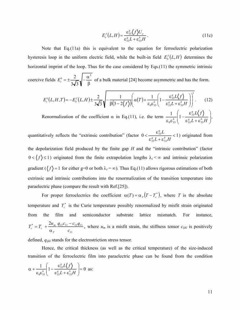
For particular case H = 0 (gap is absent) the build-in field Ebf is inversely proportional to
the film thickness, ( ) LBLE fb ≈0, , while its value depends on the built-in polarization Pb,
surface charge σf, and contact potential difference Ub [see Eq.(11b) and the dashed almost
straight line in Fig. 2a]. The build-in field Ebf leads to the vertical asymmetry and horizontal
imprint of the polarization hysteresis loops in ferroelectric films of thickness more than critical
[see regions 2 and 3 in Fig.2a and Fig. 2b]. Field-induced polarized state appears at
film thickness less than the critical one
)(TLL cr>
)(TLL cr< [see regions 5 and 6 in Fig.2a and Fig. 2c].
For typical ferroelectric material parameters approximate expressions for the right and left
coercive biases are ( ) ( ) ( ) ( )( )31,0, LTLTELBTLE crbcc −±−≈± [see Eq.(12)]. Thus solid
curves in Fig. 2a look like an asymmetric “bird beak” with the tip ( ) ( crcrc LBLLE −≈=± )
( )
and
asymptotes . The built-in field sign and thickness dependence determine
the beak «up» or «down» asymmetry and shape correspondingly.
( ) TELLE bccrc ±→>>±
12

0.2 0.4 0.6 0.8 1
-1.5
-1
-0.5
+0.5
+1
1.5
0
Up state is stable Down state is metastable
Eef/Ec
b
Right coercive field Ec+
Left coercive field Ec−
Down state is absolutely stableUp state is unstable
Up state is absolutely stable. Down state is unstable
Down state is stable Up state is metastable
Imprint field −Ebf
Lcr/L
Up state
5
6
4 3
2
1
Eef
432
1 5
6
Eef
Up P3
Down P3 Ebf
P3 P3
(a)
(c)(b)
Down state
Built-in field-induced polarization
(but no hysteresis)
Fig.2. (Color online). (a) Diagram in coordinates “field − inverse thickness”,
LL
EE cr
bc
fe , , that
shows the stability of the “up” ( 03 >P ) and “down” ( 03 <P ) polarization states in a
ferroelectric film. Dashed curve is the thickness dependence of the built-in field ( )LE fb−
calculated from Eq.(11b); solid curves are thickness dependences of right and left coercive fields
calculated from Eq.(11b) and (12) at H = 0, fixed temperature and extrapolation lengths.
is the absolute value of the bulk coercive field, L
( )LEc±
bcE cr is the film critical thickness given by
Eq.(13). (b-c) Hysteresis loops schematics in a ferroelectric phase (b) and field-induced polarized
state (c).
Note, that there may be two possible solutions corresponding to the polarization up and
down. Region 4 in Fig.2a corresponds to the stable “up” polarization states ( 03 >P ), metastable
13
states are absent here. The situation is vise versa in the region 1. Region 6 corresponds to the
“up” polarization. The situation is vise versa in the region 5. Hysteresis loops are absent in the
thickness regions 5 and 6, since at thicknesses crLL < the loops never exist, here renormalized
coefficient α becomes positive and coercive bias given by Eq.(12) is complex value.
Bistability of polarization states exists only in the regions 2 and 3. “Up” states are
absolutely stable in the region 3, while the “down” state is metastable here. The situation is vise
versa in the region 2. The depletion lengths WSn,p are at least several times different for to the
“up” and “down” polarization states.
In the next sections we will show how the presence of build-in field Ebf the smear the size-
induced phase transition and induces polarization in the incipient ferroelectric films.
3.2. Calculations of the stable ground state for typical heterostructures (1D-case, Ue = 0)
Here we calculate the potential and polarization distribution in the absolutely stable
ground state, metastable states will be discussed in the next section. First, we derive the field
structure for the case when the external bias is absent (Ue = 0). This one-dimensional case is
realized in paraelectric or incipient ferroelectric film as well as in the monodomain state of the
proper ferroelectric thin film. We assume that the surface charge fσ localized at should
provide the full screening of the spontaneous polarization outside the film and minimize the
depolarization field energy, i.e. they acts as a perfect electrode and thus provide
Lz −=
,,( ) 0=−ϕ ,
and . Thus we put H = 0 for the ground states calculations in
Sections 3.2 and 3.3.
Lyx
fLD σ−=− )(3 0)(3 =−< LzD
From relations (10) one can determine the thickness dependence of penetration depths
WSp,n and polarization 3P for different extrapolation lengths, since the quantities Ub, nS0, pS
0 εS
and ε33b can be regarded as known material parameters. LGD-expansion coefficients α, β and the
gradient coefficient g are tabulated for the majority of proper and incipient ferroelectrics.
Material parameters used in the calculations of the heterostructures SrTiO3/(La,Sr)MnO3
(STO/LSMO) and BiFeO3/(La,Sr)MnO3 (BFO/LSMO) polar properties are listed in Table 1.
14
Table 1.
Material Permi-ttivity
Carries concentration (cm-3)
Band gap (eV)
LGD-expansion coefficients for ferroelectrics
LaSrMnO3 (LSMO) half-metal
εS = 30 [27]
1.83 1022 [28] 1.65 1021 [29] (La0.7Sr0.3MnO3)
1 p-type [30, 31]
Non ferroelectric
BiFeO3 (BFO) ferroelectric
ε33b = 30
wide band-gap semiconductor
3
αT = 9.8⋅105 m/(F K) Tc = 1103 K β = 13⋅108 m5/(C2F) g = 10-8 m3/F
SrTiO3 (STO) incipient ferroelectric
ε33b = 43
[32] dielectric 3
(without impurities)
αT = 1.26⋅106 m/(F K), Tc = 30 K, β = 6.8⋅109 m5/(C2F) g = 10-7−10-9 m3/F
Extrapolation lengths λi and interface charge σS values are not listed in the table, since
they strongly depend on the interfacial states. Extrapolation length values could be extracted from
the polarization distribution in ferroelectric nanosystems (films, wires, etc) obtained either
experimentally [33, 34] or determined by the first principle calculations [19, 20]. Extremely small
and extremely high values of extrapolation lengths describe the two limiting cases of the surface
energy contribution to the total free energy. Extremely small values of λi correspond to complete
suppression of the polarization on the surface, while extremely large ones – to the absence of the
surface energy dependence on polarization (so called natural boundary conditions). Allowing for
the remark below we consider two limiting cases of the small and high values of extrapolation
lengths.
The polar interface may produce a positive ionic charge leading to displacements in
LSMO. Fig. 3 shows z-distributions of the electric polarization in the heterostructure
“ferroelectric BiFeO3 film − half-metal LaSrMnO3” (BFO/LSMO) for different values of
interface polarization Pb and interface charge σS. It is seen that the polarization distribution near
z = 0 and its asymmetry are the main effects of the interface polarization, while the interface
charge creates the homogeneous electric field inside the ferroelectric film. That is why the effect
of Pb on the polarization distribution is much weaker than the effect of σS. Below we consider the
case Pb=0.
15

-20 -10 0 10
-0.3
0.
0.3
-20 -10 0 10
-0.3
0.
0.3
-20 -10 0 10
-0.3
0.
0.3 (a)
Pola
rizat
ion
P3 (
C/m
2 ) (b)
Distance z (nm)
(c) (d)
Distance z (nm)
Distance z (nm) Distance z (nm)
LSM
O
Pola
rizat
ion
P3 (
C/m
2 )
Pola
rizat
ion
P3 (
C/m
2 )
Pola
rizat
ion
P3 (
C/m
2 )
-20 -10 0 10
0
0.1
0.2
BFO
Fig.3. Polarization depth distribution (z in nm) for the BFO/LSMO heterostructure. Contact
potential difference at z=0 is Ub=0 V, interface polarization Pb = −0.3, −0.2, −0.1, 0, 0.1, 0.2,
0.3 C/m2 (curves from top to bottom). Carriers concentration in LSMO is m260 10=Sp -3, BFO
thickness L = 25 nm and the gradient coefficient g = 10-8 m3/F. (a) Extrapolation lengths λi=0 nm
and interface charge density σS = 0; (b) σS = 0.05 C/m2, λi=0 nm; (c) σS = 0.1 C/m2, λi=0 nm; (d)
σS = 0, λi=5 nm.
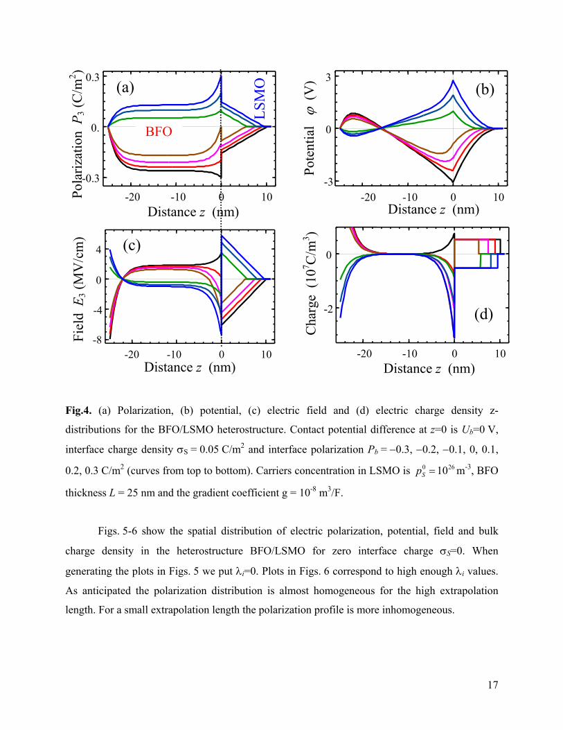
Fig. 4 shows z-dependence of the electric polarization, potential, field and bulk charge
density in the heterostructure of BFO/LSMO for different interface polarization Pb, fixed
extrapolation length and interface charge σS.
16
-20 -10 0 10
-2
0
-20 -10 0 10 -8
-4
0
4
-20 -10 0 10
-3
0
3
-20 -10 0 10
-0.3
0.
0.3 (a)
Pola
rizat
ion
P3 (
C/m
2 ) (b)
Distance z (nm)
Fiel
d E
3 (M
V/c
m)
Cha
rge
(107 C
/m3 )
(c)
Pote
ntia
l ϕ
(V
) (d)
Distance z (nm)
Distance z (nm) Distance z (nm)
LSM
O
BFO
Fig.4. (a) Polarization, (b) potential, (c) electric field and (d) electric charge density z-
distributions for the BFO/LSMO heterostructure. Contact potential difference at z=0 is Ub=0 V,
interface charge density σS = 0.05 C/m2 and interface polarization Pb = −0.3, −0.2, −0.1, 0, 0.1,
0.2, 0.3 C/m2 (curves from top to bottom). Carriers concentration in LSMO is m260 10=Sp -3, BFO
thickness L = 25 nm and the gradient coefficient g = 10-8 m3/F.
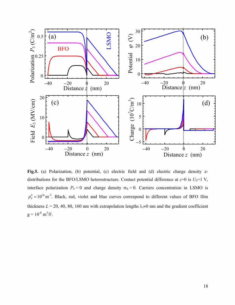
Figs. 5-6 show the spatial distribution of electric polarization, potential, field and bulk
charge density in the heterostructure BFO/LSMO for zero interface charge σS=0. When
generating the plots in Figs. 5 we put λi=0. Plots in Figs. 6 correspond to high enough λi values.
As anticipated the polarization distribution is almost homogeneous for the high extrapolation
length. For a small extrapolation length the polarization profile is more inhomogeneous.
17
- 40 - 20 0 20
- 5
0
5
10
- 40 - 20 0 20
0
10
20
- 40 - 20 0 20
0
10
20
30
- 40 - 20 0 20
0
0.25
0.5 (a) Po
lariz
atio
n P
3 (C
/m2 )
(b)
Distance z (nm)
Fiel
d E
3 (M
V/c
m)
Cha
rge
(107 C
/m3 )
(c)
Pote
ntia
l ϕ
(V
)
(d)
Distance z (nm)
Distance z (nm) Distance z (nm)
LSM
O
BFO
Fig.5. (a) Polarization, (b) potential, (c) electric field and (d) electric charge density z-
distributions for the BFO/LSMO heterostructure. Contact potential difference at z=0 is Ub=1 V,
interface polarization Pb = 0 and charge density σS = 0. Carriers concentration in LSMO is
m260 10=Sp -3. Black, red, violet and blue curves correspond to different values of BFO film
thickness L = 20, 40, 80, 160 nm with extrapolation lengths λi≈0 nm and the gradient coefficient
g = 10-8 m3/F.
18

- 40 - 20 0 20
- 0.5
0.
0.5
- 40 - 20 0 20
0
10
20
30
- 40 - 20 0 20
0
0.1
0.2
0.3
0.4
0.5
0.6 (a)
Pola
rizat
ion
P3 (
C/m
2 ) (b)
Distance z (nm)
Fiel
d E
3 (M
V/c
m)
Cha
rge
(107 C
/m3 )
(c)
Pote
ntia
l ϕ
(V
)
(d)
Distance z (nm)
Distance z (nm) Distance z (nm)
LSM
O
- 40 - 20 0 20
0
10
20
BFO
Fig.6. (a) Polarization, (b) potential, (c) electric field and (d) electric charge density z-
distributions for the BFO/LSMO heterostructure. Contact potential difference at z=0 is Ub=1 V,
interface polarization Pb = 0 and charge density σS = 0. Carriers concentration in LSMO is
m260 10=Sp -3. Black, red, violet and blue curves correspond to different thickness L = 20, 40, 80,
160 nm of BFO film with extrapolation lengths λi=30 nm and the gradient coefficient g = 10-8
m3/F.
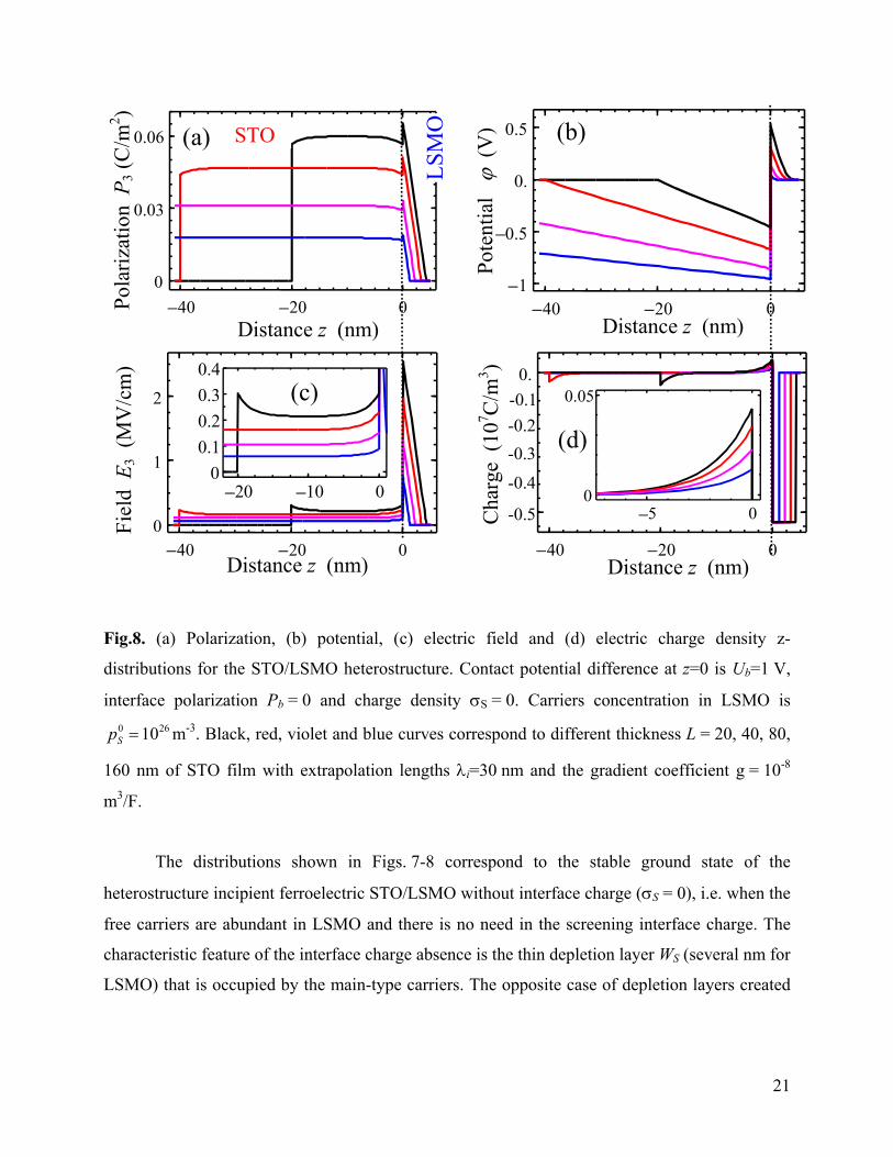
Figs. 7-8 illustrate z-distributions of the electric polarization, potential, field and bulk
charge density in the heterostructure “incipient SrTiO3 film − half-metal LaSrMnO3”
(STO/LSMO) for zero interface charge σS=0. When generating the plots in Figs. 2 we put λi=0.
Plots in Figs. 6 correspond to high enough λi values. The resulting built-in field
19

εε
− bPfL
UE bbbf
b330
~ (see Eq.(11b)) induces the electric polarization in the incipient
ferroelectric films.
- 40 - 20 0
- 0.5
0.
0.5
- 40 - 20 0
0
1
2
- 40 - 20 0
- 1
- 0.5
0.
- 40 - 20 0
0
0.01
0.05
0.02
0.03
0.04 (a)
Pola
rizat
ion
P3 (
C/m
2 )
(b)
Distance z (nm)
Fiel
d E
3 (M
V/c
m)
Cha
rge
(107 C
/m3 )
(c) Po
tent
ial
ϕ (
V)
(d)
Distance z (nm)
Distance z (nm) Distance z (nm) LS
MO
STO
Fig.7. (a) Polarization, (b) potential, (c) electric field and (d) electric charge density z-
distributions for the STO/LSMO heterostructure. Contact potential difference at z=0 is Ub=1 V,
interface polarization Pb = 0 and charge density σS = 0. Carriers concentration in LSMO is
m260 10=Sp -3. Black, red, violet and blue curves correspond to different thickness L = 20, 40, 80,
160 nm of STO film with extrapolation lengths λi≈0 nm and the gradient coefficient g = 10-8
m3/F.
20
- 40 - 20 0
-0.5
0.
-0.2
-0.4
-0.1
-0.3
- 40 - 20 0
0
1
2
- 40 - 20 0 - 1
- 0.5
0.
0.5
- 40 - 20 0
0
0.03
0.06 (a) Po
lariz
atio
n P
3 (C
/m2 )
(b)
Distance z (nm)
Fiel
d E
3 (M
V/c
m)
Cha
rge
(107 C
/m3 )
Pote
ntia
l ϕ
(V
)
Distance z (nm)
Distance z (nm) Distance z (nm)
LSM
O
- 5 0 0
0.05
(d)
- 20 - 10 0 0
0.1
0.2
0.3
0.4
(c)
STO
Fig.8. (a) Polarization, (b) potential, (c) electric field and (d) electric charge density z-
distributions for the STO/LSMO heterostructure. Contact potential difference at z=0 is Ub=1 V,
interface polarization Pb = 0 and charge density σS = 0. Carriers concentration in LSMO is
m260 10=Sp -3. Black, red, violet and blue curves correspond to different thickness L = 20, 40, 80,
160 nm of STO film with extrapolation lengths λi=30 nm and the gradient coefficient g = 10-8
m3/F.
The distributions shown in Figs. 7-8 correspond to the stable ground state of the
heterostructure incipient ferroelectric STO/LSMO without interface charge (σS = 0), i.e. when the
free carriers are abundant in LSMO and there is no need in the screening interface charge. The
characteristic feature of the interface charge absence is the thin depletion layer WS (several nm for
LSMO) that is occupied by the main-type carriers. The opposite case of depletion layers created
21
by the minor-type carriers, which can appear during the polarization reversal in the proper
ferroelectric film, will be considered in the next section.
3.3. Calculations of the metastable states for typical heterostructures (1D-case)
As it was mentioned in Sections 2-3, when the free carriers are abundant there is no need
in the screening interface charge (i.e. for thin depletion layer created by the main-type carriers
and thick layer created by the minor type carries). In the opposite case of depletion layers created
only by the minor-type carriers (i.e. without interface charge states located at z = 0) the
penetration depth WS is higher (up to tens of nanometers as shown by the bottom curves in
Figs. 9) and corresponding screening of the spontaneous polarization appeared weaker (compare
bottom curves in Fig. 9a for metastable polarization with the top curves for the stable ground
state).
Fig. 10 shows the hysteresis loops of the average polarization in the BFO film and
corresponding field penetration depth in LSMO under the absence of the interface charge σS and
two different values of the major-type carriers in LSMO. The loops asymmetry increases with the
increase of the carriers concentration [compare Figs.10a,c with Figs.10b,d]. The asymmetry of
the loops, both horizontal imprint and vertical shift, are caused by the charge effects provided by
the major- type carriers for positive biases ( ) 0>+ be UU and minor-type carriers for negative
biases ( respectively resulting in the appearance of the build-in field. ) 0<+ be UU
The weak screening causes strong electric fields, which resulting into the suppression of
polarization inside the ferroelectric film and increase of the system’s free energy, since
depolarization field energy is always positive. As a result, the strong field effect may lead to the
bend bending at z = 0 and appearance of interface charge states.
Fig. 11 shows the influence of the interface charge on the thickness dependence of the
stable and metastable (if any) states of the average polarization 3P in ferroelectric BFO film.
22
-20 0 20 40
-0.4
-0.2
0
-20 0 20 40
-4
0
4
-20 0 20 40
0
0.25
0.5
0.75
Cha
rge
(C/c
m3 )
Distance z (nm)
LSMO
Distance z (nm)
Pola
rizat
ion
P3 (
C/m
2 ) Ub=1 V (a)
(b)
Distance z (nm)
LSMO
-20 0 20 40
0
1
2
3
LSMO
Distance z (nm)
(c)(d)Fi
eld
E3 (
MV
/cm
)
Pote
ntia
l ϕ
(V
) LSMO
BFO BFO
BFO
BFO
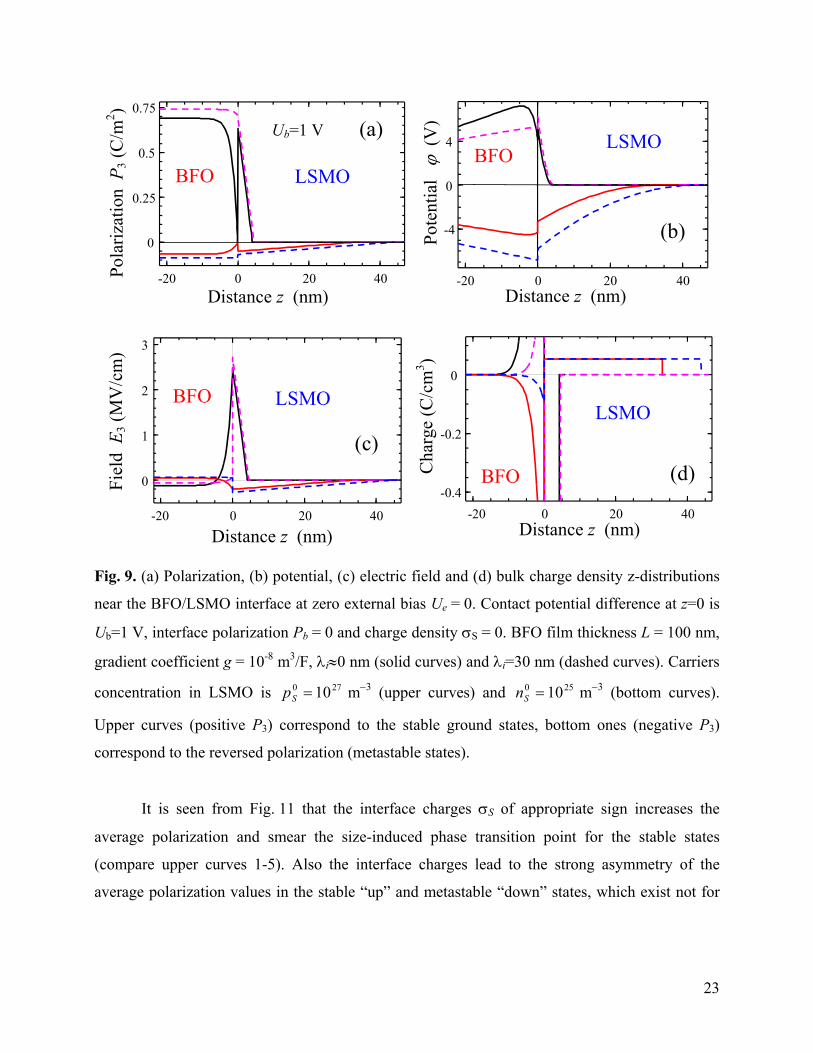
Fig. 9. (a) Polarization, (b) potential, (c) electric field and (d) bulk charge density z-distributions
near the BFO/LSMO interface at zero external bias Ue = 0. Contact potential difference at z=0 is
Ub=1 V, interface polarization Pb = 0 and charge density σS = 0. BFO film thickness L = 100 nm,
gradient coefficient g = 10-8 m3/F, λi≈0 nm (solid curves) and λi=30 nm (dashed curves). Carriers
concentration in LSMO is m270 10=Sp −3 (upper curves) and m250 10=Sn −3 (bottom curves).
Upper curves (positive P3) correspond to the stable ground states, bottom ones (negative P3)
correspond to the reversed polarization (metastable states).
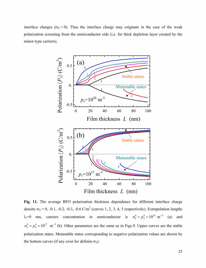
It is seen from Fig. 11 that the interface charges σS of appropriate sign increases the
average polarization and smear the size-induced phase transition point for the stable states
(compare upper curves 1-5). Also the interface charges lead to the strong asymmetry of the
average polarization values in the stable “up” and metastable “down” states, which exist not for
23

all considered values of σS (compare up and bottom curves in Figs.11). The interface charges σS
act as the contribution into the built-in field in the right-hand-side of Eqs.(10).
-20 0 20
-0.25
0
0.25
0.5
0.75
-20 0 200
50
100
-20 0 20-0.2
0
0.2
0.4
0.6 (a)
Pola
rizat
ion
P3 (
C/m
2 )
(b)
Voltage Ue+Ub (V)
Pene
tratio
n de
pth
WS (
nm)
BFO
LSMO
-20 0 20
0
50
100
Voltage Ue+Ub (V)
(c) (d)
BFO
LSMOps=1026 m-3 ps=1027 m-3
Fig. 10. Bias dependence of the average BFO polarization (a, b) and LSMO penetration depth (c,
d). BFO film thickness L = 100 nm, gradient coefficient g = 10-8 m3/F, extrapolation lengths λi≈0
nm (solid curves) and λi=30 nm (dashed curves). Interface polarization Pb = 0 and charge density
σS = 0. LSMO major-type carrier concentration is m260 10=Sp −3 (a, c) and m270 10=Sp −3(b, d);
and m250 10=Sn −3 for minor-type carriers respectively. Gap is absent (H = 0).
As expected, the interface charges σS of appropriate sign provide more effective screening
of the spontaneous polarization than the extended space-charge layer. The screening by the
interface charges σS makes polarization more homogeneous, subsequently decreases the
depolarization field, which in turn self-consistently decreases the system free energy. So the
absolutely stable profiles of reversed polarization shown in Figs.12a by the bottom curves are
more energetically preferable than the ones shown by the bottom curves in Figs.9a for zero
24
interface charges (σS = 0). Thus the interface charge may originate in the case of the weak
polarization screening from the semiconductor side (i.e. for thick depletion layer created by the
minor-type carriers).
0 20 40 60 80 100
-0.5
0.
0.5
1
34
5
1Stable states
Metastable states
0 20 40 60 80 100
-0.5
0.
0.5
13
45
145
Stable states
Metastable states
Pola
rizat
ion ⟨ P
3⟩ (C
/m2 )
Film thickness L (nm)
Film thickness L (nm)
Pola
rizat
ion ⟨ P
3⟩ (C
/m2 )
ps=1026 m-3
(a)
(b)
ps=1027 m-3
2
2
2
Fig. 11. The average BFO polarization thickness dependence for different interface charge
density σS = 0, -0.1, -0.2, -0.3, -0.6 C/m2 (curves 1, 2, 3, 4, 5 respectively). Extrapolation lengths
λi=0 nm, carriers concentration in semiconductor is m2600 10== SS pn −3 (a) and
m2700 10== SS pn −3 (b). Other parameters are the same as in Figs.9. Upper curves are the stable
polarization states. Metastable states corresponding to negative polarization values are shown by
the bottom curves (if any exist for definite σS).
25

-40 -20 0 20
-15
0
15
1
3
4
5
-40 -20 0 20
-0.5
0.
0.5
1
3
4
5
-40 -20 0 20
-5
0
5 1
3
4
5
-40 -20 0 20
-25
0
25
1
3
4
5
(a)
Pola
rizat
ion
P3 (
C/m
2 )
(b)
Distance z (nm)
Fiel
d E
3 (M
V/c
m)
Cha
rge
(107 C
/m3 )
(c)
Pote
ntia
l ϕ
(V
)
(d)
Distance z (nm)
Distance z (nm) Distance z (nm)
LSM
O
-10 0 10 20 -0.8
0.
0.8
1
34
5
1
2
2 2
2
BFO
2
Fig.12. (a) Polarization, (b) potential, (c) electric field and electric charge density (d) z-
distributions for the STO/LSMO heterostructure at zero external bias Ue = 0. Contact potential
difference at z=0 is Ub=1 V, interface polarization Pb = 0 and different interface charge density
σS = 0, +0.35, -0.35, +0.75, -0.75 C/m2 (curves 1, 2, 3, 4, 5 respectively). Carriers concentration
in LSMO is m260 10=Sp -3. BFO film thickness L = 50 nm, extrapolation lengths λi ≈ 0 nm and the
gradient coefficient g = 10-8 m3/F.
4. Effect of the incomplete screening and interface charge on the local polarization reversal
and charge transport
In the initial ground state the sluggish surface charges σf completely screen the electric
displacement outside the film. In contrast to the ground states considered in the Section 3, the
recharging of surface charges σf should appear during the local polarization reversal. The ultra-
thin dielectric gap of thickness H models the separation between the tip electrode and the
sluggish charges inside a contamination (or dead) layer.
26
The equilibrium domain structure is almost cylindrical for the case of local polarization
reversal caused by the localized potential U applied to the SPM-tip in thin ferroelectric
film [Fig. 1c]. As a sequence the spontaneous polarization distribution, the potential and the
interface charges density variations can be expressed in {x,y} - Fourier representation. In the
Fourier k
),( yxe
1,2-domain Eqs.(2, 3) immediately split into the two systems of differential equations.
The first system corresponds to the smooth components { })(),( 3 zPzϕ was solved in the previous
section. The second system for the modulating components is listed in Appendix B.
Approximate analytical solution (6) may be used in particular case of the disk-like tip
apex of radius R >> L, i.e. until 0),( ≈∆⊥ yxUe in the region of polarization reversal.
It was shown earlier [35] that the transverse polarization gradient could be neglected for
the case of the strong inequality Rg <<α2 valid for all considered ferroelectrics at room
temperature. Thus polarization ( )LzfzyxP ,~),,(3 averaged over the film thickness can be
determined from the Eqs.(10).
Using the coercive volume conception of polarization reversal formulated in Ref.[35], the
domain lateral sizes {x,y} can be estimated from the equation:
( HLEyxUHL
fcebg
g
,),(3333
33 ±=ε+ε
ε ) . (15)
The intrinsic coercive fields are given by Eq.(11b).
For a typical tip potential distribution 22
)(dr
Udre+
≈U (d is the effective tip size) the
domain radius 22 yxr += depends on applied bias U as
1)(2
33
33332 −
εε+ε
=−
±cg
bg
Ef
HLUdUr .
In general case the current density inside ferroelectric film consists of the conductivity,
diffusion and displacement, tunneling, Schottky and Frenkel-Poole emission currents [36].
During the local polarization reversal the thickness and electric charge of the space charge layer
changes, it particular the positive charge can be substituted by the negative one or vise versa
depending on the polarization direction. Such transformations should be accompanied by the
peaks of displacement currents, which shape and amplitude depend on the domain shape and
27
sizes. However, for nanoscale contact a displacement current is significantly smaller and faster
then a constant leakage current, and hence is ignored.
Derived analytical expressions also allow estimations of the tunneling current between the
tip apex and ferroelectric surface (if any exist). Assuming that the ultra-thin gap H is transparent
for the tunneling electrons, tunneling and field emission currents could flow between the tip apex
and ferroelectric film surface. In the Fowler-Nordheim transport regime [36, 37] the tunneling
current density
ϕ− ∫
−−
0* )(2
2exp~
HLt zqmdzJ
h is determined by the potential distribution ϕ(z)
given by Eq.(6) and corresponding penetration depth in semiconductor, W is
determined self-consistently from Eqs.(10).
( )HLU eS ,, ,
5. Summary
Using Landau-Ginzburg-Devonshire approach we have calculated the equilibrium
distributions of electric field, polarization and space charge in the ferroelectric-semiconductor
heterostructures containing proper or incipient ferroelectric thin films. In particular, it is shown
that space charge effects introduce strong size-effect on spontaneous polarization in 20-40 nm
epitaxial films of BiFeO3 on (LaSr)MnO3, and can induce strong polarization in incipient
ferroelectric SrTiO3.
We obtained analytical expressions for the cylindrical domain sizes appeared in
ferroelectric film under the local polarization reversal, which is caused by the electric field
induced by the nanosized tip of the SPM probe. The SPM tip can be separated from the
ferroelectric surface covered with sluggish screening charges by the ultra-thin dielectric layer that
models either geometric gap or/and contamination layer resistance.
The intrinsic field effects, which originated at the ferroelectric-semiconductor interface,
lead to the surface band bending and result in the formation of depletion/accumulation space-
charge layer near the semiconductor surface. We calculated how the build-in fields smear the
size-induced phase transition, induce polarization in the incipient ferroelectric films and lead to
the polarization hysteresis loops vertical and horizontal asymmetry in ferroelectric films.
28

Acknowledgements
Authors are grateful to Prof. E. Tsymbal for valuable critical remarks. Research is sponsored by
Ministry of Science and Education of Ukraine and National Science Foundation (Materials World
Network, DMR-0908718). SVK and AB acknowledge the DOE SISGR program.
Appendix A.
Allowing for Eq.(7), polarization distribution P3(z) should be found from the Euler-
Lagrange boundary problem (2) as:
=−=
λ−−=
=
λ+
εεσ−ρ
=−β+
εε+α
.0,0
,1
323
313
330
0
32
23
33330
LzdzdP
PPzdz
dPP
WP
dzd
gPP
b
bSSS
b
(A.1)
Let us look for the solution of the problem (A.1) in the form ( ) ( )zpPzP += 33 , where the
average polarization ∫−
≡0
33~)~(
1
L
zdzPL
P is introduced. The variation p average value is zero:
0≡p . So, the problem (A.1) acquires the form:
( )
−=−=
λ−−−=
=
λ+
β+α−εε
−σ−ρ=−β+β+
εε+β+α
.,0
,31
3
3231
333
330
30
2
232
3330
23
PLzdz
dppPP
zdzdp
p
PPPW
dzpd
gppPpP
b
bSSS
b
(A.2)
Since always 01
330
>>εε
+αb
(as well as 01
3330
23 >>
εε+β+α
bP ) for both proper and incipient
ferroelectrics, Eq.(A.2) can be linearized with respect to the deviation p and then solved by
standard methods.
After elementary transformations, polarization distribution acquires the form:
( ) ( )( ) ( )
−≥−θ⋅−−
−≥−θ⋅−
ε−ε
=carrierstypepofdepletion,0,
carrierstypenofdepletion,0,1)(
0
0
3zzWWzn
zzWWzpqzP
SnSnS
SpSpS
S
S (A.3)
29
( ) ( ) 0),,(,13
2)( 2
3330
033330
3 ≤<−⋅−+β+αεε
σ−ρ+βεε= zLLzbPLzf
P
WPzP bb
SSSb
. (A.4)
The space distribution is governed by the functions f and b:
( ) ( )( ) ( ) ( )( ) ( )( )( ) ( ) ( ) ( )ξλ+λξ+ξλλ+ξ
ξ−ξ+ξ+ξλ+ξ+λξ−=
LLzzLzzLLzf
coshsinhsinhsinhcoshcosh1,
21212
12 , (A.5a)
( ) ( )( ) ( )( )( ) ( ) ( ) ( )ξλ+λξ+ξλλ+ξ
ξ+ξ+ξ+ξλ=
LLzLzLLzb
coshsinhsinhcosh,
21212
22 . (A.5b)
Characteristic length ( ) gP
g bb
b
33023330
330
13εε≈
+β+αεε
εε=ξ .
Then the average polarization 3P and depths WSn,p should be determined self-
consistently from the spatial averaging of Eq.(8b),
( ) bPfP
WPP bb
SSSb
⋅−+β+αεε
σ−ρ+βεε=
13
22
3330
033330
3 , and boundary conditions (4b,c).
For particular case H = 0 this gives the system of coupled algebraic equations:
( )
εε+β+α⋅−
εεσ−ρ
=
εε+−β+α
=
εε
+σ−
εερ
+εε
ρ−
.1
31
23
,2
330
23
330
0
330
233
330
3
330
0
0
20
bbbSSS
b
bbS
bSS
S
SS
PbPfW
fPP
UPW
LW
(A.6)
Where ( )( ) ( ) ( )( )
( ) ( ) ( ) ( )( )( )
( )( )212
21
212
212
21
212 2
1sinhcosh
sinh1cosh21
λλ+ξ+λ+λξ
λ+λ+ξξ−≈
ξλλ+ξ+ξλ+λξ
ξλ+λ+−ξξξ−=
LLLLLL
f and
( ) ( )( )( ) ( ) ( ) ( )( )
( )( )( ) ( )1
2
21212
22
21212
32
2
coshsinhcosh1sinh
λ+ξξ
=λ+λξ+λλ+ξ
λ+ξξ≈
ξλ+λξ+ξλλ+ξξ−ξ−ξλξ
=LLLLL
LLb .
The system (A.6) reduces to the relations
( )
εε−
εεσ−ρ
=−β+
εε+α
εε−ερε
+ρ+σ−=
.231
,2
330330
03
33330
3302
0330
3
bb
bSSS
b
bbS
S
Sb
SSS
bPf
WfPP
LU
WL
WP
(A.7)
30

Since L
UW
LWP bb
SS
Sb
SSS 3302
0330
3 2εε−
ερε
+ρ+σ−= and 01
03303 >ρ
εε+σ+
S
bbS L
UP
, the second
of Eqs.(14) reduces to six order algebraic equation for the built-in field determination.
The polarization contribution into the relative atomic displacement u3 can be estimated as
)()( 33 zPQV
zuBS
S≈ at z > 0 and )()( 33 zPQV
zuBIF
FE≈
29104 −⋅
at –L < z < 0. Here Vj is the volume of the
corresponding unit cell, QB is the Born effective charge of the lightest atom “B”. For perovskites
considered hereinafter V m, .6≈SFE3
Appendix B.
The potential applied to the SPM-tip is highly-localized, i.e.
. As a sequence the spontaneous polarization
distribution can be approximated as ,
the potential ϕ and the interface charges
density variation can be expressed in Fourier
representation (see).
(∫∫∞
∞−
∞
∞−
−−= yikxikudkdkyxU 2121 exp)(),( k
PS (
∫∫∞
∞−
∞
∞−
+ϕ= dkdkzzyxf 1)(),,(
∫∫∞
∞−
∞
∞−
σ=δσ dkdkyxS 21~),(
)
( )∫∫∞
∞−
∞
∞−
−−+= yikxikzpdkdkzPzyx S 21213 exp),()(),, k
( )−−ϕ yikxikz 212 exp),(~ k
( )−− yikxikS 21exp)(k
In the Fourier k1,2-domain Eqs.(3) immediately split into the two systems of differential
equations. The first system corresponds to the smooth components { })(),( 3 zPzϕ was solved in the
previous section. The second system for the modulating components is:
.0,0~~
,0,),(1~~
,,0~~
22
20
2112
2
33
22
2
>=ϕ−ϕ
<<−ε
=ϕε−ϕ
ε
−<<−−=ϕ−ϕ
zkdzd
zLzd
zdpkdzd
LzLHkdzd
Sb k (B.1)
31
Where . Rewritten for the modulating components, the boundary conditions (4)
acquire the form:
22
21
2 kkk +=
( )( ) ( )
( ) ( )
( ) .0,~
,00,~0,~),(~)0,()0,(~)0,(~
),(~),()0,(~)0,(~
,00,~0,~),(,~
330
33330
=∞→ϕ
≈−ϕ−+ϕσ=−
−ϕε−
+ϕεε
σ=−−
−−ϕε−
+−ϕεε
≈−−ϕ−+−ϕ=−−ϕ
zk
kkkpdzkd
dzkd
Lkpdz
Lkddz
LkdLkLk
kuHLk
SSSb
fSgb
k
k (B.2)
Where the gap dielectric permittivity ε is introduced. g33
LGD-equation (2) for determination of the modulation pS(k,z) acquires the form:
[ ]
[ ]
0,00
.)'()'(')(3)"()"'(")'('),(
,),(),(~),()(3
21
3
2
22
32
=−=
λ−=
=
λ+
−+−−=
β−ϕ−=
−β++α
∫∫∫∞
∞−
∞
∞−
∞
∞−
Lzdzdp
pzdz
dpp
ppdzPppdpdzpQ
zpQzdzd
zpdzd
gzPkg
SS
SS
SSSSSS
SS
kkkkkkkkkkkk
kkk
(B.3)
The value should be determined self-consistently. In the final state the distribution of
the surface charge
),( LpS −k
)(~ kfσ localized at Lz −= and the interface charge )(~ kSσ localized at 0=z
should provide the most effective screening of the spontaneous polarization outside the film and
minimal depolarization field energy.
The expression for the bias-dependent barrier height related with applied bias difference
and polarization changes is given by expression
( )
−−−−ϕ≈Φδ ∫∫
∞
∞−
∞
∞−
),(exp),(~),( 2121 yxUyikxikLdkdkqyxB k . (B.4)
References
1 A. Ohtomo, D. A. Muller, J. L. Grazul & H. Y. Hwang. Artificial charge-modulation in atomic-
scale perovskite titanate superlattices. Nature 419, 378, (2002).
32
2 A. Ohtomo and H.Y. Hwang, A high-mobility electron gas at the LaAlO3/SrTiO3
heterointerface. Nature 427, 423 (2004).
3 H. Y. Hwang, Atomic control of the electronic structure at complex oxide heterointerfaces.
Mater. Res. Soc. Bull. 31, 28–35 (2006).
4 S. Okamoto, A. J. Millis, Electronic reconstruction at an interface between a Mott insulator and
a band insulator. Nature 428, 630–633 (2004).
5 R.G. Moore, Jiandi Zhang, V. B. Nascimento, R. Jin, Jiandong Guo, G.T. Wang, Z. Fang, D.
Mandrus, E. W. Plummer. A Surface-Tailored, Purely Electronic, Mott Metal-to-Insulator
Transition. Science 318, 615 (2007).
6 V. Garcia, S. Fusil, K. Bouzehouane, S. Enouz-Vedrenne, N. D. Mathur, A. Barthélémy, and
M. Bibes. Giant tunnel electroresistance for non-destructive readout of ferroelectric states. Nature
460, 81-84 (2009).
7 P. Maksymovych, S. Jesse, Pu Yu, R. Ramesh, A.P. Baddorf, S.V. Kalinin. Polarization
Control of Electron Tunneling into Ferroelectric Surfaces. Science 324, 1421 - 1425 (2009).
8 A. Gruverman, D. Wu, H. Lu, Y. Wang, H. W. Jang, C. M. Folkman, M. Ye. Zhuravlev, D.
Felker, M. Rzchowski, C.-B. Eom and E. Y. Tsymbal, Tunneling Electroresistance Effect in
Ferroelectric Tunnel Junctions at the Nanoscale. Nano Lett., 9 (10), pp 3539–3543 (2009).
9 T. Choi, S. Lee, Y. J. Choi, V. Kiryukhin, S.-W. Cheong, Switchable Ferroelectric Diode and
Photovoltaic Effect in BiFeO3. Science 324, 63 - 66 (2009).
10 J.F. Scott, Ferroelectric Memories. Springer Series in Advanced Microelectronics: Vol. 3,
(Springer Verlag, 2000) 248 p. ISBN: 978-3-540-66387-4.
11 P. W. M. Blom, R. M. Wolf, J. F. M. Cillessen, and M. P. C. M. Krijn, Ferroelectric Schottky
Diode. Phys. Rev. Lett. 73, 2107 (1994).
12 P. Zubko, D.J. Jung, and J.F. Scott, Space Charge Effects in Ferroelectric Thin Films. J. Appl.
Phys. 100, 114112 (2006).
13 P. Zubko, D.J. Jung, and J.F. Scott, Electrical Characterization of PbZr0.4Ti0.6O3 Capacitors.
J. Appl. Phys. 100, 114113 (2006).
14 Y. Watanabe. Theoretical stability of the polarization in a thin semiconducting ferroelectric.
Physical Review B 57, 789 (1998)
33
11 3E
15 J. Bardeen, Surface States and Rectification at Metal Semi-Conductor Contact. Phys. Rev. 71,
717 (1947)
16 V.M. Fridkin, Ferroelectrics semiconductors, Consultant Bureau, New-York and London
(1980). p.119
17 M.A. Itskovsky, Fiz. Tv. Tela, 16, 2065 (1974).
18 The dependence of ε on is absent for uniaxial ferroelectrics. It may be essential for
perovskites with high coupling constant.
19 Chun-Gang Duan, Renat F. Sabirianov, Wai-Ning Mei, Sitaram S. Jaswal, and Evgeny Y.
Tsymbal. Interface Effect on Ferroelectricity at the Nanoscale. Nano Letters 6, 483 (2006)
20 Chun-Gang Duan, S. S. Jaswal, and E.Y. Tsymbal. Predicted Magnetoelectric Effect in
Fe/BaTiO3 Multilayers: Ferroelectric Control of Magnetism. Phys. Rev. Lett. 97, 047201 (2006)
21 M.D. Glinchuk, A.N. Morozovska, J. Phys.: Condens. Matter. 16, 3517 (2004).
22 M.D. Glinchuk, A.N. Morozovska, and E.A. Eliseev, J. Appl. Phys. 99, 114102 (2006)
23 S. M. Sze, Physics of Semiconductor Devices, 2nd ed. (Wiley-Interscience, New York, 1981),
Chap. 7, p. 382.
24 S. Ducharme, V. M. Fridkin, A.V. Bune, S. P. Palto, L. M. Blinov, N. N. Petukhova, S. G.
Yudin, Phys. Rev. Lett. 84, 175 (2000).
25 A. K. Tagantsev, G. Gerra, and N. Setter, Short-range and long-range contributions to the size
effect in metal-ferroelectric-metal heterostructures. Phys. Rev. B 77, 174111 (2008).
26 E.A. Eliseev, M.D. Glinchuk, А.N. Morozovska. Appearance of ferroelectricity in thin films
of incipient ferroelectric. Phys. stat. sol. (b) 244, № 10, 3660–3672 (2007).
27 J. L. Cohn, M. Peterca, and J. J. Neumeier, Phys. Rev. B 70, 214433 (2004).
28 A. Tiwari, C. Jin, D. Kumar, and J. Narayan. Appl. Phys. Lett. 83, 1773 (2003).
29 A. Ruotolo, C.Y. Lam, W.F. Cheng, K.H. Wong, and C.W. Leung. Phys. Rev. B 76, 075122
(2007).
30 T. Muramatsu Yuji Muraoka, Zenji Hiroi. Solid State Communications 132, 351–354 (2004).
31 Kui-juan Jin, Hui-bin Lu, Qing-li Zhou, Kun Zhao, Bo-lin Cheng, Zheng-hao Chen, Yue-liang
Zhou, and Guo-Zhen Yang. Phys. Rev B 71, 184428 (2005).
32 G.A. Smolenskii, V.A. Bokov, V.A. Isupov, N.N Krainik, R.E. Pasynkov, A.I. Sokolov,
Ferroelectrics and Related Materials (Gordon and Breach, New York, 1984). P. 421
34
33 C.-L. Jia, Valanoor Nagarajan, J.-Q. He, L. Houben, T. Zhao, R. Ramesh, K. Urban, R.
Waser, Unit-cell scalemapping of ferroelectricity and tetragonality in epitaxial ultrathin
ferroelectric films. Nature Mat 6, 64-69 (2007).
34 M.D. Glinchuk, E.A. Eliseev, A. Deineka, L. Jastrabik, G. Suchaneck, T. Sandner, G. Gerlach,
M. Hrabovsky. Optical refraction index and polarization profile of ferroelectric thin films.
Integrated ferroelectrics 38, 101-110, (2001).
35 A.N. Morozovska, E.A. Eliseev, Yulan Li, S.V. Svechnikov, V.Ya. Shur, P. Maksymovych,
V. Gopalan, Long-Qing Chen, S.V. Kalinin. Thermodynamics of nanodomain formation and
breakdown in scanning probe microscopy: Landau-Ginzburg-Devonshire approach. Phys. Rev. B.
80, № 21. 214107-1-12 (2009).
36 M. Grossmann, O. Lohse, D. Bolten, and U. Boettger, R. Waser. The interface screening
model as origin of imprint in PbZrxTi1-xO3 thin films. II. Numerical simulation and verification J.
Appl. Phys. 92, 2688 (2002).
37 I.C. Infante, F. Sanchez, V. Laukhin, A. Perez del Pino, and J. Fontcuberta, K. Bouzehouane,
S. Fusil, and A. Barthelemy. Functional characterization of SrTiO3 tunnel barriers by conducting
atomic force microscopy. Appl. Phys. Lett. 89, 172506 (2006).
35