FINAL REPORT - ntrs.nasa.gov · FINAL REPORT f. TITLE OF GRANT ... A. B. C. D. E. F. G. H. I. J....
64
,,,,-j_7,/_/2J S_ L ,C- FINAL REPORT f. TITLE OF GRANT Further Improvements in Program to Calculate Electronic Properties of Narrow Band Gap Materials ur_ ,-4 ,,o o r_ el I ao Z _ 0 NAME TYPE OF REPORT Brief Summary of Entire Project NAME OF PRINC!.PAL INVESTIGATOR James D. Patterson September 15, 1992 PERIOD COVERED BY THE REPORT June 15, 1991 - June 15, 1992 (plus extension of up to six months) AND ADDRESS OF GRANTEE INSTITUTION Florida Institute of Technology 150 W. University Boulevard Melbourne, FL 32901 O w_ _C _w _Z< Z_ I>_ _0_ rq 0 .,._ qn O- I-,. 0 ,-.4 m o o 2L,-- I) U.. f GRANT NUMBER NAG8-781 Supplement 2 George C. Marshall Space Flight Center Marshall Space Flight Center, AL 35812 (Technical Officer Sa0dor L. Lehoczky, ES75) https://ntrs.nasa.gov/search.jsp?R=19920024371 2018-05-31T11:50:23+00:00Z
-
Upload
phungthuan -
Category
Documents
-
view
215 -
download
0
Transcript of FINAL REPORT - ntrs.nasa.gov · FINAL REPORT f. TITLE OF GRANT ... A. B. C. D. E. F. G. H. I. J....
,,,,-j_7,/_/2J S_ L ,C-
FINAL REPORT
f.TITLE OF GRANT
Further Improvements in Program to Calculate ElectronicProperties of Narrow Band Gap Materials
ur_,-4,,o or_ el
I ao
Z _ 0
NAME
TYPE OF REPORT
Brief Summary of Entire Project
NAME OF PRINC!.PAL INVESTIGATORJames D. Patterson
September 15, 1992
PERIOD COVERED BY THE REPORT
June 15, 1991 - June 15, 1992
(plus extension of up to six months)
AND ADDRESS OF GRANTEE INSTITUTION
Florida Institute of Technology150 W. University Boulevard
Melbourne, FL 32901
O
w__C
_w
_Z<
Z_
I>__0_
rq
0
.,._
qn
O- I-,.
0
,-.4
m
o o2L,--I) U..
f
GRANT NUMBER
NAG8-781 Supplement 2
George C. Marshall Space Flight CenterMarshall Space Flight Center, AL 35812
(Technical Officer Sa0dor L. Lehoczky, ES75)
https://ntrs.nasa.gov/search.jsp?R=19920024371 2018-05-31T11:50:23+00:00Z
Personnel
James D. Patterson, Principal InvestigatorProfessor and Head, Physics and Space Sciences Department
Florida Institute of Technology
Wafaa Abdelhakiem Gobba, Post Doctoral Research Associate
Physics and Space Sciences DepartmentFlorida Institute of Technology
ABSTRACT
We list and discuss the tasks we have accomplished and considered. In some areas
more has been accomplished than others. An extra task was a calculation comparingelectron mobilities in Mercury Manganese Telluride with Mercury Cadmium Telluride
given in 1H. We then list the reports and papers produced and follow that with eitherabstracts or the papers themselves. In one key paper we obtain good results betweenexperiment and theory in Mercury Zinc Telluride and also find it typically has mobilities
competitive with Mercury Cadmium Telluride. In the appendix we haye a relatively
complete set of references.
Outline
L
II.
II1.
IV.
List of Tasks Accomplished/Considered ............................................. 1
A.
B.C.D.E.
F.G.H.I.
J.
Characterization of Donors and Acceptors ............................ 1Electron-Longitudinal Optic Mode Scattering ....................... 4Alloy Disorder Scattering .......................................................... 21Other Scattering Mechanisms .................................................. 23Further Work on MZT ................................................................. 24
Experimental Data ...................................................................... 25Superlattices ................................................................................ 27MMT and Parameter Table ........................................................ 33References ................................................................................... 53
Availability of Program ............................................................... 54
List of Reports and Papers .................................................................... 55
Abstracts of Papers, Reports and Other Documents ........................ 56
Suggestions for Future Work ................................................................ 79
Appendix ................................................................................................... 80List of References .................................................................................... 81

•
I. LIST OF TASKS ACCOMPLISHED/CONSIDERED
A. Characterization of Donors and Acceptors
The study of donors and acceptors in narrow gap semiconductors is by no means
simple. Misplaced Hg in MCT seems to be a major cause of intrinsic doping. Hgvacancies can produce a p type material and extra Hg interstitials an n type. Indiumdoping has caused p type MCT to become n type as expected. A little more generally,
group I and II elements should be acceptorsand donors on Hg, Cd (group II) metalsites while V and VII elements should be acceptors and donors on Te (group VI) sites.The situation is very complicated, however, and experiment is needed to verify thesesuppositions. Furthermore, the situation is complicated by the fact that we can haveboth deep and shallow states. Vacancies, interstitials and even substitutional
impurities can cause deep levels. In any case deep levels produced by a short rangepotential, are often not well characterized, and usually produce a level near the middleof the gap. If we neglect deep levels, we are still left with shallow levels. Shallowstates can, at least for small x, merge with the conduction band. We can understandthis merger as related to the Mott transition. When the density of defects increases,discrete levels may become broadened and produce energy states that may join with,for example, the conduction band in the case of donors. In fact, it has been predicted
that Hgl.xCdxTe with a (shallow) donor concentration of at least 1014 cm °3 would not
have bound states and this seems to be well confirmed experimentally. In generalthere appears to be no freezeout of carriers on shallow impurities for bandgaps in, asgrown, MCT which has x < .2. There are in fact other reasons for the merging with theconduction band. Donor levels can be screened by electrons in the conduction bandand this screening can decrease the binding energy. We have examined this in apaper referenced below. In addition, when the binding energy gets small enough thedonor wave functions may hybridize with the band functions and again we getmerging.
Note about shallow donors.
The simplest theory of shallow impurities characterizes them as hydrogenic. For non-degenerate bands with parabolic dispersion relations, the "envelope" function of theimpurities satisfies;
2[- _2 _2_ e ]F = EF
.#
Kr2rn
where m is the effective mass and K is the (relative) dielectric constant.

2,
For a ls ground state, the binding energy is
_t
13,600 m
K 2 momev
with wave function
l r/aBFls = e
where
m oaB= 0.53 x K x_A
m
Our situation has many complications beyond this (Bastard p. 119-120). We don'thave parabolic bands and the donors are often not well characterized. Anothercomplication arises from the fact that in the _cornpound semiconductors that weconsider, the lattice is charged so electrons interact with it even at absolute zero. Thus
the stationary states are polarons. The effect of the lattice can only be neglected fortightly bound electrons - not the usual case for shallow donors. For weak binding onemust view the situation as a polaron bound in a hydrogenic orbit
SUMMARY - SHALLOW LEVEL DEFECTS
These have a long range potential and their wave function spreads over many
neighboring atoms.
Have a hydrogen like spectrum as modified by dielectric constant and effective mass.
Usually have ionization energies much less than the gap energy.
Connected to the adjacent band (that is Eigenfunction mix with nearest band states).
Due to screening and hybridization may merge with nearest band.
They control conductivity.
Note about deeper levels.
The nature of donors in Gal_xAIxAS can be quite different depending on the x value
(Weisbuch and Vinter, 47-50). For Si donors the energy levels can change from 6meV to 160 meV as one changes from direct to indirect materials. The transition takes
place at about x = 0.24. _

,
Erbarut has treated the electronic structure of ideal vacancies in MCT. His work isbased on an extension of the Slater-Koster model and does not include lattice
relaxation. The energy levels obtained areoften in the range of deep bound levels.
At any rate, deep levels are often treated along Slater-Koster lines. Effective masstechniques are often not appropriate for deep levels. Hjalmarson has defined a deep
impurity to be one "whose short-range central-cell potential alone is sufficiently strongto bind a state".
SUMMARY - DEEP LEVEL DEFECTS
Short range potential, wave function relatively well localized.
Not a hydrogen like spectrum - use tight binding approximation.
Often have ionization energy comparable to half the gap energy.
Connected to the conduction band and valence band.
Often hard to even identify a model for center.
They control lifetime of carriers.
General note.
Capper has given a review of impurity behavior in bulk MCT. He points out that"extensive doping using elements which provide stability of electrical properties will
become increasingly important in future infrared devices based on MCT." A common
way to study defects is by photolumin@scenCe spectra as discovered by Werner et al.Native defects are highly sensitive to deviations in stochiometry and to stress. Pointdefects come in a variety of forms; lattice defects (vacancy, self interstitial and antisite)
and foreign atom (substitutional and interstitial).
Donors, acceptors and other defects can be important in lowering the mobility at lowtemperature, but other scattering mechanisms are much more important at highertemperatures. Defects determine to a large extent the quality of these materials forinfrared detectors.
\ 3ao
REFERENCES
o J.D. Patterson and Wafaa A. Gobba, "Enhanced Screening in Doped
Semiconductors," Bull. Am. Phys. Soc. 37 (1), 196 (1992).
+ E. Erbarut, "Electronic Structure of the Ideal Vacancies in
(Hg, Cd) Te," phys. stat. sol. (b) 164, 235-241 (1991).
+
°
.
P. Capper, "A Review of Impurity Behavior in Bulk and Epitaxial Hg l_xCdxTe, " J.
Vac. Sci. Technol. B9(3), 1667-1681 (1991).
L. Werner, J.W. Tomm and K.H. Herrmann, "Identification of the Nature of the
Optical Transitions in Hgo.42Cdo.58Te," Infrared Phys. 31(1), 49-58 (1991).
M.A. Berding, M. van Schilfgaarde, A.T. Paxton, and A. Sher, "Defects in ZnTe,CdTe, and HgTe: Total Energy Calculations," J. Vac. Sci. Technol. A8(2) 1103-1107 (1990).
. C.L. Littler, D.G. Seiler, and M.R. Loloee, "Magneto-optical Investigation of
Impurity and Defect Levels in HgCdTe Alloys," J. Vac. Sci. Technol. A8(2),1133-1138 (1990).
o
,
J.B. Choi and H.D. Drew, "Donor Spectroscopy in Hgl.xCdxTe at High Magnetic
Fields," Phys. Rev. B. 41, 8229-8239 (1990).
I.M. Tsidilkovski, G.I. Harus and N.G. Shelashina, "Impurity States and Electron
Transport in Gapless Semiconductors," Advances in Physics 34, 43-174 (1985).
, J.R. Lowney, A.H. Kahn, J.L. Blue_ and C.L. Wilson, "Disappearance of ImpurityLevels in Silicon and Germanium Due to Screening," J. of Applied Phys. 52,
4075-4080 (1981).
10. H.P. Hjalmarson, P. Yogi, D.JI Wolford and J.D. Dow, Theory of Substitutional
Deep Traps in Covalent Semiconductors," Phys. Rev. Letters 44,810-813(1980).
11.
12.
13.
A.J. Syilaios and M.J. Williams, "Conductivity type conversion in (Hg, Cd) Te," J.Vac. Sci. Technol. 21 (1), 201-204 (1982).
C.A. Swarts, M.S. Daw, and T.C. McGill, "Bulk vacancies in CdxHgl-xTe," J.
Vac. Sci. Technol. 21 (1), 198-200 (1982).
S.T. Pantelides, "The electronic Structure of impurities and other point defects insemiconductors," Rev. Modern Phys. 50,797-858 (1978).
41
B. Electron-Longitudinal Optic Mode Scattering
We have studied the Random Element Isodisplacement Model of two-mode behavior.We have also reviewed models for establishing criteria for two mode versus one modebehavior. We have studied effective charges and their meaning for scatteringelectrons. We have also reviewed the literature. All of these things are discussed inmore detail below.
1. Szigeti, Transverse and Callen Effective Charge
Ionic polarizability is caused by the displacements of the ions as a whole whileelectronic polarizability is caused by the displacement of the electron cloud
relative to the nuclei. The displacement of the ions changes the interatomicdistance which in turn affects the distn'bution of the electron cloud. This effect is
a short range interaction, since it only depends on the displacement of the nearneighbors. There is another type of interaction between atomic and electronicpolarizations through the internal field. This effect is a long range effect sincethe distant dipoles as well as the near dipoles contribute.
Szigeti defined a correction factor s for deviation from heteropolar behavior as aresult of mutual distortions of neighboring ions due to their overlapping. Szigeticharge represents the short range interaction of the electronic and atomicdisplacements. One might expect to find s very different from one if the ionspenetrate considerably into each other or if the bond has partial homopolarcharacter and its polarity changes rapidly with the distance between the atoms.Szigeti has shown how the factor s can be obtained in terms of values that canall be experimentally measured.
The transverse charge is defined to give the local polarization (electronic andatomic) caused by relative displacements. The polarization includes that due to
ionic motion and that induced in the electronic charges in the absence ofelectric fields. The resulting field which scatters electrons is accounted for by
separately dividing by co (giving rise to the definition of the Callen charge).

1
The Szigeti effective charge e s = se is used in computing the force on a ion. Distortion
of the charge affects the value of e s and causes s _ 1. The distortion is due to overlap.
By Born and Huang
!o _ l { sze (u. - u_ ) + (o_, + o(_ ) 4----V--_P
v a 3
Assuming E = 0, :x + are the polarizability of the ions and u+
displacement of the ions, z is the charge of the ions and v<x
molecule. Solving for p gives us
- u. is the relative
is the volume per
1 sze (u+ - u_ )p-
v_ i- 4---E-_ (_÷+__)
3v_
Then using the Clausius-Mosotti equation
4_: (:+ + :_ ) Coo- I- Vc _
3 Coo+2
This means that the polarization can be written
p _ l sze (:oo + 2) (u,v a 3
-u_)
The quantity
coo + 2 coo + 2e T - Se - e s
3 3
is called the transverse charge. Thus
i° =_z e T (u.V a
-U_)
This P produces a field which scatters electrons. But in calculating this field we must
divide by coo since it is long range and the field is affected by other electrons. So

o
another relevant charge, called the Callen charge is
e c = eT/Coo
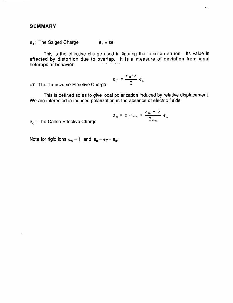
SUMMARY
es: The Szigeti Charge e s = se
This is the effective charge used in figuring the force on an ion. Its value isaffected by distortion due to overlap. It is a measure of deviation from idealheteropolar behavior.
eT: The Transverse Effective Charge
coo+2eT - e s
3
This is defined so as to give local polarization induced by relative displacement.We are interested in induced polarization in the absence of electric fields.
ec: The Callen Effective Charge
ec eT/coo coo + 2= - eS3_oo
Note for rigid ions _= = 1 and e c = e T = e s.
Q
2. One and Two Mode Behavior
In binary alloy systems, lattice vibration spectra can show two differentbehaviors. The first is "one mode behavior' in which the phonon frequencychanges continuously from the value that corresponds to one end member tothat of the other end member with an approximately constant strength. Thesecond is "two mode behavior' in which two frequencies occur with a strength
approximately equal to the fractional composition of each component.
Experimentally, this behavior can be seen through infrared and Ramanspectroscopy. A Kramers-Kronig dispersion analysis can be applied to
reflection spectra to get the real part of the dielectric constant Re c(_J), the
imaginary part of the dielectric constant Im c(uo), and the imaginary part of the
reciprocal of the dielectric constant -Im (1/c(co)). From these functions thefrequencies of the transverse optical phonons (TO) and those of longitudinaloptical (LO) phonons are determined. The frequencies of the TO phonons are
determined from the positions of the maxima of the Im c(_) curve and the
frequencies of the LO phonons from the positions of maxima of -Im (]/c(_)) or
from the points where the Re c(_o) curve crosses the co - axis. In the case ofthe two mode behavior, the Kramer-Kronig analysis yields for each x - value twofrequencies of the transverse optical phonons (TO 1 and TO2) and two
frequencies of the longitudinal optical phonons (LO 1 and LO2).
Now returning to the ideas of one and two mode behavior. Consider the
pseudobinary compound ABI.xC x composed of atoms A, B, and C. Two mode
behavior in ABI_xC x may also be seen experimentally in reflectivity spectra.
Supposedly, this means the interactions of a cation with one anion and a cationwith another anion are independent, thus the AB and AC vibrations areindependent. Actually one may see one or two mode behavior depending onthe situation.
In one mode behavior the frequencies of long wave length phonons varycontinuously from x = 0 (AB) to x = 1 (AC).
In two mode behavior one has two sets of phonon frequencies for each x _ 0 or1. The set that starts from x = 0 starts from AB type behavior and the set from x --1 starts from BC type behavior. The mole fractions of AB and AC determine by
proportionality the strength of the frequencies.

" 9,
A sketch of the two kinds of behavior looks like:
CO
GFvP MopZ
o l _'X
oCa)
-- ....
/0
LocRC MobE
"/-oJ O //Jl :' ,.?
"I£E _l r} ,l ".V.,o _
The following convention is used in naming modes. An impurity mode lying
above the optic band of the host lattice is a local mode. Note this occurs atx = 1. A gap mode lies below the band of the host lattice. Note this occurs atx = 0. There are also more complicated situations. Obviously one can reverse
directions by letting x ---, x' = I-x , 1 - x -, x'.
The actual criteria for one - and two- mode behavior can be somewhat
complicated.
Let
= 1 - 1'/1
where M' > M c < 0
and for M' < M 0 < e < 1.
10.
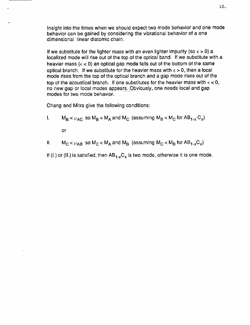
Insight into the times when we should expect two mode behavior and one modebehavior can be gained by considering the vibrational behavior of a onedimensional linear diatomic chain.
If we substitute for the lighter mass with an even lighter impurity (so c > 0) alocalized mode will rise out of the top of the optical band. If we substitute with a
heavier mass (c < 0) an optical gap mode falls out of the bottom of the same
optical branch. If we substitute for the heavier mass with c > 0, then a localmode rises from the top of the optical branch and a gap mode rises out of the
top of the acoustical branch. If one substitutes for the heavier mass with _ < 0,no new gap or local modes appears. Obviously, one needs local and gapmodes for two mode behavior.
Chang and Mitra give the following conditions:
I. MB<PA C SOMB<MAandM C (assuming MB<McforABI_xCx)
or
I1. MC < _AB so M C < M A and M B (assuming MC < M B for ABI_xCx)
If (I.) or (11.)is satisfied, then ABI_xC x is two mode, otherwise it is one mode.
11.
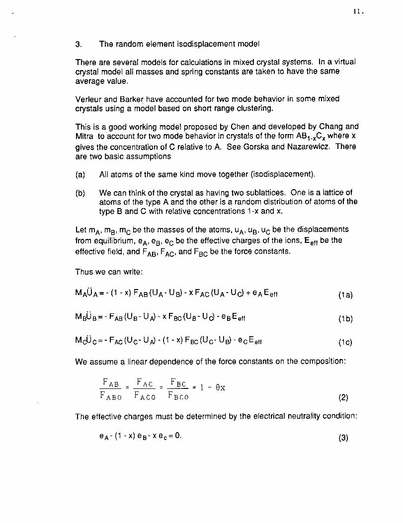
3. The random element isodisplacement model
There are several models for calculations in mixed crystal systems. In a virtual
crystal model all masses and spring constants are taken to have the sameaverage value.
Verleur and Barker have accounted for two mode behavior in some mixed
crystals using a model based on short range clustering.
This is a good working model proposed by Chen and developed by Chang andMitra to account for two mode behavior in crystals of the form ABI.xC x where x
gives the concentration of C relative to A, See Gorska and Nazarewicz. Thereare two basic assumptions
(a)
(b)
All atoms of the same kind move together (isodisplacement).
We can think of the crystal as having two sublattices. One is a lattice ofatoms of the type A and the other is a random distribution of atoms of thetype B and C with relative concentrations 1-x and x.
Let mA, m B, m C be the masses of the atoms, u A, u B, uC be the displacements
from equilibrium, e A, e B, e C be the effective charges of the ions, Eef f be the
effective field, and FAB, FAC, and FBC be the force constants.
Thus we can write:
MAOA=- (1 - x) FAB(U A- UB)- x FAc(U A- UC) + eAEeff
MBOB=- FAB(U B- UA)- X FBc(U B- Uo.)- eBEeff
(1 a)
(lb)
FABO FAC0 FBCO (2)
The effective charges must be determined by the electrical neutrality condition:
e A - (1 - x) e B- x ec = 0. (3)
FAB - FAC - FBC - I - 0x
MC0C=- FAc(Uc- UA)- (1 - x) FBc(U c- UB)- ecEef f (lc)
We assume a linear dependence of the force constants on the composition:

12.
We start out by looking at long-wavelength transverse optical phonons forwhich E ,_ 0. For this case
P = N [ eAU A - (I - X) eBU B - x ecU ¢ ] + N_ Eel f (4a)
where
Eef f = E + 4---E_P- 4n p3 3 (4b)
The electronic polarizability is determined by the Clausius-Mossotti equation
4T[ Coo- i-- ]k_IO(-
3 Eoo + 2 (5)
Using Eqs. (4a), (4b) and (5) we find:
£0o+2P - N [ eAU A - (i - x) eBU B - x ecU c ]
3 (6)
and
43-[ £oo + 2- Ikl [ eAU A - (I
Eeff 3 3
Using Eq. (3), Eq. (7) becomes:
- x) eBU B - x ecU c ]
(7)
Eeff4_ Eoo + 2
3 3N [ (i - x) e B (U A - U B ) + x e C (U A - U C ) ]
Repeated use of Eq. (3) allows us to express Eef f as involving (U A - UB),
(U a - Uc), or (U C - UA), (Uc- UB).
MAUA = - (l - X) F'AB (U A - U B ) - x F'AC (U A - U c )
MBU B = + FIAB (U A - U B ) - x F'BC (U B - U C )
(8a)
(8b)
McU C = FIAc (U A - U c ) + (i - x) F'BC (U B - U c ) (8c)

13.
where
4_
F'AB = FAB- Teoo+ 2 N eA eB
3(9a)
4_ coo + 2 N eA ec
F'AC = FAC- 3 3 (9b)
41I (:co + 2, N e B ec
F'Bc = F_c +-_- - 3 (9c)
Now defining
W 1 = U A - UB
W 2 = U B - U C
W 1 + W2 = U A - U c
The equations become:
_ = - (Kl ÷ I(12) W_ - K12W2
- K21) Wl - (K 2942 = (K_ - K2 + Kt2- K[2) W2
(10a)
(10b)
0oc)
(11a)
(11b)
where
F'BCK 1 = (1 - x) F'AB + F'A__.._._B+ X
H A MB MB
F' F'Ac + A_---5-c + (1 - x) F'B____£cK 2 = x MA IV[c MC
(12a)
(12b)
F'BC + (1 - x) F'BCF'A_____CC_ x Mc
K_2 = x HA MC(I2c)
14.
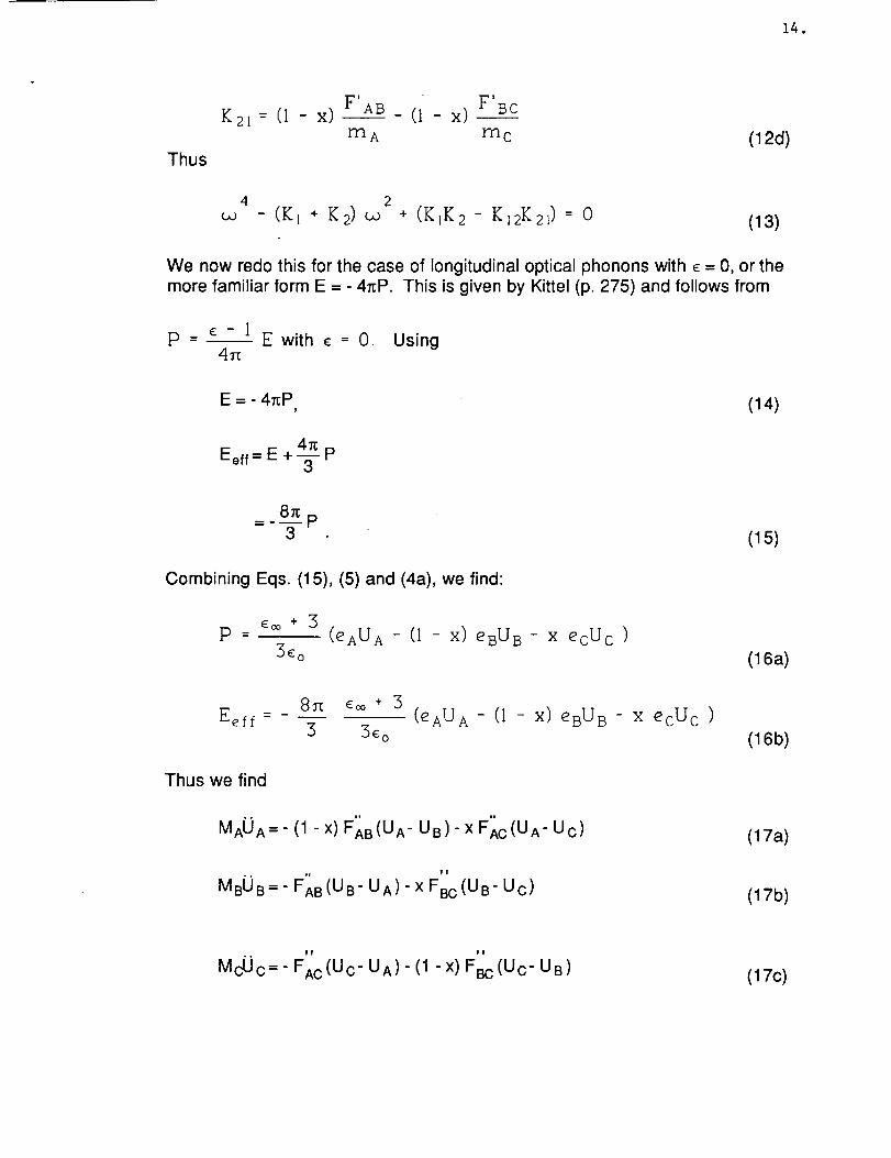
Thus
K21 = (l - x) F'A------_B-(i - X) F'BC
rrl A rl'l c (12d)
4 2- (K l + K 2) _ + (KIK 2 - K]2K21) = 0 (13)
We now redo this for the case of longitudinal optical phonons with e = 0, or themore familiar form E = - 47rP. This is given by Kittel (p. 275) and follows from
p _ c - 1 E with e = 0. Using4_
E=-47rP, (14)
Eef f = E + -_- P
8/_P
3 (15)
Combining Eqs. (15), (5) and (4a), we find:
eco+ 3P - (eAU A - (i - X) eBU B - x eoUc )
3e o (16a)
Eeff81"[ £o_ +
3 3e o(eAU A - (i - x) eBU B - x ecUc )
(16b)
Thus we find
MAOA=- (1 - X) FAB(U A- UB)- X FAc(U A- Uc) (17a)
MB0 B =- FAB (U B - UA)- X FBc (UB" Uc)(17b)
I! I!
McUc=- FAc(U c- UA)- (1 -x) FBC (U c- UB)(17c)

15.
where
= __ + 2)FAB'' FA B + 8rt N eAe B (.coo3 3coo
,, = __ (.coo+ 2)FA c FA C + 8_ IkleAe C3 3coo
(18a)
,, (coo+ 2FB 8_ M eBe C ).c = FBc- T 3coo
(18b)
(18c)
Thus we have the same equation for transverse and longitudinal optic phonons,
except that FAB replaces FAB.
We assume that N and Coodepend on x as follows:
N = (1 - x) NAB + x NAC
coo =(1 -X) coo, AB +xcoo ,AC
and we also assume
eB = eAB
e C = eAC
SO eA = (1 - X) eAB+ X eAC
where e* is the Szigeti effective charge.
(19a)
(19b)
(20a)
(20b)
(20c)
Now it is a matter of solving Eq. (13).
Summary for crystals of the form AB 1.xCx , we need to solve Eq. (13) for co 2 with
the K.'s defined by Eq. (12) in which the F' 's are replaced by F"'s with Eq.i
(20) used. The solution gives 00 2 as a function of x.
For the spherical case of long wavelength optical phonons at x = 0 and x - 1,we find the following initial conditions.
16.
X = O
2 FAB0 81"[°aL 0 AB
[tAB 3
* 2
2
°°gap, AB =
FAC O + FBC 0
Mc
x=l
2 FAC O (i - @) 8_°°L 0 AC = +
_AC 5(e*AC)2 ( )
NAC ,e_, A_C_+ 2
IJ.AC _ 3eoo, AC
2 FABO + Fmc° (1 - O)°°local, AC =
Ms
1__= 1 1 1 1 1where IJ,AB a_ + MBB and P-AC = MA + Mc"
There is also the question as to whether the two mode theory for photonscattering is the same as the two mode theory needed for electron scattering.One might say that the Green's function for scattering in the two cases would beclearly different. However we are interested in long wavelength modes mostly,and at any rate the Green's function probably depends more on frequency thanwave vector. Thus we assume our approximation is not a bad one. This isespecially true because we assume each optic mode only has one frequencywhich is independent of wave vector.
SELECTED REFERENCES
, M.P. Volz, F.R. Szofran, S.L. Lehoczky and Ching-Hua Su, "Lattice Vibration
Spectra of Hgl.xZnxTe Alloys," Solid State Communications75, 943-947
(1990).
. M. Gorska and W. Nazarewicz, "Application of the Random-Element
Isodisplacement Model to Long-Wavelength Optical Phonons in CdSexTelo x
Mixed Crystals," phys. stat. sol. (b) 65, 193 (1974).

17.
.
o
°
.
J. Baars and F. Sorger, "Restralen Spectra of HgTe and CdHgl.xTe," Solid
State Communications, Vol. 10, pp. 875-878, 1972.
I.F. Chang and S.S. Mitra, "Long Wavelength Optical Phonons in Mixed
Crystals," Adv. Phys. 20,359-404 (1971).
I.F. Chang and S.S. Mitra, "Application of a Modified Random-Element-Isodisplacement Model to Long-Wavelength Optic Phonons of Mixed Crystals,"Phys. Rev. 172, 924 (1968).
Y.S. Chen, W. Shockley, and G.L. Pearson, "Lattice Vibration Spectra of
GaAsx Pl-x Single Crystals," Phys. Rev. 151,648-656 (1966).
7. H.W. Verleur and A.S. Barker Jr., Phys. Rev. 149,715 (1966).

18.
In the following graph we plot MCT mobility versus temperature for several differentvalues of transverse charge which have appeared in the literature. The maindifference appears at intermediate temperature where variations of 10% or so can beseen. See also the accompanying table where numbers and references to the valuesof transverse charge are given. It seems clear that the effective charge determiningthe strength of scattering is not rigorously determined. However, different reasonablechoices seem to have little effect on the mobility vs. temperature.
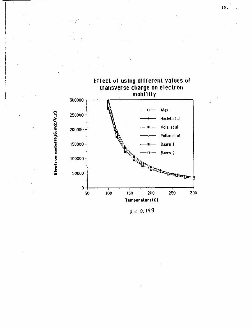
19°
ir.,
300000
250000
200000
150000
100000
50000
Effect of using different values oftransverse cl_arge on electron
11|oblllty
50 I00 150 200
Iempera|ure(K)
X = O. I_
25O 300

12,5456789
!0II1213141516
Iemp.
60.00080.000
100.000120.000140.000160.000180.000200.000220.000240.000260.000280.000300,000320.000340.000360,000
Alex. Hoclet.etal
75t076.988 784033.540474669.724 493102.113281514.659 295403,722180222.338. 190577.704128833.736 135450,2599824i.851. 104473.18577950.747 83773.96265094.544 69196,17454977.009 58386.93647153.305 50002.29640917.205 43317.08735825.421 '37869.65231590.175" 33362.54028069.279 29574.54025048.543 26373.16822488.594 23628,672
AUTHOR
Alex
Hoclet
Volz
Polian
Baars
eT/¢ (HgTe)
2.96
2.72
2.72
2.52
5.2
Volz, el.al Pollanel.al. baars ! Baars 2
7848241112 779743.921 745762.683 751620.406494049.558 504562.754 465220.325 475571,316296080.181 304674.154 271577.235 280418.237191046.739 197450.278 173138.017 180278.574135788.053 141634.843 122946.166 '128853.993104729.670 .... 108572.000 94170.610 .98234.53683976.153 87068.487 75207.492 77915.40169359.012 71893.737 62144.293 65077.60558520.214 60613.609 52537.899 54960.13250112,73t , 51862,702 45074.538" 47137.17543406.770 44867.309 39147,968 40902.063
'37947.938 39199.175 34318.862 35812.10933429,177 34496.583 30287.202 3157814229636.356 30549.166 26942.153 28058,859
26422,784 27225.t81 24088.784 25039.74423673.498 24365.650 21631.696 22480.530
eT/e(CdTe) REFERENCE
2.35 S.L. Lehoczky, F.R.
Szofran and B.G. Martin,
"Advanced Methods for Prep-aration and Characterization of
Infrared Detector Materials, PartI," NASA CR-161598, Page 70,July 5, 1980.
2.27 phys. stat. sol (b) 92,
545, (1979)
2.239 Solid State Comm.,
Vol. 75, No. 12, pp.943-947, 1990
2.38 Phys. Rev. B, Vol.13, Number 8, 1976
2,245 Solid State Communic.,
Vol 10, pp 875-878,1972
20.
Baars 2.981
* E®*2 *used e T - e s
3
2.287 Solid State Communic.,Vol. I0, pp. 875-878,
1972
Reference -*Lucovsky et aI., Phys.Rev. B, Vo!, 4, Number 4, 1367-1371, 1971.

21.
C. Review of Alloy Disorder Scattering
The alloy Hamiltonian can be written, in an approximation, as a uniform virtualHamiltonian with a residual alloy disorder potential. The virtual crystal approximationis used in alloys which are formed by ternary solid solutions between II-VI binarycompounds. In the virtual crystal approximation (VCA) the actual non periodicstructure is replaced by an average which is periodic. We consider a crystal of the
form AxBI.xC. The lattice of the atoms A is fcc and the lattice of the B, C atoms
randomly occupy a second fcc lattice. Thus in VCA, the random potential, created by
B(VB) and C(Vc) atoms is not used. Instead, a periodic potential which is the weighted
averages of these two is appropriate. In equation form, we write
<V> =V A + xV c + (1 - x)V B.
The use of the average potential leads again to Bloch waves and effective masses, butthe residual disorder then leads to scattering between the Bloch waves and to acompositional dependence of the band gaps. Only when the two binaries making upthe pseudobinary alloy have very similar band structure and lattices, does the bandgap vary approximately linearly with composition. After analysis, this typically leads toa scattering term proportional to x(1-x), however things are really not so simple as oneneeds to know with what strength to treat this scattering term. The answer that isusually given is that the strength is proportional to the difference between two bandwidths. For example in MCT, the difference in the bandwidth between HgTe and CdTe.Kossut has looked at the scattering in more detail and finds that it actually depends onthree matrix elements involving the difference in potential between Hg and Cd. The
one involving the spin-orbit interaction is apparently zero for MCT, the other two, arenot necessarily zero. Only when two of the three are zero is the scattering proportionalto the difference in the band gap energies from HgTe and CdTe. One further problem
is the non uniformity of the disorder via, for example, clustering.
SELECTED REFERENCES
. M.A. Berding, S. Krishnamurthy, and A. Sher, "Electronic and TransportProperties of HgCdTe and HgZnTe," J. Vac. Sci. Technol. 5A, 26-30 (1987).
. K.C. Hass, R.J. Lempert, and H. Ehrenreich, "Effects of Chemical and StructuralDisorder in Semiconducting Pseudobinary Alloys," Phys. Rev. Letters 52, 77-80
(1984).
. D.S. Montgomery, "Disorder Scattering and Electron Mobility in Hgl_xCdxTe,"
J. Phys. C • Solid State Physics 16,2923-2934 (1983).
, J. Kossut, "The Disorder Scattering in Zincblende Narrow-Gap SemiconductionMixed Crystals," phys. stat. sol. (b) 86,593 (1978).

22.
° L. Makowski and M. Glicksman, "Disorder Scattering in Solid Solutions of III-V
Semiconducting Compounds," 34,487-492 (1973).

23.
D. Other Scattering Mechanisms
Obviously dislocations are imperfections in the crystal and as such they can act asscattering centers. For example, edge dislocations create strain fields which canscatter electrons due to coupling to the deformation potential. Dislocations can alsobecome charged and thus act as scattering centers due to their charge which may bescreened by free carriers or impurities or both. A discussion of dislocation scatteringhas been given by Zawadzki. It should be pointed out that this subject is not only ofacademic interest. Pelliciari, Destefanis, and DiCioccio have found evidence of
anomalous behavior in low n type mercury cadmium telluride induced by extendeddefects. Their samples have shown a kink in the mobility curve between 77 and 100K. Transmission Electron Microscopy experiments have correlated this kink with the
appearance of dislocations and a significant decrease in the mobility. A very seriouspractical problem is the effect of temperature gradients on dislocation formation duringcrystal growth.
SELECTED REFERENCES
° B. Pelliciari, G.L. Destefanis, and L. DiCioccio, "Evidence of anomalous
behavior in low n-type mercury cadmium telluride induced by extendeddefects," J. Vac. Sci. Technol. A7 (2), 314-320 (1989).
. W. Zawadzki, "Mechanisms of Electron Scattering in Semiconductors,"Handbook on Semiconductors Vol. 1, Ch. 12 North-Holland Publ. co. (1982).

24.
E. Further Work in MZT
The best summary of further work on MZT that we have done has been summarized in
a recent paper by us which appeared in the August issue of the Journal of MaterialsResearch. One of the main results of thi_ paper is a comparison of our work with
experimental work done by others. We should also mention that although MZT hasseveral advantages as a IR detector (over MCT) primarily because of its increased Hg
stability it also suffers from a greater difficulty in growing uniform crystals. This is
dEgbecause less Zn than Cd is needed for a given E and dx for E's of interest is
ggreater for MZT. Thus small errors in x are magnified in energy gap fluctuations.
SELECTED REFERENCES
, J.D. Patterson, Wafaa A. Gobba, and S.L. Lehoczky, "Electron Mobility in n-Type
Hg 1-xCdx Te and Hg l_xZnxTe Alloys," J. Materials Research 7' (August 1992) to
be published.
. Wafaa Abdelhakiem and J.D. Patterson, "A comparison between electron
mobility in n-type Hgl.xCdxTe and Hgl_xZnxT," Materials Letters 11.47-51
(1991).
. E.A. Patten, M.H. Kalisher, G.R. Chapman, J.M. Fulton, C.Y. Huang. P.R. Norton,
M. Ray and S. Sen, "HgZnTe for very long wavelength infrared applications," J.Vac. Sci. Technol. B9(3), 1746-1751 (1991).
, G. Le Bastard, R. Granger, S. Rolland, Y. Marqueton, and R. Triboulet, "Optical
Vibration Models in Hgl.xZnxTeSolid Solutions near q = 0," J. Phys. France50
3223-3232 (1989).
. R. Granger and C.M. Pelletier, "Electron Mobility Evaluation in Hgl_xCdxTe and
Hgl_xZnxTe with Two Mode Optical Dispersion," Presented at 5th Int. Cong. on
II-Vi Compounds, Yokagama, Japan.
. S. Rolland, A. Lasbley, A. Seyni, R. Granger, and R. Triboulet, "ElectricalCharacterization of as-grown, annealed, and indium-doped Hgl_xZnxTe for x
near 0.15, "Revue Phys. Appl. 24, 795-802 (1989).
. R. Granger, A. Lasbley, S. Rolland, c.M. Pelletier, and R. Triboulet, "CarrierConcentration and Transport in Hgl.xZnxTe for x near 0.15," J. Crystal Growth
86,682-688 (1988).

25.
Fo Experimental Data
Experimental data on narrow gap materials other than MCT is relatively sparce.
Besides the references given in E we notethe papers by M. Voltz et al noted in B.
We have also "invented" some materia!sby_, changing the parameters of MZT and MCTby factors which are arbitrary but not totally unreasonable. The idea was to check if amore or less random but reasonable Set__ofparameters would fit experiment as well as
any. Happily they did not for otherwise we would have to say that our good resultswere fortuitous.
Other references include:
o S.D. Cobb, R.N. Andrews, F.R. Szofran, and SoL. Lehoczky, "Characterization of
Directionally Solidified MErcury Zinc Selenide Semiconducting Alloys," J. Cryst.
Growth 110 (3) 415-22 (1991).
1 K. Kumazaki, "Dielectric Constant of Zinc Mercury Selenide (ZnxHgl.xSe)
Determined by Raman Scattering," phys. stat. solids B, 160, K173-176 (1990).
. K. Kumazaki, "Resonant Raman Scattering in Zinc Mercury Selenide," phys.status solidi B 183,751-6 (1989).
, K. Kumazaki, L. Vina, C. Unbach, M. Cardona, "lnterband Critical Point
Parameters Determined by Ellipsometry in Zinc Mercury Selenide," Solid State
Commun. 68,591-4 (1988).
o K. Kumazaki, "Optical Damping Constants due to Free Carriers in Narrow Gap
Semiconductors," Solid State Commun. 64,567-7 (1987).
26. °
[]
!000000
000000
600000
400000
200000
0! • ! I
tO0 200 300
x-.134Nd=l.5el6Na=OEd-2.6eV
400
TemperaLure(K)
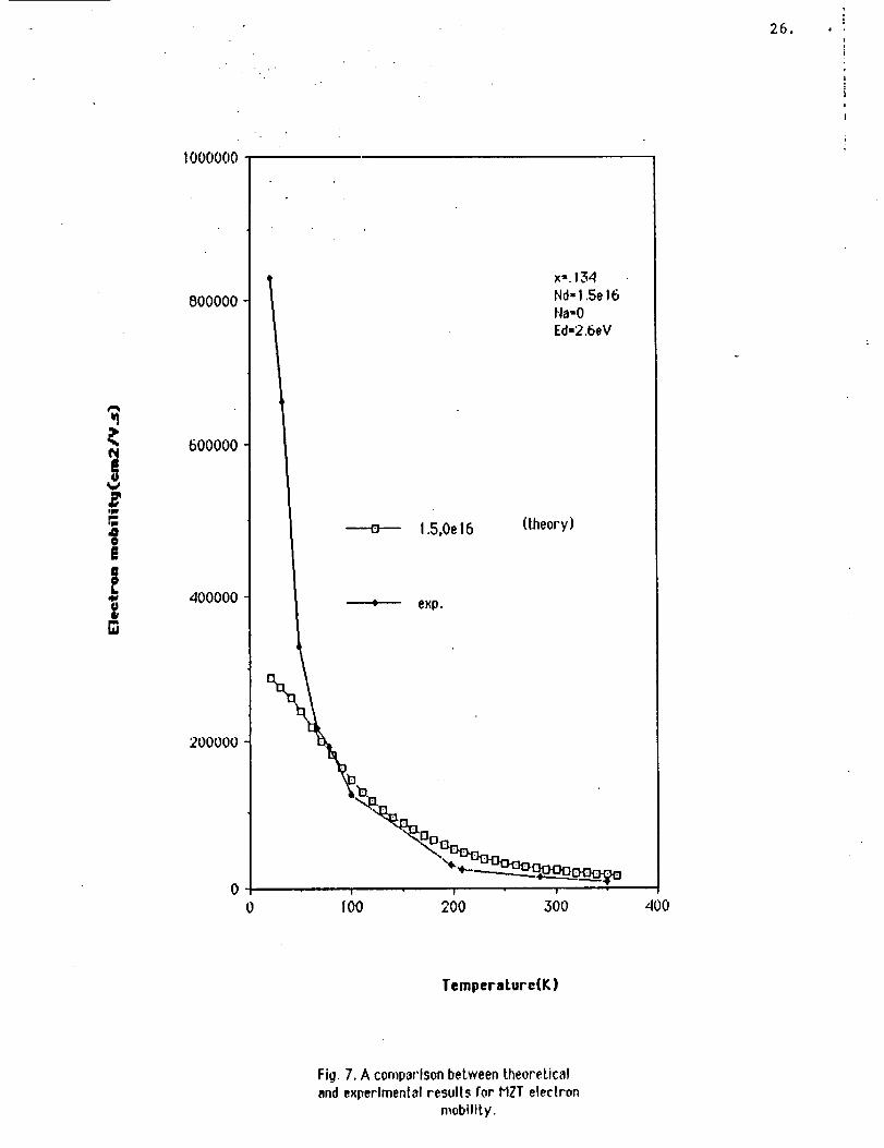
Fig. 7. A comparisonbetween theoreticaland experimental results for HZT electron
mobility,

27.
G. Superlattices
We have several comments to make about superlattices. Unfortunately experimental
studies require sophisticated equipment such as a molecular beam epitaxy apparatus.
A superlattice (SL) which has alternating layers of CdTe and HgTe has been proposedby Schulman and McGill as a new IR material which can be made by molecular beamepitaxy. The first successful molecular beam epitaxy growth of a Hg-Te superlattticeoccurred in 1982. The band gap depends on the width of the quantum wells as wellas the barrier width and height. Thus the formation of HgTe/CdTe superlattices allow agood control of the bandgap (in fact better than obtained in the growth of alloys) whichcan be a variable from zero to about 1.6 eV. We have also done some rough modeling
of high mobility devices which are based on doping in the barrier to furnish electronsto the quantum wells. Some results are given below. Representative references arelisted.
There are several comments one could make about the utility of superlattices as IRdetectors. In some ways superlattices are an advantage. For one, the energy gap
versus SL well layer thickness d wcan be better controlled in SL's than Eg versus x in
bulk crystals - at least for Eg'S of interest. This is particularly true because the cut off
wavelength for Eg'S of interest is a much more rapidly varying function of x for bulkcrystals than of the layer thickness for superlattices.
There exists a neat trick (Stormer and Dingle) in SL's that can be used to increase thenumber of electrons without reducing the low temperature mobility due to ionizedimpurity scattering. This is accomplished by adding donors to the barrier regionallowing the electrons to fall into the "wells". In calculations dealing with electronmobility in superlattices, it has been found that the temperature dependence of themobility is greatly affected by interface roughness which leads to complications inmaking accurate calculations.
There are other advantages to the HgTe-CdTe superlattices as given by Smith, McGill
and Schulman. The superlattice tunneling currents are reduced compared to bulk anddiffusion currents in photovoltaic devices made from SL's are reduced as is band toband tunneling currents across the junction.
HgTe-ZnTe SL's have also been considered but because of a 6.5% lattice mismatchthese become strained layer superlattices. The straining can cause additional effectswhich may be tailored to advantage. We have also done calculations which modelcrudely the way mobility can be enhanced by using layered structures consisting ofalternate layers of "quantum wells" and barriers.

28.
The electron wave function in superlattices is approximately (1);
A ik. r
* eA --, A
Vc_ (r) Xm(z ) if_ is in an A layer,
and
ik. r B B -"]3._,= _L, e VCk (r) Xm (z) if r is in a B layer,(r) c
where k is the direction perpendicular to the z direction (perpendicular to the layers),.,,&
AorB
Vc_ is the Bloch wave function for the A or B material, and Xm (z) is the envelope
wave function which is given by the Schroedinger equation"
2 2 ) AorB_ h. __8 + V c (z) Xm (Z) = Cm XmA or S
2m (Z) 8Z 2 (Z)
in a reasonable approximation.
Here, m* is the electron effective mass of the A or B material, Vc (z) is the energy level
of the bottom of the conduction bands and cm is the energy eigenvalue which
represents the confinement energy of the carriers. The boundary conditions at the
interfaces between A and B materials are that X (z) and [t/m* (z) ] [SX m (z)/Sz]m
be continuous. The energy levels in the conduction band can be approximated by the
Kane model for describing the electrons and holes in the A and B materials. Further
details are given in Bastard (2).
In general the question of energy bands in superlattices is very complicated. For onesituation, once can picture the parabolic quarter wells as splitting the original A or Bbands into mini bands. One of the most controversial items in band structure
determinations is the value of the valence band offset. There is also band bending
which can occur when charge is transferred between barriers and wells.

29.
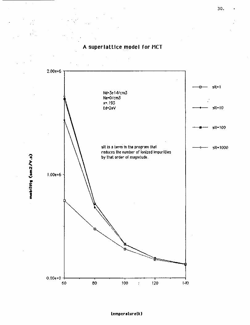
In the following graphs we have done a calculation which models very crudely the waythat mobility can be enhanced by using layered structures consisting of alternatelayers of quantum wells and barriers. If one adds donors in the barriers the resultingelectrons will drift to the quantum well resulting in more electrons without more
scattering centers. The actual calculation we have done keeps the number ofelectrons constant and reduces the number of scattering centers. Thus the low
temperature mobility (parallel to the layers) would be increased. In the followinggraphs sit = 10 means we have Nd electrons at low temperatures with only Nd/10
ionized impurities/volume. Further increase of sit to 100 produces minimal lowtemperature gain in the mobility. There is no change in the effect for further increasein sit which seems to mean that the effect "saturates" for high electron concentration atlow temperature. This would mean that ii impurity scattering has become negligibledue to a decrease in ii scattering centers.
30°
A superlattlce model for MCT
2.00e+6
;=
|
1.00e+6
O.OOe+O
60
Nd=3e14/cm3Na,,O/cm3x-.193Ed-2eV
sit is a term in the program thatreduces the numberof"Ionizedimpuritiesby that order ofmagnitude.
! ! I
80 100 : 120 14'
lm
slt-I
_It-10
slt-lO0
slt-IO00
temperature(k)

31. •
A superlattlce model for MZT
I
QO
1.50e+6
I.OOe+6
500e+5
0.00e+0
6O
\
Nd=3e14/cm3Na-OEd=2.6eVx-.1315
sit Is a term In the program thatreduces [he number of ionized impurities
b.ythat order of magnitude.
! I I
80 I00 120
ii
4O
Slt.'=I
slt=lO
slt=lO0
slt.--lO00
temperature(k}

32.
SELECTED REFERENCES
o C. Weisbuch and B. Vinter, "Quantum Semiconductor Structures," Academic
Press, Inc., New York, 1991.
. J.R. Meyer, D.J. Arnold, C.A. Hoffman, and F.J. Bartoli, "Theory for Electron andHole Transport in HgTe-CdTeSuperlattices," J. Vac. Sci. Technol. B9(3), 1818-
1822 (1991).
. G. Bastard, J.A. Brun, and R. Ferreira, "Electronic States in SemiconductorHeterostructures" in Solid State Physics Editors Henry Ehrenreich and DavidTurnbull 44, 229-415 (1991).
, G. Bastard, "Wave Mechanics Applied to Semiconductor Heterostructures,"Halsted Press, New York, 1988.
. Jean-Pierre Faurie, "Growth and Properties of HgTe-CdTe and Other Hg-Based
Superlattices," IEEE Journal of Quantum Electronics, VoI. QE-22(9) 1656-1665
(1986).
, D.L. Smith, T.C. McGill and J.N. Schulman, "Advantages of the HgTe-CdTe
Superlattice as an Infrared Detector Material," Appl. Phys. Lett. 43 (2), 180-182(1983).
° J.N. Schulman and T.C. McGill, 'qhe CdTe/HgTe Superlattice:Proposal for a New Infrared Material Appl. Phys. Lett. 34 (10), 663-665 (1979).
33.
H. MMT and Parameter Tables
A preprint of a paper is enclosed which has the parameter tables for MMT and
also the results of our mobility calculations.

34.
A comparison between electron mobilitles in Hgl.xMnxTe and
Hgl -x C d x T e °
Wafaa A. Gobba and J. D. Patterson
Department of Physics and Space Sciences
Florida Institute of Technology
Melbourne, FL 32901-6988 U.S.A
and
S. L. Lehoczky
ES75, Space Science Laboratory
Marshall Space Flight Center, AL 35812 U.S.A.
3.5.
ABSTRACT
Electron mobility in the n-type diluted magnetic semiconductor
Hgl.xMnxTe has been calculated in the absence of a magnetic field.
The results were compared to those of Hgl.xCdxTe for the same range of
energy gap. The calculations are based on solving the Boltzman equation
using a variational principles technique. The scattering processes that
are included in the calculations are the scattering of the electrons with
the ionizied impurities, holes, alloy disorder, acoustic phonons and
longitudinal optical phonons. At room temperatures the mobilities are
nearly the same, while at temperatures of order of liquid nitrogen they
are about 30% less for MMT as compared to MCT with the same
concentration of defects. Hgl.xMnxTe represents a good material for
infrared detectors. One of the advantages it has over Hgl-xCdxTe is that
the band gap changes faster with Mn in Hgl-xMnxTe than it does with Cd in
Hgl.xCdxTe which leads to less scattering due to alloy disorder.
36.
I. Introduction
Although Hgl-xCdxTe (MCT) has many problems due to lattice,
surface, and interface instabilities(I) it is still a dominant material for
use in infrared detectors. Because of the disadvantages of MCT other
materials are being studied as better alternatives. One may start the
search for new materials by noting that Cd, Zn, Mg and Mn open the band
gap of the semimetals HgTe and HgSe(2) and thus produce potential
infrared detector materials. Hgl.xZnxTe may be superior for use as an
infrared detector over Hgl.xCdxTe because it is chemically more stable
and at the same time shares the same electronic properties(3-7). Hgl.
xCdxSe typically shows n-type conductance and does not easily show type
conversion(8). Mg has a stability problem with the Hg-Te bond when the
required amount for the 101_m range is introduced(9). Hgl_xMnxTe (MMT) is
not a true II-VI alloy but it acts as one. The 3d orbitals of Mn are exactly
filled with one electron per orbital and the five spins in these orbitals are
parallel, by Hund's rule. It would require about 6-7 eV to add an addition
electron with opposite spin to the Mn atom. As a result the 3d5 shell acts
as if it is complete shell and the Mn atom behaves as a group II
element(lo).
MMT being a diluted magnetic semiconductor, represents a good
material for infrared detectors for the following reasons :
1) Cd_.xMnxTe provides a suitable substrate for epitaxial growth due to
its lattice constant(11).
2) The band gap changes approximately twice as fast with Mn in MMT as
with Cd in MCT. A smaller amount of Mn is needed to produce the same
required energy gap which leads to less scattering due to alloydisorder(_2). For detection in the 8-14/Jm window 20% CdTe in MCT
is needed while only about 11% MnTe in MMT is required.
3) Using a magnetic field, at very low temperatures, the energy gap can
be fine tuned due to the presence of the exchange interaction(_3).
4) Lattice, surface and interface instabilities(_4) in MMT are less when
compared to MCT due to the bond stability of Hg-Te.
5) Segregation(15,16) of CdTe in MCT is more of a problem than segregationof MnTe in MMT. Thus MMT is more uniform.

37.
Diluted magnetic semiconductors (DMS) are characterized by the
presence of substitutional magnetic ions which causes spin-spin exchange
interactions between the localized magnetic moments and the band
electrons. This interaction changes the band structure and the impurity
states in the presence of a magnetic field. The significance of this
interaction has been explained in several review articles(17-21).
Single crystals of MMT have been grown using different techniques:
the Bridgman method(22-24), the travelling-solvent method(25), the liquid-
phase epitaxy method (LPE(26)), the two phase liquid method(27)and the
isothermal vapor-phase epitaxy method (VPE(28)). The as grown
crystals(29) of MMT and MCT are often p-type due to Hg vacancies. By
annealing(30) the samples for a certain time in Hg vapor at low
temperature they can be converted to n type. Delves(31) in 1965 started
the work on semimagnetic semiconducting single crystals which Holm(23)
and Furdyna and Leibler(32) et al. continued. Much of this research as well
as work of more recent vintage, has been reviewed by Furdyna(33,34). A
thorough review of MMT with more than 150 references has been given
by Rogalski(2).
Because MMT is paramagnetic, has the ZnS structure for all
compositions at least up to x ___-0.35, and because of many other
similarities, Johnson(29) et al. assumed that in the absence of an applied
magnetic field the physical properties of MMT for x <0.35 are similar to
those of MCT. This assumption was made based on the work of Furdyna(30)
who mentioned in his paper that mobilities ofP 10 S= cm2/V.s or more
were observed at 77K. However, there have not yet been electron mobility
calculations for MMT which could be cOmpared to MCT. The purpose of this
paper is to collect the required band and material parameters and do the
mobility calculations. Most of the parameters are obtained from
experiment. They will be combined with a calculational model already
used for MCT and MZT, transport properties of MMT in the absence of a
magnetic field will be obtained, and the results will be compared with
those of MCT for the same energy gap.
Since the band structure of MMT in the absence of a magnetic field
does not show any effects caused by the magnetic ions it can be described
by Kane's theory(35,36). Under this condition the procedure of calculating
the electron mobility in n-type MMT and the concentration of the free
carriers would be the same as in our previous calculations of MZT(3,4,37).
-: 38.
; i
'A
_ gi
An outline of the model used is given in section II, values of the band
and material parameters extracted from experiments are given in section
III, calculations and results are given in section IV and finally conclusions
are given in section V.
II Theory:
As was mentioned before the wave functions of the conduction
electrons and the dispersion relation are described by the Kane three band
model(3) in the absence of a magnetic field. The non-parabolicity of the
energy band has been considered. Due to the high ionicity of the material
and the importance of the optical phonon interaction, the relaxation time
approximation could not be used and a numerical technique has to be used
in solving the Boltzman equation. In setting up the Boltzmann equation,
the interaction of the electrons with the ionized impurities, heavy holes,
alloy disorder, acoustic phonons and polar optical phonons were
considered. At low temperature the scattering is mainly due to ionized
impurities. The charged impurity atoms do not scatter high energy
electrons and this scattering process decreases with increasing
temperature. Optical phonon scattering is predominant at high
temperature and the Frolich perturbation potential is used to describe the
interaction. For acoustic phonons, the deformation potential which arises
from the changes in the energy band gap as a result of the changes in the
spacing of the lattice atoms is used. In mixed alloys, like MMT, Hg and Mn
are randomly distributed in the crystal. Since a virtual crystal is
assumed for band structure purposes, the disorder in the crystal is taken
care of by the scattering of electrons from the alloy disorder. The details
of the calculations of each scattering mechanism, the model used for the
donor levels, the neutrality equation and the variational principles
technique used in solving the Boltzmann equation are given in (3, 37, 38-
42). Screening effects are included in the interaction with ionized
impurities, holes and optical phonons.
Since MMT contains the magnetic ions Mn**, the total electronic
Hamiltonian(3O) is given by
H = Ho + Hex= _ + _,J(r - _)Sj. _, (1)R,
where Ho is the Hamiltonian term for a nonmagnetic semiconductor, H,,x is
39
the term which takes care of the exchange interaction of the band
electrons with the localized magnetic moments, S_ and o-are the spin
operators of Mn** and of the band electron, respectively, J is the electron-
ion exchange coupling constant, and r and Rj are the band electron and
Mn.+ coordinates, respectively. The summation is taken over all the
lattice sites occupied by Mn.+ ions. Furdyna(3O) pointed out that since the
electronic wave function is very extended, the electron encounters many
Mn** ions at any time and Si could be replaced by the thermal average.-)
< S > of the Mn÷. spin of all ions. For a magnetic field in the z direction•-) A
and in the paramagnetic phase < S > can be replaced be < S. > k. Thus,
also using the virtual crystal approximation,
-'R),H,, = _, < S, > x__,Jtr- (2)
R
where the sum now runs over all sites. < S, > is proportional to the
magnetization which vanishes in the absence of an external field for a
paramagnet. It is then clear from equation (2) that the exchange term will
also vanish in the absence of a magnetic field, at least in the
paramagnetic phase. MMT is paramagentic(3O) at the composition and
temperature we are interested in.
III. Parameters for electron mobility and charge carrier
concentration calculation for Hgl.xMnxTe :
Mercury telluride crystallizes in the zinc blende type structure with
a lattice constant a = 6.461A °, while manganese telluride crystallizes
in the hexagonal NiAs type structure with lattice constants(43)a = 4.15 A °
and c = 6.71 A ° X-ray measurements and differential thermal analysis
were performed by Delves and Lewis(44) for the HgTe-MnTe system and the
following three phases were observed in the solid solution: (1) o_ phase
with the zinc blende type structure (0 < x < 0.36), (2) cz phase plus MnTe2
with the pyrite structure (0.36< x <0.75), and (3) MnTe with NiAs type
structure (x > 0.75). For x" < 0.36, Hgl.xMnxTe crystal growth behaviour is
very similar to that of Hgl.xCdxTe for comparable(2)x. For _" > 0.36, Hgl-
xMnxTe has more than one crystallographic phase which makes the
material not favorable for devices applications.
The energy gap in MMT behaves in the same manner as in the MCT. It
changes from a negative band gap semimetal to a positive band gap
semiconductor as the composition x, (which gives the concentration of Mn

40.
in MMT or Cd in MCT), increases from zero. A zero band gap is achieved at
4.2K temperature(29), when x=0.07 in MMT and when x=0.15 for MCT. The
change in MMT energy gap with x is twice as fast as it is in MCT(3O). The
equation deduced from experiments for the energy gap ( C6-/-'8 ) as a
function of those two terms has been given by Kaniewksi and Mycielski(45),
_(x, T) =-0.253+3.446x +4.9 .10-4"/" -2.55*10-3xT (eV).
The Kane momentum matrix element was obtained from interband
magnetooptics experiments (46,47) and it is a function of the
composition(48) x, P(x)=(8.35-7.94x) x lO-seVcm.
Gebicki and Nazarewicz(,9) measured the infrared reflection spectra
in the optical region from 50 to 300 cm-1 at 90 and 295 K of MMT with
0 < x < 0.69. These crystals were grown by the Bridgman method and
their crystallographic structure was tested by X-ray diffraction to ensure
they have the zincblende structure. They obtained the dielectric functions
versus wave number by applying the Kramers-Kronig analysis to the
reflection spectra. The position of the maxima of Ime (co) and
Irn(-1/e(co)) indicate the long-wavelength phonon frequencies for
transverse and longitudinal optical phonons respectively. For each value
of x, two frequencies of the transverse optical phonons and two of the
longitudinal optical phonons were found as is consistent with "two-mode"
behaviour" of the phonon spectra. They calculated the long-wavelength
optical phonon frequencies as a function of composition using the random-
element isodisplacement (REI) model (5o,51)which is applicable only for
the composition range at which the crystal structure does not change. For
this reason the unknown parameters of the REI model were determined
from the optical phonon frequencies for x = 0 (HgTe) and x = 0.69. The x =
1 (MnTe) data cannot be used because the change of the crystal structure
causes discontinuity of the phonon spectra. When they compared their
theoretical results for the composition range 0 < x ___0.69 with
experiment they obtained good agreement. Using their results for the
dependence of long-wavelength optical phonon frequencies on composition
we extracted the frequency equations we needed for our model using
linear interpolation between the points x = 0 and x = 0.4 (where the curve
was linear). We obtained:
rOLo(HgTe ) = 1 34 - 5x, ro_(HgTe) = 1 1 0 + 27.5x
_Lo(MnTe) = 1 87+ 25x, coTo(MnTe) = 1 87- 5x
I
The Callen effective charge, e_., which is related to the relative
displacements of atoms in a unit cell, determines the strength of the
interaction of the electrons with the LO-phonon (see reference 39, page
80). The Szigeti effective charge,e;, and the total transverse charge are
related to the Callen effective charge by the relations:
e;,= + 21e" =L 3e_ J s and e'_ eTE-.In reference (51), Gorska et al. made the assumption that the charges eB
and ec in the REI theoretical model are the Szigeti effective charges
e,,= eo= e',,c.W. Gbicki et a1.(49), in their calculation of optical phonons in MMT
took the effective charge of all ions to be equal to that of HgTe(42)
eA/e = eB/e = ec/e = 0.6
Using these equations and the values mentioned earlier for the dielectric
constants for HgTe and MnTe, the transverse charges are:
_(HgTe) = 3.44, _(MnTe)=3.32
The parameters needed for the interaction of the electrons with the
acoustic phonons are the longitudinal and transverse sound velocities and
the deformation potentials(42). The longitudinal and transverse acoustic
waves has the simple relations(s2), vl=J_ --J and v,=-q/"p 4 Because
of the lack of measurements done on MnTe and due to the fact that the Mn
portion is very small, we assume the Mn causes a negligible change in vl
and vt. Using the longitudinal and transverse sound velocities(S2) of HgTe,
Cll = 5.361 x 10¹¹ dyne/cm2, 044 = 2.123 dyne/cm2 and the density (2) of
HgTe = 8.076 (gm/cm3), the longitudinal and transverse velocities can
easily be estimated. We obtain vl = 2.576 x 105 cm/sec and vt = 1.621 x
105 cm/sec.
For MMT a virtual crystal was assumed and the band structure was
described by the Kane theory. The compositional disorder is considered in
the scattering of the electrons, tt is treated as a random distribution of
square-well scattering centers with dimensions of a unit cell and with a
depth approximately equal to the difference between the band gaps of the
end-point compounds(38). Using the Energy gap(2) values at 4.2KO of HgTe
and MnTe when they both have the zinc blende structure we got a value of

42.
3.5eV for the disorder energy (Edis). These results as well as values for
all other needed quantities are summarized in Table (1).
IV. Calculations and Results:
MCT and MMT are compared for two different values of MMT enrgy
gap. The first value of MMT energy gap, x (MMT) = 0.0923, is chosen to give
values of the MMT energy gap that are very close to those of MCT, with
x(MCT) = 0.193, at low temperature (see fig. 1). This value was chosen as
typical for energy gaps appropriate to the 10/_m window. Other
appropriate values of x can be used with equal facility in our mobility
calculations. The second value of MMT energy gap, x(MMT) = 0.094, is
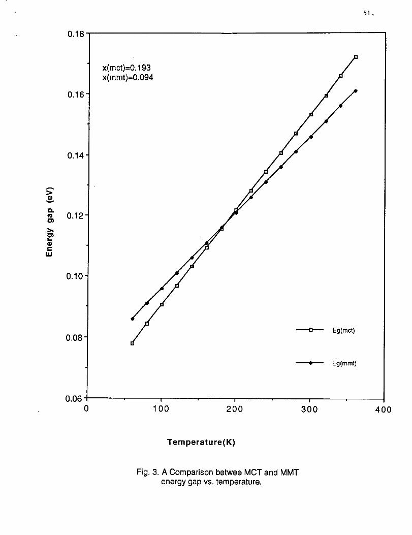
chosen to give values of the MMT energy gap that agrees with those of MCT
with x = 0.193 at intermediate temperature (see fig. 3). In both cases we
used a donor concentration equal to Nd = 3 x 10¹⁴ /cm3 and acceptor
concentration equal to Na = 0. In each case we considered two kinds of
donors, one kind is ionized with an energy which merges with the
conduction band and a concentration chosen so that Nd - Na is equal to the
concentration of electrons in MCT at very low temperature(4o). The second
kind are bound donors with a concentration and ionization energy chosen to
fit the concentration of the electrons vs temperature at low temperature
for MCT(4O). For the concentrations considered, the second donor had very
little effect. When the electron mobility in both cases were calculated
and compared they came out to be very close (see graphs 2 and 4) at high
temperatures but differed by about 30% at liquid nitrogen temperatures.
When another value of the MMT disorder energy, 1.8eV, was used the
mobility value was increased by approximately 25% over the whole range
of temperature.
V. Conclusions
Since MMT shares the same electronic properties as MCT for the
same energy gap and since it has the advantages that were mentioned
earlier, it is another strong candidate for use in infrared detectors.
However, Brimrose apparently continues to be the only company which
makes MMT detectors commercially. The possibility of varying the
electronic properties of MMT by use of a magnetic field makes MMT a very
intertesting material. The effects of this on the mobility await further
study.

43.
References
* Research supported by NASA/Marshall Space Flight Center, Grant
No. NAG8-781, Supplement 2.
1) W. E. Spicer, J. A. Silberman, I. Lindau, A. B. Chen, A. Sher and J. A.
Wilson, J. Vac. Sci. Technol. A1, 1735 (1983).
2) Antoni Rogalski, Infrared Phys., 3_!, No. 2, pp. 117-166 (1991).
3) Wafaa Abdelhakiem Gobba, "Theory of electron mobility in narrow-
gap semiconductors", Ph. D thesis, Florida Institute of Technology,
(1991).
4) Wafaa Abdelhakiem, J. D. Patterson and S. L. Lehoczky, Materials letters
11(12), 47-51 (1991).
5) A. Sher, A. B. Chen, W. E. Spicer and C. K. Shih, J. Vacuum Sci. Technol.
A3 , 105 (1985).
6) W. A. Harrison, J. Vacuum Sci. Technol. A1, 1672 (1983).
7) A. B. Chen, A. Sher and W. E. Spicer, J. Vacuum Sci. Technol. A1,1674
(1983).
8) N. P. Gavaleschko, P. N. Gorlei and V. A. Schendirovski, Uzkozonnye
poluprovodniki. Poluchenie i Fizicheskije Svojstva. Naukova
Dumka, Kiev (1984).
9) R. Tirboulet, M. Bourdillot, A. Durand and T. Nguyen Duy, Proc. SPIE
1106, 40 (1989).
10) K. C. Hass and H. Ehrenreich, J. Crystal growth 86, 8 (1988).
11) P. Becla, P. A. Wolff, R. L. Aggarwal and S. Y. Yuen, J. Vac. Sci. Technol.
A._3.3,116 (1985).
12) R. R. Galazka, J. Cryst. Growth 7._.22,364 (1985).
13) S. Wong and P. Becla, J. Vac. Sci. Technol. A...44,2019 (1986).
14) A. Wall, C. Caprile, A. Franciosi, R. Reifenberger and U. Debska, J. Vac.
Sci. Technol. A4. 818 (1986).
15) V. I. Kalenik, I. N. Gorbatiuk, I. M. Rarenko, O. A. Bodnaruk, O. D.
Pustylnik, S. E. Ostapov, V. P. Schafraniuk and A. F. Slonecki, in
Impurity and Defects of Narrow Gap semiconductors, Proc. 2nd AU-Union
Symp. Povlodar, Part 1, p. 87 (1989) (in Russian).
16) Infrared Products Brimrose Corporation, 5020 Campbell Blvd,
Baltimore, MD p. I-4. A brochure from this company.
17) R. R. Galazka, in Proceedings of the 14th International Conference on
the Conductors, Edinburgh, 1978, edited by B. L. H. Wilson (lOP, London,
1978), p. 133.
18) R. R. Galazka and J. Kossut, in Narrow Gap semiconductors: Physics
44.
and Applications, Vol. 133 of Lecture Notes in Physics, edited by W.
Zawadki (Springer, Berlin, 1980), p. 245.
19) J. A. Gaj, in Proceedings of the 15th International Conference on the
Physics of Semiconductors, Kyoto, 1980 [J. Phys. Soc. Jpn. Suppl. A49,
747 (1980)].
20) T. Dietl, Physics in High Magnetic Field, Vol. 24 of Springer Series
on Solid State Sciences, edited by S. Chikazumi and N. Miura (Springer,
Berlin, 1981), p. 344.
21) J. K. Furdyna, J. Appl. Phys.53, 7637 (1982).
22) R. T. Delves, Br. J. Appl. Phys. 16, 343 (1965).
23) R. T. Holm and J. K. Furdyna, Phys. Rev. B15, 844 (1977).
24) P. Becla, D. Heiman, J. Misiewicz, P. A. Wolff and D. Kaiser, SPIE
796, 108 (1987).
25) R. Triboulet, D. Triboulet and G. Didier, J. Crystal Growth 38, 82
(1977).
26) U. Debska, M. Dietl, G. Grabecki, E. Janik, E. Kierzek-Pecold and M.
Klimkiewicz, Physica Status Solidi 64a, 707 (1981).
27) I. E. Lopatynski, Inorg. Mater. 12, 296 (1976).
28) P. Becla, J. Lagowski, H. C. Gatos and L. Jedral, J. Electrochem. Soc.
129, 2855 (1982).
29) W. B. Johnson and J. R. Anderson, Phys. Rev. B 29(12), 6679(1984).
30) J. K. Furdyna, J. Vac. Sci. Technol., 21(1), 220 (1982).
31) R. T. Delves, Br. J. Appl. Phys. 16, 343 (1965).
32) K. Leibler, W. Giriat, Z. Wilamowski, and R. Iwanowski, Phys. Status
Solidi B47, 405 (1971).
33) J. K. Furdyna, J. appl. Phys. 64, R29 (1988).
34) R. K. Willardson and A. C. Beer (Treatise Eds), Semiconductors and
Semimetals, Vol. 25 (Volume edited by J. K. Furdyna and J. Kossut).
Academic, Boston (1988).
35) M. Jaczynski, J. Kossut, and R.R. Galazka, phys. stat. sol. (b) 88, 73
(1978).
36) Evan O. Kane, J. Phys. Chem. Solids 1, 249-261 (1957).
37) J.D. Patterson, Wafaa A. Gobba and S.L. Lehoczky,"Electron mobility
in n-type Hgl.xCdxTe and Hgl.xZnxTe allos", J. of Materials Research,
to be published, August 1992.
38) D. A. Nelson, J. G. Broerman, C. J. Summers, and C. R. Whitset, Phys.
Rev. B18 (4), 1658-1672 (1978).
39) S. L. Lehoczky, F. R. Szofran, and B. G. Martin, NASA CR-161598,
"Advanced Methods for preparation and Charactrization of Infrared
Detector Materials, Part I", July 5, 1980.

45.
40) S. L. Lehoczky, C. J. Summers, F. R. Szofran, and B. G. Martin, in
Materials Processing in the reduced Gravity Environment of Space,
Guy E. Rindone, Ed., Elsevier, Amsterdam, 1982, pp. 421-431.
41) S. L. Lehoczky, F. R. Szofran, in Materials Processing in the Reduced
Gravity Environment of Space, Guy E. Rindone, Ed., Elsevier,
Amsterdam, 1982, pp. 409-420.
42) S. L. Lehoczky, J. G. Broerman, Donald A. Nelson, and Charles R. Whitset,
Phys. Rev. B9, 1598-1620 (1974).
43) W. Giriat and J. K. Furdyna, Semiconductors and Semimetals, Vol. 25
(Edited by R. K. Willardson and A. C. Beer), p.l. Academic, Boston
(1988).
44) R. T. Delves and B. Lewis, J. Phys. Chem. Solids 24, 549 (1963).
45) J. Kaniewski and A. Mycielski, Solid St. Commun. 41, 959 (1982).
46) E. Janik and G. Karczewski, J. Electron. Mat. 16, 381 (1987).
47) G. Bastard, C. Rigaux, Y. Guldner, A. Mycielski, J. K. Furdyna
and D. P. Mullin, Phy. Rev. B24, 1961 (1981).
48) R. R. Galazka and J. Kossut, Londolt-B(_rnstein, New Series
17b, (Edited by O. Madelung, M. Schulz and M. Weiss), p. 302.
Springer, Berlin (1982).
49) W. Gebicki and W. Nazarewicz, Phys. Stat. Sol. (b) 80, 307 (1977).
50) H. Harada and S. Narita, J. Phys. Soc. Japan 30, 1628 (1971).
51) M. Gorska and W. Nazarewicz, Phys. Star. Sol. (b) 65, 193 (1974).
52) Karl W. Boer, Survey of Semiconductor Physics: Electrons and other
particles in bulksemiconductors, Van Nostrand Reinhold, p. 79-83.
53) D.L.Rode, Phys. Rev. B2, 4036 (1970).
54) A. Jedrzejczak and Dietl, Phys. Stat. Sol. 76b, 737 (1976).
46.
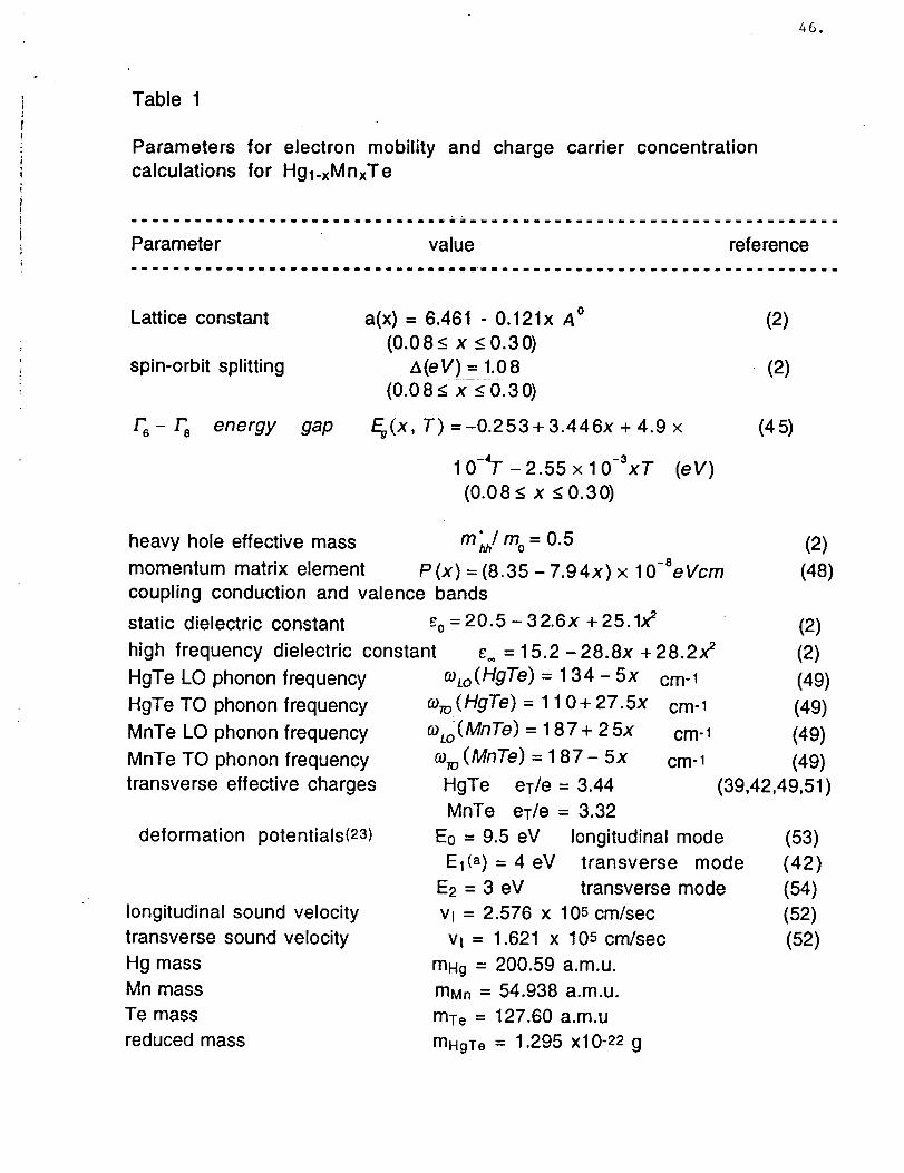
Table 1
Parameters for electron mobility and charge carrier concentration
calculations for Hgl-xMnxTe
............................. •. ,.,.__ ,, L .................................
Parameter value reference
Lattice constant
spin-orbit splitting
- T'e energy gap
a(x) = 6.461 - 0.121x A (2)
(0.08_< x _<0.30)
A(eV) = 1.08 (2)
(0.08< x <0.30)
_(x, T) =-0.253+ 3.446x + 4.9 x (45)
1 0-4T - 2.55 x 10⁻³xT (eV)
(0.08 < x -<0.30)
heavy hole effective mass m'J mo = 0.5
momentum matrix element P(x)=(8.35-7.94x)x lO-eeVcm
coupling conduction and valence bands
static dielectric constant _o = 20.5 - 32.6x + 25. lx 2
high frequency dielectric constant _.. = 15.2 - 28.8x + 28.2x 2
HgTe LO phonon frequency
HgTe TO phonon frequency
MnTe LO phonon frequency
MnTe TO phonon frequency
transverse effective charges
deformation potentials(23)
longitudinal sound velocity
transverse sound velocity
Hg mass
Mn mass
Te mass
reduced mass
OOLo(HgTe ) = 1 34 - 5x cm-1
c%(HgTe) = 110+27.5x cm-1
O_Lo(MnTe) = 187+ 25x cm-1
OOTO(MnTe) = 1 87- 5x cm-1
HgTe eT/e = 3.44
MnTe eT/e = 3.32
Eo = 9.5 eV longitudinal mode
E1 (a) = 4 eV transverse mode
E2 = 3 eV transverse mode
vi- 2.576 x 105 cm/sec
vt = 1.621 x 105 cm/sec
mHg = 200.59 a.m.u.
mMn = 54.938 a.m.u.
mTe = 127.60 a.m.u
mHgTe = 1.295 X10⁻²² g
(2)
(48)
(2)
(2)
(49)
(49)
(49)
(49)
(39,42,49,51)
(53)
(42)
(54)(52)(52)

47.
disorder energy
mMnTe = 0.615 X 10⁻²²g
Edis = 3.5eV (2),(38)
........................................... ,.,_,&=.= ............. _ ......
a) using hydrogenic approximation

48.
List of Figures
Fig. 1. A comparison between MCT and MMT energy gap vs. temperature.
Fig. 2. A comparison between MCT and MMT electron mobility vs.
temperature.
Fig. 3. A comparison between MCT and MMT energy gap vs. temperature.
Fig. 4. A comparison between MCT and MMT electron mobility vs.
temperature.

49.
A
C3.
[3)
>,,
L_
CIJJ
0.18
0.16
0.14
0.12
0.10
0.08
0.06
0
x(MCT)=0.193x(MMT)=0.0923
I • I
100 200
Eg(mct)
• Eg(mmt)
I
300 400
Temperature(K)
Fig. 1. A comparison between MCT and MMT
energy gap vs. temperature.

50.
A
o,IE
J_0
c0
8e+5
6e+5
4e+5
2e+5
Oe+O I I I
MCT
I MMT
Nd=3e14/cm3Na=0/cm3
x(MCT)=0.193x(MMT)=0.0923Ed(MCT)=2eVEd(MMT)= 3.5eV
0 100 200 300 400
Temperature (K)
Fig. 2. A comparison between MCT and MMT
electron mobility vs. temperature
51.
A
ov
Q.
¢=U.I
0.18
0.16
0.14
0.12
0.10
0.08
0.060
x(mct)=0.193x(mmt)=0.094
!
I00
I
200
Eg(mct)
- Eg(mmt)v
! |
300 400
Temperature(K)
Fig. 3. A Comparison betwee MCT and MMT
energy gap vs. temperature.

52.
A
Eu
mmm
0
c0i--
om
i,i
8e+5
6e+5
4e+5
2e+5
0e+00
!
100
!
200
mob(mct)
mob(mint,3.5)
x(mct)=.193x(mmt)=.094Ed(mct)=2eV
Ed(mmt)=3.5eVNd=3e14/cm3Na=0/cm3
I
300 40O
Temperature(K)
Fig. 4. A Comparison between MCT and MMTelectron mobility vs. temperature.

53.
I. References
We have given above a few particularly relevant references for each topic. Anextensive list of references has been computerized by us. We have listed it by topicsin the appendix.

_54.
J. Availability of Program
We have the program written in Fortran, and stored on a Sun, a Vax and a Nighthawk.However, because we have local networks as well as Internet, we can move theprogram around easily from computer to computer (on campus, in state or even out ofstate). Thus we could send our program or results to a properly networked terminal atMarshall Space Flight Center. The programs for MCT, MZT and MMT are alsoavailable on disks that are available as required.
55.
II.
1.
.
.
.
°
.
.
.
.
LIST OF REPORTS AND DOCUMENTS
James D. Patterson, Further Improvements in Program to Calculate ElectronicProperties of Narrow Band Gap Materials, Semi-Annual Report, NAG8-781Supplement 2, December 15, 1991.
Wafaa M.K.A. Gobba, 'q'heory of Electron Mobility in Narrow GapSemiconductors," Ph.D. Thesis, Florida Institute of Technology, August 1991.
J.D. Patterson, Wafaa A. Gobba, and S.L. Lehoczky, "Electron Mobility in n-typeHgCdTe and HgZnTe Alloys," To be published in the Journal of MaterialsScience.
J.D. Patterson and Wafaa A. Gobba, "The Physics of Astronomical InfraredDetectors," I.A.P.P.P. Communications47, 1-16 (1992).
Wafaa A. Gobba, "Theoretical Calculations of Electron Mobility in Narrow-GapSemiconductors," AAPT Announcer 21,54-55 (!991). Invited talk presented atJanuary 1992 Orlando Meeting of Am. Assoc. of Phys. Teachers.
Wafaa A. Gobba, J.D. Patterson, and S.L. Lehoczky, "Electron Mobility inMercury Zinc Telluride Alloys," Bull. Am. Phys. Soc. 37(1), 73 (1992).
J.D. Patterson and Wafaa A. Gobba, "Enhanced Screening in DopedSemiconductors," Bull. Am. Phys. Soc. 37(1), 196 (1992).
Previous reports and papers were listed in Final Report for NAG8-781 (June 15,1991). These include Wafaa Abdelhakiem, J.D. Patterson, and S.L. Lehoczky,"A Comparison between electron mobility in n-type Hgl.xCdxTe and
Hgl.xZnxTe, Materials Letters 11,47-51 (1991).
Wafaa A. Gobba, "Theoretical Calculations of Electron Mobility and ChargeCarrier Concentration in Mercury Zinc Selenide," proposal to NRC, April 1992.

56.
Iil. ABSTRACTS OF PAPERS, REPORTS AND OTHER DOCUMENTS

57.
SEMI-ANNUAL REPORT
TITLE OF GRANTFurther Improvements in Program to Calculate Electronic
Properties of Narrow Band Gap Materials
TYPE OF REPORTBrief Summary of Project
NAME OF PRINCIPAL INVESTIGATORJames D. Patterson
PERIOD COVERED BY THE REPORTJune 15, 1991 - December 15, 1991
NAME AND ADDRESS OF GRANTEEFlorida Institute of Technology
150 W. University BoulevardMelbourne, FL 32901
INSTITUTION
GRANT NUMBERNAGS-781 Supplement 2
George C. Marshall Space Flight Center
Marshall Space Flight Center, AL 35812(Technical Officer Sandor U Lehoczky, ES75)
.58.
Theory of electron mobility in.narrow-gap semiconductors
by
Wafaa M.K. Abdelhakiem Gobba
B.S. in Physics, Cairo University, 1977M.S. in Physics, Florida Institute of Technology, 1984
A Dissertation submitted to the department of Physics and SpaceSciences and the Graduate School of Florida Institute of Technology inpartial fulfillment of the requirement for the degree of Doctor of
Philosophy.
Under the supervision of Professor James D. Patterson
Florida Institute of Technology
Melbourne, Florida
August 1991

ABSTRACT
The electron mobility, concentration of electrons, light holes and heavy holes,
and Fermi energy in n-type Hgl_xZnxTe (MZT) have been calculated and compared
with those of Hg 1.xCdxTe (MCT) for the same energy gap (but different x), and the
same donor and acceptor concentration. The results for MZT were found to be veryclose to those of MCT. The calculation relied on solving the Boltzmann transportequation using variational principals. The processes that were of significanceincluded the scattering of electrons by: ionized impurities, holes, compositionaldisorder, acoustical phonons and optical phonons. In the process of calculating theresults for MZT a table for the latest values of all the needed material parameters wasobtained by a literature search.
MZT has been considered as a substitute for MCT for possible use in infrareddetectors due to its relative stability and hardness. Our theoretical results for MZTwere compared to the experimental results published by Rolland et al. and Granger etal. and very good agreement over most of the temperature range was obtained.
The effect of making changes on some of the relevant parameters in thecalculation was checked. Also, adding neutral impurities to the scattering processesand using the most recent published band parameters of MCT (rather than the slightlyolder values) on the electron calculation did not produce significant changes.
The speed of a very involved and long program has been increased bychanging its code from Basic for an HP 9845 to FORTRAN for a Vax 11/780 and later aSun workstation 386i. This program was given to us by Dr. S.L. Lehoczky and it waswritten to calculate the electron mobility, the free carrier concentrations, and the Fermienergy for MCT. All of these were calculated as a function of temperature,composition, donor, and acceptor concentration. The program was checked, correctedand fine tuned by including the latest values of material parameters for MCT, anotherversion was made to fun for MZT and neutral defect scattering was added to the
program.