
FINAL REPORT (Arial 22) - SERDP and ESTCP · FINAL REPORT Industrial ... nCoP-2 Wt.% P (AD) #2; TEM...
96
FINAL REPORT Industrial Implementation of Environmentally Friendly Nanometal Electroplating Process for Chromium and Copper Beryllium Replacement using Low Cost Pulse Current Power Supplies ESTCP Project WP-200934 SEPTEMBER 2014 Neil Mahalanobis Dennis Malecek Integran Technologies Distribution Statement A
Transcript of FINAL REPORT (Arial 22) - SERDP and ESTCP · FINAL REPORT Industrial ... nCoP-2 Wt.% P (AD) #2; TEM...

FINAL REPORT Industrial Implementation of Environmentally Friendly Nanometal
Electroplating Process for Chromium and Copper Beryllium Replacement using Low Cost Pulse Current Power Supplies
ESTCP Project WP-200934
SEPTEMBER 2014
Neil Mahalanobis Dennis Malecek Integran Technologies
Distribution Statement A

WP-0934 Final Report 2 September 2014
REPORT DOCUMENTATION PAGE Form Approved
OMB No. 0704-0188 Public reporting burden for this collection of information is estimated to average 1 hour per response, including the time for reviewing instructions, searching existing data sources, gathering and maintaining the data needed, and completing and reviewing this collection of information. Send comments regarding this burden estimate or any other aspect of this collection of information, including suggestions for reducing this burden to Department of Defense, Washington Headquarters Services, Directorate for Information Operations and Reports (0704-0188), 1215 Jefferson Davis Highway, Suite 1204, Arlington, VA 22202-4302. Respondents should be aware that notwithstanding any other provision of law, no person shall be subject to any penalty for failing to comply with a collection of information if it does not display a currently valid OMB control number. PLEASE DO NOT RETURN YOUR FORM TO THE ABOVE ADDRESS. 1. REPORT DATE (DD-MM-YYYY)
10-09-2014 2. REPORT TYPE
Final Report 3. DATES COVERED (From - To)
Jan 2010 – June 2013
4. TITLE AND SUBTITLE
5a. CONTRACT NUMBER W912HQ-10-C-0017
5c. PROGRAM ELEMENT NUMBER
6. AUTHOR(S)
5d. PROJECT NUMBER WP-0934
Mahalanobis, Neil; Malecek, Dennis
5e. TASK NUMBER
7. PERFORMING ORGANIZATION NAME(S) AND ADDRESS(ES)
8. PERFORMING ORGANIZATION REPORT NUMBER
Integran Technologies, Inc. 6300 Northam Drive, Mississauga, Ontario, Canada M9W 4Z6
Dynatronix, Inc. 462 Griffin Blvd., Amery WI 54001
2010-DOD-603-0521
9. SPONSORING / MONITORING AGENCY NAME(S) AND ADDRESS(ES) 10. SPONSOR/MONITOR’S ACRONYM(S) Environmental Security Technology Certification Program ESTCP 4800 Mark Center Drive, Suite 17D08 Alexandria, VA 22350-3605 11. SPONSOR/MONITOR’S REPORT NUMBER(S) 12. DISTRIBUTION / AVAILABILITY STATEMENT Approved for public release; distribution is unlimited
13. SUPPLEMENTARY NOTES
15. SUBJECT TERMS Low frequency pulse power supply, chromium replacement, copper beryllium replacement, nanocrystalline coatings
16. SECURITY CLASSIFICATION OF:
17. LIMITATION OF ABSTRACT
18. NUMBER OF PAGES
19a. NAME OF RESPONSIBLE PERSON Neil Mahalanobis
a. REPORT
b. ABSTRACT
c. THIS PAGE
96
19b. TELEPHONE NUMBER (include area code) 416-675-6266 x 375 Standard Form 298 (Rev. 8-98)
Prescribed by ANSI Std. Z39.18

WP-0934 Final Report 3 September 2014
TABLE OF CONTENTS Table of Contents ............................................................................................................................ 3 List of Figures ................................................................................................................................. 5 List of Tables .................................................................................................................................. 8 List of Acronyms and Symbols..................................................................................................... 10 Acknowledgements ....................................................................................................................... 11 Executive Summary ...................................................................................................................... 12 1.0 Introduction ....................................................................................................................... 14
1.1 Background ............................................................................................................. 14
1.2 Objective of the Demonstration .............................................................................. 15
1.3 Regulatory Drivers .................................................................................................. 15
2.0 Demonstration Technology ............................................................................................... 18
2.1 Technology Description .......................................................................................... 18
2.2 Technology Development ....................................................................................... 29
2.3 Advantages and Limitations of the Technology ..................................................... 31
3.0 Test Design ....................................................................................................................... 33
3.1 Phase I – Development of 100kW Power Supply Capable of Producing DC and Low Frequency Pulse and Pulse Reverse Output ............................................................. 35
3.2 Phase II – Development/Verification that Nanotechnology Based Electroplating Process to Replace EHC/Cu-Be Processes are Compatible With New Pulse Plated Power Supplies ............................................................................................................................. 36
3.3 Phase III – Development of 200kW Power Supply and Compatible Nanostructured Electroplating Processed for Commercialization .............................................................. 37
3.4 Phase IV – Optimization of 100kW and 200kW Power Supplies Capable of Producing DC and Low Frequency Pulse and Pulse Reverse Output .............................. 38
3.5 Phase V – Verification That Nanotechnology Based Electroplating Process to Replace EHC/Cu-Be Processes Are compatible With New Pulse Plated Power Supplies39
4.0 Perfromance Assessment .................................................................................................. 41
4.1 Phase I – Development of 100kW Power Supply Capable of Producing DC and Low Frequency Pulse and Pulse Reverse Output ............................................................. 41
4.2 Phase II – Development/Verification that Nanotechnology Based Electroplating Process to Replace EHC/Cu-Be Processes are Compatible With New Pulse Plated Power Supplies ............................................................................................................................. 46
4.3 Phase III – Development of 200kW Power Supply and Compatible Nanostructured Electroplating Processed for Commercialization .............................................................. 58
4.4 Phase IV – Optimization of 100kW and 200kW Power Supplies Capable of Producing DC and Low Frequency Pulse and Pulse Reverse Output .............................. 60

WP-0934 Final Report 4 September 2014
4.5 Phase V – Verification That Nanotechnology Based Electroplating Process to Replace EHC/Cu-Be Processes Are compatible With New Pulse Plated Power Supplies64
5.0 Conclusions ....................................................................................................................... 70 6.0 Appendices ........................................................................................................................ 71
Appendix A: Points of Contact ......................................................................................... 71
Appendix B: 100kW & 200kW Power Supply Specifications ......................................... 72
Appendix C: 100kW Power Supply Specifications Requirements ................................... 75
Appendix D: Wear Analysis Images ................................................................................. 80
Appendix E: TEM Microscopy Images ............................................................................ 88
7.0 References ......................................................................................................................... 96

WP-0934 Final Report 5 September 2014
LIST OF FIGURES Figure 2-1: Optical micrographs of cross-sections of (a) nCoP and (b) EHC electrodeposits. .... 20
Figure 2-2 ASTM B537 ranking as a function of exposure time for nCoP and EHC. ................. 20
Figure 2-3 S-N curves for bare, nCoP- and EHC-coated (a) 4340 steel (1790 – 1930 MPa UTS) with rotating beam test configuration, and (b) 4340 steel (1240-1380 MPa UTS) ...................... 21
Figure 2-4 Illustration of grain growth (top) during conventional DC plating and nucleation of new grains (bottom) during pulse plating. .................................................................................... 22
Figure 2-5 Variable Transformer & Basic Schematic .................................................................. 25
Figure 2-6 SCR Power Supply & Basic Schematic ..................................................................... 26
Figure 2-7 Linear Power Supply & Schematic ............................................................................ 27
Figure 2-8 Basic Switch Mode Power Supply Schematic ........................................................... 28
Figure 2-9 nCoP Dem/Val tanks installed at (a) Integran Technologies Inc., (b) FRC-SE, and (c) Enduro Industries. ......................................................................................................................... 29
Figure 2-10: Manufacturing and flexibility of nanostructured Co alloy metal bushings. ............ 30
Figure 2-11 Previous LFP design work examples, including (a) multi-channel LFP and (b) single channel DC power supply modified into LFP. Typical LFP waveform shown in (c). ...... 31
Figure 4-1 36 kW Switch Mode Power Supply Designed by Dynatronix, Inc............................ 42
Figure 4-2 Basic Schematic for Proposed 100 kW (20 Volt x 5000 Amp) Three Channel Power Supply ........................................................................................................................................... 44
Figure 4-3 Images of nCoP deposits produced using (a) HFP and (b) LFP power supplies. ...... 46
Figure 4-4 XRD spectra of nCoP deposits produced using LFP or HFP power supplies. ........... 47
Figure 4-5 - Typical Net-Heat Flow, DSC Curves for Co - 1 Wt.% P and Co – 2 Wt.% P Alloys........................................................................................................................................................ 49
Figure 4-6 – Grain size distribution of as deposited Co - 1 Wt.% P measured by TEM analysis. 52
Figure 4-7 Scaled nCoP system at Integran Technologies Inc. for large demonstration part processing ..................................................................................................................................... 53
Figure 4-8 Activation line used to prepare components for nCoP plating. From left to right, tanks are: Soak/electroclean, Rinse, Activation A, Activation B, Rinse, Strike. ................................... 53
Figure 4-9 Images of nCoP deposits produced using the demonstration power supply. Panel sizes (a) 12”x12”, (b) 10”x10”, (c) 6”x6”, (d) 4”x4” and (e) 4”x4” (one side only). ........................... 54
Figure 4-10 XRD spectra of nCoP deposits produced using the demonstration power supply. Panel sizes (a) 12”x12”, (b) 10”x10”, (c) 6”x6”, (d) 4”x4” and (e) 4”x4” (one side only). ......... 55
Figure 4-11: Schematic drawing and image of 100kW LFP power supply; up to 3 independent channels......................................................................................................................................... 56
Figure 4-12 Image of nCoP plating tank setup at PowerMetal ..................................................... 57
Figure 4-13 Images of nCoP coated panels produced using the 100kW LFP power supply ........ 58

WP-0934 Final Report 6 September 2014
Figure 4-14 Image of nanocrystalline nickel (nNi) baseball bat produced using the 100kW LFP power supply as an additional demonstration ............................................................................... 58
Figure 4-15 Image of control panel for LFP power supply which enables programmability of advanced pulsing waveforms (left) and of oscilloscope output verifying waveform output (right)....................................................................................................................................................... 61
Figure 4-16 Images of the scale-up NiCo tank and the mandrel used for electroforming ............ 63
Figure 4-17: Image of 100kW LFP power supply; up to 3 independent channels ...................... 64
Figure 4-18: Image of 200kW LFP power supply; up to 6 independent channels ...................... 64
Figure 4-19: Image of nCoP coated conversion roller coated using an optimized 200kW LFP power supply ................................................................................................................................. 67
Figure 4-20 (a) Photograph of large scale electroformed nanostructured cobalt-alloy bushing, and (b) a micrograph of the hardness indents from measurements made across the cross-section. .... 68
Figure 4-21 Vickers Microhardnes measurements as a function of the distance across the cross-section of the large scale electroformed Nanostructured cobalt-alloy bushing. ........................... 69
Figure 4-22 Optical micrograph of a multilayered FeNi sample with 5µm NC and 5µm UFG layers. The NC FeNi layers are shown by the darker shade. ........................................................ 69
Figure 4-23 Multilayered FeNi sample with 40nm NC layer and 80nm UFG Layer; STEM micrograph (left) and TEM micrograph (right) showing the layer by layer growth of the multilayered material with well controlled layer thickness and grain size. .................................. 70
Figure 6-1 - Sample ID: nCoP-1 Wt.% P (AD); SE micrographs of sliding wear track. ............. 80
Figure 6-2 - Wear Pin [nCoP-1 Wt.% P (AD)] ; SE micrographs of the wear scar on the wear pin........................................................................................................................................................ 81
Figure 6-3 – Sample ID: nCoP-1 Wt.% P (HT); SE micrographs of sliding wear track. ............. 82
Figure 6-4 - Wear Pin [nCoP-1 Wt.% P (HT)]; SE micrographs of the wear scar on the wear pin........................................................................................................................................................ 83
Figure 6-5 – Sample ID: nCoP-2 Wt.% P (AD); SE micrographs of sliding wear track. ............. 84
Figure 6-6 - Wear Pin [nCoP-2 Wt.% P (AD)]; SE micrographs of the wear scar on the wear pin........................................................................................................................................................ 85
Figure 6-7 – Sample ID: nCoP-2 Wt.% P (HT); SE micrographs of sliding wear track. ............. 86
Figure 6-8 - Wear Pin [nCoP-2 Wt.% P (HT)]; SE micrographs of the wear scar on the wear pin........................................................................................................................................................ 87
Figure 6-11 – Sample ID: nCoP-1 Wt.% P (AD) #1; TEM bright field, dark field and selected area diffraction (SAD) microscopy images. Magnification indicated below each image. ........... 88
Figure 6-12 – Sample ID: nCoP-1 Wt.% P (AD) #2; TEM bright field and dark field microscopy images. Magnification indicated below each image. .................................................................... 89
Figure 6-13 – Sample ID: nCoP-1 Wt.% P (HT) #1; TEM bright field and dark field microscopy images. Magnification indicated below each image. .................................................................... 90

WP-0934 Final Report 7 September 2014
Figure 6-14 – Sample ID: nCoP-1 Wt.% P (HT) #2; TEM bright field and dark field microscopy images. Magnification indicated below each image. .................................................................... 91
Figure 6-15 – Sample ID: nCoP-2 Wt.% P (AD) #1; TEM bright field, dark field and selected area diffraction (SAD) microscopy images. Magnification indicated below each image. ........... 92
Figure 6-16 – Sample ID: nCoP-2 Wt.% P (AD) #2; TEM bright field and dark field microscopy images. Magnification indicated below each image. .................................................................... 93
Figure 6-17 – Sample ID: nCoP-2 Wt.% P (HT) #1; TEM bright field and dark field microscopy images. Magnification indicated below each image. .................................................................... 94
Figure 6-18 – Sample ID: nCoP-2 Wt.% P (HT) #2; TEM bright field, dark field and selected area diffraction (SAD) microscopy images. Magnification indicated below each image. ........... 95

WP-0934 Final Report 8 September 2014
LIST OF TABLES Table 1-1 Target Hazardous Material (HazMat) Summary ......................................................... 15
Table 2-1 Comparison of nCoP and EHC Processes ................................................................... 18
Table 2-2 Comparison of nCoP and EHC Properties .................................................................. 19
Table 2-3 Typical advantages of pulse plating ............................................................................. 23
Table 2-4 Advantages and Disadvantages of the Variable Transformer Power Supply ............... 25
Table 2-5 Advantages and Disadvantages of the SCR Power Supply ......................................... 26
Table 2-6 Advantages and Disadvantages of the Linear Power Supply ...................................... 27
Table 2-7 Advantages and Disadvantages of the Switch Mode Power Supply ........................... 28
Table 2-8 100kW Power Supply vs. Competitive/Current Technology ....................................... 32
Table 3-1: Project Milestones ....................................................................................................... 34
Table 4-1 Critical parameters and requirements for LFP power supply ....................................... 41
Table 4-2 36kW Design Progress ................................................................................................. 42
Table 4-3 Basic Specifications for 36kW Demo Power Supply .................................................. 43
Table 4-4 Comparison of 36kW Test Power Supply vs. Proposed 100kW Power Supplies ....... 43
Table 4-5 Software Design Progress ............................................................................................ 44
Table 4-6 100kW Hardware Design Progress ............................................................................. 45
Table 4-7 Summary of material properties for nCoP deposits produced using LFP or HFP power supplies. ........................................................................................................................................ 46
Table 4-8 - Impurity Results From Instrumental Gas Analysis .................................................... 47
Table 4-9 - Summary of DSC Testing Results, Exotherm Peak Temperatures for nCoP Alloys . 49
Table 4-10 - Sliding Wear Testing Results ................................................................................... 49
Table 4-11 - Grain Size measured by TEM Analysis ................................................................... 52
Table 4-12 Summary of material properties for nCoP deposits produced using the demonstration LFP or HFP power supplies .......................................................................................................... 54
Table 4-13 Classes of components identified for demonstration nCoP plating using the 100kW LFP power supply ......................................................................................................................... 56
Table 4-14 Analytical chemistry results obtained at PowerMetal to validate nCoP plating process....................................................................................................................................................... 57
Table 4-15 Summary of material properties for nCoP deposits produced using the 100kW LFP power supply ................................................................................................................................. 58
Table 4-16 200kW Hardware Design Progress ........................................................................... 59
Table 4-17 Summary of material properties for nCoP deposits produced using the 200kW LFP power supply ................................................................................................................................. 59

WP-0934 Final Report 9 September 2014
Table 4-18 Optimization of 100kW and 200kW Power Supply Hardware and Software ............ 60
Table 4-19: Power supply design comparison .............................................................................. 61
Table 4-20 Baseline property data for Nanostructured NiCo alloys produced with an HFP power supply (average of 10 foils) .......................................................................................................... 63
Table 4-21 Summary of material properties for nCoP deposits produced using the 100kW LFP power supply ................................................................................................................................. 65
Table 4-22 nCoP plating process monitoring over 4 mth period to verify reproducibility. ......... 65
Table 4-23 Property data for Nanostructured NiCo alloys produced with the 100kW LFP compared against those produced with the HFP power supply (average of 10 foils). .................. 66
Table 4-24 Summary of material properties for nCoP deposits produced using the 200kW LFP power supply ................................................................................................................................. 66
Table 4-25 Property data for Nanostructured NiCo alloys produced with the 100kW LFP compared against those produced with the HFP power supply (average of 10 foils). .................. 68

WP-0934 Final Report 10 September 2014
LIST OF ACRONYMS AND SYMBOLS
DC Direct current
DoD Department of Defense
EHC electrolytic hard chrome
LFP Low frequency pulse
ESTCP Environmental Security Technology Certification Program
FRCSE Fleet Readiness Center Southeast
HFP High frequency pulse
NAVAIR Naval Air Systems Command
nCoP nanocrystalline cobalt-phosphorus
NLOS non-line-of-sight
XRD X-ray diffraction
ICP Inductively coupled plasma
SCR Silicon Controlled Rectifier

WP-0934 Final Report 11 September 2014
ACKNOWLEDGEMENTS The financial and programmatic support of the Department of Defense Environmental Security Technology Certification Program, under the direction of Dr. Anne Andrews, Director, Dr. Robin Nissan, Program Manager for Weapons Systems and Platforms, and Mr. Bruce Sartwell (retired) is gratefully acknowledged.

WP-0934 Final Report 12 September 2014
EXECUTIVE SUMMARY This final report documents work completed for ESTCP Project WP-0934, “Industrial Implementation of Environmentally Friendly Nanometal Electroplating Process for Chromium and Copper-Beryllium Replacement using Low Cost Pulse Current Power Supplies.”
Nanostructured alloys are emerging as viable alternatives to hazardous chromium plating (EHC) and copper-beryllium (Cu-Be) alloys. The fundamental process operating windows, related material properties and demonstration/validation testing for the nanostructured coatings are being addressed in various development projects (funded by SERDP and ESTCP). A key consideration that will help ensure the widespread adoption and implementation of the technology in the DoD and general industry is access to high power output, low-cost pulse plating power supplies.
Traditional pulse plating power supplies allow operation in frequency ranges of 0-5,000Hz. This enables its use in nearly every type of electroplating application including precious metals in the electronics industry. For the electrodeposition of nanostructured materials, the use of 0-200Hz allows sufficient fidelity to produce a wide range of alloys. Moving from traditional silicon controlled rectification to switch mode design reduces the frequency range; however it enables significant reduction in the package size and cost of components which results in an overall reduction in unit costs.
The main objective of the proposed effort was to develop 100kW and 200kW power supplies capable of producing direct current and low frequency pulse and pulse reverse current and to demonstrate functionality of nanostructured Co-based and other alloy electroplating processes developed and optimized for EHC and Cu-Be replacement.
The following project consisted of five phases:
• Phase I – Development of 100kW power supply capable of producing DC and Low Frequency Pulse and Pulse Reverse output.
• Phase II – Development/Verification that nanotechnology based electroplating process to replace EHC/Cu-Be processes are compatible with new pulse plated power supplies.
• Phase III – Development of 200kW power supply and compatible nanostructured electroplating processed for commercialization.
• Phase IV – Optimization of 100 kW and 200 kW power supplies capable of producing DC and Low Frequency Pulse and Pulse Reverse output.
• Phase V – Verification that nanotechnology based electroplating process to replace EHC/Cu-Be processes are compatible with new pulse plated power supplies.
Key achievements made during this program include: (1) design, construction and validation of a 36kW demonstration power supply, (2) design and development of the test protocol and specifications for a 100kW power supply, (3) completion of the 100kW hardware design, (4) completion of the 100kW software design for DC and forward pulse, and (5) identification of candidate demonstration components, scaling of the nCoP plating and activation line to accommodate the large demonstration components and optimization of the Nanostructured alloy system for use as a Cu-Be alternative (6) completion of design, construction and validation of 100 kW power supply, (7) completion of the design and construction of 200 kW power supply, (8) validation of the 100 and 200 kW power supply on components in the nCoP plating and activation line and other alloy systems for Cu-Be alternatives.

WP-0934 Final Report 13 September 2014
The successful completion of this program led to the development of a low-cost, high power output pulse plating power supply that is compatible with Integran’s Nanostructured alloy electroplating processes for use as Hard Chrome and CuBe alternatives. The power supply design is a direct replacement for traditional silicon controlled rectifiers (SCR). The switch mode design leads to improved current regulation and reduced package size/footprint. The high power output systems consist of multiple modules mounted on a single base for ease of transportation and installation. Each module may be operated independently or in conjunction to achieve current outputs ranging from 100A up to 10,000A at 20V. Programmable controls are available including current, voltage or cross-over regulation modes. The range of current outputs available enables use of the power supplies for coating of components at DoD maintenance depot across the range of part size encountered.

WP-0934 Final Report 14 September 2014
1.0 INTRODUCTION 1.1 BACKGROUND Increasingly stringent environmental and emissions requirements are putting severe pressure on the US DoD, including repair and overhaul (R&O) depots, to shift away from coating and material technologies that are deemed unsafe by Occupational Safety and Health Administration (OSHA) and the Environmental Protection Agency (EPA). Two commonly specified engineering materials that have recently been under immense pressure are chromium plating and copper-beryllium alloys. Chrome plating (EHC) is used to provide corrosion and wear protection to iron and steel components on various US DoD weapon system platforms while copper-beryllium (Cu-Be) is used for various structural and functional applications such as high load bushings, electrical contacts, springs and wire. New environmental regulations have affected many of the R&O depots within the DoD and general industry, resulting in significant remediation costs and the decommissioning of chromium plating lines. This decrease in capacity may have a negative effect on the readiness of the warfighter at a time when the R&O of various weapon platforms is time sensitive.
1.1.1 Current Alternatives to Chromium Coatings and Beryllium-Copper Alloys The DoD Strategic Environmental Research and Development Program (SERDP) and the Environmental Security Technology Certification Program (ESTCP) have been instrumental in the development and validation of alternate coating technologies for chromium coatings and copper-beryllium alloys.
With regards to EHC plating, the alternative technologies that have generated the most interest over the years include: thermal sprayed coatings (HVOF) and electroplated nanostructured cobalt alloys. While HVOF coatings show good progress, the use of this technology within the DoD and the metal finishing industry in general has been limited due to limitations with respect to application to blind areas (i.e., non-line-of-sight) and fairly substantial investment in capital equipment required.
For Cu-Be alloys, as a result of the increasing costs associated with regulation of Be-containing materials, there are significant ongoing efforts to develop effective Cu-Be replacement technologies. The most promising materials such as ACUBE 100, Toughmet®, Nitronic 60, BioDur CCM / ACUBE 100, aluminum bronze, as well as other alloys of Cu-Sn-Ni, Co-Cr-Mo, and stainless steel have to some extent found acceptance in various military and commercial CuBe-replacement roles.
1.1.2 Proposed Alternative: Nanostructured Alloys An ideal alternative technology for replacing EHC would be simple electroplating processes that do not involve hazardous materials. Technologies based on electroplating would allow for the use of the existing plating infrastructure within the DoD and general industry and would thus significantly reduce the time and cost to practical implementation. In this respect, electrodeposited nanostructured Co-P (nCoP) coatings were successfully developed as an alternative to EHC under SERDP project #PP-1152 and scaled in ESTCP projects #WP-0411 and WP-0936. Similarly, the use of nanostructured alloys as an alternative to Cu-Be were developed under SERDP project #WP-2173.

WP-0934 Final Report 15 September 2014
The fundamental process operating windows, related material properties and demonstration/validation testing for the nanostructured coatings are being addressed in the SERDP and ESTCP projects. A key consideration that is not being addressed in these projects that will help ensure the widespread adoption and implementation of the technology in the DoD and the general industry is access to high power output, low-cost pulse plating power supplies.
Integran Technologies has developed the nanotechnology enabled electroplating processes using pulse plating power supplies fabricated by Dynatronix. By controlling the proprietary chemistry and electrical pulse waveform, Integran may readily control composition, grain size and ultimately the material properties of an alloy for a specific application. Dynatronix rectifiers used to date by Integran have generally been highly precise units capable of providing very tight control of the pulse timing (i.e., millisecond time scale). While the pulse waveforms (i.e., low rise time, low noise etc.) allow for tailoring of the pulse waveform with fine accuracy which is very beneficial for processing, the units are relatively expensive and thus present a significant cost barrier for DoD maintenance depots and commercial plating shops/repair for adoption of the technology. Furthermore, the total power capability of the existing power supplies has been relatively low, which has limited the size of parts that can be coated with the nanostructured coatings. Based on the high cost and limited power output of the existing power suppliers, there is a clear need for a low-cost power supply that can provide the precision and high power required by the general plating industry.
1.2 OBJECTIVE OF THE DEMONSTRATION The main objective of the proposed effort is to develop low-cost 100kW and 200kW power supplies capable of producing direct current and low frequency pulse and pulse reverse current and to demonstrate their functionality at developing/optimizing the production of nCoP and other alloy system plating processes. A key component of this objective is designing for low manufacturing cost to ensure widespread adoption in the market. Accordingly, the bill of materials cost must be lower and ease of manufacturability must be attained. While less of a concern during implementation, physical size and weight must also be minimized for adaptation across many industries.
Table 1-1 Target Hazardous Material (HazMat) Summary
Target HazMat
Current Process Applications Current
Specifications Affected Programs
Candidate Parts and Substrates
Hexavalent Chromium
Hard Chromium Electroplating
Wear and corrosion resistance for Airframes, Ground Support Vehicles
AMS-2460 ASTM B650
N/A N/A
Beryllium Copper-Beryllium
High-load bushings, electrical wire
UNS C17200 N/A N/A
1.3 REGULATORY DRIVERS

WP-0934 Final Report 16 September 2014
1.3.1 Hard Chromium Engineering hard chromium coatings (0.00025” to 0.010” thick) are used extensively for imparting wear and erosion resistance to components in both industrial and military applications [1,2] because of their intrinsic high hardness (600-1000 VHN) and low coefficient of friction (<0.2) [3]. However, health risks associated with the use of hexavalent chromium (Cr6+) baths have been recognized since the early 1930’s [4]. The US Department of Labor’s OSHA reduced the permissible exposure limit (PEL) for Cr6+ and all Cr6+ compounds from 52µg/m3 to 5µg/m3 as an 8-hour time weighted average [5] and included provisions for employee protection. Due to the expected increase in compliance costs, there is tremendous pressure on the electroplating industry to find an environmentally benign alternative to EHC.
Gaseous emissions from EHC plating operations must conform to the National Emissions Standards for Hazardous Air Pollutants (NESHAP) and any solid or liquid waste generated from EHC (such as plating sludge) must be disposed of as hazardous waste in accordance with Resource Conservation and Recovery Act (RCRA) regulations. The costs associated with compliance with these regulations are minor compared to the overall costs of the plating process.
By far the largest regulatory cost driver for EHC plating is the added cost of housekeeping, which costs each depot about $1M USD annually. For many years a lowering of the Cr6+ PEL as established by OSHA was expected. But it was only in 2004 that the agency began the process to issue a new PEL as a result of a lawsuit filed in 2002 by a citizens group and union that petitioned OSHA to issue a lower PEL, and a subsequent ruling by a Federal District Court upholding the petition. The court ruling required OSHA to publish a new draft Cr6+ PEL in the Federal Register no later than October 2004. On October 4, OSHA proposed a new PEL of 1 µg/m3 with a 0.5 µg/m3 action level, which represented a significant reduction from the then PEL of 52 µg/m3. In addition to the reduction in the Cr6+ PEL, the rule also included provisions for employee protection such as preferred methods for controlling exposure, respiratory protection, protective work clothing and equipment, hygiene areas and practices, medical surveillance, hazard communication, and record-keeping. The expected one-time compliance costs, as determined by OSHA, in all industries including electroplating, welding, painting and chromate production, was $226 million, although the surface finishing industry expected that the costs would be substantially higher. There would also be increased annual recurring costs associated with health monitoring, record-keeping, etc. On 28 February 2006 the final rule was promulgated at 5 µg/m3.
On 9 April 2009, a memo from the OSD stated that they would more aggressively mitigate the unique risks to DoD operations now posed by Cr6+ as a result of increased international and national restrictions [6]. The memo instructs DoD Military Departments to restrict the use of Cr6+ unless no cost-effective alternatives are identified. Furthermore, this would force adoption of Cr6+-free coatings and production methods unless otherwise approved directly by Program Executive Office (PEO) or equivalent level, in coordination with the Military Department's Corrosion Control and Prevention Executive (CCPE), to certify there is no acceptable alternative to the use of Cr6+ on a new system.
1.3.2 Copper-Beryllium Copper-beryllium alloys are used extensively by the DoD in applications typically requiring one or more of the following attributes: high mechanical strength and stiffness, moderate thermal and/or electrical conductivity, non-sparking, etc. Applications include bulk forms (e.g., rods and

WP-0934 Final Report 17 September 2014
bushings), sheet (e.g., springs and electrical contacts), and wire (e.g., electrical wire). However, the EPA [7] lists beryllium as hazardous with inhalation of Be-containing particulate leading to inflammation of the lungs and chronic beryllium disease and lesion development in the lungs with long-term exposure. The EPA has also classified beryllium as a Group B1, probable human carcinogen. As such, the EPA strictly regulates the processing and handling of Cu-Be and its products. Various alternate material technologies have been developed and the most promising concepts have to some extent found acceptance in various military and commercial Cu-Be replacement roles. However, there is still a significant technology gap for replacing these Cu-Be parts on large manufacturing scales, particularly because of the limitations on manufacturing process required for some of these alternative materials.

WP-0934 Final Report 18 September 2014
2.0 DEMONSTRATION TECHNOLOGY 2.1 TECHNOLOGY DESCRIPTION Integran’s nanostructured coatings are produced by electroplating from a proprietary electroplating solution using a specialized pulse waveform. Similar to the EHC electroplating coating processes, the nanostructured alloys are produced from an aqueous bath process; however, there are significant differences. The nanostructured alloys possess a nanocrystalline grain structure with an average grain size of 5-15 nm. By controlling the composition and grain size of alloy systems, Integran can tailor material properties for specific applications, including enhanced corrosion protection, sliding wear performance, hardness, and tensile strength. One leading example is nanocrystalline cobalt-phosphorus for wear and corrosion protection where EHC is currently specified.
2.1.1 Nanocrystalline CoP: Hard Chromium Alternative Nanocrystalline cobalt-phosphorus (nCoP) is an electrodeposited alloy that exhibits properties that are equivalent to and in some cases better than EHC. As described in subsequent sections, nCoP is an alternative to EHC processes for both line-of-sight (LOS) and non-line-of-sight (NLOS), and can be viewed as part of an overall strategy to replace the currently used EHC processes and eliminate environmental and worker safety issues while significantly improving performance and reducing life-cycle costs.
The nCoP production process offers significant improvements over EHC, as summarized in Table 2-1. Like EHC, Nanovate™ CoP is produced by electroplating [8,9,10], and therefore represents a drop-in alternative technology that is fully compatible with the current EHC electroplating infrastructure. The Nanovate CoP process offers several advantages over EHC:
1. Efficiency: EHC plating is on average 17% efficient while nCoP is 85-95% efficient at converting at supplied electricity into metal deposition.
2. Plating process cycle time: The plating process cycle time is significantly reduced. This enables increased productivity through the reduction of the number of plating lines or shifts/hours of operation.
3. Energy consumption/greenhouse emissions: Reductions due to the higher efficiency results in a savings of 200 kWh per kilogram of material plated.
4. Air Emissions: Due to the toxicity of Cr6+, OSHA has recently lowered the permissible exposure limit (PEL) by an order of magnitude, to 5µg/m3. The low efficiency of the EHC plating process results in a Cr6+ mist emission from the plating bath. To achieve the PEL, significant investment in air handling and fume suppression is required. The nCoP process is more efficient and consequently has low emissions of cobalt into the atmosphere.
5. Contaminated waste: Cr6+-contaminated waste water must be properly treated before discharge to the depot’s industrial waste treatment plant (IWTP) plant to remove Cr and other metal contaminants. Metals are precipitated and disposed of as Class F006 toxic waste. Cr6+-contaminated maskant and tank sludge also contribute to the toxic waste volume. The nCoP process avoids generation of Cr6+ contaminated wastewater, maskant or sludge, and baths can be maintained over a number of years without disposal.
Table 2-1 Comparison of nCoP and EHC Processes

WP-0934 Final Report 19 September 2014
nCoP EHC Deposition Method Electroplating Electroplating
Applicable Geometries LOS and NLOS LOS and NLOS Efficiency 85-95% 15-35%
Deposition Rate 50 – 200 µm per hour 12 – 25 µm per hour Emission Analysis Below OSHA limits Cr+6
As summarized in Table 2-2 and described in detail below, the properties of nCoP are equivalent to, and in many ways better, than to EHC.
Table 2-2 Comparison of nCoP and EHC Properties
nCoP EHC Appearance Pit/Pore/Crack-Free Micro-cracked
Microstructure Nanocrystalline -
Hardness 530 – 600 VHN Min. 600 VHN 600 – 680 VHN (heat treated) -
Sliding Wear Volume Loss 6 – 7 x 10⁻⁶ mm3/Nm 9 – 11 x 10-6 mm3/Nm Coefficient of Friction 0.4 - 0.5 0.7
Pin Wear (Al2O3) Mild Severe Taber Wear Index (TWI) 17 4
Corrosion Resistance Protection Rating 8 (1000 h salt spray)
Protection Rating 2 (1000 h salt spray)
Hydrogen Embrittlement Pass with bake Pass with bake Fatigue Credit vs. EHC Significant debit
Appearance & Microstructure: Visually, nCoP coatings are uniformly smooth and shiny, similar to EHC. Microscopically, nCoP is a fully dense structure, free from pits, pores and microcracks as shown in Figure 2-1. The nCoP coatings exhibit a hexagonal close packed (HCP) crystal structure which is the equilibrium structure typically found in conventional cobalt at room temperature. However unlike conventional cobalt, nCoP exhibits a nanocrystalline microstructure, with an average grain size in the range of 5 to 15 nm. An average grain size in this range gave the optimum combination of strength and ductility.
Hardness: As a result of Hall-Petch strengthening and solid solution hardening, hardness values in the range of 510 – 600 VHN are achieved for nCoP. Through a precipitation hardening mechanism, a further increase in hardness can be obtained by annealing the as-deposited material to induce the precipitation of Co-phosphides from the supersaturated solid solution at elevated temperatures. Through a short heat treatment process, increases of over 150 VHN can be achieved [11].
Wear Resistance and Lubricity: Pin-on-disc sliding wear testing indicates that nCoP exhibits less wear loss than EHC. Further, the wear loss of the mating Al2O3 material (pin) is significantly less severe. The nCoP coating has a lower coefficient of friction than EHC, resulting in enhanced lubricity.

WP-0934 Final Report 20 September 2014
Figure 2-1: Optical micrographs of cross-sections of (a) nCoP and (b) EHC electrodeposits. Hydrogen Embrittlement: The high plating efficiency of the nCoP process leads to significantly less hydrogen generation at the cathode compared to EHC processes, thus minimizing the likelihood of hydrogen uptake and subsequent embrittlement of susceptible materials (i.e., high-strength steels). Hydrogen embrittlement tests conducted in accordance with ASTM F519 indicate that the standard hydrogen embrittlement relief baking procedures for EHC can be applied to the nCoP to fully eliminate the risk of embrittlement.
Corrosion Resistance: Figure 2-2 shows the ASTM B537 protection rating as a function of exposure time for nCoP and for EHC after being exposed to a salt spray environment per ASTM B117. nCoP performed very well, decreasing to only a protection/ appearance rating of 8 after 1000 hours exposure time, compared to a rating of less 2 for EHC after the same exposure time [12]. Note that the nCoP coating was 50% thinner than the EHC coating.
Figure 2-2 ASTM B537 ranking as a function of exposure time for nCoP and EHC.
Fatigue Resistance: Rotating beam and axial fatigue testing were conducted on nCoP- and EHC-coated 4340 steel. As shown in the S-N curve in Figure 2-3(a) for substrate material hardened to 1790 – 1930 MPa UTS, EHC exhibits a significant fatigue debit for EHC coating compared to the bare material. In comparison, the nCoP coating shows a fatigue life similar to the bare material at most loads. At the lowest applied loads there appears to be a debit compared to bare, however, this is not nearly as severe as the debit exhibited by the EHC coated material. At all loads, nCoP exhibits significantly enhanced fatigue performance compared to EHC. Further, as
0
1
2
3
4
5
6
7
8
9
10
0 500 1,000 1,500 2,000
ASTM
B53
7 Ra
nkin
g
Exposure Time (h)
Nanovate CREHC
(a)
(b)
Nanovate CoP

WP-0934 Final Report 21 September 2014
shown in Figure 2-3(b) for slightly softer substrate material (1240-1380 UTS), axial fatigue testing indicates that nCoP exhibits a fatigue credit compared to both EHC and the bare material [13].
(a)
(b)
Figure 2-3 S-N curves for bare, nCoP- and EHC-coated (a) 4340 steel (1790 – 1930 MPa UTS) with rotating beam test configuration, and (b) 4340 steel (1240-1380 MPa UTS)
2.1.2 Nanostructured Alloys: Material synthesis with Pulse Current Electroplating The first systematic studies on the synthesis of nanocrystalline materials by electroplating, in an attempt to optimize certain properties by deliberately controlling the volume fraction of grain boundaries in the material, were published in the late 1980’s [14,15]. The general conditions for producing nanocrystalline metals and alloys by electroplating are documented in US Patent No. 5,352,266 Oct. 4, 1994 and US Patent No. 5,433,797 July 18, 1995. The synthesis of nanocrystalline materials, with grain size control during the electroplating process, can be considered a distinct form of grain boundary engineering in which the grain boundary content of a material is controlled during material processing to achieve certain physical, chemical and
0
200
400
600
800
1000
1200
1400
1,000 10,000 100,000 1,000,000 10,000,000
Stre
ss (M
Pa)
Cycles to Failure
BareNanovate CREHC
0
200
400
600
800
1000
1200
1,000 10,000 100,000 1,000,000
Stre
ss (M
Pa)
Cycles to Failure
BareNanovate CREHCNanovate CoP
Nanovate CoP

WP-0934 Final Report 22 September 2014
mechanical properties. The final result is thus a bulk interfacial material which does not require any further processing of precursor powder material. In this respect, electrodeposited nanocrystalline materials are drastically different from other nanostructures that are based on consolidated particles.
There are a very large number of pure metals, alloys, composites and ceramics that can be electrodeposited or co-electrodeposited with grain sizes less than 100 nm. These include pure metals (Ni, Co, Pd, and Cu), binary alloys (Ni-P, Ni-Fe, Zn-Ni, Pd-Fe, Co-W) and ternary alloys (Ni-Fe-Cr). Even multi-layered structures or compositionally modulated alloys (Cu-Pb, Cu-Ni, Ag-Pd), metal matrix composites (Ni-SiC), and ceramics (ZnO) have been successfully produced by electroplating methods.
Electrocrystallization occurs either by the buildup of existing crystals or the formation of new ones. These two processes are in competition with each other and are influenced by different factors. One of the key factors in nanocrystal formation during electrocrystallization is overpotential. Grain growth is favored at low overpotential and high surface diffusion rates. On the other hand, high overpotential and low diffusion rates promote the formation of new nuclei. These conditions can be experimentally achieved when using pulse plating, where the peak current density can be considerably higher than the limiting current density attained for the same electrolyte during direct current (DC) plating. Figure 2-4 illustrates this, with the top illustration showing grain growth during conventional DC plating and the bottom illustration showing nucleation of new grains resulting in nanocrystallites [16]. The technical advantages of using pulse plating are numerous as listed in Table 2-3.
Figure 2-4 Illustration of grain growth (top) during conventional DC plating and
nucleation of new grains (bottom) during pulse plating.

WP-0934 Final Report 23 September 2014
Table 2-3 Typical advantages of pulse plating
2.1.3 Power Supplies A power supply is used in electroplating to direct the metal ions from the anode to the desired substrate (cathode) via direct current (DC) or interrupted DC (pulse) current. Traditional pulse power supplies utilize pulse frequencies up to 5000 Hz, allowing for an extremely wide range of programmability. However, the amount and complexity of output filtering required to achieve these frequencies significantly increases the manufacturing costs compared to traditional DC. Low frequency pulse utilizes a much narrower band (DC to 200 Hz).
There are four basic types of power supplies, also known as rectifiers.
1. Variable Transformer 2. Silicon Controlled Rectifier (SCR) 3. Linear 4. Switch Mode
Variable Transformer: Typically the least expensive power supply is the variable transformer (also referred to as a Variac or Powerstat). This design is shown schematically in Figure 2-5, showing the step down of the AC input (via a variable transformer) to the rectifier devices. These devices then convert the AC power to DC. In this design, any AC input or load resistance fluctuations result in a corresponding DC output fluctuation. Therefore, by definition there is no regulation. These units are typically heavy and large relative to the current rating. The principal advantage of this power supply is the low cost. A full summary of the advantages and disadvantages of this power supply is detailed in Table 2-4.
Silicon Controlled Rectifier (SCR): The silicon-controlled rectifier (also referred to as a Thyristor) has been widely used in industry. As shown schematically in Figure 2-6, this design steps down AC power to an SCR, which converts the AC to DC. A smoothing inductor, current regulator, and SCR phase firing control allow for good regulation. However, the SCR phase firing control allows ripple to vary with the output level. A full summary of the advantages and disadvantages of this power supply is detailed in Table 2-5.

WP-0934 Final Report 24 September 2014
Linear Rectifiers: The linear design provides a highly accurate and reliable rectifier, but tends to be physically larger than a comparable switch-mode design because of the size of the transformer needed to step down the incoming voltage. As shown schematically in Figure 2-7, the linear design uses linear pass devices to only allow enough current to meet the output levels set by the operator. The rest of the current is dissipated in the form of heat. This is the design that has been historically used for pulse rectifiers. A full summary of the advantages and disadvantages of this power supply is detailed in Table 2-6.
Switch Mode Power Supply: In a switch mode design, incoming voltage is first directed through an AC filter before channeling to the rectifier devices. As shown schematically in Figure 2-8, the AC is converted to high voltage DC. It then goes through a DC filter to a transistor switch. This switch converts the high voltage DC to 40 kHz (high frequency) AC. The switch and conversion is the key behind the switch-mode design. The high frequency AC allows for the use of significantly small transformer (typically weighing 1-5 lbs) stepping down the voltage of the AC before it re-converted to DC. The advantage of the switch-mode is its extremely small package size (think “space required”), excellent regulation circuit, and very low ripple. A full summary of the advantages and disadvantages of this power supply is detailed in Table 2-7.

WP-0934 Final Report 25 September 2014
Figure 2-5 Variable Transformer & Basic Schematic
Table 2-4 Advantages and Disadvantages of the Variable Transformer Power Supply Advantages Disadvantages
Low initial cost No regulation circuit
Heavy (physical weight)
Large physical size
High shipping cost (at time of purchase)
Need to rotate unit through entire range often to keep brush path clean
Air cooled units typically susceptible to corrosive effects of shop air (units are typically not sealed)
Converts A.C. to D.C.
A.C. Input
Variable Transformer
Rectifier Devices
Steps Down Voltage
Anode

WP-0934 Final Report 26 September 2014
Figure 2-6 SCR Power Supply & Basic Schematic Table 2-5 Advantages and Disadvantages of the SCR Power Supply
Advantages Disadvantages
Good regulation
Ripple varies with output level (high ripple in many electroplating applications will cause appearance problems, especially in acidic
solutions)
Relatively low initial cost Ripple reduction filter required to achieve typical good quality rectification of 5% or less
Covers all current ranges Heavy (physical weight)
Large physical size
High shipping cost (at time of purchase)
Air cooled units typically susceptible to corrosive effects of shop air (units are typically not sealed)
SCR Smoothing Inductor
SCR Phase Firing
Control Shunt
Cathode Anode
A.C. Input Transformer
Steps Down Voltage
Converts A.C. to D.C.
Current Regulator Operator
Interface

WP-0934 Final Report 27 September 2014
Figure 2-7 Linear Power Supply & Schematic
Table 2-6 Advantages and Disadvantages of the Linear Power Supply Advantages Disadvantages
Very low ripple Higher initial cost than SCR or Variable Transformer
Excellent regulation Not available in large output sizes
Light weight (but heavier than switch mode) Low efficiency
Small physical size May generate excess heat
Sealed units (at Dynatronix) dramatically limit corrosive effects of shop air
Rectifier Devices
Linear Pass
Regulator Circuit Shunt Operator
Interface
A.C. Input Transformer
Converts A.C. to D.C.
Cathode Anode
D.C. Filter

WP-0934 Final Report 28 September 2014
Figure 2-8 Basic Switch Mode Power Supply Schematic
Table 2-7 Advantages and Disadvantages of the Switch Mode Power Supply Advantages Disadvantages
Very low ripple Higher initial cost than SCR or Variable Transformer
Good regulation
Light weight
Small physical size
Sealed units (at Dynatronix) dramatically limit corrosive effects of shop air
Rectifier Devices
Transistor Switch
Pulse Width Modulator
Shunt Cathode
Operator Interface
A.C. Input A.C.
Filter Converts A.C. to D.C. (Still
High Voltage)
D.C. Filter
Converts D.C. to 40KHz A.C.
Transformer 1-5 lbs.
Rectifier Devices
D.C. Filter Anode
Converts A.C. to D.C.
Steps Down Voltage

WP-0934 Final Report 29 September 2014
2.2 TECHNOLOGY DEVELOPMENT 2.2.1 Nanocrystalline Metals and Alloys The synthesis of fully dense nanocrystalline metals using pulsed plating was pioneered by Dr. Uwe Erb of the University of Toronto in the mid-1980s. The first large-scale industrial application was developed for Ontario Hydro by two of the Integran principals, Drs. Gino Palumbo and Francisco Gonzalez in the early 1990s, and patented in the period 1994 – 1996 [17]. Its first use was for repair of the IDs of degraded heat exchanger tubes using electroplated nNi. Since that time, Integran has established itself as a world leader in metallurgical nano-technologies, creating value for customers in aerospace, defense and sporting good applications by making more durable, stronger and lightweight products based on its electrodeposited nanocrystalline “Nanovate” metal platform. Integran owns the intellectual property rights for the cost-effective production of metallurgical nano-structures with over 300 patents dealing with the structure, composition, processing and application of its revolutionary materials.
2.2.2 Nanocrystalline CoP The nCoP alloy system was developed under SERDP (Project #1152). The data produced in the SERDP program showed that the performance of the material is essentially equivalent to EHC in sliding wear and better in corrosion and hydrogen embrittlement, though its abrasive wear was somewhat higher than EHC. Additionally, application to components with complex ID and OD geometries was successfully demonstrated.
Scale-up and further demonstration of the nCoP technology was conducted under ESTCP project WP-0411 and WP-0936. As part of this program, the nCoP system was successfully scaled-up at Integran to a 300 gallon Dem/Val system (see Figure 2-9a). This system has been in operation for over 4 years, with no major deviations in deposit quality to date. The windows of operation and process sensitivity have been defined. This system was used to plate coupons for JTP performance testing and to conduct supporting R&D for FRC-SE. This system is also being used to support commercialization efforts at Integran (independent of ESTCP program).
In addition to scale-up at Integran, the nCoP technology was transferred to FRC-SE. A 250 gallon Dem/Val system was installed as per Integran’s instruction (see Figure 2-9b), and demo components have been successfully coated with nCoP. A 690 gallon production scale nCoP line has also been installed at Enduro Industries (Figure 2-9c).
Figure 2-9 nCoP Dem/Val tanks installed at (a) Integran Technologies Inc., (b) FRC-SE, and (c) Enduro Industries.
(a)
(b)
(c)

WP-0934 Final Report 30 September 2014
2.2.3 Nanostructured Alloys as an Alternative to Copper Beryllium Nanostructured alloys were investigated under SERDP WP-2173 as an alternative to copper beryllium. The focus of the project was to develop a nanostructured alloy suitable for Cu-Be replacement, then demonstrate the material and manufacturing process for three different Cu-Be product forms: bulk, sheet, and wire.
In Phase I of the project, a number of nanostructured alloys were evaluated and the material properties were compared to those of Cu-Be. In specific, methods to analyze grain size, surface roughness, microhardness, abrasive wear, sliding wear, and ductility, among others, were used to evaluate the performance of nanostructured materials (produced using Integran’s pulse plating technology) against Cu-Be. At the end of Phase I, four microstructurally-designed nanostructured metal-based materials were down-selected which hold promise for CuBe alternatives: nanostructured copper, nanostructured copper-nickel alloy, nanostructured nickel-cobalt, and nanostructured cobalt alloy.
During the course of the performance testing that was performed in Phase II, it was determined that different materials may be able to serve as suitable Cu-Be replacements for specific applications rather than a unified Cu-Be replacement across all product platforms. For example, a nanostructured cobalt-alloy may be the best materials for a bushing application, while a nanostructured nickel-cobalt alloy may be best suited for foil/spring contact applications.
In particular, as Phase II progressed, nanostructured cobalt showed particular promise for bushing applications due to its excellent wear and anti-galling properties and the proposed manufacturing method with a very low “buy-to-fly” ratio (Figure 2-10). For Cu-Be applications typically made from foil, such as spring electrical contacts and thin-walled bellows, nanostructured nickel-cobalt was found to be a suitable alternative due to its low intrinsic internal stress, low electrical resistance and high yield strength. For both of these applications, however, it is important that these nanostructured materials can be produced at a large scale in a cost effective manner.
Figure 2-10: Manufacturing and flexibility of nanostructured Co alloy metal bushings.
2.2.4 Pulse Power Supplies Since 1971, Dynatronix, Inc. has focused on building high frequency (up to 5000 Hz) pulse power supplies for the metal finishing industry. Their ability to produce systems with multiple

WP-0934 Final Report 31 September 2014
outputs and square pulse waveforms with minimal overshoot and very low rise/fall times allowed the plating industry to produce semiconductors, electrical connectors, and coated product with the desired crystalline structure. However, this technology tends to work well for power supplies rated at peak currents of 1,000 Amps or less. The cost to scale the output power above 1,000A is not feasible for most plating operations. Traditional pulse power supplies utilize frequencies up to 5000 Hz, allowing for an extremely wide range of programmability. Low frequency pulse (LFP) utilizes a much narrower band (DC to 200 Hz). While this eliminates a number of applications for LFP (specifically soft gold and copper plating), the differences between high and low frequency in most other applications is either negligible or non-existent.
To address the need for a lower cost pulse power supply, Dynatronix created a prototype Low Frequency Pulse (LFP) power supply in 2007. The LFP capabilities (DC – 200Hz) were created by adapting some of the DC products to function as relatively crude pulse supplies. These could be used in less demanding applications where the conventional pulse power supplies were too expensive given the current levels required for the process. The existing circuit topologies and control methods used for the DC supplies did put some significant limits on the maximum pulse frequency and rise times (transients). If transient conditions in these systems were not managed properly, component overstress could occur and result in premature failures. Dynatronix was able to modify the output filters and adapt the power stages on the existing systems to allow for pulsed output capability without overstressing the components. Dynatronix was still limited by its product architectures to a 1,000A maximum output at 10V or 500A at 20V. Next, Dynatronix was able to accomplish higher output current levels by paralleling and synchronizing multiple LFP capable power supplies. This proved to be a cost effective method for up to 3-4 paralleled systems. Beyond this, the component redundancy and control complexity started to drive the cost of these systems to higher than what plating operations could tolerate.
Dynatronix currently sells the LFP feature for standard products of up to 1,000 Amps. The price for the LFP systems are typically 50% less than an equivalent high frequency pulse system which allows customers to afford the preferred pulse technology instead of the traditional DC only plating process. Examples of existing single and multi-channel LFP units and the output waveforms are detailed in Figure 2-11.
(a) (b) (c)
Figure 2-11 Previous LFP design work examples, including (a) multi-channel LFP and (b) single channel DC power supply modified into LFP. Typical LFP waveform shown in (c).
2.3 ADVANTAGES AND LIMITATIONS OF THE TECHNOLOGY Achieving the desired electroplating results requires a power supply capable of producing DC and Low Frequency Pulse outputs while being cost competitive with traditional SCR power supplies. Table 2-8 compares the proposed 100kW power supply to a SCR power supply. The ability to tie multiple channels together via the switch-mode design provides the key advantage

WP-0934 Final Report 32 September 2014
for this technology over the traditional SCR technology. Reducing output ripple is critical to obtaining a uniform microstructure (e.g., in the extreme case, passivation of the metal being deposited may occur, leading to formation of lamellar structures which would impact coating performance.)
Table 2-8 100kW Power Supply vs. Competitive/Current Technology
Feature 100kW Competitive/Current Technology
Cost
Goal is to match the price of an equivalent SCR DC-type power supply while providing all the features of a LFP switch mode
power supply. Utilizing 3 x 33kW modules
instead of one 100kW module allows for use of more
commercial off the shelf (COTS) components.
SCR type power supplies have DC output ripple that is ~5X higher than
switch mode and have no pulse capabilities.
Pulse Performance
Outputs of DC or Low Frequency Pulse, up to 200 Hz. DC output only.
Multiple Output / Flexible System /
Independent Controls
Allows for up to three independent channels of 20 Volts
@ 1,667 Amps each or a combined 20 Volts at 5000 Amps.
No system exists on the market.
Reliability Critical electronics are enclosed to
protect from harsh plating environments.
Some SCR power supplies have similar features.
Military Performance
Equipment utilized in repair and overhaul depots, therefore, there
is no need for combat/field performance requirements.
Scale Up
100kW system designed for 20 Volts x 5,000Amps maximum.
Scale up to 200kW or 20 Volts x 10,000Amps is achievable.

WP-0934 Final Report 33 September 2014
3.0 TEST DESIGN The project consists of the following five phases:
• Phase I – Development of 100 kW power supply capable of producing DC and Low Frequency Pulse and Pulse Reverse output.
• Phase II – Development/Verification that Nanotechnology based electroplating process to replace EHC/Cu-Be processes are compatible with new pulse plated power supplies.
• Phase III – Development of 200 kW power supply and compatible nanostructured electroplating processed for commercialization.
• Phase IV – Optimization of 100 kW and 200 kW power supplies capable of producing DC and Low Frequency Pulse and Pulse Reverse output.
• Phase V – Verification that Nanotechnology based electroplating process to replace EHC/Cu-Be processes are compatible with new pulse plated power supplies.
The GANTT chart below gives the general project schedule. The key project milestones are shown in Table 3-1. A summary of work completed in each phase of work is described in greater detail in subsequent sections.
2010 2011 2012 2013
Q1 Q2 Q3 Q4 Q1 Q2 Q3 Q4 Q1 Q2 Q3 Q4 Q1 Q2 Q3 Q4 Phase I - Development of 100kW Pulse Power Supply
Development of 100kW Pulse Power Supply Design and Development of Test Protocol to Test Power Supply Phase II – Development/Verification of Nanotechnology Process Compatibility
Optimization of nCoP Plating Process-System Setup Verification of nCoP Plating Process Phase III - Development of 200kW Power Supply
Development of 200kW Pulse Power Supply
Verification of nCoP Plating Process
Phase IV - Optimization of 100 kW and 200 kW Power Supplies
Optimization of 100 kW Power supply
Optimization of 200 kW Power supply
Optimization of Nanostructured Alloy Plating Process
Phase V - Verification of Nanotechnology Base Process Compatibility
Verification of nCoP Plating Process
Verification of Nanostructured Alloy Plating Process

WP-0934 Final Report 34 September 2014
Table 3-1: Project Milestones
No. Phase Milestones Actual Date
M3 II Optimization of nCoP Plating Process 04/2010
M1 I Design and Development of Power Supply Test Protocol 04/2010
M2 I 100kW Hardware and Software Design / Demo Power Supply 09/2010
M5 II Verification of nCoP Plating Process with Demo Unit 12/2010
M4 I 100kW Hardware Design 12/2010
M6 II 100kW Power Supply Construction 02/2012
M8 III 200kW Hardware Design 10/2011
M7 II Verification of nCoP Plating Process with 100kW Unit 02/2012
M9 III 200kW Power Supply Construction 07/2012
M11 IV 100kW Optimized Hardware and Software Design 09/2012
M12 IV 200kW Optimized Hardware and Software Design 09/2012
M13 IV Optimization of Nanostructured Alloy Plating Process 12/2012
M10 III Verification of nCoP Plating Process with 200kW Unit 04/2013
M14 IV 100kW Optimized Power Supply Construction 01/2013
M16 V Verification of nCoP Plating Process with 100kW Unit 02/2013
M17 V Verification of Nanostructured Alloy Plating Process with 100kW Unit 02/2013
M15 IV 200kW Optimized Power Supply Construction 04/2013
M18 V Verification of nCoP Plating Process with 200kW Unit 04/2013
M19 V Verification of Nanostructured Alloy Plating Process with 200kW Unit 04/2013

WP-0934 Final Report 35 September 2014
3.1 PHASE I – DEVELOPMENT OF 100KW POWER SUPPLY CAPABLE OF PRODUCING DC AND LOW FREQUENCY PULSE AND PULSE REVERSE OUTPUT
The objective of Phase I was to design and construct a high power output, low-cost power supply with the following characteristics:
1. Maintain process critical pulse specifications under a wide range of load conditions. Current rise time and overshoot are the specifications that are most affected by load conditions. These parameters shall be optimized while maintaining good gain and phase margins. The objective is to achieve 4 msec on/off timing with reverse capabilities (125Hz square wave) at 20V, 5,000A.
2. Accomplish #1 without a significant increase in the peak output voltage requirements for the system.
3. Design and/or recommend cabling required for delivering required performance at various installations. Load and cable impedance will contribute to pulse rise time limits at the plating cell.
4. Design system to be compliant with global EMC and safety standards. 5. Design system to be easily scaled up for Phase III of project. 6. Research circuit topologies that best fit design requirements of 1-5.
3.1.1 M1: Design and Development of Power Supply Test Protocol Design review meetings were held between Integran and Dynatronix that lead to the development of a list of performance criteria required to meet the widest range of part sizes while meeting process requirements. Performance and test protocols were developed by Dynatronix. Dynatronix verified if measurement equipment existed to test these performance characteristics either with current equipment or with commercially available tools.
3.1.2 M2: 100kW Hardware and Software Design / Demo Power Supply The following tasks comprised a significant portion of the effort for this project. The outcome of these tasks were used to build, test and qualify power supplies.
100kW Hardware design concept consisted of the following:
• Design of the overall system topography • Identification of key components including availability, cost, and performance • Simulation of internal circuits to determine correct size, stress levels, and overall
performance
Software design concept required the following:
• Identification of system topography to allow for DC, pulse, and pulse reverse operations • Review of test protocol and system operation requirements • Methods to create a universal interface and system controller • Concepts to allow for multiple, independent outputs • Identification of automated and/or manual control option requirements
Demo Power Supply design and delivery consisted of the following:
• Design of the overall system topography

WP-0934 Final Report 36 September 2014
• Identification of key components including availability, cost, and performance • Simulation of internal circuits to determine correct size, stress levels, and overall
performance
3.1.3 M4: 100kW Hardware Design Once all simulations were completed, the final design process for the 100kW system proceeded. The tasks involved in the design process included:
• Procurement, assembly, and testing of internal circuits to compare calculated values to actual values
• Mechanical layout, design for manufacturability and system thermal analysis • System design review and release of Bill of Materials for complete system procurement
3.2 PHASE II – DEVELOPMENT/VERIFICATION THAT NANOTECHNOLOGY BASED ELECTROPLATING PROCESS TO REPLACE EHC/CU-BE PROCESSES ARE COMPATIBLE WITH NEW PULSE PLATED POWER SUPPLIES
In this phase the optimization of the nanostructured plating processes for compatibility with power supply and verification of the properties of the deposits produced with the demonstration and 100 kW power supplies was performed as described below.
3.2.1 M3: Optimization of nCoP Plating Process This task consisted of the proof of principal demonstration of use of LFP to produce nCoP using optimized deposition conditions, material property determination, and preparation of the demonstration line for future power supply validation activities.
In a separate effort, the operating conditions for the nCoP process and the deposition window were reported in the WP-0411 Supplemental Report. Optimized plating deposition parameters were obtained using a Design of Experiment (DOE) approach. These parameters were validated through supplemental testing and found to be non-embrittling with improved fatigue and neutral salt fog corrosion performance as compared to hard chromium electroplate. Producibility evaluations were performed utilizing a J52 Shaft section and a J52 Coupling component. Optimized plating parameters were successfully demonstrated on both ID & OD areas. The above plated components were then finished machined at FRC-SE with no observable defects.
For this project, a proof of principal demonstration of the use of LFP for the production of nCoP coatings was conducted. Two 4”x4” mild steel coupon samples were plated with nCoP to a target thickness of 0.004” using both the traditional HFP (50V, 250A maximum average, 750A maximum peak) and an LFP (24V, 150A maximum average or peak) power supply. Deposits were evaluated for appearance (visual inspection), current efficiency, adhesion (bend and chisel per ASTM B571), grain size and microstructure (X-ray Diffraction), composition (Energy dispersive X-ray spectroscopy) and microhardness (Vicker’s microhardness per ASTM B578).
Material property testing was executed on nCoP samples to verify the process is compatible with new pulse plated power supplies. Test samples with phosphorus concentrations at the two boundaries of the compositional range defined for nCoP as per the Technical Data Sheet were evaluated (i.e., 1.0wt%P to 2.0wt%P). The following tests were executed:
1. Instrumental Gas Analysis to measure impurity concentrations ([H], [S], [O]).

WP-0934 Final Report 37 September 2014
2. Differential Scanning Calorimetry to observe the thermal stability. 3. Sliding Wear Testing and Post-Testing Analysis to observe the wear performance and
behavior. 4. Transmission Electron Microscopy (TEM) to measure the grain size and observe the
microstructural characteristics.
In preparation for the large surface area coupons/parts required to demonstrate the demo unit and 100kW and 200kW LFP power supplies, upgrades were made to the existing nCoP demonstration line at Integran Technologies.
3.2.2 M5: Verification of nCoP Plating Process with Demo Unit The goal of this task was to demonstrate that the properties of the nCoP coatings produced using the demonstration LFP power supply are equivalent to those of coatings produced using the existing HFP power supply. Mild steel coupon samples of various sizes (4”x4”, 6”x6”, 10”x10” and 12”x12”) were plated with nCoP on one or both sides to a target thickness of 0.004” using the demonstration LFP. This range of coupon sizes represents 2-40% of the maximum amperage rating of the demonstration LFP, and was selected to enable the evaluation of the power supply under optimal operation (i.e., 10%-75% maximum power) and at the lower limit of recommended use (i.e., < 10% maximum power). Deposits were evaluated per the tests defined in 3.2.1.
3.2.3 M6: 100kW Power Supply Construction Once the construction of the 100kW was completed by Dynatronix, it was sent to PowerMetal/Integran for verification.
3.2.4 M7: Verification of nCoP Plating Process with 100kW Unit The goal of this task was to demonstrate that the properties of the nCoP coatings produced using the 100kW LFP power supply are equivalent to those of coatings produced using the existing demonstration power supply. Mild steel coupon samples of various sizes (4”x4”, 12”x12”) were plated with nCoP on one or both sides to a target thickness of 0.004” using the demonstration LFP. This range of coupon sizes represents 2-40% of the maximum amperage rating of the demonstration LFP, and was selected to enable the evaluation of the power supply under optimal operation (i.e., 10%-75% maximum power) and at the lower limit of recommended use (i.e., < 10% maximum power). Deposits were evaluated per the tests defined in 3.2.1.
3.3 PHASE III – DEVELOPMENT OF 200KW POWER SUPPLY AND COMPATIBLE NANOSTRUCTURED ELECTROPLATING PROCESSED FOR COMMERCIALIZATION
3.3.1 M8: 200kW Hardware Design This task consisted of the development of an additional power supply to double the operating output current from Phase I without sacrificing pulse performance. Strict compliance with global EMC standards were ensured.

WP-0934 Final Report 38 September 2014
3.3.2 M9: 200kW Power Supply Construction Once the construction of the 200kW was completed by Dynatronix, it was sent to Integran for verification.
3.3.3 M10: Verification of nCoP Plating Process with 200kW Unit The goal of this task was to demonstrate that the properties of the nCoP coatings produced using the 200kW LFP power supply are equivalent to those of coatings produced using the existing demonstration power supply. Similar verification testing was performed as in Section 3.2.4.
3.4 PHASE IV – OPTIMIZATION OF 100KW AND 200KW POWER SUPPLIES CAPABLE OF PRODUCING DC AND LOW FREQUENCY PULSE AND PULSE REVERSE OUTPUT
3.4.1 M11: 100kW Optimized Hardware and Software Design 3.4.2 M12: 200kW Optimized Hardware and Software Design Dynatronix led the Phase IV effort of this project. The objective of Phase IV was to optimize the power supplies developed in Phases I-III to create a production-ready system. Dynatronix utilized a structured Product Development Procedure (PDP) that ensures key milestones were met and design hours were minimized. The following technical challenges were addressed:
1. Materials & Labor Cost Reduction As with all equipment, overall system cost reduction is a significant challenge. Component cost reductions along with methods to improve manufacturing efficiencies were addressed. Specifically:
Material Costs: Power supplies contain several hundred individual components with the bulk of the cost related to copper, steel and semiconductor materials. Alternative components meeting design and functionality specifications were tested to ensure reliable parts are available, from multiple sources, when product goes to volume production. Dynatronix also has capability to build several components in-house (e.g. circuit boards, transformers, wiring, etc.) and several make-buy analyses were conducted to achieve the optimum source. A significant technical challenge was determining how to create a modular design that provides a wide range of outputs while maintaining an acceptable bill of materials cost & availability structure.
Labor & Service Cost: Dynatronix currently utilizes LEAN Manufacturing principles to minimize production labor costs while achieving quality requirements. Success in this area is derived from Dynatronix’s electrical & mechanical design engineers who create several models of a power supply to achieve the ultimate design-for-manufacturing scenario. A complete Design for Manufacturability study was completed so optimal part placement could be achieved, as well as heat removal, efficient assembly, and in-line testing to eliminate any system redesign/rework after fabrication is completed. Systems are also designed for ease of service once in the field.
2. Reliability/Safety Systems were extensively tested to meet all safety and compliance standards while achieving world class reliability. Structured design review tools such as Failure Modes & Effects Analysis were utilized to ensure all aspects of product design and intended use were reviewed during the design phase.

WP-0934 Final Report 39 September 2014
Reliability: Electroplating processes generate heat, fumes, and moisture which are not friendly to electronic equipment. Dynatronix power supplies are designed to conceal critical components from the plating atmosphere. The technical challenge was to effectively dissipate heat from the concealed components or specify components that can tolerate the process conditions. Design engineers used several techniques to assure/improve reliability including Thermal Modeling, Mean-Time-Between-Failures (MTBF) analysis, Highly Accelerated Life Tests (HALT), Highly Accelerated Stress Screening (HASS) and others as required.
Safety & Compliance: The equipment designed for this project will be utilized throughout the world. Unfortunately, each country or area has their own electrical safety regulations. For example, the United States expects equipment to meet Underwriter’s Laboratory (UL) specifications, Canada conforms to Canadian Standards Agency (CSA), and Europe requires Certified Europe (CE). Dynatronix synergized the testing/compliance process to meet all requirements while minimizing compliance costs.
3. Performance Improvement Once baseline systems were created in Phases I-III, Dynatronix worked to enhance the following features to improve the plating process:
• Power Factor Correction: Create versions that can adapt to multiple input power levels while maintaining all performance specifications.
• Pulse Power Distribution: Study system performance under various load conditions, test multiple output cable designs, and test waveform parameters at the plating bath and the power supply.
• Software & Interface: Create software systems that adapt to conventional communication and interfaces and custom applications. Enhance data read-back and collection systems and create software & hardware platforms to explore cutting-edge arbitrary waveforms.
3.4.3 M13: Optimization of Nanostructured Alloy Plating Process for CuBe Alternative This task consisted of the optimization of the operating conditions, the proof of principal demonstration of use of LFP to produce Nanostructure Alloy Plating process for use as a CuBe alternative.
3.4.4 M14: 100kW Optimized Power Supply Construction Once the construction of the 100kW was completed by Dynatronix, it was sent to Integran for verification.
3.4.5 M15: 200kW Optimized Power Supply Construction Once the construction of the 200kW was completed by Dynatronix, it was sent to Integran for verification.
3.5 PHASE V – VERIFICATION THAT NANOTECHNOLOGY BASED ELECTROPLATING PROCESS TO REPLACE EHC/CU-BE PROCESSES ARE COMPATIBLE WITH NEW PULSE PLATED POWER SUPPLIES

WP-0934 Final Report 40 September 2014
3.5.1 M16: Verification of nCoP Plating Process with 100kW Unit 3.5.2 M17: Verification of CuBe Alt. Nano Alloy Plating Process with 100kW Unit 3.5.3 M18: Verification of nCoP Plating Process with 200kW Unit 3.5.4 M19: Verification of CuBe Alt. Nano Alloy Plating Process with 200kW Unit The goal of this task was to demonstrate that the properties of the nCoP and Nanostructured alloy coatings produced using the 100 and 200kW LFP power supplies are equivalent to those of coatings produced using the existing demonstration power supply. Similar verification testing was performed as in Section 3.2.4. Feedback from the verification trials was used by Dynatronix to iterate and further optimize the power supply designs.
The 100kW power supply was used to produce nCoP over an extended time period to assess reliability. Steel coupons were prepared to determine microhardness, deposit composition and grain size of nCoP. Testing was completed over a 4 month period on a weekly basis. In a similar effort, the 200kW power supply was used to produce a nanostructured cobalt alloy bushing. The bushing design consisted of a 2mm thick shell of nanostructured cobalt alloy which was coated onto a mandrel measuring 178mm in diameter and 610mm in length; providing a total surface area of 3400cm2. A total of 24 hours of continuous plating was required to build the thickness of the bushing. The microhardness was verified through a cross-section to verify consistency of the power supply and process over the length of the plating run.

WP-0934 Final Report 41 September 2014
4.0 PERFROMANCE ASSESSMENT 4.1 PHASE I – DEVELOPMENT OF 100KW POWER SUPPLY CAPABLE OF
PRODUCING DC AND LOW FREQUENCY PULSE AND PULSE REVERSE OUTPUT
4.1.1 M1: Design and Development of Power Supply Test Protocol The performance requirements and specifications for the 100 kW power supply were defined, and are summarized in Table 4-1, with additionals details provided in Appendix C. Key performance specifications include:
• Maintaining process-critical pulse specifications under a wide range of load conditions. Current rise time and overshoot are the specifications that are most affected by load conditions. Optimize these while maintaining good gain and phase margins.
• Achieve 4msec on/off timing with reverse capabilities (125Hz square wave) at 20V, 5,000A.
• Minimize the peak output voltage requirements for the system.
Table 4-1 Critical parameters and requirements for LFP power supply
4.1.2 M2: 100kW Hardware and Software Design / Demo PS Demo Power Supply
To expedite the electroplating test processes at Integran, Dynatronix created a 36kW (24 Volts x 1,500 Amps) switch mode power supply with LFP to allow testing while the 100kW and 200kW systems were being designed at Dynatronix. The design process used for the 36kW unit is detailed in Table 4-2. Critical design issues included:
• Determining the correct module size and overall system rating. • Designing system to be flexible in voltage and current outputs while maintaining the
36kW overall output power rating. • Locating components that allow a pulsed output while minimizing stress on individual
components. • Future work on creating multiple, independent outputs to allow greater process
flexibility.
A 36 kW system was delivered to Integran by Dynatronix. An additional 36kW system was also delivered to NAVAIR FRC-SE Jacksonville to enable comparative testing. An image of the power supply is shown in Figure 4-1, and the specifications detailed in Table 4-3.

WP-0934 Final Report 42 September 2014
Table 4-2 36kW Design Progress
Key Milestone Technical Challenge Status
36 kW system configuration
Determine size, features, and efficiency of internal module needed to meet end users’ requirements while achieving all cost and quality requirements.
Determined that two discrete modules at 18kW each is best option.
Simulation testing for key components and systems
• Creating overall system that does not stress components beyond design parameters.
• Locating components that are commercially available, meet performance specifications, and cost targets.
• Simulation testing was completed.
Design for manufacturability
• Locating qualified vendors to provide commercial off the shelf components.
• Designing mechanical layout that allows for efficient build and test process.
• Completed for demo unit. • Components, suppliers and
mechanical layout determined.
Future Work • Design for multiple, independent outputs.
• Redesigned regulator circuit boards to control outputs for multiple cells on future units.
Figure 4-1 36 kW Switch Mode Power Supply Designed by Dynatronix, Inc.

WP-0934 Final Report 43 September 2014
Table 4-3 Basic Specifications for 36kW Demo Power Supply
100 kW Power Supply Design
The existing Dynatronix 36 kW power supply design was originally intended to function in a mode that would deliver a constant programmed DC output current to wide range of loads. This was accomplished using four, 9 kW switch mode converters. These converters were designed using a two-switch forward converter architecture operating at a switching frequency of 50 kHz. Two of these converters deliver power to each pair of output connections. To facilitate testing for nCoP and nanostructured alloy plating processes, this system was adapted to enable a low frequency pulsed output operating mode.
To accommodate a 100 kW output, six converter pairs would be required (twelve power stages in total). This would allow a little over the 100 kW target for the design. However, it would also introduce a great deal of redundant circuitry and associated mechanical hardware. One disadvantage of the two switch forward converter is that it does not fully utilize the high frequency transformer resulting a larger transformer volume and higher transformer expense. Even at the 9 kW level this is an issue that would normally call for use of a different architecture. In the 36 kW design we were able to tolerate this shortcoming. However, in larger designs, this could be a limiting factor for practical magnetic designs. Due to this and the “hard switching” (noisy) nature of the forward converter architecture, zero voltage switching resonant topologies was investigated for this application. The architecture used behaves like a frequency controlled current source. The target operating frequency range, to pulse from no output (0V,0A) to full output (20V,5000A), will be approximately 100kHz to 500kHz. At these operating frequencies we should be able to meet our target rise time requirements of 1 millisecond. Table 4-4 compares the key features of the 36kW Test Power Supply and the proposed 100kW power supplies.
Table 4-4 Comparison of 36kW Test Power Supply vs. Proposed 100kW Power Supplies
Parameter 36kW 100kW Number of converters for 100kW 6 3 Operating Frequency 50kHz 100kHz Topology Forward converter Resonant converter Switching characteristics Hard switched (noisy) Zero voltage switched
Model DC or Pulse
Capable
Voltage (DC)
Current (A) Ripple Cooling
Electrical Input
Requirements
Size (Width x Depth x Height)
DHP24-750 (18kW)
Both 0-24 0-750 < 1% Air
180-264VAC, 3 Phase, 47-63 Hz
or 342-548VAC, 3
Phase, 47-63 Hz
15.7” x 17” x 28”
DHP24-1500 (36kW)
Both 0-24 0-1,500 < 1% Air
180-264VAC, 3 Phase, 47-63 Hz
or 342-548VAC, 3
Phase, 47-63 Hz
31.47” x 22” x 7”

WP-0934 Final Report 44 September 2014
Independent channel control In development to support Integran testing (2 channel limit)
Yes 3 channels with provisions to expand
Cooling Air cooled Liquid cooled
Initially, it appeared that using two to three parallel converter stages would be the most cost effective approach to develop the 100kW system. During design review meetings with Integran, it was decided that the ability to split the output of the power system to allow for multiple, independently regulated output “channels” would deliver significant value to the system. This reinforced the decision to go with three paralleled, two phase converter stages that can be operated in parallel or independently. This provides the greatest amount of process flexibility with a minimal amount of redundancy. A schematic of this design is detailed in Figure 4-2.
Figure 4-2 Basic Schematic for Proposed 100 kW (20 Volt x 5000 Amp) Three Channel Power Supply
The design process used to develop the software for the proposed power supply is detailed in Table 4-5. Critical development tasks include:
• Developing a universal interface allowing for future development work and expansion of power supply capabilities.
• Creating embedded software systems that capture current output measurements along with future requirements.
Table 4-5 Software Design Progress
Key Milestone Technical Challenge Status Define power supply output
Combining DC, pulse, and future arbitrary waveform controls into one system.
DC and pulse complete with demo unit delivered to Integran.
Define and create control architecture.
Creating multiple user options to cover a wide range of field installations.
Designed 2 user-level control systems • Economical, ecoders/meters
100kW
480Vac Input
650Vdc Output
Power Supply
33kW interleaved
DC-DC Converter
33kW interleaved
DC-DC Converter
33kW interleaved
DC-DC Converter
480V 3Ph
4 Wire
650Vdc
0-20V
0-1,667A
0-20V
0-1,667A
0-20V
0-1,667A
User Interface
Control

WP-0934 Final Report 45 September 2014
with elementary display • Touchscreen with full display Operational for DC and forward pulse only at this time.
Define and create control architecture
Designing low-level power supply FPGA control system to monitor/control all power supply functionality.
Overall system schematic complete.
Define and create customer desired features.
Identifying setup and process monitoring features.
Completed the following: • Current and voltage
amplitudes. • Pulse waveform parameters. • Tolerance limits. • Digital output requirements.
4.1.3 M4: 100kW Hardware Design The design process used to develop the hardware for the proposed power supply is detailed in Table 4-6. Design challenges include:
• Determining optimal module size that provides desired system output while minimizing stress on individual components.
• Designing in components that are readily available.
Table 4-6 100kW Hardware Design Progress
Key Milestone Technical Challenge Status 100kW system configuration.
• Determine size, features, and efficiency of internal module needed to meet end users’ requirements while achieving all cost and quality requirements.
• Determined that three modules at 33kW is best option.
• Initially thought two modules at 50kW would be best.
Simulation tests for key power and controls sections.
• Creating overall system that does not stress components beyond design parameters.
• Locating components that are commercially available, meet performance specifications, and cost targets.
• Simulations for all critical components (transformers, cores, capacitors, semiconductors) completed.
• Test circuits fabricated and tested.
Future Work • Identify qualified vendors. • Define make-buy custom
parts. • Create electrical layout for
entire system. • Define mechanical layout for
entire system. • Determine cooling
• Completed.

WP-0934 Final Report 46 September 2014
requirements and design cooling system.
• Interface with software development.
• Procure and assemble parts. • Test system.
4.2 PHASE II – DEVELOPMENT/VERIFICATION THAT NANOTECHNOLOGY
BASED ELECTROPLATING PROCESS TO REPLACE EHC/CU-BE PROCESSES ARE COMPATIBLE WITH NEW PULSE PLATED POWER SUPPLIES
4.2.1 M3: Optimization of nCoP Plating Process The results of the proof of concept demonstration of the use of LFP to produce nCoP are detailed in Figure 4-3, Figure 4-4 and Table 4-7. As shown in Figure 4-3, the appearances of deposits produced using both the HFP and LFP appeared bright, shiny and uniform, with no evidence of pits, nodules or other plating defects.
(a)
(b)
Figure 4-3 Images of nCoP deposits produced using (a) HFP and (b) LFP power supplies. Table 4-7 compares the current efficiency, adhesion, hardness, grain size and composition, and Figure 4-4 compares the diffraction patterns (i.e., microstructure) for nCoP deposits produced using LFP or HFP power supplies. As shown in Table 4-7 and Figure 4-4, there are no significant differences in the properties of deposits when produced using LFP or HFP power supplies. Further, deposits produced using LFP power supplies meet the requirements of Integran’s Technical Data Sheet for nCoP.
Table 4-7 Summary of material properties for nCoP deposits produced using LFP or HFP power supplies.
Power Supply Current
Efficiency (%)
Hardness (HV100)
Adhesion Composition (wt%P)
Grain size (nm)

WP-0934 Final Report 47 September 2014
LFP 92 548 +/- 5 Pass 1.9 +/- 0.0 6 HFP 92 553 +/- 7 Pass 1.9 +/- 0.0 7
Figure 4-4 XRD spectra of nCoP deposits produced using LFP or HFP power supplies.
Material property data verification was performed using the optimized deposition conditions established in ESTCP #WP-0411. Several nCoP samples were produced utilizing conventionally sized power supplies with outputs in 36 kW range. The benchmark data is representative of material properties obtained when using LFP power supplies and will provide a better understanding into the performance capabilities of the nCoP material. This work was completed in conjunction with Integran USA, a subcontractor.
Instrumental Gas Analysis Testing Instrumental gas analysis (IGA) was conducted to measure the non-metallic impurity concentrations in the nCoP alloys. Specifically, hydrogen, oxygen, and sulfur were measured by combusting small specimens to temperatures above 2,000 °C and measuring the off-gases. This testing was sub-contracted to Evans Analytical Group (Syracuse, NY). In addition to measuring the impurity concentrations at different phosphorus concentrations, samples processed with varying electrical waveforms were examined in order to determine the effect, if any, of varying the waveform. The results of the IGA testing are summarized in Table 4-8.
Table 4-8 - Impurity Results From Instrumental Gas Analysis
Phosphorus Content:
1 Wt.%
Phosphorus Content: 2 Wt.%
Waveform: P Waveform: P

WP-0934 Final Report 48 September 2014
Element Conc. PPM Element Conc.
PPM O 47 O 26 S IS S <10 H 15 H 15
*IS = Insufficient sample mass.
From the IGA data, the main trend that was observed:
• The 2 Wt.% sample exhibited lower oxygen content than the 1 Wt.% sample, by approximately 45% for Waveform P.
Testing performed demonstrated that the nCoP process has intrinsically low impurity content. While the impurities measured were all relatively low in concentration, there is a potential risk that the samples may experience embrittlement as a result of oxygen/hydrogen/sulfur content. However, the significantly higher concentration of phosphorus (10,000 – 20,000 ppm) will most likely dominate the potential for embrittlement, specifically in the case of exposure to high-temperatures (>250 °C) for extended periods of time.
Differential Scanning Calorimetry Differential Scanning Calorimetry (DSC) was executed in order to observe the thermal stability of the nCoP alloys. Testing was executed in triplicate on samples with phosphorus concentrations of 1 Wt.% and 2 Wt.%. Arkema Inc. (King of Prussia, PA) executed the DSC by measuring the heat flow required to raise the temperature of various alloy specimens at a scanning rate of 10 °C/min, from room temperature up to 500 °C. Two heating cycles were executed for each sample in order to provide net heat-flow curves (i.e. heat-flow of the first cycle minus heat-flow of the second cycle) for the 1 Wt% and 2 Wt% phosphorous samples, shown in Figure 4-5.
Two exothermic peaks were observed for both 1 Wt%. P and the 2 Wt.% P samples. However, there were significant differences between the two samples. As a result of the higher phosphorus concentration in the 2 Wt.% samples, the temperatures at the exotherm peaks were reduced by 20 °C and 14 °C for the first and second peaks, respectively. This result indicates that the nCo-1Wt.% P material has a higher thermal stability than the nCo-2Wt.% P material. The exotherm peaks represent a combination of grain growth and the precipitation of CoP and/or Co2P phases. Thus, it can be concluded that grain growth and/or precipitation of a secondary phase initiates at lower temperatures in the nCoP-2Wt.% P alloy.
M. da Silva et al [18] have performed similar DSC testing on nCoP alloys with P-contents of 0.6 Wt.% and 1.7 Wt.% with the same heating rate (10 °C/min). In the 0.6 Wt% P alloy, two exotherm peaks were observed at 460 °C and 480 °C. For the higher, 1.7 Wt.% P alloy, a single exotherm peak was observed at 450 °C. The group’s results show the same trend of increased P-content resulting in lower temperature exotherm peaks. M. da Silva et al. concluded that the sample with the higher P-content exhibited a lower thermal stability, due to earlier saturation of the grain boundaries with P atoms and precipitation of the secondary CoP and/or Co2P phase.

WP-0934 Final Report 49 September 2014
Table 4-9 - Summary of DSC Testing Results, Exotherm Peak Temperatures for nCoP Alloys
nCo - 1 wt%P nCo - 2 wt%P Peak – 1
Temperature (°C) Peak – 2
Temperature (°C) Peak – 1
Temperature (°C) Peak – 2
Temperature (°C) 460 473 440 459
Minor Peak Major Peak Major Peak Minor Peak
Figure 4-5 - Typical Net-Heat Flow, DSC Curves for Co - 1 Wt.% P and Co – 2 Wt.% P
Alloys. Sliding Wear Testing and Analysis Wear Test Results Sliding wear testing was performed on the nCoP alloys in the as-deposited and the heat-treated conditions. Testing was performed by Integran USA utilizing CSM instruments Micro Tribometer, with a 10 N load, 10 cm/s sliding speed, and 1000 m sliding distance (500 m distance for nNi) against a mild steel counterbody. Measurements of the wear tracks were obtained utilizing a Mitutoyo SJ400 Surface Profilometer to determine the wear rates. Additionally, measurements of the wear scar on the steel pin (wear partner) were taken to determine its wear rate. The summary of these results is provided in Table 4-10.
Table 4-10 - Sliding Wear Testing Results
Sample Coating Wear Rate
(*10^-6 mm3/N/m)
Pin Wear Rate (*10^-6
mm3/N/m)
Coefficient of Friction
nCo-1 Wt.% P (AD) 11.2 ± 2 0.105 ± 0.006 0.49 ± 0.03

WP-0934 Final Report 50 September 2014
nCo-1 Wt.% P (HT) 14.6 ± 0.6 0.060 ± 0.04 0.67 ± 0.02
nCo-2 Wt.% P (AD) 13.2 ± 1.0 0.109 ± 0.001 0.67 ± 0.02
nCo-2 Wt.% P (HT) 13.7 ± 0.8 0.205 ± 0.009 0.60 ± 0.02
AD = As-deposited; HT = Heat treated for 24hrs @ 191°C; *Requires additional data; Note: Variance determined by standard deviation
From the wear testing results, the following conclusions can be made:
• No significant difference in wear rate of the coating was observed between the different nCoP samples.
• The heat-treatment performed on the nCo-1 Wt.% P resulted in a reduction in wear rate of the static wear partner (pin) by ~42% and an increase in coefficient of friction by ~36%.
• The heat-treatment performed on the nCo-2 Wt.% P resulted in an increase in wear rate of the static wear partner by ~88% and a decrease in coefficient of friction by ~10%.
• The nCoP-1 Wt.% P (AD) sample exhibited the lowest coefficient of friction.
The fact that no significant variance was found in the wear rate of the nCoP alloys is very good in terms of producibility and manufacturability of the nCoP. However, in final application it may be beneficial to maintain a lower P-content (towards 1 Wt.%) and perform a post-plating heat-treatment in order to minimize the wear imposed on mating surfaces. Since wear testing is highly variable, it is recommended to conduct additional wear testing to further validate the results.
Wear analysis Analysis of the wear samples, post-testing, was conducted via scanning electron microscopy (SEM) coupled with energy dispersion spectroscopy (EDS). The compiled images are provided in Appendix D. From the imagining files and the EDS data, the following conclusions were made:
nCoP Samples:
• The wear scars of all nCoP alloy samples were comparable. However, wear scars of the heat-treated samples exhibited more debris within the wear track relative to the as-deposited samples.
• Wear scars exhibited a scratching/shaving type surface morphology with fine “wear scratches” within the wear scar.
• No transfer of the wear pin material (Fe) was detected (via EDS) on the surface of the nCoP wear tracks.
• On all wear pins tested against the nCoP alloys, a substantial amount of nCoP material was found adhered to the surface (validated by EDS readings) of the wear scars, comprising 20-50% of the scar surface. The apparent sequence of events may be: (1) minor wear of the wear pin, (2) build up of transferred nCoP material on the wear pin, (3)

WP-0934 Final Report 51 September 2014
maintained nCoP build-up and minimal wear on the pin there-after. Thus, for much of the duration of the wear test, the nCoP sample is being worn by nCoP adhered to the wear pin, rather than the steel surface of wear pin. Further testing is recommended, involving testing at various sliding distances (e.g. 10m, 100m, 250m, 500m) and examination of the wear pin for each distance.
Overall, the wear performance of the nCoP coatings was found to be excellent and comparable across the varying sample conditions (low/high phosphorus-contents and as-deposited/heat-treated conditions). Further testing is recommended to examine the effect of material transfer onto the wear pin.
TEM Analysis Transmission Electron Microscopy (TEM) analysis was conducted to evaluate the grain size of nCoP alloys with 1 wt % P and 2 wt % P composition, before and after embrittlement-bakeout. Two samples of each nCoP foil composition were analyzed for as-deposited and heat treated conditions, such that eight samples total were tested. The microscopy was sub-contracted to the Canadian Centre for Electron Microscopy (McMaster University, Hamilton, ON), and was performed using a Phillips CM12 electron microscope.
The average thickness of nCoP samples prepared for TEM analysis was 136µm. From bright field and dark field microscopy, a minimum of 300 grains were measured to obtain an average grain size for each sample. Figure 4-6 illustrates a grain size histogram for as deposited Co – 1 Wt. % P with an average grain size of 12.6 ± 2.3 nm, calculated from 334 measurements. Representative TEM bright field and dark field images are provided in Appendix E for each nCoP sample.

WP-0934 Final Report 52 September 2014
Figure 4-6 – Grain size distribution of as deposited Co - 1 Wt.% P measured by TEM
analysis. Table 4 presents the measured average grain size of nCoP samples with 1 wt % P and 2 wt % P compositions, before and after embrittlement bakeout. For 1 and 2 wt % P, no significant grain growth or secondary phase nucleation were observed due to the heat treatment. The measured average grain sizes after embrittlement bakeout are within the grain size standard deviation of the as deposited samples.
Table 4-11 - Grain Size measured by TEM Analysis
Grain Size of nCo-P alloys
Foil HT Condition Grain Size (nm) Average St. Dev.
1.0wt%P As Deposited 12.0 2.3
12.6 2.3
191ºC, 24hr 12.2 2.2 12.1 1.2
2.0wt%P As Deposited 10.5 1.1
11.0 1.8
191ºC, 24hr 11.4 2.0 11.8 2.1
Scaled up nCoP system and activation line to accommodate larger parts
0
20
40
60
80
100
120
4 6 8 10 12 14 16 18 20 22
Freq
uenc
y, %
Grain Size, nm
dav = 12.6 nmGrain count: 334

WP-0934 Final Report 53 September 2014
A new nCoP plating tank and activation line intended to accommodate large demonstration parts were designed and constructed. The nCoP plating tank, installed at Integran Technologies Inc. and shown in Figure 4-7, measures approximately 48” wide by 60” long by 60” deep, with a solution volume of 2,600 L. This represents a 2.6x increase in the working zone compared to the previously installed nCoP demonstration tank. The plating tank is equipped with a primary agitation system to allow for continuous filtration, as well as an auxiliary agitation system to enable increased flowrate or directional flow as required.
Figure 4-7 Scaled nCoP system at Integran Technologies Inc. for large demonstration part
processing An upgraded activation line (see Figure 4-8) was installed in series with the nCoP plating tank at Integran Technologies, Inc. Intended to pretreat parts and prepare their surfaces for nCoP plating, the activation line consists of the following tanks: (1) Soak/electroclean, (2) Rinse, (3) Activation A, (4) Activation B, (5) Rinse, (6) Strike. This configuration enables the application of nCoP to a variety of substrates, including low and high strength steels, stainless steel, Inconel and nickel.
Figure 4-8 Activation line used to prepare components for nCoP plating. From left to right,
tanks are: Soak/electroclean, Rinse, Activation A, Activation B, Rinse, Strike. 4.2.2 M5: Verification of nCoP process with Demonstration unit The results of the proof of concept demonstration of the use of LFP to produce nCoP are detailed in Figure 4-9, Figure 4-10 and Table 4-12. As shown in Figure 4-9, the appearances of nearly all of the deposits produced using the demonstration power supply appeared bright, shiny and

WP-0934 Final Report 54 September 2014
uniform, with no evidence of pits, nodules or other plating defects. However, the deposit produced on one side of the 4”x4” coupon (2% of maximum power output) exhibited surface nodules.
(a)
(d)
(b)
(e)
(c)
Figure 4-9 Images of nCoP deposits produced using the demonstration power supply. Panel sizes (a) 12”x12”, (b) 10”x10”, (c) 6”x6”, (d) 4”x4” and (e) 4”x4” (one side only).
Table 4-12 compares the current efficiency, adhesion, hardness, grain size and composition, and Figure 4-10 compares the diffraction patterns (i.e., microstructure) for nCoP deposits produced using the demonstration or HFP power supplies. As shown in Table 4-12 and Figure 4-10, there are no significant differences in the adhesion, composition and microstructure of deposits when produced using the demonstration or HFP power supplies. Although the microhardness appears to vary with the component size, this is within the expected error for the instrument (+/-20 HV100).
Table 4-12 Summary of material properties for nCoP deposits produced using the demonstration LFP or HFP power supplies
Power Supply
Coupon size
% of max
output
Hardness (HV100)
Adhesion Composition (wt%P)
Grain size (nm)
HFP 4”x4” N/A 553 +/- 7 Pass 1.9 +/- 0.0 7 Demo LFP 4”x4”1 2 545 +/- 16 Pass 1.7 +/- 0.1 5 Demo LFP 4”x4” 4 547 +/- 12 Pass 1.7 +/- 0.1 8 Demo LFP 6”x6” 9 538 +/- 6 Pass 1.7 +/- 0.1 7 Demo LFP 10”x10” 26 526 +/- 6 Pass 1.8 +/- 0.0 7

WP-0934 Final Report 55 September 2014
Demo LFP 12”x12” 37 531+/- 7 Pass 1.8 +/- 0.1 8 1Plated on one side of the coupon only
Figure 4-10 XRD spectra of nCoP deposits produced using the demonstration power
supply. Panel sizes (a) 12”x12”, (b) 10”x10”, (c) 6”x6”, (d) 4”x4” and (e) 4”x4” (one side only).
Based on the results there is no significant difference in nCoP deposit properties when deposits are produced using the demonstration LFP power supply or HFP power supply when operated in the recommended power output range. Further, deposits produced using the demonstration power supply above 4% of the maximum power output meet the requirements of Integran’s Technical Data Sheet for nCoP. It is therefore anticipated that similarly rated higher power LFPs generated in this program will be capable of producing nCoP deposits in accordance with Integran specifications.
4.2.3 M6: 100kW Power Supply Construction Dynatronix delivered the 100kW LFP power supply to PowerMetal/Integran for evaluation. The package design of the 100kW is presented in Figure 4-11.
(a)
(b)
(c)
(d)
(e)

WP-0934 Final Report 56 September 2014
Figure 4-11: Schematic drawing and image of 100kW LFP power supply; up to 3
independent channels 4.2.4 M7: Verification of nCoP plating process with 100kW unit The operating window of the 100kW LFP will enable the application of nCoP to components with plating areas of 175-1,300 in2 if a single channel is used, or 520-3,900 in2 if all three channels are used. Classes of components identified as having plating areas meeting these requirements, as well as specific examples are detailed in Table 4-13.
Table 4-13 Classes of components identified for demonstration nCoP plating using the 100kW LFP power supply
Class of Component Industry use Examples (plating area) Landing gear DoD P3 landing gear (1,100 in2) Actuators DoD C130 ramp actuator (790 in2) Actuators Fluid power Telescoping actuator, 3 parts (900 in2) Mandrels Steel tube manufacturing Mandrel, selectively plated (3,000 in2) Converting rollers Steel/non-ferrous processing Roller (285 in2) Casting molds Steel casting Casting mold (1,200 in2) Shocks Automotive Shock rod, 12 parts (450 in2)
The 100kW LFP power supply delivered by Dynatronix to Integran was tested by producing test panels. The demonstration of the power supply was completed at PowerMetal, a subcontractor facility. Technology transfer was completed by Integran’s issuance of a Technical Data Sheet for the nCoP plating process. Training of PowerMetal personnel at Integran was completed for line operation and maintenance. The nCoP process electrolyte was shipped from Integran to PowerMetal and a process tank was installed as shown in Figure 4-12. PowerMetal established analytical techniques in order to verify the process chemistry was within specification. Open and blind interlaboratory tests confirmed they were in specification (Table 4-14).

WP-0934 Final Report 57 September 2014
Figure 4-12 Image of nCoP plating tank setup at PowerMetal
Table 4-14 Analytical chemistry results obtained at PowerMetal to validate nCoP plating process
Solution Analyte Difference from Integran
measurement (%) Open Test Blind Test
nCoP Electrolyte Co 4 3 nCoP Electrolyte P 0 2 nCoP Electrolyte A59 0 -5 nCoP Electrolyte Inorganic Impurity B/D B/D Soak/electrocleaner Additive -5 -1 Soak/electrocleaner Life Index -5 -1 Activator A E61 0 -3

WP-0934 Final Report 58 September 2014
The results of the demonstration of the 100kW LFP to produce nCoP are detailed in Figure 4-13, Figure 4-14 and Table 4-15. As shown in Figure 4-13, the appearance of deposits produced using the power supply appeared bright, shiny and uniform, with no evidence of pits, nodules or other plating defects. Some superficial tarnishing is visible due to handling following plating. An additional demonstration was completed by applying nanocrystalline Ni (nNi) to a baseball bat as shown in Figure 4-14. The coating was smooth and shiny and conformed to the Technical Data Sheet. As shown in Table 4-15, there are no significant differences in the adhesion, composition and microstructure of nCoP deposits when produced with LFP power supplies.
Figure 4-14 Image of nanocrystalline nickel (nNi) baseball bat produced using the 100kW
LFP power supply as an additional demonstration
Power Supply Channel Coupon
size
% of max
output
Hardness (HV100)
Adhesion Composition (wt%P)
Grain size (nm)
100kW LFP 1 (33kW) 4”x4” 4 542 +/- 2 Pass 1.9 +/- 0.1 8
100kW LFP 1 (33kW) 12”x12” 36 546 +/- 1 Pass 1.9 +/- 0.0 7
100kW LFP 2 (33kW) 12”x12” 36 540 +/- 11 Pass 1.7 +/- 0.1 5
100kW LFP 3 (33kW) 12”x12” 36 514 +/- 2 Pass 1.3 +/- 0.1 8
4.3 PHASE III – DEVELOPMENT OF 200KW POWER SUPPLY AND COMPATIBLE NANOSTRUCTURED ELECTROPLATING PROCESSED FOR COMMERCIALIZATION
Figure 4-13 Images of nCoP coated panels produced using the 100kW LFP power supply. Note appearance of staining was due to drying of rinse water during handling.
Table 4-15 Summary of material properties for nCoP deposits produced using the 100kW LFP power supply

WP-0934 Final Report 59 September 2014
4.3.1 M8: 200kW Hardware Design The design process used to develop the hardware for the proposed power supply is detailed in Table 4-20. Design challenges include:
• Scaling existing 100kW hardware design to create 200kW hardware. • Designing in components that are readily available.
Table 4-16 200kW Hardware Design Progress
Key Milestone Technical Challenge Status 200kW system configuration.
• Scaling 100kW hardware design
• Determined that six modules at 33kW is best option.
• Three modules per unit. • Two units to be operated with
one control box.
Simulation tests for key power and controls sections.
• Creating overall system that does not stress components beyond design parameters.
• Locating components that are commercially available, meet performance specifications, and cost targets.
• Simulations for all critical components (transformers, cores, capacitors, semiconductors) completed.
• Test circuits fabricated and tested.
4.3.2 M9: 200kW Power Supply Construction Dynatronix delivered the 200kW LFP power supply to Integran for evaluation.
4.3.3 M10: Verification of nCoP Plating Process with 200kW Unit The results of the demonstration of the 200kW LFP to produce nCoP are detailed in Table 4-17. Coupon size was varied in order to produce deposits at low and optimal % of max output. The appearance of all deposits produced using the power supply appeared bright, shiny and uniform, with no evidence of pits, nodules or other plating defects. There are no significant differences in the adhesion, composition and microstructure of nCoP deposits when produced LFP power supplies.
Table 4-17 Summary of material properties for nCoP deposits produced using the 200kW LFP power supply
Power Supply Channel Coupon
size
% of max
output
Hardness (HV100)
Adhesion Composition (wt%P)
Grain size (nm)
200kW LFP 1 (33kW) 4”x4” 4 522 +/- 7 Pass 1.5 +/- 0.1 9
200kW LFP 1 (33kW) 12”x12” 36 535 +/- 1 Pass 1.8 +/- 0.0 10
200kW LFP 2 (33kW) 12”x12” 36 541 +/- 8 Pass 1.7 +/- 0.1 8
200kW LFP 3 12”x12” 36 532 +/- 6 Pass 1.4 +/- 0.1 9
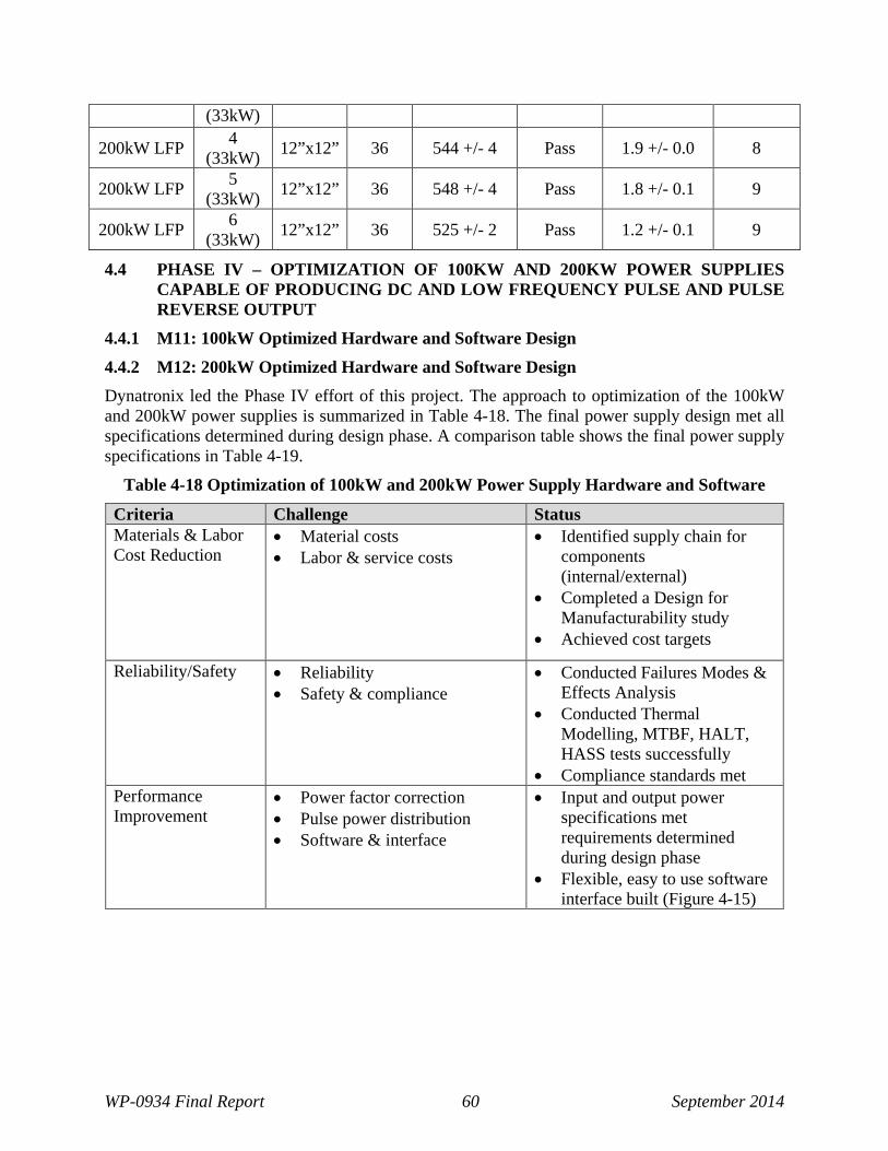
WP-0934 Final Report 60 September 2014
(33kW)
200kW LFP 4 (33kW) 12”x12” 36 544 +/- 4 Pass 1.9 +/- 0.0 8
200kW LFP 5 (33kW) 12”x12” 36 548 +/- 4 Pass 1.8 +/- 0.1 9
200kW LFP 6 (33kW) 12”x12” 36 525 +/- 2 Pass 1.2 +/- 0.1 9
4.4 PHASE IV – OPTIMIZATION OF 100KW AND 200KW POWER SUPPLIES CAPABLE OF PRODUCING DC AND LOW FREQUENCY PULSE AND PULSE REVERSE OUTPUT
4.4.1 M11: 100kW Optimized Hardware and Software Design 4.4.2 M12: 200kW Optimized Hardware and Software Design Dynatronix led the Phase IV effort of this project. The approach to optimization of the 100kW and 200kW power supplies is summarized in Table 4-18. The final power supply design met all specifications determined during design phase. A comparison table shows the final power supply specifications in Table 4-19.
Table 4-18 Optimization of 100kW and 200kW Power Supply Hardware and Software
Criteria Challenge Status Materials & Labor Cost Reduction
• Material costs • Labor & service costs
• Identified supply chain for components (internal/external)
• Completed a Design for Manufacturability study
• Achieved cost targets
Reliability/Safety • Reliability • Safety & compliance
• Conducted Failures Modes & Effects Analysis
• Conducted Thermal Modelling, MTBF, HALT, HASS tests successfully
• Compliance standards met Performance Improvement
• Power factor correction • Pulse power distribution • Software & interface
• Input and output power specifications met requirements determined during design phase
• Flexible, easy to use software interface built (Figure 4-15)

WP-0934 Final Report 61 September 2014
Figure 4-15 Image of control panel for LFP power supply which enables programmability of advanced pulsing waveforms (left) and of oscilloscope output verifying waveform output
(right) Table 4-19: Power supply design comparison
Conventional DC Power
Supply
Existing HFP Power Supply
Existing LFP Power
Supply
LFP Power Supply
(Proposed)
LFP Power Supply
(Designed)
Performance Specifications
Cost (for 100kw) $45,000 $150,000 $150,000 $60,000 ~$60,000
Max Power 500kW < 10kW 200kW 200kW 200kW
Frequency Range
DC DC – 5000Hz DC – 200Hz DC – 200Hz DC – 250Hz
Pulse Reverse N/A Yes Yes Yes Yes
Programmability N/A Full control of programmability
Limited Full control of programmability
Full control of programmability
(Tailored with program
applicable to Integran’s material
processes)
Pulse Parameters
Ripple N/A <1% <5% <1% <1%
Rise Time N/A <50us <1500us <10us <10us
Overshoot N/A negligible Large negligible negligible
Load effect on N/A Minimal Proportional Minimal Minimal

WP-0934 Final Report 62 September 2014
ripple, rise-time, overshoot
distortion at full power
to power output -
Overshoot particularly bad at full
power
distortion at full power
distortion at full power
Footprint Benchmark Much larger than DC
Larger than DC
Comparable to DC – Using
FPGA technology
Comparable to DC – Using
FPGA technology
Modularity N/A N/A
100kW - Single
Module – Limits lower power (10% generally)
100kW = 3x33kW – increased
flexibility of operation
100kW = 3x33kW – increased
flexibility of operation
4.4.3 M13: Optimization of Nanostructured Alloy Plating Process A number of nanostructured alloys systems were investigated in SERDP WP-2173 as potential alternatives to CuBe alloys. The two alloy systems that have shown particular promise for select CuBe applications are (i) Nanostructured Nickel-Cobalt, for applications requiring foil-like materials, and (ii) Nanostructured Cobalt, for bushing type applications that require high strength and galling resistance. These two alloys were selected for scale-up and optimization as part of this project to demonstrate the functionality of the power supplies being developed. The first part of the optimization task was to scale-up the processes to a larger scale that can handle components/parts with higher surface area to demonstrate the higher capacity power supplies, while targeting a component geometry of interest for the particular alloy system. The scale-up of the NiCo alloy system is described below, while the Nano Co-alloy that was optimized for the bushing application is a slight modification to the nCoP system and can use the same tank as described in the previous section with a slightly modified operating window.
Nanostructured NiCo alloy For the Nanostructured NiCo alloy, a 1000L tank, measuring 6’x2’x3’ was designed and constructed which is capable of producing four (4) large nanostructured NiCo foils in one batch. Freestanding foils, measuring 22”x24” in size up to a maximum thickness of 0.012”, can be produced in the tank by electroforming onto a flat stainless steel mandrel and subsequently removing them after plating. The objective of the optimization in this task was to define the operating window as well as the bath replenishment and maintenance schedule to produce multiple batches of foils with low stress, good thickness uniformity and hardness greater than 500VHN. A photograph of the scaled-up tank is shown in Figure 4-16.

WP-0934 Final Report 63 September 2014
Figure 4-16 Images of the scale-up NiCo tank and the mandrel used for electroforming
Using Integran’s high frequency pulse (HFP) plating power supply to provide the benchmark, multiple foils were produced in the scaled-up tank in order to run up the Amp-hrs/L in the tank to determine replenishment chemicals required to maintain a consistent process during heavy use. The quality of each foil was assessed after each run based on appearance, foil composition, hardness and grain size as determined from X-ray diffraction. Once the operating window, replenishment and maintenance schedules were firmly established, a series of electroformed foils were characterized to serve as the baseline property data for future comparison against electroformed foils produced with the 100 and 200kW power supplies. Table 4-20 shows the average composition, hardness and grain size for a series of 10 foils that were produced with the HFP power supply.
Table 4-20 Baseline property data for Nanostructured NiCo alloys produced with an HFP power supply (average of 10 foils)
Property Average Value Std. Dev. (range)
Composition 28 wt% Co ± 4 wt%Co (20-34 wt%Co)
Vickers Hardness 501 VHN ± 12 VHN (475-518 VHN)
Grain size 20 nm ± 1 nm (18 – 22 nm)
4.4.4 M14: 100kW Optimized Power Supply Construction Dynatronix delivered the 100kW LFP power supply to Integran for evaluation. An image of the 100kW power supply is presented in Figure 4-17.

WP-0934 Final Report 64 September 2014
Figure 4-17: Image of 100kW LFP power supply; up to 3 independent channels
4.4.5 M15: 200kW Optimized Power Supply Construction Dynatronix delivered the 200kW LFP power supply to Integran for evaluation. An image of the 200kW power supply is presented in Figure 4-18.
Figure 4-18: Image of 200kW LFP power supply; up to 6 independent channels
4.5 PHASE V – VERIFICATION THAT NANOTECHNOLOGY BASED ELECTROPLATING PROCESS TO REPLACE EHC/CU-BE PROCESSES ARE COMPATIBLE WITH NEW PULSE PLATED POWER SUPPLIES

WP-0934 Final Report 65 September 2014
4.5.1 M16: Verification of nCoP Plating Process with 100kW Unit The results of the demonstration of the optimized 100kW LFP power supply to produce nCoP are detailed in Table 4-21. Coupon size was varied in order to produce deposits at low and optimal % of max output. The appearance of all deposits produced using the power supply appeared bright, shiny and uniform, with no evidence of pits, nodules or other plating defects. There are no significant differences in the adhesion, composition and microstructure of nCoP deposits when produced LFP power supplies.
Table 4-21 Summary of material properties for nCoP deposits produced using the 100kW LFP power supply
Power Supply Channel Coupon
size
% of max
output
Hardness (HV100)
Adhesion Composition (wt%P)
Grain size (nm)
100kW LFP 1 (33kW) 4”x4” 4 522 +/- 6 Pass 1.4 +/- 0.1 9
100kW LFP 1 (33kW) 12”x12” 36 542 +/- 5 Pass 1.5 +/- 0.0 8
100kW LFP 2 (33kW) 12”x12” 36 545 +/- 8 Pass 1.7 +/- 0.1 8
100kW LFP 3 (33kW) 12”x12” 36 523 +/- 2 Pass 1.4 +/- 0.0 8
The 100kW power supply was used in order to produce nCoP coatings to validate reproducibility over a 4 month period. The data shows that the process is operating in accordance with the Technical Data Sheet (see Table 4-22). Namely the microhardness, composition and grain size are all within the acceptable ranges specified.
Table 4-22 nCoP plating process monitoring over 4 mth period to verify reproducibility.

WP-0934 Final Report 66 September 2014
4.5.2 M17: Verification of Nanostructured Alloy Plating Process with 100kW Unit The 100kW LFP power supply consists of three 33kW channels, each capable of providing a maximum current of 1667 Amps each. The unit was demonstrated in the scaled-up Nano NiCo tank by fabricating a series of over 100 foils by using each of three channels in an individual cell in the tank. The composition, hardness and grain size was measured on a sample of ten of the foils produced and compared against the values previously obtained using the HFP power supply. The data shown in Table 4-23 shows that the average properties of the foils produce with the LFP match very closely with those of the foils produced with the standard HFP power supply.
Table 4-23 Property data for Nanostructured NiCo alloys produced with the 100kW LFP compared against those produced with the HFP power supply (average of 10 foils).
Property 100kW LFP Power Supply HFP Power Supply Average Value (stdev)
Range (min – max)
Average Value (stdev)
Range (min – max)
Composition (wt%Co) 29 (±3) 24-32 wt%Co 28 (± 4) 20-34 wt%Co Hardness (VHN) 503 (±7) 491-513 VHN 501 (± 12) 475-518 VHN Grain size (nm) 20 (±2) 16-22 nm 20 (± 1 nm) 18 – 22 nm
4.5.3 M18: Verification of nCoP Plating Process with 200kW Unit The results of the demonstration of the optimized 200kW LFP power supply to produce nCoP are detailed in Table 4-24. Coupon size was varied in order to produce deposits at low and optimal % of max output. The appearance of all deposits produced using the power supply appeared bright, shiny and uniform, with no evidence of pits, nodules or other plating defects. There are no significant differences in the adhesion, composition and microstructure of nCoP deposits when produced LFP power supplies.
Table 4-24 Summary of material properties for nCoP deposits produced using the 200kW LFP power supply
Power Supply Channel Coupon
size
% of max
output
Hardness (HV100)
Adhesion Composition (wt%P)
Grain size (nm)
200kW LFP 1 (33kW) 4”x4” 4 542 +/- 2 Pass 1.6 +/- 0.0 9
200kW LFP 1 (33kW) 12”x12” 36 531 +/- 8 Pass 1.7 +/- 0.1 9
200kW LFP 2 (33kW) 12”x12” 36 534 +/- 4 Pass 1.5 +/- 0.1 8
200kW LFP 3 (33kW) 12”x12” 36 552 +/- 8 Pass 1.8 +/- 0.1 9
200kW LFP 4 (33kW) 12”x12” 36 554 +/- 4 Pass 1.9 +/- 0.0 8
200kW LFP 5 (33kW) 12”x12” 36 538 +/- 4 Pass 1.6 +/- 0.1 9
200kW LFP 6 (33kW) 12”x12” 36 525 +/- 2 Pass 1.2 +/- 0.1 9

WP-0934 Final Report 67 September 2014
The 200kW power supply was also used in order to produce nCoP coating on a conversion roller component sized at 36” length and 4” diameter. The component size is representative of a large landing gear actuator. The output current required for coating represented 45% of max output. The coated part possessed an appearance that was bright, shiny and uniform, with no evidence of pits, nodules or other plating defects as seen in Figure 4-19.
Figure 4-19: Image of nCoP coated conversion roller coated using an optimized 200kW
LFP power supply 4.5.4 M19: Verification of Nanostructured Alloy Plating Process with 200kW Unit The 200kW LFP power supply consists of six 33kW channels, each capable of providing a maximum current of 1667 Amps each (similar to the 100kW unit). In a similar fashion to the 100kW unit, the 200kW power supply was demonstrated by fabricating a series of >100 Nano NiCo foils by using one of the channels in each individual cell in the tank (the tank only has four cells, so only 4 of the six channels we used). The composition, hardness and grain size was measured on a sample of ten of the foils produced and compared against the values previously obtained using the HFP power supply. The data was in Table 4-25 shows that the average properties of the foils produce with the 200kW LFP match very closely with those of the foils produced with both the 100kW LFP as well as the standard HFP power supply. All in all, the data produced for both the 100kW and 200kW LFP power supplies, demonstrate that the power supplies and the nanostructured NiCo process are stable and when used together can produce a material with very consistent material properties.

WP-0934 Final Report 68 September 2014
Table 4-25 Property data for Nanostructured NiCo alloys produced with the 100kW LFP compared against those produced with the HFP power supply (average of 10 foils).
Property
200kW LFP Power Supply HFP Power Supply Average Value (stdev)
Range (min – max)
Average Value (stdev)
Range (min – max)
Composition (wt%Co) 31 (±2) 29-34 wt%Co 28 (± 4) 20-34 wt%Co Hardness (VHN) 504 (±8) 489-517 VHN 501 (± 12) 475-518 VHN Grain size (nm) 19 (±3) 13-23 nm 20 (± 1 nm) 18-22 nm
Large Scale Bushing Demonstration A large diameter nanostructured cobalt alloy bushing was fabricated using the 200kW power supply to serve as an additional demonstration piece. The bushing was fabricated by electroforming a 2mm thick shell of Nanostructured Cobalt-ally onto a steel mandrel measuring 178 mm in diameter and 610mm in length; providing a total surface area of over 3400cm2. Figure 4-20a shows a picture of the part after plating. Following plating, the ends of the bushing where sectioned and the microhardness was measured across the cross-section as shown in Figure 4-20b. Figure 4-21 shows a chart that plot the hardness values as a function of distance across the cross-section which demonstrates that the coating properties are very uniform across the entire cross-section and that the power supply was very stable for the entire duration of plating which lasted over 24 hrs.
(a)
(b)
Figure 4-20 (a) Photograph of large scale electroformed nanostructured cobalt-alloy bushing, and (b) a micrograph of the hardness indents from measurements made across the cross-section.

WP-0934 Final Report 69 September 2014
Figure 4-21 Vickers Microhardnes measurements as a function of the distance across the
cross-section of the large scale electroformed Nanostructured cobalt-alloy bushing. In addition to nNiCo and the nCo-alloys, Integran has developed several advanced alloy systems which may be used to produce multilayered structures using programmable pulse waveforms. The 200kW LFP pulse power supply was used to produce alternating layers of nanocrystalline (NC) and ultra-fine grained (UFG) microstrucutres using the Fe-Ni alloy system. The nanocrystalline deposits are defined by an average grain size of <100 nm while ultra-fine grained deposits are defined by an average grain size of 100-1000 nm. By identifying pulsing conditions for monolithic (i.e., single layer) of both unique microstructures, using programmability a hybrid waveform is developed to alternate microstructures as the material grows. Optical microscopy reveals that this method is successful in producing multilayered structures on length scales of 1-100µm (see Figure 4-22). Additionally, high magnification electron microscopy reveals that this method can extended to length scales of 40-1000nm (see Figure 4-23).
Figure 4-22 Optical micrograph of a multilayered FeNi sample with 5µm NC and 5µm
UFG layers. The NC FeNi layers are shown by the darker shade.

WP-0934 Final Report 70 September 2014
Figure 4-23 Multilayered FeNi sample with 40nm NC layer and 80nm UFG Layer; STEM micrograph (left) and TEM micrograph (right) showing the layer by layer growth of the
multilayered material with well controlled layer thickness and grain size.
5.0 CONCLUSIONS Key achievements made during this program include: (1) design, construction and validation of a 36kW demonstration power supply, (2) design and development of the test protocol and specifications for a 100kW power supply, (3) completion of the 100kW hardware design, (4) completion of the 100kW software design for DC and forward pulse, and (5) identification of candidate demonstration components, scaling of the nCoP plating and activation line to accommodate the large demonstration components and optimization of the Nanostructured alloy system for use as a Cu-Be alternative (6) completion of design, construction and validation of 100 kW power supply, (7) completion of the design and construction of 200 kW power supply, (8) validation of the 100 and 200 kW power supply on components in the nCoP plating and activation line and other alloy systems for Cu-Be alternatives.
The successful completion of this program led to the development of a low-cost, high power output pulse plating power supply that is compatible with Integran’s Nanostructured alloy electroplating processes for use as Hard Chrome and CuBe alternatives. The power supply design is a direct replacement for traditional silicon controlled rectifiers (SCR). The switch mode design leads to improved current regulation and reduced package size/footprint. The high power output systems consist of multiple modules mounted on a single base for ease of transportation and installation. Each module may be operated independently or in conjunction to achieve current outputs ranging from 100A up to 10,000A at 20V. Programmable controls are available including current, voltage or cross-over regulation modes. The range of current outputs available enables use of the power supplies for coating of components at DoD maintenance depot across the range of part size encountered.
A cost reduction of 3X-4X was achieved using the LFP pulse power supplies relative to traditional high frequency pulse power supplies. (i.e., achieves cost target of $100,000/100kW).

WP-0934 Final Report 71 September 2014
6.0 APPENDICES APPENDIX A: POINTS OF CONTACT
POINT OF CONTACT Name
ORGANIZATION Name
Address
Phone Fax
Role in Project
Neil Mahalanobis Integran Technologies, Inc 6300 Northam Drive
Mississauga, ON L4V 1H7
416-675-6266 x 375 416-675-1666
Principal Investigator
Dennis J. Malecek Dynatronix Inc. 462 Griffin Blvd. Amery WI 54001
(715) 268-8118 (715) 268-8183
Subcontractor

WP-0934 Final Report 72 September 2014
APPENDIX B: 100KW & 200KW POWER SUPPLY SPECIFICATIONS

WP-0934 Final Report 73 September 2014

WP-0934 Final Report 74 September 2014

WP-0934 Final Report 75 September 2014
APPENDIX C: 100KW POWER SUPPLY SPECIFICATIONS REQUIREMENTS
Requirement Value(s) Conditions/description 1. Outputs and ratings
1.1. Voltage 0 – 20 volts 0.1V resolution
Peak or average output voltage range. Pulse and DC operation.
1.2. Peak Current 0 – 5000 amps, 1A resolution Peak output current range of power supply.
1.3. Average current 0 – 5000 amps Average output current. 1.4. Operating range 0 – 5000 amps
(current mode control) 0 – 20.00 volts (voltage mode control)
-
1.4.1. Recommended Operating Range
100 – 5000A Current control 1 – 20V Voltage control
Range over which dynamic specifications (pulse) will be met.
1.5. Maximum Output Power 100kW Available output power. 1.6. Multiple Outputs Up to 3 The power supply can be configured to have multiple,
independently regulated outputs that can be connected in parallel to deliver the full rated current from the system or independently
1.7. Timing requirements (pulse mode)
The output can be set to pulse using a set of six timing parameters.
1.7.1. FDIR 0-999msec Time duration that the output has positive polarity. Current flowing out through the “+” or anode terminal and back through the “-” or cathode terminal.
1.7.1.1. FCYCLE FTON + FTOFF The period of the pulse waveform in the forward direction 1.7.1.2. FTON 4-999msec Time per FCYCLE that output is active(on) 1.7.1.3. FTOFF 0-999msec Time per FCYCLE that the output is inactive(off)
1.7.2. RDIR 0-999msec Time duration that the output has NEGATIVE polarity. Current flowing out through the “-” or cathode terminal and back through the “+” or anode terminal.

WP-0934 Final Report 76 September 2014
Requirement Value(s) Conditions/description 1.7.2.1. RCYCLE RTON + RTOFF The period of the pulse waveform in the reverse direction 1.7.2.2. RTON 4-999msec Time per RCYCLE that output is active(on) 1.7.2.3. RTOFF 0-999msec Time per RCYCLE that the output is inactive(off)
1.8. Output regulation 1.8.1. Voltage regulation
(line or load) Greater of ± 1% of setting or 0.1% of max. rating.
Measured at power supply output terminals.
1.8.2. Current regulation (line or load)
Greater of ± 1% of setting or 0.1% of max. rating.
Measured using series metering shunt and a voltage meter of sufficient precision.
1.9. Output overshoot 1.9.1.Voltage Overshoot ≤ 50% of peak amplitude or
≤5% of peak output rating. Measured at the output terminals of the power supply during steady state pulsing conditions.
1.9.2. Current overshoot ≤ 10% of peak amplitude setting or
≤1% of peak output rating.
Measured using TBD during steady state pulsing conditions.
1.10. Output Rise Time 1.10.1. Voltage Rise Time ≤ 1msec Under same conditions as 1.9.1. Measured from 10% to
90% of peak output at power supply output terminals. 1.10.2. Current Rise Time ≤ 3msec Under same conditions as 1.9.2. Measured from 10% to
90% of peak output.
1.11. Output Fall Time 1.11.1. Voltage Fall Time ≤ 1msec Under same conditions as 1.9.1. Measured from 10% to
90% of peak output at power supply output terminals. 1.11.2. Current Fall Time ≤ 3msec Under same conditions as 1.9.2. Measured from 10% to
90% of peak output. 1.12. Safe Operating Load
range 0 ohms to Infinity Power supply will not be damaged when applied to load
range shown. 1.13. Typical Operating 0.4mohm to 100.0 mohms -

WP-0934 Final Report 77 September 2014
Requirement Value(s) Conditions/description Load range.
1.14. Output ripple <1% RMS of maximum rated output voltage
Minimize as long as not a significant cost penalty
1.15. RMS Noise, Hum, Ripple, Droop
<1% RMS of maximum rated output voltage
Under same conditions as 1.8.1
1.16. Options None 2. Physical Connections
2.1. Output Connections Bus bar Output wiring to load must consist of multiple twisted pair, laminated busbars or equivalent low inductance connection.
2.2. Power Connections Terminal block Customer is responsible for ensuring power supply is connected to power source in accordance with local, national and international standards/codes.
3. Metering & Controls 3.1.1.Voltage regulation
(line or load) Greater of ± 1% of setting or 0.1% of max. rating +LSD
Measured at power supply output terminals.
3.1.2. Current regulation (line or load)
Greater of ± 1% of setting or 0.1% of max. rating +LSD
Measured using series metering shunt and a voltage meter of sufficient precision.
3.2. Output Charge All charge metering is updated every 100msec in this particular system. Metering range is selectable using a software utility provided with the power supply.
3.2.1.Ampere•Time Totalizer 9999.999, 99999.99, 999999.9 or 9999999 A•min or A•hours
Resolution is dependent on the sum of the peak output currents for all channels and the update rate listed above.
3.2.2.Ampere•Time Control (ATC)
9.999, 99.99, 999.9, 9999A•min or A•hours
Accumulates charge using the same method and same resolution as the Ampere•Time Totalizer. Resolution is dependent on the sum of the peak output currents for all channels and the update rate listed above.
4. Input Power 480VAC, Three Phase, 50-60Hz,

WP-0934 Final Report 78 September 2014
Requirement Value(s) Conditions/description 150 Amps
5. Mechanical Specifications 5.1. Overall Size No greater than
6’W x 6’H x 6’D System will follow a modular construction scheme. Applications may require multiple outputs programmed to different current or voltage amplitudes with common pulse timing requirements. Three to four modules/channels should be sufficient for most applications. These can be wired in parallel to achieve the full rated output or can be wired independently to achieve better current distribution/density on the part being plated.
5.2. Weight < 5000lbs. Enable transportation by forklift 5.3. Cooling Air or liquid Air cooling preferred
6. Hardware & Firmware Architecture
6.1. Control Options 6.1.1. Local/manual or
simple An optional local control module that allows user to make basic settings with a relatively rudimentary interface. Controls limited to two rotary encoders and two momentary push buttons. Menu system will be available to access advanced features through this controller while consulting the user manual.
6.1.2. Local/Touch Screen or advanced
This controller replaces the Simple control interface and enables user friendly menus to ease programming and setup of the power supply though the local interface.
6.1.3. Remote Host Connection
Windows-based program for setting, monitoring, controlling power supply system
7. Environmental 7.1. Operating 0-40°C , 20-75% humidity (non
condensing) -
7.2. Storage -20-85C ,20-75% humidity(non condensing)
-
8. Standards & Compliance

WP-0934 Final Report 79 September 2014
Requirement Value(s) Conditions/description 8.1. ETL Listing Required -
8.2. CE Marking Required - 8.2.1. EMC Required - 8.2.2. Safety Required -

WP-0934 Final Report 80 September 2014
Appendix D: WEAR ANALYSIS IMAGES
Figure 6-1 - Sample ID: nCoP-1 Wt.% P (AD); SE micrographs of sliding wear track.

WP-0934 Final Report 81 September 2014
Figure 6-2 - Wear Pin [nCoP-1 Wt.% P (AD)] ; SE micrographs of the wear scar on the
wear pin.
Transferred nCoP

WP-0934 Final Report 82 September 2014
Figure 6-3 – Sample ID: nCoP-1 Wt.% P (HT); SE micrographs of sliding wear track.

WP-0934 Final Report 83 September 2014
Figure 6-4 - Wear Pin [nCoP-1 Wt.% P (HT)]; SE micrographs of the wear scar on the
wear pin.
Transferred nCoP

WP-0934 Final Report 84 September 2014
Figure 6-5 – Sample ID: nCoP-2 Wt.% P (AD); SE micrographs of sliding wear track.

WP-0934 Final Report 85 September 2014
Figure 6-6 - Wear Pin [nCoP-2 Wt.% P (AD)]; SE micrographs of the wear scar on the
wear pin.
Transferred nCoP

WP-0934 Final Report 86 September 2014
Figure 6-7 – Sample ID: nCoP-2 Wt.% P (HT); SE micrographs of sliding wear track.

WP-0934 Final Report 87 September 2014
Figure 6-8 - Wear Pin [nCoP-2 Wt.% P (HT)]; SE micrographs of the wear scar on the
wear pin.
Transferred nCoP

WP-0934 Final Report 88 September 2014
Appendix E: TEM MICROSCOPY IMAGES
Figure 6-9 – Sample ID: nCoP-1 Wt.% P (AD) #1; TEM bright field, dark field and selected area
diffraction (SAD) microscopy images. Magnification indicated below each image.

WP-0934 Final Report 89 September 2014
Figure 6-10 – Sample ID: nCoP-1 Wt.% P (AD) #2; TEM bright field and dark field microscopy
images. Magnification indicated below each image.

WP-0934 Final Report 90 September 2014
Figure 6-11 – Sample ID: nCoP-1 Wt.% P (HT) #1; TEM bright field and dark field microscopy
images. Magnification indicated below each image.

WP-0934 Final Report 91 September 2014
Figure 6-12 – Sample ID: nCoP-1 Wt.% P (HT) #2; TEM bright field and dark field microscopy
images. Magnification indicated below each image.

WP-0934 Final Report 92 September 2014
Figure 6-13 – Sample ID: nCoP-2 Wt.% P (AD) #1; TEM bright field, dark field and selected
area diffraction (SAD) microscopy images. Magnification indicated below each image.

WP-0934 Final Report 93 September 2014
Figure 6-14 – Sample ID: nCoP-2 Wt.% P (AD) #2; TEM bright field and dark field microscopy
images. Magnification indicated below each image.

WP-0934 Final Report 94 September 2014
Figure 6-15 – Sample ID: nCoP-2 Wt.% P (HT) #1; TEM bright field and dark field microscopy
images. Magnification indicated below each image.

WP-0934 Final Report 95 September 2014
Figure 6-16 – Sample ID: nCoP-2 Wt.% P (HT) #2; TEM bright field, dark field and selected
area diffraction (SAD) microscopy images. Magnification indicated below each image.

WP-0934 Final Report 96 September 2014
7.0 REFERENCES 1 DOD-STD-2182 (January 29, 1985) 2 MIL-P-19419A (August 21, 1989), now used only for replacement purposes. 3 D.T. Gawne et al. J.Vac. Sci. Tech., A3 (6), 2334 (1985); Tribology International, 17, 123 (1992). 4 UK Chromium Plating Regulations 1931 (amended in 1973), HMSO (1073). 5 OSHA, Occupational Exposure to Hexavalent Chromium, (2006) 6 “Minimizing the Use of Hexavalent Chromium (Cr6+),” United States of America, Department of Defense, The Under Secretary of Defense, April 8, 2009 7 United States Environmental Protection Agency. Hazard Summary – Created in April 1992; Revised in January 2000. Available at http://www.epa.gov/ttn/atw/hlthef/berylliu.html 8 U. Erb and A. M. El-Sherik, US Patent No. 5,352,266, 1994 9 U. Erb, A.M. El-Sherik, C. Cheung, M.J. Aus, US Patent No. 5,433,797, 1995 10 G. Palumbo, I. Brooks, J. McCrea, G.D. Hibbard, F. Gonzalez, K. Tomantschger and U. Erb. US Patent Application 20050205425, September 22, 2005. 11 D. Facchini, J.L. McCrea, F. Gonzalez, K. Tomantschger and G. Palumbo, Product Finishing, April, 2009, 14 12 B. D. Sartwell, P. M. Natishan, K. O. Legg, J.D. Schell and J. P. Sauer, AESF Plating Forum, March 1998 13 D. Facchini, F. Gonzalez. J. McCrea, M. Uetz, G. Palumbo, K, Tomantschger, N. Nagarajan, J. Victor, U. Erb, US Patent No. 8,545,994, 2013 14 G. McMahon and U. Erb, Microstructural Science, vol. 17, p. 447 (1989) 15 G. McMahon and U. Erb, Journal of Materials Science Letters, vol. 8, p. 865 (1989) 16 R.T.C. Choo, A. M. El-Sherik, J. Toguri and U. Erb, J. Appl. Electrochem., 25, 1995, 384 17 G Palumbo, F. Gonzalez, et al., US Patent No. 5,527,445 18 da Silva, M., C. Wille, U. Klement, P. Choi, & T. Al-Kassan, Materials Science and Engineering, A 445-446 (2007) 31-39