
Final Front Pages
16
i CERTIFICATE This is to certify that this Dissertation entitled “Design of Frequency Reconfigurable Microstrip Patch Antenna” has been successfully carried out by Ghanshyam Singh (Enrolment No.: 09E2UCDCM30P601) , under my supervision and guidance, in partial fulfillment of the requirement for the award of Master of Technology Degree in Digital Communication from University College of Engineering, Rajasthan Technical University, Kota for the Year 2009-2011. Supervisor Dr. Mithilesh Kumar (Associate Professor) Dept. of Electronics Engineering, Rajasthan Technical University, Kota
-
Upload
mukesh-kumar-baliwal -
Category
Documents
-
view
214 -
download
0
Transcript of Final Front Pages

7/27/2019 Final Front Pages
http://slidepdf.com/reader/full/final-front-pages 1/16

7/27/2019 Final Front Pages
http://slidepdf.com/reader/full/final-front-pages 2/16
ii
ACKNOWLEDGEMENTS
It would be a great pleasure to write a few words, which would although not suffice as the
acknowledgement of this long cherished effort, but in the absence of which this work would
necessarily be incomplete. So these words of acknowledgement come as a small gesture of
gratitude towards all those people, without whom the successful completion of this project would
not have been possible.
Firstly I owe my profound gratitude to my supervisor Dr. Mithilesh Kumar (Asso. Prof.) for
their valuable guidance, supervision, constant support and encouragement which have made me
as a constant oasis of ideas and passion in science which exceptionally inspire and enrich my
knowledge to complete this dissertation work.
I would like to express deep gratitude towards Dr. Rajeev Gupta (Prof. and Head, Electronics
Engineering Deptt. UCE, Kota). He is like a beam of light for us. His kind guidance showed us
the path of life and is unforgettable.
Also special Thanks and due regards extends to Dr. R. S. Meena, Mr. Pankaj Shukla (Asso.
Prof.), Dr. Girish Parmar and Mr. Deepak Bhatia (Asst. Prof. at UCE, RTU, Kota) for they
extended towards their valuable guidance, indispensable help and inspiration at times. In
appreciation I offer them my sincere gratitude.
I would like to convey my special thanks to Mr. S. P. Chakraborty, C.A.R.E. IIT Delhi for his
untiring technical support. Without his positive attitude and moral support, the project would
have not been completed in time.
Last but not least we would like to thank the Department of Electronics Engineering, UCE Kota
for providing us with the facilities at lab, my beloved family and all my friends and the almighty
god for his blessings. It would have been impossible for me to complete the work without their
valuable guidance & prompt cooperation.
Date Ghanshyam Singh

7/27/2019 Final Front Pages
http://slidepdf.com/reader/full/final-front-pages 3/16
iii
ABSTRACT
Planar antennas are extensively used in various wireless and mobile applications. The continuous
growth and commercial interest in wireless communications, especially in personal and mobile
communication systems significantly increases the demand for low cost, compact size, multiple
bands and high performance antennas, which are the key components, used in any
communication systems. The reduction of the antenna’s size, the multiplicity of bands, the ease
of designing the antenna (simple structure) and the need for flexible specifications such as
independent control, is very important in the design of new antennas.
Reconfigurable antennas have more advantages in terms of increasing the antenna capabilities by
tuning or switching its performances. Therefore, the needs to design compact size, simple
structure, low profile, multiple bands antennas are required.
The ability of reconfigurable antennas to tune resonances, change polarization and modify their
radiation patterns, made their development imperative in modern telecommunication systems.
Their agility and diversity created new horizons for different types of applications especially in
cognitive radio, multiple input multiple output systems, satellites and many other applications.
Reconfigurable antennas satisfy the requirements for increased functionality, such as direction
finding, beam steering, radar, control and command, within a confined volume.
Since their rise in the last decade, reconfigurable antennas have made use of many
reconfiguration techniques. The most common techniques utilized revolved around switching
mechanisms. By combining low-loss, high-isolation switches such as MEMS or PIN diode
switches with compatible antenna elements, we can physically reconfigure antennas and their
feed structures providing frequency and polarization diversity. Other techniques such as the
incorporation of variable capacitors, varactors and physical structure alteration surfaced recently
to overcome many problems faced in using switches and their biasing.
Firstly in this work basic conventional microstrip rectangular and circular antenna structures are
designed with the help of standard designing procedures.

7/27/2019 Final Front Pages
http://slidepdf.com/reader/full/final-front-pages 4/16
iv
After the conventional structure designing, a novel frequency reconfigurable antenna design and
development is proposed for wireless devices. In the first proposed design, a rectangular patch
antenna with square slot using two PIN diodes at the centre frequency 10 GHz was designed and
simulated frequency reconfiguration is achieved in the frequency range of 10-10.5 GHz and the
measured results shows the same effect in the frequency range of 10.216-10.552 GHz. The
frequency reconfiguration is carried out by switching the diodes on/off states.
After that this same technique is used for the frequency reconfiguration of the circular patch
antenna. In the second proposed design, a circular patch antenna with circular slot using two PIN
diodes at the centre frequency 10 GHz was designed and simulated frequency reconfiguration is
achieved in the frequency range of 9.69-10.2 GHz and the measured results shows the same
effect in the frequency range of 10.33-11.01 GHz.
In the fabricated structure of proposed geometry the diodes are replaced by microstrip line for
on-state as an ideal case. The antenna is designed on FR4 substrate (= 4.54) of thickness (h)
1.6 mm. The proposed structure was simulated by using the electromagnetic (EM) simulation
software. The optimized structure was fabricated using microwave integrated circuit (MIC)
techniques on same substrate. The return loss was measured using the Vector Network Analyzer.
The simulated and measured return loss shows the close agreement.

7/27/2019 Final Front Pages
http://slidepdf.com/reader/full/final-front-pages 5/16
v
LIST OF FIGURES
Figure No. Figure Name Page No.
1.1 Flow chart of the process involved in this project 7
3.1 Basic wave travelling model of s-parameters. 17
3.2 Basic conventional rectangular microstrip patch Antenna structure 20
3.3 Return loss at 10.1 GHz resonance frequency 20
3.4 Insertion loss at 10.1 GHz resonance frequency 21
3.5 Comparison of return loss and insertion loss 21
3.6 E-Field radiation pattern for conventional rectangular patch 22
3.7 H-Field radiation pattern for conventional rectangular patch 22
3.8 Basic conventional circular microstrip patch Antenna structure 24
3.9 Return loss at 10.058 GHz resonance frequency 24
3.10 Insertion loss at 10.058 GHz resonance frequency 25
3.11 Comparison of return loss and insertion loss 25
3.12 E-Field radiation pattern for conventional circular patch 26
3.13 H-Field radiation pattern for conventional circular patch 26
4.1 When both diodes (D1 & D2) are in OFF-state 30
4.2 Return loss at 10.5 GHz resonance frequency 30
4.3 Insertion loss at 10.5 GHz resonance frequency 31

7/27/2019 Final Front Pages
http://slidepdf.com/reader/full/final-front-pages 6/16
vi
Figure No. Figure Name Page No.
4.4 Comparison of return loss and insertion loss 31
4.5 E-Field radiation pattern when both diodes (D1 & D2) are in OFF-state
32
4.6 H-Field radiation pattern when both diodes (D1 & D2) are in OFF-
state
32
4.7 When one diode (D1) is in ON-state 33
4.8 Return loss at 10.3GHz resonance frequency 34
4.9 Insertion loss at 10.3GHz resonance frequency 34
4.10 Comparison of return loss and insertion loss 35
4.11 E-Field radiation pattern when one diode (D1) is in ON-state 35
4.12 H-Field radiation pattern when one diode (D1) is in ON-state 36
4.13 When both diodes (D1 & D2) are in ON-state 37
4.14 Return loss at 10.2GHz resonance frequency 37
4.15 Insertion loss at 10.2GHz resonance frequency 38
4.16 Comparison of return loss and insertion loss 38
4.17 E-Field radiation pattern when both diodes (D1 & D2) are in ON-state 39
4.18 H-Field radiation pattern when both diodes (D1 & D2) are in ON-state 39
4.19 Fabricated structure when diodes (D1 & D2) are in OFF-state 41
4.20 Measured result when diodes (D1 & D2) are in OFF-state 42

7/27/2019 Final Front Pages
http://slidepdf.com/reader/full/final-front-pages 7/16
vii
Figure No. Figure Name Page No.
4.21 Simulated and measured return loss for case-I 42
4.22 Fabricated structures when one diode (D1) is in ON-state 43
4.23 Measured result when one diode (D1) is in ON-state 43
4.24 Simulated and measured Return loss for case-II 44
4.25 Fabricated structures when diodes (D1 & D2) are in ON-state 44
4.26 Measured result when diodes (D1 & D2) are in ON-state 45
4.27 Simulated and measured return loss for case-III 45
4.28 Comparison of simulated return losses 46
4.29 Comparison of measured return losses 47
5.1 When both diodes (D1 & D2) are in OFF-state 50
5.2 Return loss at 9.69 GHz resonance frequency 50
5.3 Insertion loss at 9.69 GHz resonance frequency 51
5.4 Comparison of return loss and insertion loss 51
5.5 E-Field radiation pattern when both diodes (D1 & D2) are in OFF-
state
52
5.6 H-Field radiation pattern when both diodes (D1 & D2) are in OFF-
state
52
5.7 When one diode (D1) is in ON-state 53
5.8 Return loss at 9.83 GHz resonance frequency 54

7/27/2019 Final Front Pages
http://slidepdf.com/reader/full/final-front-pages 8/16
viii
Figure No. Figure Name Page No.
5.9 Insertion loss at 9.83 GHz resonance frequency 54
5.10 Comparison of return loss and insertion loss 55
5.11 E-Field radiation pattern when one diode (D1) is in ON-state 55
5.12 H-Field radiation pattern when one diode (D1) is in ON-state 56
5.13 When both diodes (D1 & D2) are in ON-state 57
5.14 Return loss at 10.2GHz resonance frequency 57
5.15 Insertion loss at 10.2GHz resonance frequency 58
5.16 Comparison of return loss and insertion loss 58
5.17 E-Field radiation pattern when both diodes (D1 & D2) are in ON-state 59
5.18 H-Field radiation pattern when both diodes (D1 & D2) are in ON-state 59
5.19 Fabricated structure when diodes (D1 & D2) are in OFF-state 60
5.20 Measured result when diodes (D1 & D2) are in OFF-state 61
5.21 Measured and simulated return losses for case-I 61
5.22 Fabricated structures when one diode (D1) is in ON-state 62
5.23 Measured result when one diode (D1) is in ON-state 62
5.24 Measured and simulated return loss for case-II 63
5.25 Fabricated structures when diodes (D1 & D2) are in ON-state 63
5.26 Measured result when diodes (D1 & D2) are in ON-state 64

7/27/2019 Final Front Pages
http://slidepdf.com/reader/full/final-front-pages 9/16
ix
Figure No. Figure Name Page No.
5.27 Measured and simulated return losses for case-III 64
5.28 Comparison of simulated return losses 65
5.29 Comparison of measured return losses 66

7/27/2019 Final Front Pages
http://slidepdf.com/reader/full/final-front-pages 10/16
x
LIST OF SYMBOLS
S. No. Symbols Description
1 - Dielectric Constant of Substrate
2 - Wavelength
3 L - Length of Patch Element
4 W - Width of Patch Element
5 c - Speed of Light
6 h - Height of Dielectric Substrate
7 t - Thickness of Patch Element
8 - Free Space Wavelength
9 - Effective Dielectric Constant
10 - Length Extension of Patch
11 - Characteristic Impedance
12 d - Distance of the Port-excitation from the Patch
13 - Incident Power
14 - Reflected Power
15 - Quarter Wave Line Impedance
16 - Antenna Impedance
7/27/2019 Final Front Pages
http://slidepdf.com/reader/full/final-front-pages 11/16
xi
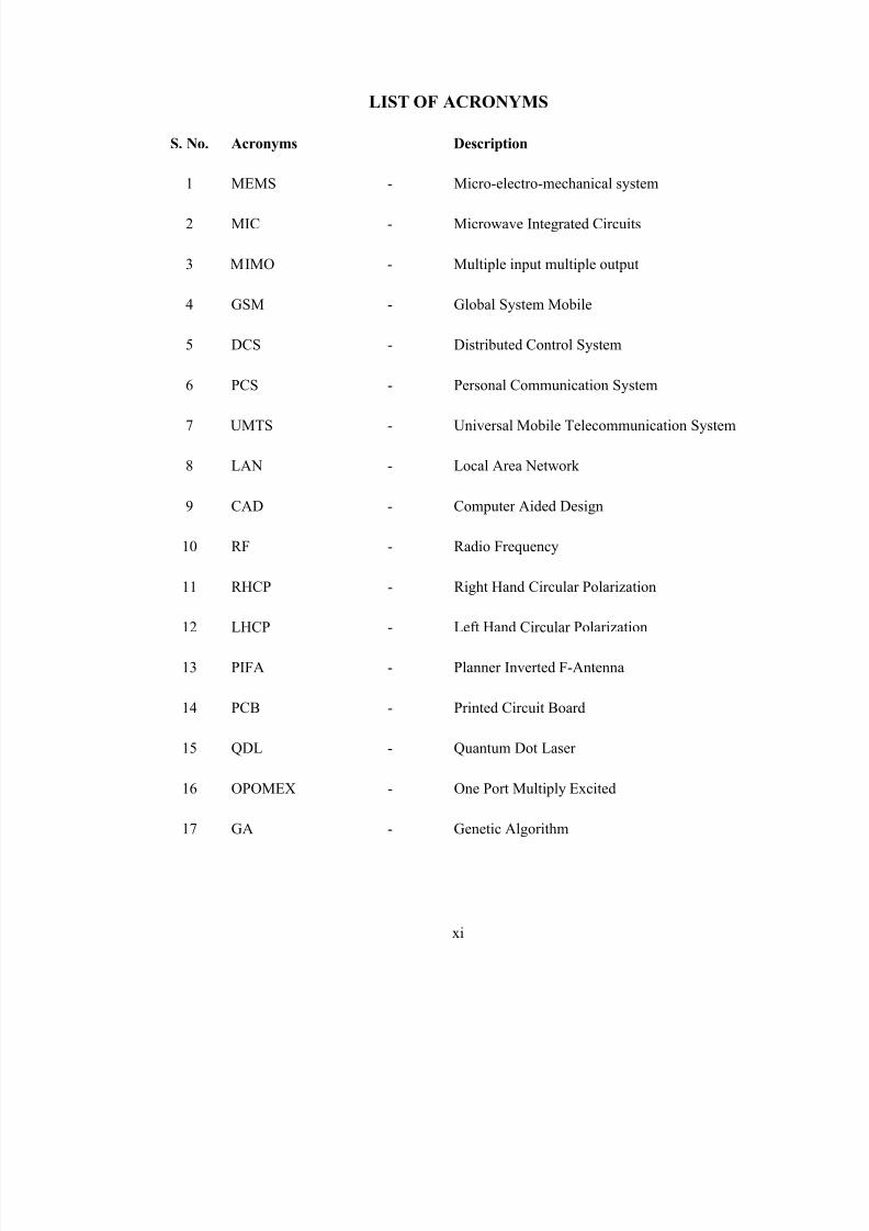
LIST OF ACRONYMS
S. No. Acronyms Description
1 MEMS - Micro-electro-mechanical system
2 MIC - Microwave Integrated Circuits
3 MIMO - Multiple input multiple output
4 GSM - Global System Mobile
5 DCS - Distributed Control System
6 PCS - Personal Communication System
7 UMTS - Universal Mobile Telecommunication System
8 LAN - Local Area Network
9 CAD - Computer Aided Design
10 RF - Radio Frequency
11 RHCP - Right Hand Circular Polarization
12 LHCP - Left Hand Circular Polarization
13 PIFA - Planner Inverted F-Antenna
14 PCB - Printed Circuit Board
15 QDL - Quantum Dot Laser
16 OPOMEX - One Port Multiply Excited
17 GA - Genetic Algorithm

7/27/2019 Final Front Pages
http://slidepdf.com/reader/full/final-front-pages 12/16
xii
S. No.
18
Acronyms
VSWR -
Description
Voltage Standing Wave Ratio
19 HPBW - Half Power Beam Width
20 IEEE - Institute of Electrical & Electronics Engineers
21 TEM - Transverse Electric-Magnetic
22 3D - Three-Dimensional
23 VNA - Vector Network Analyzer
24 RCS - Radar Cross Section

7/27/2019 Final Front Pages
http://slidepdf.com/reader/full/final-front-pages 13/16
xiii
CONTENTS
CERTIFICATE i
ACKNOWLEDGEMENTS ii
ABSTRACT iii
LIST OF FIGURES v
LIST OF SYMBOLS x
LIST OF ACRONYMS xi
CHAPTER 1: INTRODUCTION TO RECONFIGURABLE ANTENNAS 1-8
1.1 Introduction 1
1.2 Reconfigurable Antennas Classifications and Categories 1
1.3 Reconfigurable Antennas Functional Mechanism 2
1.4 Reconfigurable Antennas Applications 3
1.5 Microstrip Patch Antenna 4
1.6 Advantages of Microstrip Patch Antenna 4
1.7 Scope of Work 5
1.8 Problem Statement 5
1.9 Methodology of the Project 6
1.10 Project Implementation Strategy 6
1.11 Dissertation Overview 8
CHAPTER 2: LITERTATURE REVIEW 9-14
2.1 Introduction 9

7/27/2019 Final Front Pages
http://slidepdf.com/reader/full/final-front-pages 14/16
xiv
2.2 Reconfigurable Antennas using Switches 9
2.3 Reconfigurable Antennas using Capacitors or Varactors 11
2.4 Reconfigurable Antennas using Physical Angular Alteration 11
2.5 Reconfigurable Antennas using Different Biasing Networks 12
2.6 Reconfigurable Antenna array 12
2.7 Antennas using Reconfigurable Feeding Networks 12
2.8 Biasing of Switches in Reconfigurable Antenna Structures 13
2.8.1 The Biasing of RF MEMS 13
2.8.2 Biasing of p-i-n and Schottky diodes 14
CHAPTER 3: DESIGN OF CONVENTIONAL MICROSTRIP
PATCH ANTENNA 15-26
3.1 Introduction 15
3.2 Design of Conventional Rectangular Patch Antenna 15
3.2.1 The Design Specifications 15
3.2.2 The S-parameters 17
3.2.3 Radiation Pattern 18
3.2.4 Simulated Structure and Results 19
3.3 Basic Conventional Circular Microstrip Patch Antenna 23
3.3.1 Quarter Wave Transformer 23
3.3.2 Simulated Structure and Results 23

7/27/2019 Final Front Pages
http://slidepdf.com/reader/full/final-front-pages 15/16
xv
CHAPTER 4: FREQUENCY RECONFIGURABLE RACTANGULAR
PATCH ANTENNA DESIGN 27-47
4.1 Introduction 27
4.2 Frequency Reconfigurable Rectangular Patch Antenna Structure 28
4.3 Simulated Structures and Results 29
4.3.1 Case-I When Both Diodes (D1 & D2) are in OFF-State 29
4.3.2 Case-II When One Diode (D1) is in ON-State 33
4.3.3 Case-III When Both Diodes (D1 & D2) are in ON-State 36
4.4 Fabricated Structures and Results 40
4.4.1 Fabrication Procedure for Microstrip Patch Antenna 40
4.4.2 Case-I When Both Diodes (D1and D2) are in OFF-State 41
4.4.3 Case-II When One Diode (D1) is in ON-State 43
4.4.4 Case-III When Both Diodes (D1 & D2) are in ON- State 44
4.5 Comparison of Simulated and Measured Return Losses for three cases 46
CHAPTER 5: FREQUENCY RECONFIGURABLE CIRCULAR
PATCH ANTENNA DESIGN 48-66
5.1 Introduction 48
5.2 Reconfigurable Circular Microstrip Patch Antenna Structure 48
5.3 Simulated Structures and Results for Circular Patch Antenna 49
5.3.1 Case-I When Both Diodes (D1 & D2) are in OFF-State 49
5.3.2 Case-II When One Diode (D1) is in ON-State 53

7/27/2019 Final Front Pages
http://slidepdf.com/reader/full/final-front-pages 16/16
xvi
5.3.3 Case-III When Both Diodes (D1 & D2) are in ON-State 56
5.4 Fabricated Structures and Results of Circular Patch 60
5.4.1 Case-I When Both Diodes (D1 and D2) are in OFF-State 60
5.4.2 Case-II When One Diode (D1) is in ON-State 62
5.4.3 Case-III When Both Diodes (D1 & D2) are in ON- State 63
5.5 Comparison of Simulated and Measured Return Losses for three cases 65
CHAPTER 6: CONCLUSIONS AND FUTURE WORK 67
REFERENCES 69