электронные таблицы основные параметры электронных таблиц основные типы и форматы данных

SIM868_Hardware_Design_V1.03
SIMCOM C
ONFIDENTIA
L FILE

Smart Machine Smart Decision
SIM868_Hardware_Design_V1.03 1 2017-02-18
Document Title SIM868 Hardware Design
Version V1.03
Date 2017-02-18
Status Release
Document Control ID SIM868_Hardware_Design_V1.03
General Notes SIMCom offers this information as a service to its customers, to support application and engineering efforts that use the products designed by SIMCom. The information provided is based upon requirements specifically provided to SIMCom by the customers. SIMCom has not undertaken any independent search for additional relevant information, including any information that may be in the customer’s possession. Furthermore, system validation of this product designed by SIMCom within a larger electronic system remains the responsibility of the customer or the customer’s system integrator. All specifications supplied herein are subject to change. Copyright This document contains proprietary technical information which is the property of SIMCom Limited, copying of this document and giving it to others and the using or communication of the contents thereof, are forbidden without express authority. Offenders are liable to the payment of damages. All rights reserved in the event of grant of a patent or the registration of a utility model or design. All specification supplied herein are subject to change without notice at any time. Copyright © Shanghai SIMCom Wireless Solutions Ltd. 2017
SIMCOM C
ONFIDENTIA
L FILE
Smart Machine Smart Decision
SIM868_Hardware_Design_V1.03 2 2017-02-18
Contents
1. Introduction ........................................................................................................ 10
2. SIM868 Overview .............................................................................................. 10
2.1. SIM868 Key Features ......................................................................................................... 11
2.2. Operating Modes ................................................................................................................. 14
2.3. Functional Diagram............................................................................................................. 15
3. Package Information ......................................................................................... 16
3.1. Pin Out Diagram ................................................................................................................. 16
3.2. Pin Description .................................................................................................................... 17
3.3. Package Dimensions ........................................................................................................... 19
4. Application Modes of SIM868 .......................................................................... 22
4.1. All-in-one Mode .................................................................................................................. 22
4.2. Stand-alone Mode ............................................................................................................... 23
5. Application Interface of GSM .......................................................................... 24
5.1. Power Supply of GSM ........................................................................................................ 24
5.2. Reference Circuit of GSM Power Supply ........................................................................... 25
5.3. Power on/off GSM Part ....................................................................................................... 26 5.3.1. Power on GSM .................................................................................................................................... 26
5.3.2. Power off GSM ................................................................................................................................... 27
5.4. Power Saving Mode of GSM .............................................................................................. 28 5.4.1. Minimum Functionality Mode of GSM Part ....................................................................................... 28
5.5. Serial Port of GSM .............................................................................................................. 29 5.5.1. Function of Serial Port ........................................................................................................................ 30
5.5.2. Serial Interfaces ................................................................................................................................... 30
5.5.3. Debug Interface ................................................................................................................................... 32
5.5.4. Software Upgrade of GSM .................................................................................................................. 33
5.6. UART1_RI Behaviors ......................................................................................................... 33
5.7. Audio Interfaces .................................................................................................................. 34 5.7.1. Speaker Interfaces Configuration ........................................................................................................ 35
5.7.2. Microphone Interfaces Configuration ................................................................................................. 36
5.7.3. Audio Electronic Characteristic .......................................................................................................... 36
5.7.4. TDD Noise of GSM ............................................................................................................................ 36
5.8. SIM Card Interface.............................................................................................................. 37 5.8.1. SIM Card Application ......................................................................................................................... 37
5.8.2. SIM Card Design Guide ...................................................................................................................... 38
5.8.3. Design Considerations for SIM Card Holder ...................................................................................... 39
5.9. SD Interface ........................................................................................................................ 41
5.10. I2C Bus ............................................................................................................................... 41
5.11. ADC .................................................................................................................................... 41
SIMCOM C
ONFIDENTIA
L FILE

Smart Machine Smart Decision
SIM868_Hardware_Design_V1.03 3 2017-02-18
5.12. Network Status Indication ................................................................................................... 42
5.13. Operating Status Indication ................................................................................................. 42
5.14. RF Synchronization Signal ................................................................................................. 43
5.15. Antenna Interface of GSM .................................................................................................. 43
6. Application Interface of GNSS ......................................................................... 45
6.1. GNSS Overview .................................................................................................................. 45
6.2. Power Supply of GNSS....................................................................................................... 45
6.3. Backup Power of GNSS ...................................................................................................... 45
6.4. Power on/off GNSS ............................................................................................................ 46
6.5. Serial Port of GNSS ............................................................................................................ 47
6.6. Software Upgrade of GNSS ................................................................................................ 48
6.7. 1PPS Output ........................................................................................................................ 48
6.8. Antenna Interface ................................................................................................................ 49 6.8.1. Passive Antenna .................................................................................................................................. 49
6.8.2. Active Antenna .................................................................................................................................... 50
6.9. Operation Modes of GNSS ................................................................................................. 50
6.10. A-GPS ................................................................................................................................. 52 6.10.1. Easy Mode ....................................................................................................................................... 52
6.10.2. EPO .................................................................................................................................................. 52
6.11. Fast-Fix ............................................................................................................................... 52
6.12. Multi-tone AIC .................................................................................................................... 53
6.13. SBAS ................................................................................................................................... 53
7. PCB Layout ........................................................................................................ 54
7.1. Pin Assignment ................................................................................................................... 54
7.2. Principle of PCB Layout ..................................................................................................... 55 7.2.1. Antenna Interface ................................................................................................................................ 55
7.2.2. Power Supply ...................................................................................................................................... 55
7.2.3. SIM Card Interface .............................................................................................................................. 55
7.2.4. Audio Interface .................................................................................................................................... 55
8. Electrical, Reliability and Radio Characteristics ........................................... 56
8.1. Absolute Maximum Ratings ............................................................................................... 56
8.2. Recommended Operating Conditions ................................................................................. 56
8.3. Digital Interface Characteristics .......................................................................................... 56
8.4. SIM Card Interface Characteristics ..................................................................................... 57
8.5. SIM_VDD Characteristics .................................................................................................. 57
8.6. VDD_EXT Characteristics.................................................................................................. 57
8.7. Current Consumption(GSM_VBAT=4.0V) ................................................................... 57
8.8. Electro-Static Discharge ...................................................................................................... 58
8.9. Radio Characteristics .......................................................................................................... 59 8.9.1. Module RF Output Power ................................................................................................................... 59
8.9.2. Module RF Receive Sensitivity ........................................................................................................... 60
8.9.3. Module Operating Frequencies ........................................................................................................... 60
SIMCOM C
ONFIDENTIA
L FILE

Smart Machine Smart Decision
SIM868_Hardware_Design_V1.03 4 2017-02-18
9. Manufacturing ................................................................................................... 61
9.1. Top and Bottom View of SIM868 ....................................................................................... 61
9.2. Typical Solder Reflow Profile ............................................................................................. 61
9.3. The Moisture Sensitivity Level ........................................................................................... 62
9.4. Baking Requirements .......................................................................................................... 62
10. Appendix .......................................................................................................... 63
10.1. Related Documents ............................................................................................................. 63
10.2. Terms and Abbreviations .................................................................................................... 64
10.3. Safety Caution ..................................................................................................................... 66
SIMCOM C
ONFIDENTIA
L FILE

Smart Machine Smart Decision
SIM868_Hardware_Design_V1.03 5 2017-02-18
Table Index
TABLE 1: KEY FEATURES OF GSM PART .................................................................................................................. 11
TABLE 2: CODING SCHEMES AND MAXIMUM NET DATA RATES OVER AIR INTERFACE ............................ 12
TABLE 3: KEY FEATURES OF GNSS PART ................................................................................................................ 12
TABLE 4: OVERVIEW OF GSM OPERATING MODES .............................................................................................. 14
TABLE 5: OVERVIEW OF GNSS OPERATING MODES ............................................................................................. 15
TABLE 6: PIN DESCRIPTION ....................................................................................................................................... 17
TABLE 7: RECOMMENDED ZENER DIODE .............................................................................................................. 24
TABLE 8: THE CURRENT CONSUMPTION OF FUNCTION MODE ........................................................................ 28
TABLE 9: SERIAL PORT PIN DEFINITION ................................................................................................................. 29
TABLE 10: SERIAL PORT CHARACTERISTICS ......................................................................................................... 30
TABLE 11: USB_VBUS OPERATION VOLTAGE ........................................................................................................ 33
TABLE 12: UART_RI BEHAVIOURS ............................................................................................................................ 33
TABLE 13: AUDIO INTERFACE DEFINITION ............................................................................................................ 34
TABLE 14: PERFORMANCE OF AUDIO AMPLIFIER ................................................................................................ 35
TABLE 15: MICROPHONE INPUT CHARACTERISTICS........................................................................................... 36
TABLE 16: AUDIO OUTPUT CHARACTERISTICS .................................................................................................... 36
TABLE 17: SIM PIN DEFINITION ................................................................................................................................. 37
TABLE 18: PIN DESCRIPTION (MOLEX SIM CARD HOLDER) .............................................................................. 39
TABLE 19: PIN DESCRIPTION (AMPHENOL SIM CARD HOLDER) ....................................................................... 40
TABLE 20: PIN DEFINITION OF THE I2C ................................................................................................................... 41
TABLE 21: PIN DEFINITION OF THE ADC ................................................................................................................. 41
TABLE 22: ADC SPECIFICATION ................................................................................................................................ 42
TABLE 23: PIN DEFINITION OF THE NETLIGHT ..................................................................................................... 42
TABLE 24: STATUS OF THE NETLIGHT ..................................................................................................................... 42
TABLE 25: PIN DEFINITION OF THE STATUS ........................................................................................................... 43
TABLE 26: DEFINITION OF THE RF_SYNC PIN........................................................................................................ 43
TABLE 27: RECOMMENDED TVS COMPONENT ..................................................................................................... 44
TABLE 28: SERIAL PORT PIN DEFINITION ............................................................................................................... 47
TABLE 29: SERIAL PORT CHARACTERISTICS ......................................................................................................... 47
TABLE 30: RECOMMENDED BPF COMPONENT ...................................................................................................... 50
TABLE 31: DEFAULT CONFIGURATION OF GNSS (FULL ON MODE) .................................................................. 50
TABLE 32: ABSOLUTE MAXIMUM RATINGS ........................................................................................................... 56
TABLE 33: RECOMMENDED OPERATING CONDITIONS ....................................................................................... 56
TABLE 34: DIGITAL INTERFACE CHARACTERISTICS ........................................................................................... 56
TABLE 35: SIM CARD INTERFACE CHARACTERISTICS ........................................................................................ 57
TABLE 36: SIM_VDD CHARACTERISTICS ................................................................................................................ 57
TABLE 37: VDD_EXT CHARACTERISTICS ............................................................................................................... 57
TABLE 38: CURRENT CONSUMPTION ...................................................................................................................... 57
TABLE 39: THE ESD CHARACTERISTICS (TEMPERATURE: 25, HUMIDITY: 45 %) ....................................... 58
TABLE 40: GSM850 AND EGSM900 CONDUCTED RF OUTPUT POWER .............................................................. 59
TABLE 41: DCS1800 AND PCS1900 CONDUCTED RF OUTPUT POWER ............................................................... 59
TABLE 42: CONDUCTED RF RECEIVE SENSITIVITY ............................................................................................. 60
TABLE 43: OPERATING FREQUENCIES ..................................................................................................................... 60
TABLE 44: MOISTURE SENSITIVITY LEVEL AND FLOOR LIFE ........................................................................... 62
TABLE 45: BAKING REQUIREMENTS ....................................................................................................................... 62
SIMCOM C
ONFIDENTIA
L FILE

Smart Machine Smart Decision
SIM868_Hardware_Design_V1.03 6 2017-02-18
TABLE 46: RELATED DOCUMENTS ........................................................................................................................... 63
TABLE 47: TERMS AND ABBREVIATIONS ................................................................................................................ 64
TABLE 48: SAFETY CAUTION ..................................................................................................................................... 66
SIMCOM C
ONFIDENTIA
L FILE
Smart Machine Smart Decision
SIM868_Hardware_Design_V1.03 7 2017-02-18
Figure Index
FIGURE 1: SIM868 BLOCK DIAGRAM ....................................................................................................................... 15
FIGURE 2: PIN OUT DIAGRAM (TOP VIEW) ............................................................................................................. 16
FIGURE 3: DIMENSIONS OF SIM868 (UNIT: MM) .................................................................................................... 19
FIGURE 4: RECOMMENDED PCB FOOTPRINT OUTLINE ...................................................................................... 20
FIGURE 5: RECOMMENDED SMT STENCIL FOOTPRINT OUTLINE .................................................................... 21
FIGURE 6: ALL-IN-ONE MODE DIAGRAM................................................................................................................ 22
FIGURE 7: STAND-ALONE MODE DIAGRAM .......................................................................................................... 23
FIGURE 8: REFERENCE CIRCUIT OF THE GSM_VBAT INPUT .............................................................................. 24
FIGURE 9: THE MINIMAL GSM_VBAT VOLTAGE REQUIREMENT AT GSM_VBAT DROP ............................... 24
FIGURE 10: REFERENCE CIRCUIT OF THE LDO POWER SUPPLY ....................................................................... 25
FIGURE 11: REFERENCE CIRCUIT OF THE DC-DC POWER SUPPLY ................................................................... 25
FIGURE 12: THE MINIMAL VBAT VOLTAGE REQUIREMENT AT VBAT DROP .................................................. 25
FIGURE 13: POWERED ON/OFF GSM USING TRANSISTOR .................................................................................. 26
FIGURE 14: POWERED ON/OFF GSM USING BUTTON ........................................................................................... 26
FIGURE 15: TIMING OF POWER ON GSM ................................................................................................................. 26
FIGURE 16: TIMING OF POWER OFF GSM ................................................................................................................ 27
FIGURE 17: TIMING OF RESTART GSM ..................................................................................................................... 28
FIGURE 18: CONNECTION OF THE SERIAL INTERFACES ..................................................................................... 31
FIGURE 19: RESISTOR MATCHING CIRCUIT ........................................................................................................... 31
FIGURE 20 : DIODE ISOLATION CIRCUIT ................................................................................................................. 31
FIGURE 21: TX LEVEL MATCHING CIRCUIT ........................................................................................................... 32
FIGURE 22: RX LEVEL MATCHING CIRCUIT ........................................................................................................... 32
FIGURE 23: USB REFERENCE CIRCUIT .................................................................................................................... 32
FIGURE 24: CONNECTION FOR SOFTWARE UPGRADING .................................................................................... 33
FIGURE 25: UART1_RI BEHAVIOUR OF VOICE CALLING AS A RECEIVER ....................................................... 34
FIGURE 26: UART1_RI BEHAVIOUR OF URC OR RECEIVE SMS .......................................................................... 34
FIGURE 27: UART1_RI BEHAVIOUR AS A CALLER ................................................................................................. 34
FIGURE 28: SPEAKER REFERENCE CIRCUIT .......................................................................................................... 35
FIGURE 29: MICROPHONE REFERENCE CIRCUIT .................................................................................................. 36
FIGURE 30: REFERENCE CIRCUIT OF THE 8-PIN SIM CARD HOLDER ............................................................... 38
FIGURE 31: REFERENCE CIRCUIT OF THE 6-PIN SIM CARD HOLDER ............................................................... 38
FIGURE 32: MOLEX 91228 SIM CARD HOLDER....................................................................................................... 39
FIGURE 33: AMPHENOL C707 10M006 512 SIM CARD HOLDER ........................................................................... 40
FIGURE 34: SD REFERENCE CIRCUIT ....................................................................................................................... 41
FIGURE 35: REFERENCE CIRCUIT OF NETLIGHT................................................................................................... 42
FIGURE 36: RF_SYNC SIGNAL DURING TRANSMIT BURST ................................................................................ 43
FIGURE 37: GSM ANTENNA MATCHING CIRCUIT.................................................................................................. 44
FIGURE 38: GSM ANTENNA MATCHING CIRCUIT WITHOUT RF CONNECTOR ............................................... 44
FIGURE 39: REFERENCE CIRCUIT OF THE GPS_VBAT INPUT ............................................................................. 45
FIGURE 40: RTC SUPPLY FROM RECHARGEABLE BATTERY .............................................................................. 46
FIGURE 41: RTC SUPPLY FROM EXTERNAL POWER ............................................................................................. 46
FIGURE 42: POWER ON/OFF GNSS............................................................................................................................. 47
FIGURE 43: TIMING OF POWER ON GNSS ................................................................................................................ 47
FIGURE 44: TIMING OF POWER OFF GNSS .............................................................................................................. 47
FIGURE 45: CONNECTION FOR SOFTWARE UPGRADING AND DEBUGGING FOR GNSS .............................. 48
FIGURE 46: CONNECTION FOR SOFTWARE UPGRADING IN ALL-IN-ONE MODE........................................... 48
SIMCOM C
ONFIDENTIA
L FILE

Smart Machine Smart Decision
SIM868_Hardware_Design_V1.03 8 2017-02-18
FIGURE 47: 1PPS APPLICATION CIRCUIT ................................................................................................................. 49
FIGURE 48: GNSS PASSIVE ANTENNA MATCHING CIRCUIT ............................................................................... 49
FIGURE 49: GNSS ACTIVE ANTENNA MATCHING CIRCUIT ................................................................................. 50
FIGURE 50: PIN ASSIGNMENT .................................................................................................................................... 54
FIGURE 51: TOP AND BOTTOM VIEW OF SIM868 ................................................................................................... 61
FIGURE 52: TYPICAL SOLDER REFLOW PROFILE OF LEAD-FREE PROCESS .................................................. 61
SIMCOM C
ONFIDENTIA
L FILE

Smart Machine Smart Decision
SIM868_Hardware_Design_V1.03 9 2017-02-18
Version History
Date Version Description of change Author
2016-06-20 1.00 Origin Yanwu.Wang; Xiaoxu.Chen
2016-08-01 1.01
1. Update figure 1
2. Add voltage range of GPS_VBAT
3. Add voltage range of VRTC
4. Add voltage range of GNSS_EN
5. Add Recommenced SMT stencil footprint
6. Delete Over-Temperature or Under- Temperature Power off
7. Change PWRKEY pin from at least 1 second to 1.5 second for
power off the module
8. Add GNSS software update part
9. Delete Multiplexing function
10. Add BPF component in GNSS part
Yanwu.Wang; Xiaoxu.Chen
2016-11-24 1.02
1. Add Application Mode
2. Add Power Supply of GNSS
3. Add Power Saving Mode of GNSS
4. Add operation mode of GNSS
5. Modify Backup Power of GNSS
6. Add software upgrading in Simultaneous mode
7. Add Application of GNSS
8. Add A-GPS、Fast-Fix、Easy-Mode、SBAS、GLP
Yanwu.Wang; Xiaoxu.Chen
2017-02-18 1.03
1. Update Tab 3, Tab 6(GPS_VBAT 2.9V~4.4V)
2. Update backup current to 8uA, stop current to 590uA
3. Update periodic mode
4. Update AlwaysLocateTM mode
5. Delete the blank of document
Ming.zhu
SIMCOM C
ONFIDENTIA
L FILE
Smart Machine Smart Decision
SIM868_Hardware_Design_V1.03 10 2017-02-18
1. Introduction This document describes SIM868 hardware interface in great detail. The document can help customers to understand SIM868 interface specifications, electrical and mechanical details. With the help of this document and other SIM868 application notes, customer guide, customers can use SIM868 to design various applications quickly.
2. SIM868 Overview Designed for global market, SIM868 is integrated with a high performance GSM/GPRS part and a GNSS part. The GSM part is a quad-band GSM/GPRS that works on frequencies GSM 850 MHz, EGSM 900MHz, DCS 1800MHz and PCS 1900MHz. GSM features GPRS multi-slot class 12/class 10 (optional) and supports the GPRS coding schemes CS-1, CS-2, CS-3 and CS-4. The GNSS part solution offers best-in-class acquisition and tracing sensitivity, Time-To-First-Fix (TTFF) and accuracy. With built-in LNA, GNSS doesn’t need external LNA. GNSS can track as low as -167dBm signal even without network assistance. The GNSS has excellent low power consumption characteristic (acquisition 24mA, tracking 22mA). GNSS supports various location and navigation applications, including autonomous GPS, GLONASS, BEIDOU, QZSS, SBAS (WAAS, EGNOS, GAGAN, and MSAS) and A-GPS. With a tiny configuration of 17.6*15.7*2.3mm, SIM868 can meet almost all the space requirements in customers’ applications, such as smart phone, PDA and other mobile devices. SIM868 has a SMT+LGA package with 77 pads, and provides all hardware interfaces between the module and customers’ boards. One three-line serial port, one full modem serial port and one GNSS serial port. USB interface Audio channels which include a microphone input and two speakers output Programmable general purpose input and output Two SIM card interfaces SD card interface I2C interface ADC interface Support GNSS function 33tracking/99 acquisition-channel GNSS receiver 12 multi-tone active interference cancellers and jamming elimination Max fixed update rate up to 10 HZ (1Hz default) Accuracy 2.5m CEP
SIM868 is designed with power saving technique so that the current consumption is as low as 0.65 mA in sleep mode (with GNSS part power off). SIM868 integrates TCP/IP protocol and extended TCP/IP AT commands which are very useful for data transfer applications. For details about TCP/IP applications, please refer to document [3].
SIMCOM C
ONFIDENTIA
L FILE

Smart Machine Smart Decision
SIM868_Hardware_Design_V1.03 11 2017-02-18
2.1. SIM868 Key Features
Table 1: Key Features of GSM Part
Feature Implementation
Power supply 3.4V ~4.4V
Power saving Typical power consumption in sleep mode is 0.65mA (AT+CFUN=0)
Frequency bands
Quad-band: GSM 850, EGSM 900, DCS 1800, PCS 1900. SIM868 can search the 4 frequency bands automatically. The frequency bands can also be set by AT command “AT+CBAND”. For details, please refer to document [1].
Compliant to GSM Phase 2/2+
Transmitting power Class 4 (2W) at GSM 850 and EGSM 900 Class 1(1W) at DCS 1800 and PCS 1900
GPRS connectivity GPRS multi-slot class 12(default) GPRS multi-slot class 1~12 (option)
Temperature range Normal operation:-40°C ~ +85°C Storage temperature -45°C ~ +90°C
Data GPRS
GPRS data downlink transfer: max. 85.6 kbps GPRS data uplink transfer: max. 85.6 kbps Coding scheme: CS-1, CS-2, CS-3 and CS-4 PAP protocols for PPP connect Integrate the TCP/IP protocol Support Packet Broadcast Control Channel (PBCCH)
USSD Unstructured Supplementary Services Data (USSD) support
SMS MT, MO, CB, Text and PDU mode. SMS storage: SIM card
SIM interface Support SIM card: 1.8V, 3V
FLASH 32Mbit
RAM 32Mbit
Audio features
Speech codec modes: Half Rate (ETS 06.20) Full Rate (ETS 06.10) Enhanced Full Rate (ETS 06.50 / 06.60 / 06.80) Adaptive multi rate (AMR) Echo Cancellation Noise Suppression
Serial port and USB port
Serial port: Default one full modem serial port Can be used for AT commands or data stream Support RTS/CTS hardware handshake and software ON/OFF flow control Multiplex ability according to GSM 07.10 Multiplexer Protocol Autobauding supports baud rate from 1200 bps to 115200bps upgrading firmware
SIMCOM C
ONFIDENTIA
L FILE
Smart Machine Smart Decision
SIM868_Hardware_Design_V1.03 12 2017-02-18
USB port: Can be used for debugging and upgrading firmware
Phonebook management Support phonebook types: SM, FD, LD, RC, ON, MC.
SIM application toolkit GSM 11.14 Release 99
Physical characteristics Size:17.6*15.7*2.3mm Weight:1.5g
Firmware upgrade Full modem serial port or USB interface
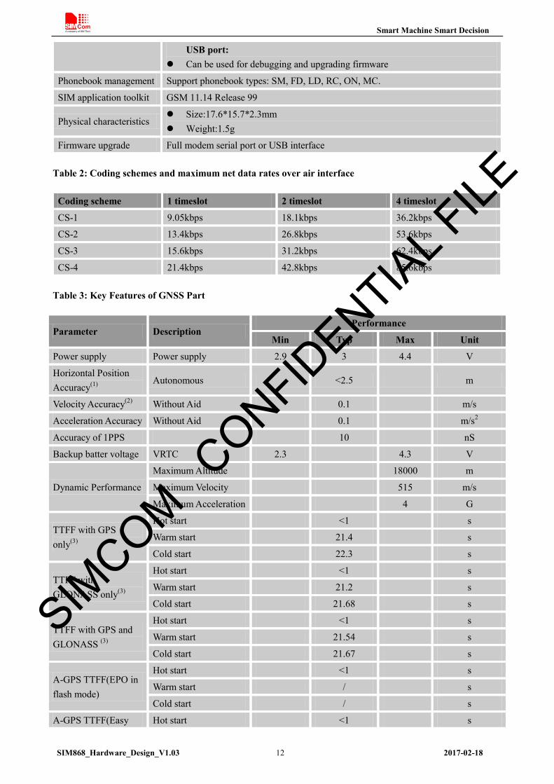
Table 2: Coding schemes and maximum net data rates over air interface
Coding scheme 1 timeslot 2 timeslot 4 timeslot
CS-1 9.05kbps 18.1kbps 36.2kbps
CS-2 13.4kbps 26.8kbps 53.6kbps
CS-3 15.6kbps 31.2kbps 62.4kbps
CS-4 21.4kbps 42.8kbps 85.6kbps
Table 3: Key Features of GNSS Part
Parameter Description Performance
Min Typ Max Unit
Power supply Power supply 2.9 3 4.4 V
Horizontal Position Accuracy(1)
Autonomous <2.5 m
Velocity Accuracy(2) Without Aid 0.1 m/s
Acceleration Accuracy Without Aid 0.1 m/s2
Accuracy of 1PPS 10 nS
Backup batter voltage VRTC 2.3 4.3 V
Dynamic Performance
Maximum Altitude 18000 m
Maximum Velocity 515 m/s
Maximum Acceleration 4 G
TTFF with GPS only(3)
Hot start <1 s
Warm start 21.4 s
Cold start 22.3 s
TTFF with GLONASS only(3)
Hot start <1 s
Warm start 21.2 s
Cold start 21.68 s
TTFF with GPS and GLONASS (3)
Hot start <1 s
Warm start 21.54 s
Cold start 21.67 s
A-GPS TTFF(EPO in flash mode)
Hot start <1 s
Warm start / s
Cold start / s
A-GPS TTFF(Easy Hot start <1 s
SIMCOM C
ONFIDENTIA
L FILE

Smart Machine Smart Decision
SIM868_Hardware_Design_V1.03 13 2017-02-18
mode) Warm start 1.4 s
Cold start 13.6 s
Sensitivity with GPS only mode
Autonomous acquisition(cold start)
-149
dBm
Re-acquisition -161 dBm
Tracking -167 dBm
Sensitivity with GLONASS only mode
Autonomous acquisition(cold start)
-147
dBm
Re-acquisition -155 dBm
Tracking -160 dBm
Sensitivity with GPS and GLONASS
Autonomous acquisition(cold start)
-149
dBm
Re-acquisition -161 dBm
Tracking -167 dBm
Receiver
Channels 33/99
Update rate 10 Hz
Tracking L1, CA Code
Protocol support NMEA
Power consumption With GPS only mode(4)
Acquisition 24.5 mA
Continuous tracking 22.2 mA
GLP current 12 mA
Sleep current 6.5 mA
Stop current 490 uA
Backup current 8 uA
Power consumption With BD only mode(4)
Acquisition 31 mA
Continuous tracking 31.2 mA
GLP current 12 mA
Sleep current 6.5 mA
Stop current 490 uA
Backup current 8 uA
Power consumption With GLONASS only mode(4)
Acquisition 22.4 mA
Continuous tracking 27.3 mA
GLP current 12 mA
Sleep current 6.5 mA
Stop current 490 uA
Backup current 8 uA
Power consumption With GPS and GLONASS (4)
Acquisition 31 mA
Continuous tracking 26 mA
GLP current 12 mA
Sleep current 6.5 mA
Stop current 590 uA
SIMCOM C
ONFIDENTIA
L FILE

Smart Machine Smart Decision
SIM868_Hardware_Design_V1.03 14 2017-02-18
Backup current 8 uA
Power consumption With GPS and BD (4)
Acquisition 31.2 mA
Continuous tracking 25.8 mA
GLP current 12 mA
Sleep current 6.5 mA
Stop current 490 uA
Backup current 8 uA
(1) 50% 24hr static, -130dBm (2) 50% at 30m/s (3) GPS signal level: -130dBm (4) Single Power supply 3V@-130dBm
2.2. Operating Modes
Table 4 summarizes the various operating modes of GSM:
Table 4: Overview of GSM operating modes
Mode Function
Normal operation
GSM/GPRS SLEEP
Module will automatically go into sleep mode if the conditions of sleep mode are enabling and there aren’t on air and hardware interrupt (such as GPIO interrupt or data on serial port). In this case, the current consumption of module will reduce to the minimal level. In sleep mode, the module can still receive paging message and SMS.
GSM IDLE Software is active. Module is registered to the GSM network and ready to communicate.
GSM TALK Connection between two subscribers is in progress. In this case, the power consumption depends on network settings such as DTX off/on, FR/EFR/HR, hopping sequences and antenna.
GPRS STANDBY
Module is ready for GPRS data transfer, but no data is currently sent or received. In this case, power consumption depends on network settings and GPRS configuration.
GPRS DATA
There is GPRS data transfer (PPP or TCP or UDP) in progress. In this case, power consumption is related with network settings (e.g. power control level); uplink/downlink data rates and GPRS configuration (e.g. used multi-slot settings).
Power off
Normal power off by sending AT command “AT+CPOWD=1” or using the PWRKEY. The power management unit shuts down the power supply for the baseband part of the module. Software is not active. The serial port is not accessible. Power supply (connected to 3V) remains applied.
Minimum functionality mode
AT command “AT+CFUN” can be used to set the module to a minimum functionality mode without removing the power supply. In this mode, the RF part of the module will not work or the SIM card will not be accessible, or both RF part and SIM card will be closed, and the serial port is still accessible. The power consumption in this mode is lower than normal mode.
SIMCOM C
ONFIDENTIA
L FILE

Smart Machine Smart Decision
SIM868_Hardware_Design_V1.03 15 2017-02-18
Table 5: Overview of GNSS operating modes
Note: X means no matter GPS_VBAT is existed or not.
2.3. Functional Diagram
Figure 1 shows the block diagram of SIM868: GSM baseband PMU The GSM Radio Frequency part Antenna interface GNSS interface Other interface
Figure 1: SIM868 block diagram
Mode GPS_VBAT GNSS_EN VRTC Main clock RTC clock
Full on on H on on on
Stop on H on off on
Backup X L on off on
SIMCOM C
ONFIDENTIA
L FILE

Smart Machine Smart Decision
SIM868_Hardware_Design_V1.03 16 2017-02-18
3. Package Information
3.1. Pin Out Diagram
MCCK
UART1_DTR
USB_DP
GPS_VBATGSM_VBATADC
UART1_RXD
PWRKEY
UART1_CTS
UART1_TXD
UART1_RTS
SCL SDA
UART1_DCD
NETLIGHT
SIM1_RSTSIM1_CLKSIM1_DET SIM1_DATA BT_ANT
SIM2_CLKSIM2_DET SIM2_DATA SIM2_RST SIM2_VDD
UART2_TXD
SPK1P
VRTC
MICP
MICN USB_VBUS
USB_DM
GSM_ANT
STATUS
SIM1_VDD
MCCA3
GND
UART2_RXD
GND
GPS_RXD
GNSS_EN
1PPS
GPIO2
GPS_TXD
13
SPK1N
UART1_RI
GPS_ANT
14 15 16 2117 18 19 20
22
23
24
25
26
27
28
29
30
31
32
33
37 36 35 34
1
42 41 40 39 38
5
4
2
3
6
11
10
9
8
7
51125352 5554 5756
58
62
61
60
59
67 66 65 64 63
46
45
44
43
49
48
47
50
VDD_EXT
GND
GND
GND
GND
GND
GND
GPIO1
GND
GND
GND
GND
UART1_DTR
RF_SYNC
GND
GND
SPK2P
68
MCCM0
MCCA1
SPK2N
MCCA2
MCCA0
GND GNDGND
GNDGNDGND
GNDGNDGND
7669 75
70 77 74
71 72 73
Figure 2: Pin out Diagram (Top view)
SIMCOM C
ONFIDENTIA
L FILE
Smart Machine Smart Decision
SIM868_Hardware_Design_V1.03 17 2017-02-18
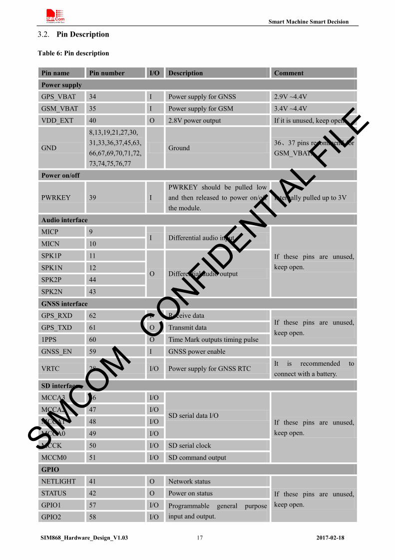
3.2. Pin Description
Table 6: Pin description
Pin name Pin number I/O Description Comment
Power supply
GPS_VBAT 34 I Power supply for GNSS 2.9V ~4.4V
GSM_VBAT 35 I Power supply for GSM 3.4V ~4.4V
VDD_EXT 40 O 2.8V power output If it is unused, keep open.
GND
8,13,19,21,27,30, 31,33,36,37,45,63,66,67,69,70,71,72,73,74,75,76,77
Ground 36、37 pins recommend for GSM_VBAT.
Power on/off
PWRKEY 39 I PWRKEY should be pulled low and then released to power on/off the module.
Internally pulled up to 3V
Audio interface
MICP 9 I Differential audio input
If these pins are unused, keep open.
MICN 10
SPK1P 11
O Differential audio output SPK1N 12
SPK2P 44
SPK2N 43
GNSS interface
GPS_RXD 62 I Receive data If these pins are unused, keep open.
GPS_TXD 61 O Transmit data
1PPS 60 O Time Mark outputs timing pulse
GNSS_EN 59 I GNSS power enable
VRTC 28 I/O Power supply for GNSS RTC It is recommended to connect with a battery.
SD interface
MCCA3 46 I/O
SD serial data I/O If these pins are unused, keep open.
MCCA2 47 I/O
MCCA1 48 I/O
MCCA0 49 I/O
MCCK 50 I/O SD serial clock
MCCM0 51 I/O SD command output
GPIO
NETLIGHT 41 O Network status
If these pins are unused, keep open.
STATUS 42 O Power on status
GPIO1 57 I/O Programmable general purpose input and output. GPIO2 58 I/O
SIMCOM C
ONFIDENTIA
L FILE
Smart Machine Smart Decision
SIM868_Hardware_Design_V1.03 18 2017-02-18
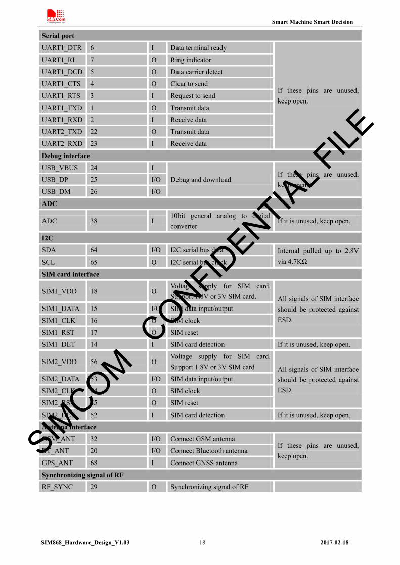
Serial port
UART1_DTR 6 I Data terminal ready
If these pins are unused, keep open.
UART1_RI 7 O Ring indicator
UART1_DCD 5 O Data carrier detect
UART1_CTS 4 O Clear to send
UART1_RTS 3 I Request to send
UART1_TXD 1 O Transmit data
UART1_RXD 2 I Receive data
UART2_TXD 22 O Transmit data
UART2_RXD 23 I Receive data
Debug interface
USB_VBUS 24 I
Debug and download If these pins are unused, keep open.
USB_DP 25 I/O
USB_DM 26 I/O
ADC
ADC 38 I 10bit general analog to digital converter
If it is unused, keep open.
I2C
SDA 64 I/O I2C serial bus data Internal pulled up to 2.8V via 4.7KΩ SCL 65 O I2C serial bus clock
SIM card interface
SIM1_VDD 18 O Voltage supply for SIM card. Support 1.8V or 3V SIM card. All signals of SIM interface
should be protected against ESD.
SIM1_DATA 15 I/O SIM data input/output
SIM1_CLK 16 O SIM clock
SIM1_RST 17 O SIM reset
SIM1_DET 14 I SIM card detection If it is unused, keep open.
SIM2_VDD 56 O Voltage supply for SIM card. Support 1.8V or 3V SIM card All signals of SIM interface
should be protected against ESD.
SIM2_DATA 53 I/O SIM data input/output
SIM2_CLK 54 O SIM clock
SIM2_RST 55 O SIM reset
SIM2_DET 52 I SIM card detection If it is unused, keep open.
Antenna interface
GSM_ANT 32 I/O Connect GSM antenna If these pins are unused, keep open.
BT_ANT 20 I/O Connect Bluetooth antenna
GPS_ANT 68 I Connect GNSS antenna
Synchronizing signal of RF
RF_SYNC 29 O Synchronizing signal of RF
SIMCOM C
ONFIDENTIA
L FILE
Smart Machine Smart Decision
SIM868_Hardware_Design_V1.03 19 2017-02-18
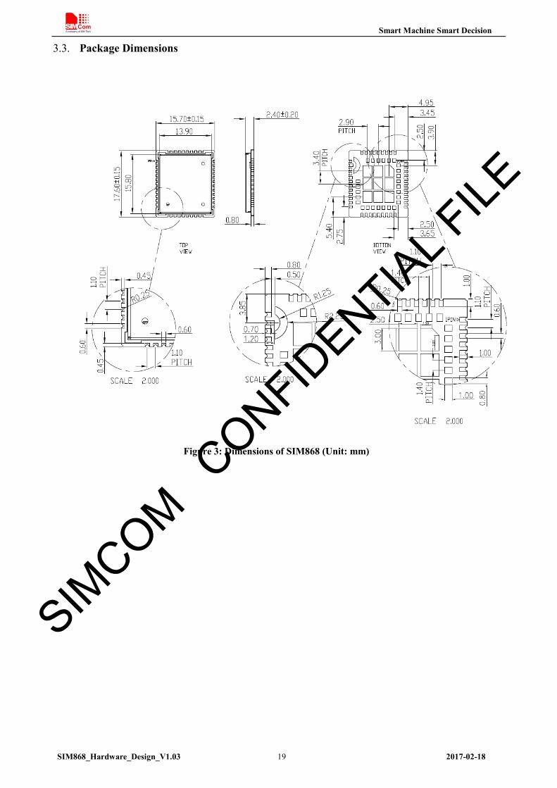
3.3. Package Dimensions
Figure 3: Dimensions of SIM868 (Unit: mm)
SIMCOM C
ONFIDENTIA
L FILE

Smart Machine Smart Decision
SIM868_Hardware_Design_V1.03 20 2017-02-18
Figure 4: Recommended PCB footprint outline
SIMCOM C
ONFIDENTIA
L FILE
Smart Machine Smart Decision
SIM868_Hardware_Design_V1.03 21 2017-02-18
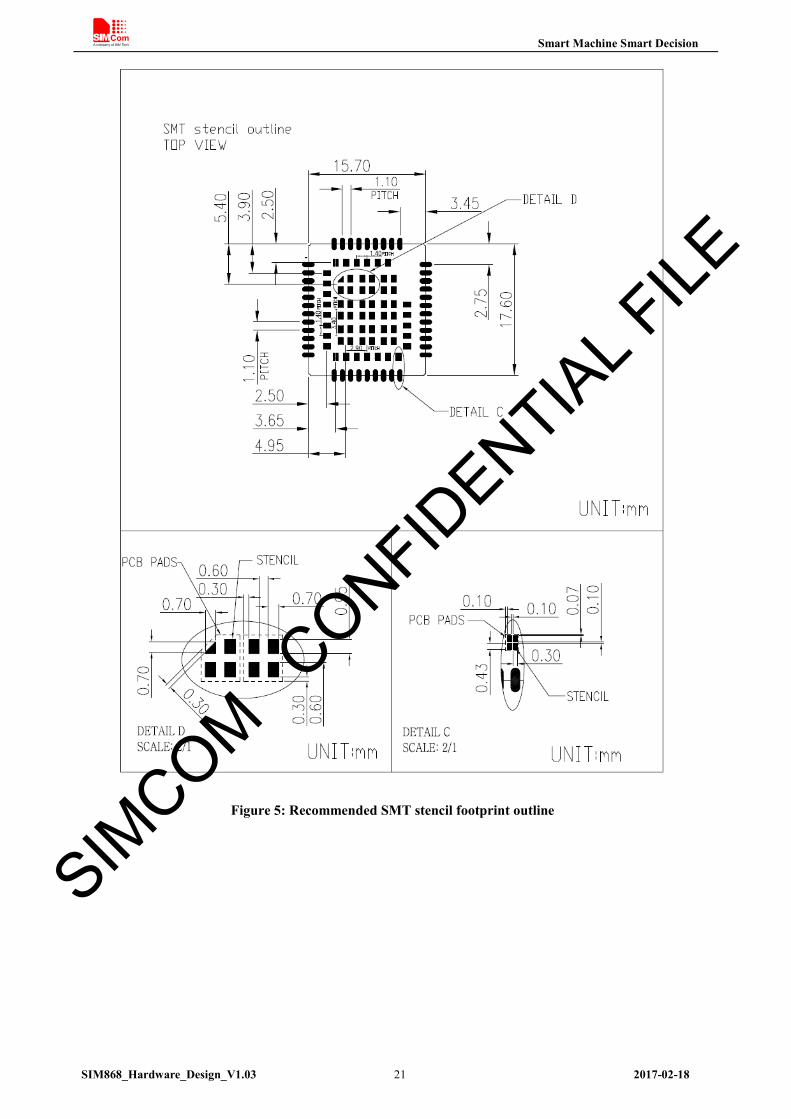
Figure 5: Recommended SMT stencil footprint outline
SIMCOM C
ONFIDENTIA
L FILE

Smart Machine Smart Decision
SIM868_Hardware_Design_V1.03 22 2017-02-18
4. Application Modes of SIM868
4.1. All-in-one Mode
In all-in-one mode, UART2 of GSM is connected with GNSS_UART. It’s convenient for communication between GSM and GNSS, such as control GNSS, firmware upgrade and download EPO data. As the Figure 6, a 10K resistor should be added between GPIO1 and GNSS_EN pin. In this mode, GNSS part can be enabled through AT command“AT+CGNSPWR=1”and disabled through AT command“AT+CGNSPWR=0”. GSM and GNSS’s firmware could be upgraded through UART1 port or USB with high-speed.
Module
GNSS_RXD
GNSS_TXD
UART2_RXD
UART2_TXD
VRTC VRTC
MCU
UAR
T1_T
XD
UAR
T1_R
XD
RXD TX
D
GSM_VBAT
LDOAdapter5V 4V
GPS_VBAT
GNSS_EN
OUT
PWR
KEY
V_GPSLDO
R10110K
GPIO1
USB
Figure 6: All-in-one Mode Diagram
SIMCOM C
ONFIDENTIA
L FILE

Smart Machine Smart Decision
SIM868_Hardware_Design_V1.03 23 2017-02-18
4.2. Stand-alone Mode
In stand-alone mode, GSM and GNSS part can work independently. It’s convenient for customer to control them separately. Figure 7 is the block diagram of this mode.
Module
VRTC VRTC
PWR
KEY
MCU
UAR
T1_T
XD
UAR
T1_R
XD
RXD
1
TXD
1
GSM_VBATLDOAdapter5V 4V
GN
SS_T
XD
GN
SS_R
XD
RXD
2
TXD
2
GPS_VBAT
GNSS_EN
OUTV_GPS
LDO
Figure 7: Stand-alone Mode Diagram
SIMCOM C
ONFIDENTIA
L FILE
Smart Machine Smart Decision
SIM868_Hardware_Design_V1.03 24 2017-02-18
5. Application Interface of GSM
5.1. Power Supply of GSM
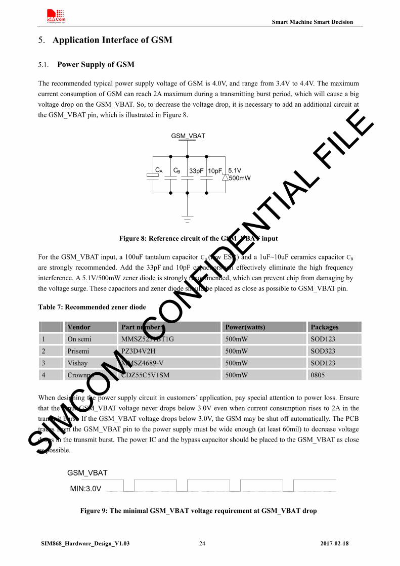
The recommended typical power supply voltage of GSM is 4.0V, and range from 3.4V to 4.4V. The maximum current consumption of GSM can reach 2A maximum during a transmitting burst period, which will cause a big voltage drop on the GSM_VBAT. So, to decrease the voltage drop, it is necessary to add an additional circuit at the GSM_VBAT pin, which is illustrated in Figure 8.
GSM_VBAT
5.1V500mW
CA CB 33pF 10pF
Figure 8: Reference circuit of the GSM_VBAT input
For the GSM_VBAT input, a 100uF tantalum capacitor CA (low ESR) and a 1uF~10uF ceramics capacitor CB are strongly recommended. Add the 33pF and 10pF capacitors can effectively eliminate the high frequency interference. A 5.1V/500mW zener diode is strongly recommended, which can prevent chip from damaging by the voltage surge. These capacitors and zener diode should be placed as close as possible to GSM_VBAT pin.
Table 7: Recommended zener diode
Vendor Part number Power(watts) Packages
1 On semi MMSZ5231BT1G 500mW SOD123
2 Prisemi PZ3D4V2H 500mW SOD323
3 Vishay MMSZ4689-V 500mW SOD123
4 Crownpo CDZ55C5V1SM 500mW 0805
When designing the power supply circuit in customers’ application, pay special attention to power loss. Ensure that the input GSM_VBAT voltage never drops below 3.0V even when current consumption rises to 2A in the transmit burst. If the GSM_VBAT voltage drops below 3.0V, the GSM may be shut off automatically. The PCB traces from the GSM_VBAT pin to the power supply must be wide enough (at least 60mil) to decrease voltage drops in the transmit burst. The power IC and the bypass capacitor should be placed to the GSM_VBAT as close as possible.
GSM_VBAT
MIN:3.0V
Figure 9: The minimal GSM_VBAT voltage requirement at GSM_VBAT drop
SIMCOM C
ONFIDENTIA
L FILE
Smart Machine Smart Decision
SIM868_Hardware_Design_V1.03 25 2017-02-18
5.2. Reference Circuit of GSM Power Supply
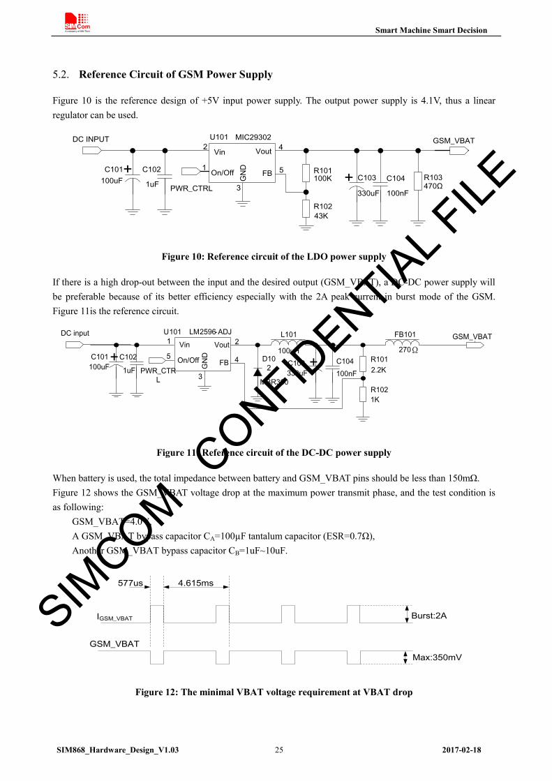
Figure 10 is the reference design of +5V input power supply. The output power supply is 4.1V, thus a linear regulator can be used.
Vin Vout
GND FB
3
+PWR_CTRL
R102
R101
GSM_VBAT
100K
43K
+ C103
330uF
C104
100nF
U101 MIC29302
5
4
1
2
C101 C102100uF 1uF
DC INPUT
R103470Ω
On/Off
Figure 10: Reference circuit of the LDO power supply
If there is a high drop-out between the input and the desired output (GSM_VBAT), a DC-DC power supply will be preferable because of its better efficiency especially with the 2A peak current in burst mode of the GSM. Figure 11is the reference circuit.
Vin Vout
FB
U1011 2
3
45
LM2596-ADJ
+100uH
MBR360
L101
C101 +C102 D102 C103
R102
R101
FB101
330uF
GSM_VBAT
2.2K
1K
100uF 1uFC104100nF
270
DC input
PWR_CTRL
GN
D ΩOn/Off
Figure 11: Reference circuit of the DC-DC power supply
When battery is used, the total impedance between battery and GSM_VBAT pins should be less than 150mΩ. Figure 12 shows the GSM_VBAT voltage drop at the maximum power transmit phase, and the test condition is as following:
GSM_VBAT=4.0V, A GSM_VBAT bypass capacitor CA=100µF tantalum capacitor (ESR=0.7Ω), Another GSM_VBAT bypass capacitor CB=1uF~10uF.
577us 4.615ms
Burst:2AIGSM_VBAT
GSM_VBATMax:350mV
Figure 12: The minimal VBAT voltage requirement at VBAT drop
SIMCOM C
ONFIDENTIA
L FILE
Smart Machine Smart Decision
SIM868_Hardware_Design_V1.03 26 2017-02-18
5.3. Power on/off GSM Part
5.3.1. Power on GSM
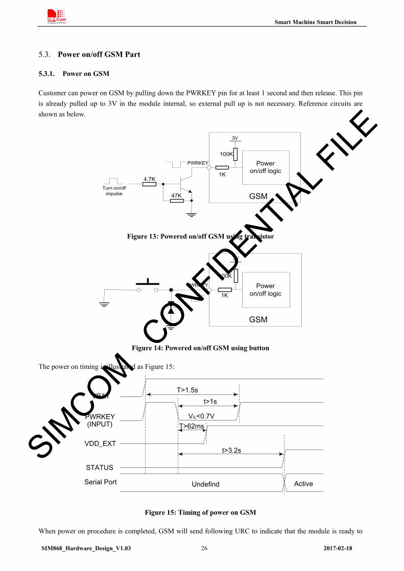
Customer can power on GSM by pulling down the PWRKEY pin for at least 1 second and then release. This pin is already pulled up to 3V in the module internal, so external pull up is not necessary. Reference circuits are shown as below.
4.7K
47KTurn on/off
impulse
PWRKEY Power on/off logic
100K
3V
GSM
1K
Figure 13: Powered on/off GSM using transistor
PWRKEY Power on/off logic
100K
3V
GSM
1K
Figure 14: Powered on/off GSM using button
The power on timing is illustrated as Figure 15:
VIL<0.7V
Undefind Active
VBAT
PWRKEY(INPUT)
t>3.2sVDD_EXT
STATUS
t>1s
Serial Port
T>1.5s
T>62ms
Figure 15: Timing of power on GSM
When power on procedure is completed, GSM will send following URC to indicate that the module is ready to
SIMCOM C
ONFIDENTIA
L FILE

Smart Machine Smart Decision
SIM868_Hardware_Design_V1.03 27 2017-02-18
operate at fixed baud rate. RDY
This URC does not appear when autobauding function is active.
Note: Customer can use AT command “AT+IPR=x” to set a fixed baud rate and save the configuration to non-volatile flash memory. After the configuration is saved as fixed baud rate, the Code “RDY” should be received from the serial port every time when SIM868 is powered on. For details, please refer to the chapter “AT+IPR” in document [1].
5.3.2. Power off GSM
GSM will be powered off in the following situations: Power off GSM by the PWRKEY pin. Power off GSM by AT command “AT+CPOWD=1”.
5.3.2.1. Power off GSM by the PWRKEY Pin
Customer can power off GSM by pulling down the PWRKEY pin for at least 1.5 second and release. The power off timing is illustrated in Figure 16.
PWRKEY
VDD_EXT
STATUS
VIL<0.7V
Serial port UndifinedActive
(input)
T3=2s
1.5s<T1<33s
T2≥2s
Figure 16: Timing of power off GSM
Note: 1. The GSM will restart after pulling down the PWRKEY over 33 seconds. 2. VDD_EXT will power off after STATUS changes into low level and the PWRKEY release 55ms.
If 1.5s<T1<2s,T2>2s; If 2s≤T1<33s,T2>T1+55ms
This procedure makes the GSM log off from the network and allows the software to enter into a secure state to save data before completely shut off. Before the completion of the power off procedure, the GSM will send URC:
NORMAL POWER OFF At this moment, AT commands can’t be executed any more. Power off mode can also be indicated by STATUS pin, which is at low level at this time.
5.3.2.2. Power off GSM by AT Command
GSM can be powered off by AT command “AT+CPOWD=1”. This procedure makes the GSM log off from the network and allows the software to enter into a secure state to save data before completely shut off. Before the completion of the power off procedure, the GSM will send URC:
SIMCOM C
ONFIDENTIA
L FILE

Smart Machine Smart Decision
SIM868_Hardware_Design_V1.03 28 2017-02-18
NORMAL POWER OFF At this moment, AT commands can’t be executed any more. Power off mode can also be indicated by STATUS pin, which is at low level at this time. For detail about AT command “AT+CPOWD”, please refer to document [1].
5.3.2.3. Restart GSM by PWRKEY:
When the GSM works normally, if the customer wants to restart the GSM, follow the procedure as Figure 17: 1) Power off the GSM. 2) Wait for at least 800ms after STATUS pin changes to low level. 3) Power on the GSM.
PWRKEY
T2≥2sSTATUS
T3>800ms1.5s<T1<2s
Figure 17: Timing of restart GSM
5.4. Power Saving Mode of GSM
GSM has two power saving modes: Minimum functionality mode and sleep mode. AT command “AT+CSCLK=1”can be used to set GSM into sleep mode. AT command “AT+CFUN=<fun>“can be used to set GSM into minimum functionality. When GSM is in sleep mode and also in minimum functionality mode, the current of GSM is the lowest.
5.4.1. Minimum Functionality Mode of GSM Part
There are three functionality modes, which could be set by AT command “AT+CFUN=<fun>“. The command provides the choices of the functionality levels <fun>=0, 1, 4. AT+CFUN=0: Minimum functionality AT+CFUN=1: Full functionality (default) AT+CFUN=4: Flight mode (disable RF function)
Table 8: The current consumption of Function Mode
<fun> BS-PA-MFRMS Current consumption(mA)
0 / 0.65
1
9 0.86
5 1.02
2 1.42
4 / 0.69
Minimum functionality mode minimizes the current consumption to the lowest level. If GSM is set to minimum functionality mode by “AT+CFUN=0”, the RF function and SIM card function will be disabled. In
SIMCOM C
ONFIDENTIA
L FILE

Smart Machine Smart Decision
SIM868_Hardware_Design_V1.03 29 2017-02-18
this case, the serial port is still accessible, but partial AT commands and correlative to RF function and SIM card function will not be accessible. For detailed information about AT command “AT+CFUN=<fun>“, please refer to document [1].
5.4.1.1. Sleep Mode 1 (AT+CSCLK=1)
Customer can control GSM to enter or exit the sleep mode (AT+CSCLK=1) by DTR signal. When DTR is in high level and without interrupt (on air and hardware such as GPIO interrupt or data in serial port), GSM will enter sleep mode automatically. In this mode, GSM can still receive paging or SMS from network but the serial port is not accessible.
5.4.1.2. Wake Up GSM from Sleep Mode 1
When GSM is in sleep mode 1(AT+CSCLK=1), the following methods can wake up the GSM: Pull down DTR pin The serial port will be active after DTR pin is pulled to low level for about 50ms Receive a voice or data call from network Receive a SMS from network Receive external interrupt
Note: After module has received incoming call or new SMS, serial port can report URC, but it cannot input AT command. Only after the DTR pin is pulled to low level for 50ms, the serial port can input AT command.
5.4.1.3. Sleep Mode 2 (AT+CSCLK=2)
In this mode, GSM will continuously monitor the serial port data signal. When there is no data transfer over 5 seconds on the RXD signal and there is no on air and hardware interrupts (such as GPIO interrupt), GSM will enter sleep mode 2 automatically. In this mode, GSM can still receive paging or SMS from network.
5.4.1.4. Wake Up GSM from Sleep Mode 2
When GSM is in sleep mode 2 (AT+CSCLK=2), the following methods can wake up the module: Send data to GSM via main serial port (the first character will lose). Receive a voice or data call from network. Receive a SMS from network. Note: Autobauding is default. It cannot enter sleep mode in the absence of synchronous serial port baud rate after GSM power on.
5.5. Serial Port of GSM
GSM default provides one unbalanced asynchronous serial port and one three-line serial port.
Table 9: Serial port pin definition
Pin name Pin number Function
Serial port
UART1_DTR 6 Data terminal ready
UART1_RI 7 Ring indicator
UART1_DCD 5 Data carrier detect
UART1_CTS 4 Clear to send
UART1_RTS 3 Request to send
SIMCOM C
ONFIDENTIA
L FILE

Smart Machine Smart Decision
SIM868_Hardware_Design_V1.03 30 2017-02-18
Note: Hardware flow control is disabled by default. AT command “AT+IFC=2, 2”can enable hardware flow control. AT command “AT+IFC=0,0”can disable hardware flow control. For more details please refer to document [1].
Table 10: Serial port characteristics
Symbol Min Max Unit
VIL -0.3 0.7 V
VIH 2.1 3.0 V
VOL - 0.4 V
VOH 2.4 - V
5.5.1. Function of Serial Port
Serial port: Full mode device. Contain data lines UART1_TXD/UART1_RXD; hardware flow control lines UART1_RTS/UART1_CTS,
status lines UART1_DTR, UART1_DCD and UART1_RI. Serial port can be used for GPRS service and AT communication. Autobauding supports the following baud rates:
1200, 2400, 4800, 9600, 19200, 38400, 57600 and 115200bps Autobauding allows GSM to automatically detect the baud rate of the host device. Pay more attention to the following requirements: Synchronization between DTE and DCE:
When DCE powers on with autobauding enabled, it is recommended to send "AT" or "at" or "aT" or "At" to synchronize the baud rate, until DTE receives the "OK" response, which means DTE and DCE are correctly synchronized. For more information please refer to AT command "AT+IPR".
Restrictions of autobauding operation: The DTE serial port must be set at 8 data bits, no parity and 1 stop bit. The URC such as "RDY", "+CFUN: 1" and "+CPIN: READY” will not be reported.
Note: Customer can use AT command “AT+IPR=x” to set a fixed baud rate and the setting will be saved to non-volatile flash memory automatically. After the configuration is set as fixed baud rate, the URC such as "RDY", "+CFUN: 1" and "+CPIN: READY” will be reported when GSM is powered on.
5.5.2. Serial Interfaces
The following figure shows the connection between GSM and client (DTE).
UART1_TXD 1 Transmit data
UART1_RXD 2 Receive data
UART2_TXD 22 Transmit data
UART2_RXD 23 Receive data
SIMCOM C
ONFIDENTIA
L FILE

Smart Machine Smart Decision
SIM868_Hardware_Design_V1.03 31 2017-02-18
UART1_TXD
UART1_RXD
UART1_RTS
UART1_CTS
UART1_DTR
UART1_DCD
UART1_RI
TXD
RXD
RTS
CTS
DTR
DCD
RING
Serial Port Serial PortGSM(DCE) Customer(DTE)
GND GND
Figure 18: Connection of the serial interfaces
If the voltage of UART is 3.3V, the following reference circuits are recommended. If the voltage is 3.0V, please change the resistors in the following figure from5.6K to 14K.
1K
5.6K
RXD
TXD
RTS
CTS
GPIO
GPIO
EINT
DTE(3.3V)
5.6K5.6K
1K
1K
1K
1K
1K
1K
GSM
UART1_TXD
UART1_RXD
UART1_RTS
UART1_CTS
UART1_DTR
UART1_DCD
UART1_RI
GND GND
Figure 19: Resistor matching circuit
If the voltage of UART is 3V or3.3V, the following reference circuit is recommended:
UART1_TXD RXD
GSM DTE
TXDUART1_RXD
VDD_EXT10K
10K
GND GND
Figure 20 : Diode isolation circuit
Note: Please make sure the minimum of client high limit should be less than 2.8V minus the diode drop. If the voltage of UART is 5V, the following reference circuit is recommended:
SIMCOM C
ONFIDENTIA
L FILE

Smart Machine Smart Decision
SIM868_Hardware_Design_V1.03 32 2017-02-18
VDD_EXT
4.7K
47K
UART1_TXD
4.7K
GSM
VDD_EXT
RXD
VDD
DTE
Figure 21: TX level matching circuit
VDD_EXT
4.7K
47K4.7K
DTE
UART1_RXD
GSM
VDD_EXT
TXD
VDD
Figure 22: RX level matching circuit
5.5.3. Debug Interface
GSM could be debugged through USB port. The recommended diagram is shown as Figure 23:
GSM USB
GNDGND
22R
USB_VBUS VBUS
1uF
USB_DM
USB_DP
USB_DM22R
USB_DP
Figure 23: USB reference circuit
The TVS on USB data line should be less than 5pF, and the USB signals have to be layout according to differential signal layout rules. Note: Please reserve the USB interface or test point for further debugging.
SIMCOM C
ONFIDENTIA
L FILE

Smart Machine Smart Decision
SIM868_Hardware_Design_V1.03 33 2017-02-18
Table 11: USB_VBUS operation voltage
Pin Min Typ Max Unit
USB_VBUS 4.3 5.0 7.0 V
5.5.4. Software Upgrade of GSM
Customer could upgrade module’s GSM part firmware through USB or UART interface. If upgrading GSM part through USB interface, it is necessary to connect USB_VBUS, USB_DP, USB_DM, and GND to PC. There is no need to operate PWRKEY pin in the whole procedure, when GSM detects USB_VBUS and can communicate normally with USB_DP and USB_DM, it will enter USB download mode automatically. If customer upgrades GSM through UART interface, it is strongly recommended to lead the UART1_TXD, UART1_RXD, GND and PWRKEY pin to IO connector for the upgrading, and PWRKEY pin should be connected to GND while upgrading. Refer to Figure 24 for debugging and upgrading software.
UART1_TXD
GSM(DCE)
UART1_RXD
GND
PWRKEY
TXD
RXD
GND
Serial Port
PWRKEY
I/O Connector
Figure 24: Connection for software upgrading
The UART interface supports the CMOS level. If customer connects the module to the computer, the level shift should be added between the DCE and DTE.
5.6. UART1_RI Behaviors
Table 12: UART_RI behaviours
State RI response
Standby High
Voice call
The pin is changed to low. When any of the following events occur, the pin will be changed to high: (1)Establish the call (2)Hang up the call
SMS The pin is changed to low, and kept low for 120ms when a SMS is received. Then it is changed to high.
Others For more details, please refer to document [2].
SIMCOM C
ONFIDENTIA
L FILE
Smart Machine Smart Decision
SIM868_Hardware_Design_V1.03 34 2017-02-18
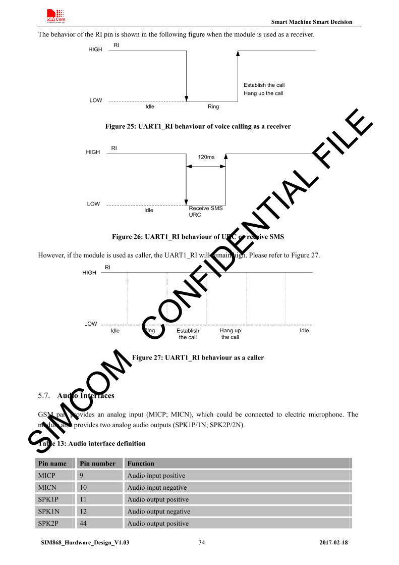
The behavior of the RI pin is shown in the following figure when the module is used as a receiver.
HIGH
LOWIdle Ring
Hang up the callEstablish the call
RI
Figure 25: UART1_RI behaviour of voice calling as a receiver
HIGH
LOWIdle
RI120ms
Receive SMSURC
Figure 26: UART1_RI behaviour of URC or receive SMS
However, if the module is used as caller, the UART1_RI will remain high. Please refer to Figure 27.
HIGH
LOWIdle Ring Establish
the callHang up the call
Idle
RI
Figure 27: UART1_RI behaviour as a caller
5.7. Audio Interfaces
GSM part provides an analog input (MICP; MICN), which could be connected to electric microphone. The module also provides two analog audio outputs (SPK1P/1N; SPK2P/2N).
Table 13: Audio interface definition
Pin name Pin number Function
MICP 9 Audio input positive
MICN 10 Audio input negative
SPK1P 11 Audio output positive
SPK1N 12 Audio output negative
SPK2P 44 Audio output positive
SIMCOM C
ONFIDENTIA
L FILE

Smart Machine Smart Decision
SIM868_Hardware_Design_V1.03 35 2017-02-18
SPK2N 43 Audio output negative
SPK1P/1N output can directly drive 32Ω receiver. SPK2P/2N output can directly drive 8Ω speaker, which integrates class-AB audio amplifier as shown Table 14:
Table 14: Performance of audio amplifier
Test Conditions Class-AB AMP
4.2V 8Ω THD+N=1% 0.87W
3.3V 8Ω THD+N=1% 0.53W
4.2V 8Ω THD+N=10% 1.08W
3.3V 8Ω THD+N=10% 0.65W
AT command “AT+CMIC” is used to adjust the input gain level of microphone. AT command “AT+SIDET” is used to set the side-tone level. In addition, AT command “AT+CLVL” is used to adjust the output gain level. For more details, please refer to document [1]. In order to improve audio performance, the following reference circuits are recommended. The audio signals have to be layout according to differential signal layout rules as shown in Figure 28 and Figure 29.
5.7.1. Speaker Interfaces Configuration
SPK1P/2P
Close to speaker
ESD
ESD
10pF
33pF
33pF
33pF
Module
SPK1N/2N
10pF
10pF
10pF
33pF
33pF
33pF
10pF
10pF
Figure 28: Speaker reference circuit
SIMCOM C
ONFIDENTIA
L FILE
Smart Machine Smart Decision
SIM868_Hardware_Design_V1.03 36 2017-02-18
5.7.2. Microphone Interfaces Configuration
Electret Microphone
The lines in bold type should be accorded to differential
signal layout rules
These components should be placed to microphone
as close as possible
MICP
Module
MICNESD
ESD
10pF
33pF
33pF
33pF
10pF
10pF
Figure 29: Microphone reference circuit
5.7.3. Audio Electronic Characteristic
Table 15: Microphone input characteristics
Parameter Min Typ Max Unit
Microphone biasing voltage - 1.9 2.2 V
Working current - - 2.0 mA
Input impedance(differential) 13 20 27 KΩ
Idle channel noise - - -67 dBm0
SINAD Input level:-40dBm0 29 - - dB
Input level:0dBm0 - 69 - dB
Table 16: Audio output characteristics
Parameter Conditions Min Typ Max Unit
Normal output RL=32 Ω receiver - 15 90 mW
RL=8 Ω speaker - - 1080 mW
5.7.4. TDD Noise of GSM
Audio signal could be interfered by RF signal. Coupling noise could be filtered by adding 33pF and 10pF capacitor to audio lines. 33pF capacitor could eliminate noise from GSM850/EGSM900MHz, while 10pF capacitor could eliminate noise from DCS1800/PCS1900Mhz frequency. Customer should adjust this filter solution according to field test result.
SIMCOM C
ONFIDENTIA
L FILE

Smart Machine Smart Decision
SIM868_Hardware_Design_V1.03 37 2017-02-18
GSM antenna is the key coupling interfering source of TDD noise. Thereat, pay attention to the layout of audio lines which should be far away from RF cable, antenna and GSM_VBAT pin. The bypass capacitor for filtering should be placed near module. Conducting noise is mainly caused by the GSM_VBAT drop. If audio PA is powered by GSM_VBAT directly, then there will be some cheep noise from speaker output easily. So it is better to put big capacitors and ferrite beads near audio PA input. TDD noise is related to GND signal. If GND plane is not good, lots of high-frequency noises will interfere microphone and speaker over bypass capacitor.
5.8. SIM Card Interface
The SIM interface complies with the GSM Phase 1 specification and the new GSM Phase 2+ specification for FAST 64kbps SIM card. Both 1.8V and 3.0V SIM card are supported. The SIM interface is powered from an internal regulator in the module.
5.8.1. SIM Card Application
Table 17: SIM pin definition
Pin name Pin number Function
SIM1_VDD 18 Voltage supply for SIM card. Support 1.8V or 3V SIM card
SIM1_DATA 15 SIM data input/output
SIM1_CLK 16 SIM clock
SIM1_RST 17 SIM reset
SIM1_DET 14 SIM card detection
SIM2_VDD 56 Voltage supply for SIM card. Support 1.8V or 3V SIM card
SIM2_DATA 53 SIM data input/output
SIM2_CLK 54 SIM clock
SIM2_RST 55 SIM reset
SIM2_DET 52 SIM card detection
It is recommended to use an ESD protection component such as ST (www.st.com ) ESDA6V1-5W6 or ON SEMI (www.onsemi.com ) SMF05C. The SIM card peripheral components should be placed close to the SIM card holder. The reference circuit of the 8-pin SIM card holder is illustrated in Figure 30.
SIMCOM C
ONFIDENTIA
L FILE
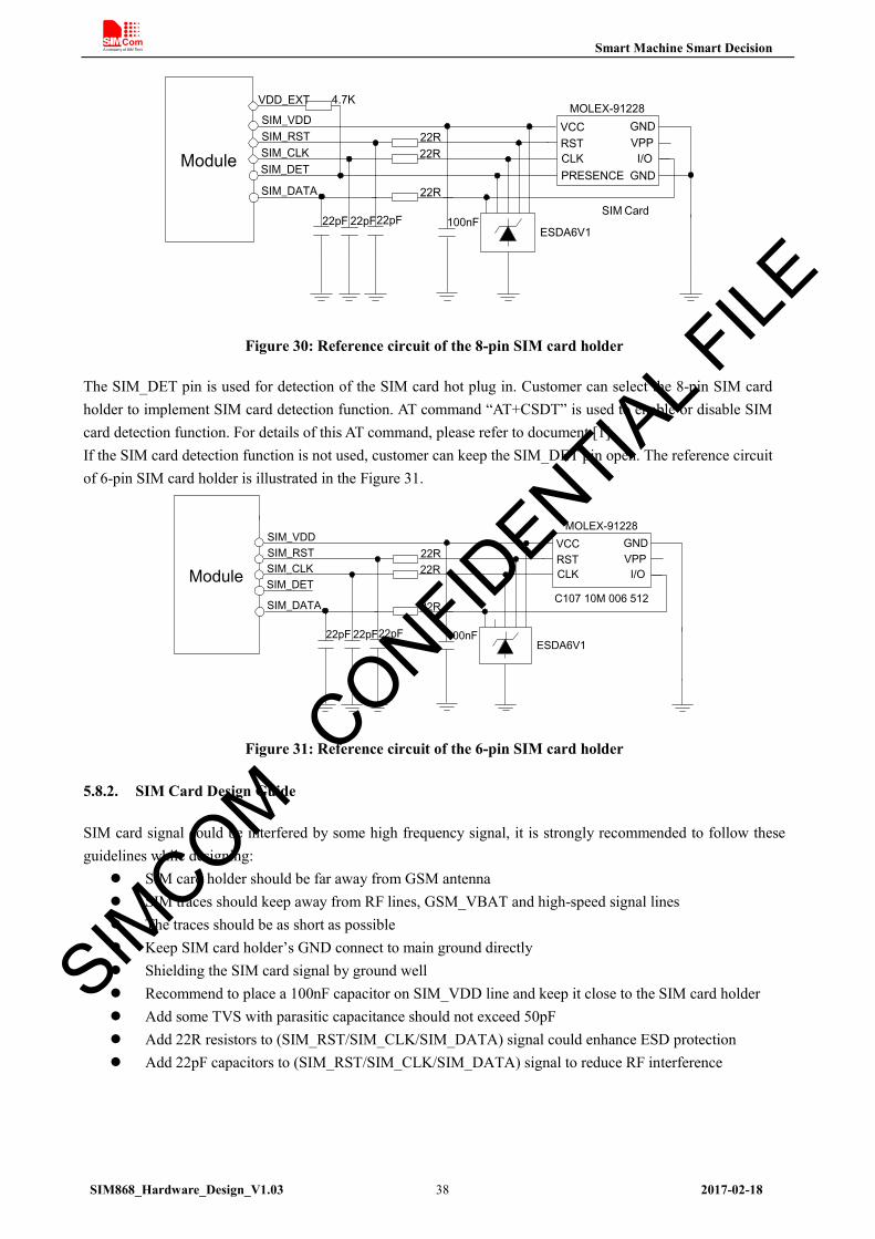
Smart Machine Smart Decision
SIM868_Hardware_Design_V1.03 38 2017-02-18
ModulePRESENCE
100nF
MOLEX-91228
SIM Card22pF
VCC GNDRST VPPCLK I/O
GND
VDD_EXTSIM_VDDSIM_RSTSIM_CLK
SIM_DATA
4.7K
ESDA6V1
SIM_DET
22R
22R
22pF
22R
22pF
Figure 30: Reference circuit of the 8-pin SIM card holder
The SIM_DET pin is used for detection of the SIM card hot plug in. Customer can select the 8-pin SIM card holder to implement SIM card detection function. AT command “AT+CSDT” is used to enable or disable SIM card detection function. For details of this AT command, please refer to document [1]. If the SIM card detection function is not used, customer can keep the SIM_DET pin open. The reference circuit of 6-pin SIM card holder is illustrated in the Figure 31.
Module
100nF
MOLEX-91228
C107 10M 006 512
22pF
VCC GNDRST VPPCLK I/O
SIM_VDDSIM_RSTSIM_CLK
SIM_DATA
ESDA6V1
SIM_DET
22R
22R
22pF
22R
22pF
Figure 31: Reference circuit of the 6-pin SIM card holder
5.8.2. SIM Card Design Guide
SIM card signal could be interfered by some high frequency signal, it is strongly recommended to follow these guidelines while designing: SIM card holder should be far away from GSM antenna SIM traces should keep away from RF lines, GSM_VBAT and high-speed signal lines The traces should be as short as possible Keep SIM card holder’s GND connect to main ground directly Shielding the SIM card signal by ground well Recommend to place a 100nF capacitor on SIM_VDD line and keep it close to the SIM card holder Add some TVS with parasitic capacitance should not exceed 50pF Add 22R resistors to (SIM_RST/SIM_CLK/SIM_DATA) signal could enhance ESD protection Add 22pF capacitors to (SIM_RST/SIM_CLK/SIM_DATA) signal to reduce RF interference
SIMCOM C
ONFIDENTIA
L FILE
Smart Machine Smart Decision
SIM868_Hardware_Design_V1.03 39 2017-02-18
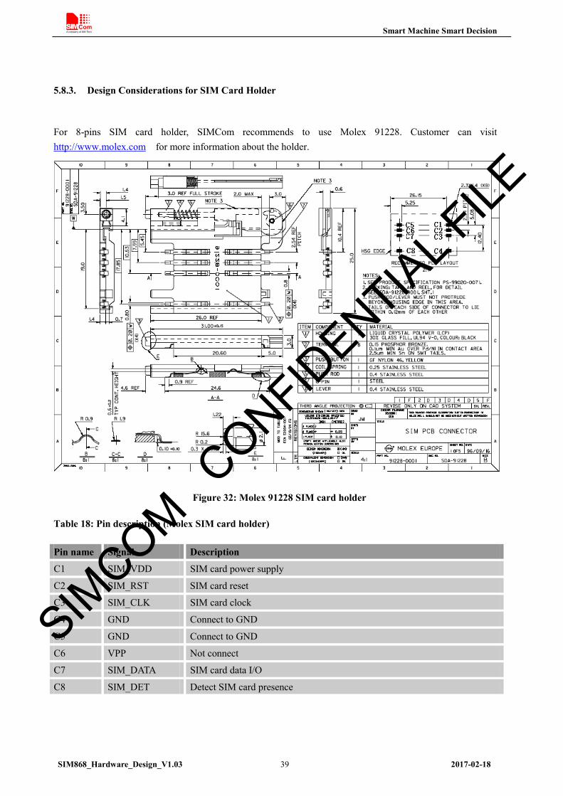
5.8.3. Design Considerations for SIM Card Holder
For 8-pins SIM card holder, SIMCom recommends to use Molex 91228. Customer can visit http://www.molex.com for more information about the holder.
Figure 32: Molex 91228 SIM card holder
Table 18: Pin description (Molex SIM card holder)
Pin name Signal Description
C1 SIM_VDD SIM card power supply
C2 SIM_RST SIM card reset
C3 SIM_CLK SIM card clock
C4 GND Connect to GND
C5 GND Connect to GND
C6 VPP Not connect
C7 SIM_DATA SIM card data I/O
C8 SIM_DET Detect SIM card presence
SIMCOM C
ONFIDENTIA
L FILE
Smart Machine Smart Decision
SIM868_Hardware_Design_V1.03 40 2017-02-18
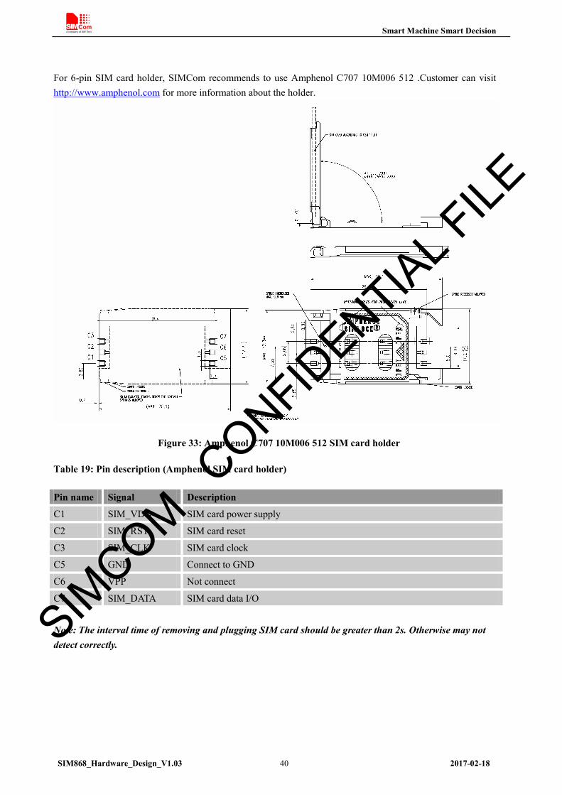
For 6-pin SIM card holder, SIMCom recommends to use Amphenol C707 10M006 512 .Customer can visit http://www.amphenol.com for more information about the holder.
Figure 33: Amphenol C707 10M006 512 SIM card holder
Table 19: Pin description (Amphenol SIM card holder)
Pin name Signal Description
C1 SIM_VDD SIM card power supply
C2 SIM_RST SIM card reset
C3 SIM_CLK SIM card clock
C5 GND Connect to GND
C6 VPP Not connect
C7 SIM_DATA SIM card data I/O
Note: The interval time of removing and plugging SIM card should be greater than 2s. Otherwise may not detect correctly. SIM
COM CONFID
ENTIAL F
ILE

Smart Machine Smart Decision
SIM868_Hardware_Design_V1.03 41 2017-02-18
5.9. SD Interface
The reference circuit is recommended in Figure 34:
Module SD
GND
DAT2
DAT3
CMD
VDD
CLK
DAT0
DAT1
MCCA2
MCCA3
MCCM0
VDD_SD
MCCK
GND
MCCA0
MCCA1
Figure 34: SD reference circuit
If the power supply is 2.8V for SD card, customer can use VDD_EXT; if the power supply is 3.3V, please use external LDO.
5.10. I2C Bus
The SIM868 provides an I2C interface which is only used in the embedded AT application.
Table 20: Pin definition of the I2C
Note: 1. I2C should be pulled up to 2.8V via 4.7K resistor externally. 2. I2C function is not supported in the standard firmware. If you need, please contact SIMCom.
5.11. ADC
Table 21: Pin definition of the ADC
SIM868 provides an auxiliary ADC, which can be used to measure the voltage. Customer can use AT command “AT+CADC” to read the voltage value. Note: Customer can use AT command set mode. For details, please refer to document [1].
Pin name Pin number Description
SCL 65 I2C serial bus clock(open drain output)
SDA 64 I2C serial bus data(open drain output)
Pin name Pin number Description
ADC 38 Analog voltage input SIM
COM CONFID
ENTIAL F
ILE

Smart Machine Smart Decision
SIM868_Hardware_Design_V1.03 42 2017-02-18
Table 22: ADC specification
Parameter Min Typ Max Unit
Voltage range 0 - 2.8 V
ADC Resolution - 10 - bits
Sampling rate - - 1.08 MHz
ADC precision 10 30 mV
5.12. Network Status Indication
Table 23: Pin definition of the NETLIGHT
The NETLIGHT pin can be used to drive a network status indication LED. The status of this pin is listed in following table:
Table 24: Status of the NETLIGHT
Status SIM868 behavior Off Powered off 64ms On/ 800ms Off Not registered the network 64ms On/ 3000ms Off Registered to the network 64ms On/ 300ms Off GPRS communication is established Reference circuit is recommended in Figure 35:
Module
NETLIGHT
GSM_VBAT
4.7K
47K
R
Figure 35: Reference circuit of NETLIGHT
Note: Customer can use AT command set mode. For details, please refer to document [1].
5.13. Operating Status Indication
The pin42 is for operating status indication of the module. The pin output is high when module is powered on
Pin name Pin number Description NETLIGHT 41 Network Status Indication
SIMCOM C
ONFIDENTIA
L FILE

Smart Machine Smart Decision
SIM868_Hardware_Design_V1.03 43 2017-02-18
and low when module is powered off.
Table 25: Pin definition of the STATUS
Pin name Pin number Description
STATUS 42 Operating status indication
Note: For timing about STATUS, please refer to the chapter “Power on/off GSM Part”
5.14. RF Synchronization Signal
The synchronization signal serves to indicate GSM transmit burst.
Table 26: Definition of the RF_SYNC pin
RF sync signal is raised to high level 220us prior to GSM transmit burst, and changed to low level at the end of the GSM transmit burst. The timing of the RF sync signal is shown in Figure 35.
Transmit burst
RF_SYNC
577us220us
Figure 36: RF_SYNC signal during transmit burst
5.15. Antenna Interface of GSM
Antenna interface of GSM: The input impendence of the antenna should be 50Ω, and the VSWR should be less than 2. It is recommended that the GSM antenna should be placed as far as possible. The isolation of the antenna should be bigger than 30dB
Note:About RF design, please refer to document [15], [16] for more information.
The GSM antenna pad named GSM_ANT which is connected to an external GSM antenna, the connection of the antenna must be decoupled from DC voltage. This is necessary because the antenna connector is DC coupled to ground via an inductor for ESD protection. The external antenna must be matched properly to achieve the best performance, so the matching circuit is necessary. It is recommended to reserve the matching circuit as following:
Pin name Pin number Description
RF_SYNC 29 Transmit synchronization signal
SIMCOM C
ONFIDENTIA
L FILE

Smart Machine Smart Decision
SIM868_Hardware_Design_V1.03 44 2017-02-18
Module
GND(Pin33)
RF connectorR101GSM_ANT
C101 C102
GND(Pin31)
GSMAntenna
(Pin32)
D101
Figure 37: GSM antenna matching circuit
The RF connector is used for conduction test. If the space between RF pin and antenna is not enough, the matching circuit should be designed as in the following figure:
ModuleR101GSM_ANT
C101 C102
GND(Pin33)
GND(Pin31)
GSMAntenna
(Pin32)D101
Figure 38: GSM antenna matching circuit without RF connector
In above figure, the components R101, C101 and C102 are used for antenna matching, the value of the components can only be got after the antenna tuning, usually, they are provided by antenna vendor. By default, the R101 is 0Ω resistor, and the C101, C102 are reserved for tuning. The RF test connector in the figure is used for the conducted RF performance test, and should be placed close to the module’s antenna pin. The traces impedance between components must be controlled in 50Ω.The component D101 is a bidirectional TVS component, which is used for ESD protection, the recommended part numbers of the TVS are listed in the Table 27:
Table 27: Recommended TVS component
Package Type Supplier
0201 LXES03AAA1-154 Murata
0402 LXES15AAA1-153 Murata
SIMCOM C
ONFIDENTIA
L FILE

Smart Machine Smart Decision
SIM868_Hardware_Design_V1.03 45 2017-02-18
6. Application Interface of GNSS
6.1. GNSS Overview
SIM868 provides a high-performance L1 GNSS solution for cellular handset applications. The solution offers best-in-class acquisition and tracking sensitivity, Time-To-First-Fix (TTFF) and accuracy. The GNSS supports both fully-autonomous operations for handheld consumer navigation devices and other standalone navigation systems. For GNSS part Performance, please refer to Table 3. GNSS NMEA outputs through serial port. The default baud rate is 9600/115200bps. (Determine by firmware)
6.2. Power Supply of GNSS
The power supply range of GNSS is from 2.9V to 4.4V. Recommended voltage is 4.0V. The power supply must be able to provide sufficient current up to 200mA. For the GPS_VBAT input, a bypass capacitor (low ESR) such as a 10 µF and a 100nF capacitor are strongly recommended.
GPS_VBAT
10uF 100nF
Figure 39: Reference circuit of the GPS_VBAT input
6.3. Backup Power of GNSS
Power source (such as battery or LDO) connected to VRTC pin will help the GNSS chipset keep its internal RTC running while the main power source is turned off, this will help to short the cold start time. The voltage should be kept between 2.3~4.3V, and the typical value is 3.0V.SIM
COM CONFID
ENTIAL F
ILE

Smart Machine Smart Decision
SIM868_Hardware_Design_V1.03 46 2017-02-18
Rechargeable battery backup
Module
Power Supply
LDO/DCDCLDO
GNSS Part
BackupDomain
GPS_VBAT
RechargeableBackup Battery
VRTC
Figure 40: RTC supply from rechargeable battery
External Power
Module
Power Supply
LDO/DCDCLDO
GNSS Part
BackupDomain
GPS_VBAT
VRTC
2.3-4.3VExternal power
Figure 41: RTC supply from external power
6.4. Power on/off GNSS
The GNSS is controlled by GNSS_EN pin. The GNSS_EN should be pulled up to high (1.5-4.4V) through a 10k resistor to power on the GNSS, and be pulled to low (0-0.3V) to power off GNSS.
10KTurn on/off
impulse
LDO
Module
GNSS_EN
GPS_VBAT2.9-4.4V GPSV_GPS
SIMCOM C
ONFIDENTIA
L FILE
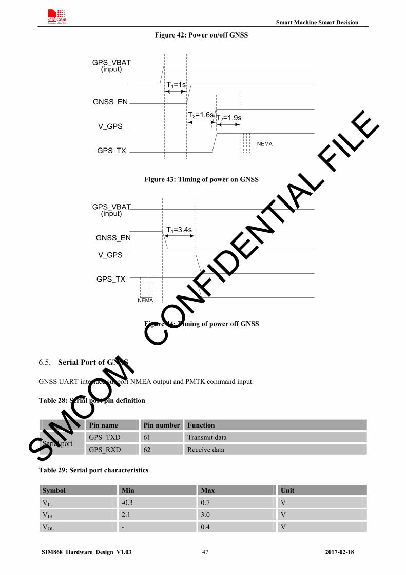
Smart Machine Smart Decision
SIM868_Hardware_Design_V1.03 47 2017-02-18
Figure 42: Power on/off GNSS
GPS_VBAT
GNSS_EN
GPS_TX
(input)
T1=1s
NEMA
V_GPST2=1.6s T2=1.9s
Figure 43: Timing of power on GNSS
GPS_VBAT
GNSS_EN
GPS_TX
(input)
T1=3.4s
NEMA
V_GPS
Figure 44: Timing of power off GNSS
6.5. Serial Port of GNSS
GNSS UART interface support NMEA output and PMTK command input.
Table 28: Serial port pin definition
Table 29: Serial port characteristics
Symbol Min Max Unit
VIL -0.3 0.7 V
VIH 2.1 3.0 V
VOL - 0.4 V
Pin name Pin number Function
Serial port GPS_TXD 61 Transmit data
GPS_RXD 62 Receive data SIMCOM C
ONFIDENTIA
L FILE

Smart Machine Smart Decision
SIM868_Hardware_Design_V1.03 48 2017-02-18
VOH 2.4 - V
6.6. Software Upgrade of GNSS
GNSS firmware can be upgraded through UART interface.
GPS_TXD
Module(GNSS)
GPS_RXD
GND
GNSS_EN
TXD
RXD
GND
Serial PortI/O Connector
2.8V10K
Figure 45: Connection for software upgrading and debugging for GNSS
If customer upgrades GSM and GNSS part in all-in-one mode, the GNSS UART should be connected to GSM UART2; GNSS_EN must be connected to GPIO1 of GSM part through 10K resistance. Thus customer could upgrade the module through UART1 or USB port of GSM.
GPS_TXD
SIM868 Module
GPS_RXDGNSS_EN
UART2_TXDUART2_RXD
R10R
GPIO1
R20R
R310K
Figure 46: Connection for software upgrading in all-in-one Mode
Note: GNSS_EN must be connected to GPIO1 of GSM part
6.7. 1PPS Output
The 1PPS pin outputs pulse-per-second signal for precise timing purposes after the position has been fixed. The 1PPS signal can be provided through designated output pin for many external applications. This pulse is not only limited to be active every second but also allowed to set the required duration, frequency, and active high/low by programming user-defined settings. Figure 47 is the typical application of the 1PPS function:
SIMCOM C
ONFIDENTIA
L FILE

Smart Machine Smart Decision
SIM868_Hardware_Design_V1.03 49 2017-02-18
Module
1PPS
GPS_VBAT
4.7K
47K
R
Figure 47: 1PPS Application circuit
6.8. Antenna Interface
Antenna interface of GNSS: The input impendence of the antenna should be 50Ω, and the VSWR should be less than 2. It is recommended that the GNSS antenna should be placed as far as possible to other antenna. The isolation of the antenna should be more than 30dB
Note:About RF design, please refer to document [15], [16] for more information.
6.8.1. Passive Antenna
Passive antenna contains only the radiating element, e.g.: the ceramic patch, the helix structure, and chip antennas. Sometimes it also contains a passive matching network to match the electrical connection to 50Ω impedance.
The most common antenna type for GPS/GLONASS application is the patch antenna. Patch antennas are flat, generally have a ceramic and metal body and are mounted on a metal base plate.
C101
MODULE
GPS_ANT
GND
C102
R101
Matching circuit
GNSS Passive
Antenna
(PIN68)
(PIN67)
BPF
Figure 48: GNSS passive antenna matching circuit
The components R101, C101 and C102 are used for antenna matching, the BPF is used for out of band noise signal suppression. The components’ value only can be got after the antenna tuning. Normally R101 is 0Ω, C101 and C102 are not mounted.
SIMCOM C
ONFIDENTIA
L FILE

Smart Machine Smart Decision
SIM868_Hardware_Design_V1.03 50 2017-02-18
6.8.2. Active Antenna
Active antenna has an integrated Low-Noise Amplifier (LNA). VCC_ANT is needed on customer’s application board for the active antenna power input, as shown in Figure 49.
C101
MODULE
GPS_ANT
GND C102
R101
Matching circuit
GNSS Active
AntennaL101 27nHR102 10Ω
VCC_ANT
(PIN68)
(PIN67)
BPF
Figure 49: GNSS active antenna matching circuit
The inductor L101 is used to prevent the RF signal from leaking into the VCC_ANT pass and route the bias supply to the active antenna, the recommended value of L101 is no less than 27nH. R102 can protect the whole circuit in case the active antenna is shorted to ground.
Table 30: Recommended BPF component
Package Type Supplier
1.10*0.90 SAFFB1G56KB0F0A Murata
6.9. Operation Modes of GNSS
GNSS supports operating modes like full on mode, stop mode, backup mode, periodic mode, AlwaysLocateTM mode and GLP mode. Full on mode: In this mode, the GNSS will enter full on mode after first power up. Power consumption will
vary depending on the amount of satellite acquisitions and number of satellites in track.
Table 31: Default configuration of GNSS (full on mode)
Item Configuration Comment
Baud rate Depend on firmware 9600/115200bps
GNSS GPS+GLONASS GPS/BEIDOU/GLONASS
Update rate 1Hz default 10Hz Max
SBAS Enable
AIC Enable
Note: The GNSS modes mentioned above are set by PMTK commands. The PMTK commands for multiple position chosen are illustrated as below:
$PMTK353,1,0,0,0,0*2A (GPS only) $PMTK353,0,0,0,0,1*2A (BEIDOU only)
SIMCOM C
ONFIDENTIA
L FILE
Smart Machine Smart Decision
SIM868_Hardware_Design_V1.03 51 2017-02-18
$PMTK353,0,1,0,0,0*2A (GLONASS only) $PMTK353,1,1,0,0,0*2B (GPS+GLONASS) $PMTK353,1,0,0,0,1*2B (GPS+BEIDOU)
Customer can refer to document [13] for more information. Stop mode: Stop mode means a low quiescent (590uA typ) power state and a PMTK command can be used
to enter. Any character input will exit from stop mode.
Note: Using the PMTK161 command to enter stop mode: "$PMTK161,0*28" Customer can refer to document [13] for more information. Backup mode: In this mode, the power source (such as battery) is connected to VRTC pin, which will help
to keep its internal RTC running when the GPS_VBAT is turned off. The VRTC power must be kept active all the time, the GNSS module will perform a quick start every power-on. Backup mode has lower power consumption than stop mode. The power consumption in this mode is about 8uA.
Periodic mode: In this mode, periodic control power on/off of GPS to reduce power consumption.
"$PMTK225,(Type),(Run time),(Sleep time),(Second run time),(Second sleep time)*15"
Note: Using the PMTK225 command to set periodic mode: Periodic backup mode: "$PMTK225,0*2B" "$PMTK223,1,25,180000,60000*38" "$PMTK225,1,3000,12000,18000,72000*15" Periodic stop mode: "$PMTK225,0*2B" "$PMTK223,1,25,180000,60000*38" "$PMTK225,2,3000,12000,18000,72000*15" Customer can refer to document [13] for more information.
AlwaysLocateTM mode: AlwaysLocateTM is an intelligent controller of GNSS periodic mode. Depending on
the environment and motion conditions, GNSS can adaptive adjust the on/off time to achieve balance of positioning accuracy and power consumption.
Note: Using the PMTK225 command to set AlwaysLocateTM mode. AlwaysLocateTM Stop mode: "$PMTK225,0" "$PMTK225,8" AlwaysLocateTM Backup mode: "$PMTK225,0" "$PMTK225,9"
Customer can refer to document [13] for more information.
GLP mode: The power consumption is lower in GLP (GNSS low power) mode. GNSS can be waked up when the host sends the command through the communication interface. GLP mode is to achieve 1Hz NMEA output and power saving, switch the Measurement Engine (DSP) and
SIMCOM C
ONFIDENTIA
L FILE
Smart Machine Smart Decision
SIM868_Hardware_Design_V1.03 52 2017-02-18
Positioning Engine (ARM) on/off. In GLP mode, the active time (on time) of Measurement Engine (DSP) and Positioning Engine (ARM) should be adjusted dynamically according to GNSS signal.
Note: Using the PMTK262 command to enable/disable GLP mode: "$PMTK262,3" Enable GLP mode; "$PMTK262,0" Disable GLP mode; Customer can refer to document [13] for more information.
6.10. A-GPS
A-GPS means assisted GPS, which is a system that can improve the startup performance and time-to-first-fix (TTFF) of a GNSS satellite-based positioning under certain conditions. GNSS part supports EPO file, EASY MODE and SBAS.
6.10.1. Easy Mode
Easy is the abbreviation of Embedded Assist System, it works as embedded firmware which accelerates TTFF by predicting satellite navigation messages from received ephemeris. No additional computing interval for Easy task. Easy is efficiently scheduled and computed in free time of every second after GNSS navigation solution. Easy function is conceptually designed to automatically engage for predicting after first receiving the broadcast ephemeris. After a while(generally tens of seconds), 3-day extensions will be completely generated then all Easy functions will be maintained at a standby condition. Easy assistance is going to be engaged when the GNSS requests in new TTFF condition or re-generates again with another new received ephemeris. Meanwhile, TTFF will be benefited by Easy assistance. Note: The modes mentioned above can be set by PMTK commands; customer can refer to document [13] for more information.
6.10.2. EPO
GNSS supports the EPO (Extended Prediction Orbit) data service. The EPO data service supports 7/14/30 days orbit prediction to customers. It needs to download aiding information from EPO server, which includes ephemeris, almanac, rough last position ,time, satellite status and an optional time synchronization signal. This function will reduce time of first fixing significantly and improving the acquisition sensitivity. Customer should update the EPO files from EPO server daily through the GSM part. Note: The modes mentioned above can be set by PMTK commands; customer can refer to document [13] for more information.
6.11. Fast-Fix
The Fast-Fix technology is based on the latest EPO data. Fast-Fix online provides extra time aiding from NITZ
SIMCOM C
ONFIDENTIA
L FILE
Smart Machine Smart Decision
SIM868_Hardware_Design_V1.03 53 2017-02-18
or NTP, which could reduce TTFF and acquisition sensitivity in cold start.
6.12. Multi-tone AIC
SIM868 module supports Multi-tone AIC (active interference canceller) to suppress the RF noise from GSM, Wi-Fi and so on. With the help of AIC function, The GNSS signal could be demodulated from the jammed signal, which can ensure better navigation quality. AIC function is enabled by default. Enabling AIC function will increase extra current consumption Note: Using the PMTK286 command to enable/disable AIC function:
Enable AIC function: $PMTK286,1*23 Disable AIC function: $PMTK286,0*22
6.13. SBAS
SBAS is the abbreviation of Satellite Based Augmentation System. The SBAS concept is based on the transmission of differential corrections and integrity messages for navigation satellites that are within sight of a network of reference stations deployed across an entire continent. SBAS messages are broadcast via geostationary satellites that are able to cover vast areas. Several countries have implemented their own satellite-based augmentation system. Europe has the European Geostationary Navigation Overlay Service (EGNOS) which covers Western Europe and beyond. The USA has its Wide Area Augmentation System (WAAS). Japan is covered by its Multi-functional Satellite Augmentation System (MSAS). India has launched its own SBAS program named GPS and GEO Augmented Navigation (GAGAN) to cover the Indian subcontinent.
SIMCOM C
ONFIDENTIA
L FILE

Smart Machine Smart Decision
SIM868_Hardware_Design_V1.03 54 2017-02-18
7. PCB Layout This section provides some guidelines on PCB layout, in order to eliminate interference or noise.
7.1. Pin Assignment
Before PCB layout, we should learn about pin assignment in order to get reasonable layout with so many external components. Figure 50 is the overview of pin assignment of the module.
MCCK
UART1_DTR
USB_DP
GPS_VBATVBATADC
UART1_RXD
PWRKEY
UART1_CTS
UART1_TXD
UART1_RTS
SCL SDA
UART1_DCD
NETLIGHT
SIM1_RSTSIM1_CLKSIM1_DET SIM1_DATA BT_ANT
SIM2_CLKSIM2_DET SIM2_DATA SIM2_RST SIM2_VDD
UART2_TXD
SPK1P
VRTC
MICP
MICN USB_VBUS
USB_DM
GSM_ANT
STATUS
SIM1_VDD
MCCA3
GND
UART2_RXD
GND
GPS_RXD
GNSS_EN
1PPS
GPIO2
GPS_TXD
13
SPK1N
UART1_RI
GPS_ANT
14 15 16 2117 18 19 20
22
23
24
25
26
27
28
29
30
31
32
33
37 36 35 34
1
42 41 40 39 38
5
4
2
3
6
11
10
9
8
7
51125352 5554 5756
58
62
61
60
59
67 66 65 64 63
46
45
44
43
49
48
47
50
VDD_EXT
GND
GND
GND
GND
GND
GND
GPIO1
GND
GND
GND
GND
UART1_DTR
RF_SYNC
GND
GND
SPK2P
68
MCCM0
MCCA1
SPK2N
MCCA2
MCCA0
GND GNDGND
GNDGNDGND
GNDGNDGND
7669 75
70 77 74
71 72 73
Figure 50: PIN assignment
SIMCOM C
ONFIDENTIA
L FILE

Smart Machine Smart Decision
SIM868_Hardware_Design_V1.03 55 2017-02-18
7.2. Principle of PCB Layout
7.2.1. Antenna Interface
Antenna interface used for RF conducting test such as coaxial cable pad, RF connector should be placed close to RF_IN pad.
RF trace should be as short and direct as possible. Keep the impedance of RF traces as 50Ω; Avoid any other signal crossing or parallel directly under the RF trace.
7.2.2. Power Supply
VBAT and GND are very important in layout. The VBAT trace should be as short and wide as possible. Zener diode and capacitor should be placed close to VBAT pin. The trace of pin 36 and pin37 to main GND should be as short and wide as possible.
7.2.3. SIM Card Interface
Ensure SIM card holder is far away from antenna or RF cable to avoid high power interference of GSM transmitter.
Put SIM card holder near the module. Add ESD component to protect SIM_CLK, SIM_DATA, SIM_RST and SIM_VDD signals. All the signals should be far away from power and high-speed-frequency signal. The length of signals should be less than 100mm.
7.2.4. Audio Interface
The signal trace of audio should be far away from antenna The signal trace of audio should not parallel to VBAT The audio trace are surrounded with GND
SIMCOM C
ONFIDENTIA
L FILE
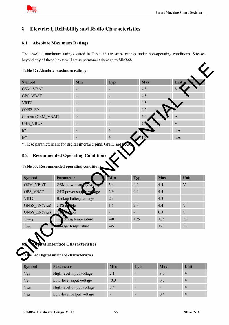
Smart Machine Smart Decision
SIM868_Hardware_Design_V1.03 56 2017-02-18
8. Electrical, Reliability and Radio Characteristics
8.1. Absolute Maximum Ratings
The absolute maximum ratings stated in Table 32 are stress ratings under non-operating conditions. Stresses beyond any of these limits will cause permanent damage to SIM868.
Table 32: Absolute maximum ratings
Symbol Min Typ Max Unit
GSM_VBAT - - 4.5 V
GPS_VBAT - - 4.5
VRTC - - 4.5
GNSS_EN - - 4.5
Current (GSM_VBAT) 0 - 2.0 A
USB_VBUS - - 7 V
II* - 4 16 mA
IO* - 4 16 mA
*These parameters are for digital interface pins, GPIO, and UART.
8.2. Recommended Operating Conditions
Table 33: Recommended operating conditions
Symbol Parameter Min Typ Max Unit
GSM_VBAT GSM power supply voltage 3.4 4.0 4.4 V
GPS_VBAT GPS power supply voltage 2.9 4.0 4.4
VRTC Backup battery voltage 2.3 4.3
GNSS_EN(VOH) GPS enable 1.5 2.8 4.4 V
GNSS_EN(VOL) GPS disable - - 0.3 V
TOPER Operating temperature -40 +25 +85
TSTG Storage temperature -45 +90
8.3. Digital Interface Characteristics
Table 34: Digital interface characteristics
Symbol Parameter Min Typ Max Unit
VIH High-level input voltage 2.1 - 3.0 V
VIL Low-level input voltage -0.3 - 0.7 V
VOH High-level output voltage 2.4 - - V
VOL Low-level output voltage - - 0.4 V
SIMCOM C
ONFIDENTIA
L FILE
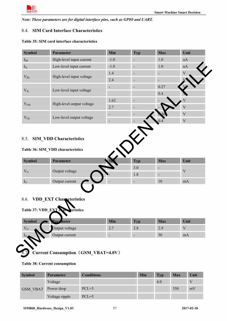
Smart Machine Smart Decision
SIM868_Hardware_Design_V1.03 57 2017-02-18
Note: These parameters are for digital interface pins, such as GPIO and UART.
8.4. SIM Card Interface Characteristics
Table 35: SIM card interface characteristics
Symbol Parameter Min Typ Max Unit
IIH High-level input current -1.0 - 1.0 uA
IIL Low-level input current -1.0 - 1.0 uA
VIH High-level input voltage 1.4 - - V
2.4 - - V
VIL Low-level input voltage - - 0.27 V
0.4 V
VOH High-level output voltage 1.62 - - V
2.7 - - V
VOL Low-level output voltage - - 0.36 V
- - 0.4 V
8.5. SIM_VDD Characteristics
Table 36: SIM_VDD characteristics
Symbol Parameter Min Typ Max Unit
VO Output voltage - 3.0 -
V - 1.8 -
IO Output current - - 10 mA
8.6. VDD_EXT Characteristics
Table 37: VDD_EXT characteristics
Symbol Parameter Min Typ Max Unit
VO Output voltage 2.7 2.8 2.9 V
IO Output current - - 50 mA
8.7. Current Consumption(GSM_VBAT=4.0V)
Table 38: Current consumption
Symbol Parameter Conditions Min Typ Max Unit
GSM_VBAT
Voltage 4.0 V
Power drop PCL=5 350 mV
Voltage ripple PCL=5
SIMCOM C
ONFIDENTIA
L FILE
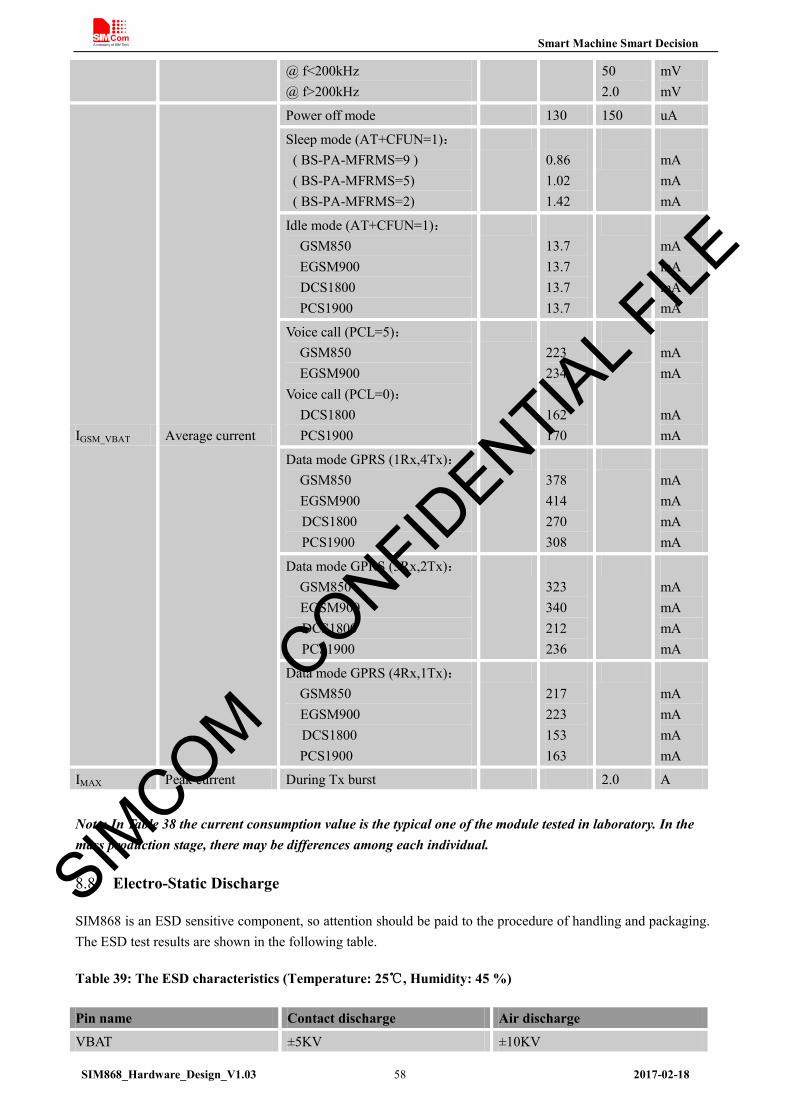
Smart Machine Smart Decision
SIM868_Hardware_Design_V1.03 58 2017-02-18
@ f<200kHz @ f>200kHz
50 2.0
mV mV
IGSM_VBAT Average current
Power off mode 130 150 uA
Sleep mode (AT+CFUN=1): ( BS-PA-MFRMS=9 ) ( BS-PA-MFRMS=5) ( BS-PA-MFRMS=2)
0.86 1.02 1.42
mA mA mA
Idle mode (AT+CFUN=1): GSM850 EGSM900 DCS1800 PCS1900
13.7 13.7 13.7 13.7
mA mA mA mA
Voice call (PCL=5): GSM850 EGSM900
Voice call (PCL=0): DCS1800 PCS1900
223 234 162 170
mA mA mA mA
Data mode GPRS (1Rx,4Tx): GSM850 EGSM900 DCS1800 PCS1900
378 414 270 308
mA mA mA mA
Data mode GPRS (3Rx,2Tx): GSM850 EGSM900 DCS1800 PCS1900
323 340 212 236
mA mA mA mA
Data mode GPRS (4Rx,1Tx): GSM850 EGSM900 DCS1800 PCS1900
217 223 153 163
mA mA mA mA
IMAX Peak current During Tx burst 2.0 A
Note: In Table 38 the current consumption value is the typical one of the module tested in laboratory. In the mass production stage, there may be differences among each individual.
8.8. Electro-Static Discharge
SIM868 is an ESD sensitive component, so attention should be paid to the procedure of handling and packaging. The ESD test results are shown in the following table.
Table 39: The ESD characteristics (Temperature: 25, Humidity: 45 %)
Pin name Contact discharge Air discharge
VBAT ±5KV ±10KV
SIMCOM C
ONFIDENTIA
L FILE

Smart Machine Smart Decision
SIM868_Hardware_Design_V1.03 59 2017-02-18
GND ±5KV ±10KV
UART1_TXD /UART1_RXD ±4KV ±8KV
Antenna port ±5KV ±10KV
SPKP/SPKN/MICP/MICN ±4KV ±8KV
PWRKEY ±4KV ±8KV
8.9. Radio Characteristics
8.9.1. Module RF Output Power
The Table 40 shows the module conducted output power, it follows the 3GPP TS 05.05 technical specification requirement.
Table 40: GSM850 and EGSM900 conducted RF output power
GSM850, EGSM900
PCL Nominal output power (dBm) Tolerance (dB) for conditions
Normal Extreme
5 33 ±2 ±2.5
6 31 ±3 ±4
7 29 ±3 ±4
8 27 ±3 ±4
9 25 ±3 ±4
10 23 ±3 ±4
11 21 ±3 ±4
12 19 ±3 ±4
13 17 ±3 ±4
14 15 ±3 ±4
15 13 ±3 ±4
16 11 ±5 ±6
17 9 ±5 ±6
18 7 ±5 ±6
19-31 5 ±5 ±6
Table 41: DCS1800 and PCS1900 conducted RF output power
DCS1800,PCS1900
PCL Nominal output power (dBm) Tolerance (dB) for conditions
Normal Extreme
0 30 ±2 ±2.5
1 28 ±3 ±4
2 26 ±3 ±4
3 24 ±3 ±4
SIMCOM C
ONFIDENTIA
L FILE

Smart Machine Smart Decision
SIM868_Hardware_Design_V1.03 60 2017-02-18
4 22 ±3 ±4
5 20 ±3 ±4
6 18 ±3 ±4
7 16 ±3 ±4
8 14 ±3 ±4
9 12 ±4 ±5
10 10 ±4 ±5
11 8 ±4 ±5
12 6 ±4 ±5
13 4 ±4 ±5
14 2 ±5 ±6
15 0 ±5 ±6
For the module’s output power, the following should be noted: At GSM900 and GSM850 band, the module is a class 4 device, so the module’s output power should not exceed 33dBm, and at the maximum power level, the output power tolerance should not exceed +/-2dB under normal condition and +/-2.5dB under extreme condition. At DCS1800 and PCS1900 band, the module is a class 1 device, so the module’s output power should not exceed 30dBm, and at the maximum power level, the output power tolerance should not exceed +/-2dB under normal condition and +/-2.5dB under extreme condition.
8.9.2. Module RF Receive Sensitivity
Table 42 shows the module’s conducted receiving sensitivity; it is tested under static condition.
Table 42: Conducted RF receive sensitivity
Frequency Receive sensitivity(Typical) Receive sensitivity(Max)
GSM850,EGSM900 < -109dBm < -107dBm
DCS1800,PCS1900 < -109dBm < -107dBm
8.9.3. Module Operating Frequencies
The Table 43 shows the module’s operating frequency range; it follows the 3GPP TS 05.05 technical specification requirement.
Table 43: Operating frequencies
Frequency Receive Transmit
GSM850 869 ~ 894MHz 824 ~ 849MHz
EGSM900 925 ~ 960MHz 880 ~ 915MHz
DCS1800 1805 ~ 1880MHz 1710 ~ 1785MHz
PCS1900 1930 ~ 1990MHz 1850 ~ 1910MHz
SIMCOM C
ONFIDENTIA
L FILE
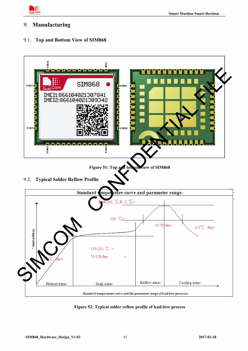
Smart Machine Smart Decision
SIM868_Hardware_Design_V1.03 61 2017-02-18
9. Manufacturing
9.1. Top and Bottom View of SIM868
Figure 51: Top and bottom view of SIM868
9.2. Typical Solder Reflow Profile
Figure 52: Typical solder reflow profile of lead-free process
SIMCOM C
ONFIDENTIA
L FILE

Smart Machine Smart Decision
SIM868_Hardware_Design_V1.03 62 2017-02-18
9.3. The Moisture Sensitivity Level
The moisture sensitivity level of SIM868 module is 3. The modules should be mounted within 168 hours after unpacking in the environmental conditions of temperature <30 and relative humidity of <60% (RH). It is necessary to bake the module if the above conditions are not met:
Table 44: Moisture sensitivity level and floor life
Moisture Sensitivity Level (MSL)
Floor Life (out of bag) at factory ambient≤30°C/60% RH or as stated
1 Unlimited at ≦30/85% RH
2 1 year
2a 4 weeks
3 168 hours
4 72 hours
5 48 hours
5a 24 hours
6 Mandatory bake before use. After bake, it must be reflowed within the time limit specified on the label.
NOTES: 1. If the vacuum package is not open for 3 months or longer than the packing date, baking is also recommended before re-flow soldering. 2. For product handling, storage, processing, IPC / JEDEC J-STD-033 must be followed.
9.4. Baking Requirements
SIM868 modules are vacuum packaged, and guaranteed for 6 months storage without opening or leakage under the following conditions: the environment temperature is lower than 40, and the air humidity is less than 90%.
If the condition meets one of the following ones shown below, the modules should be baked sufficiently before re-flow soldering, and the baking condition is shown in table below; otherwise the module will be at the risk of permanent damage during re-flow soldering. If the vacuum package is broken or leakage;
If the vacuum package is opened after 6 months since it’s been packed;
If the vacuum package is opened within 6 months but out of its Floor Life at factory ambient≦30/60%RH or as stated.
Table 45: Baking requirements
Baking temperature Moisture Time
40±5 <5% 192 hours
120±5 <5% 4 hours
Note: Care should be taken if that plastic tray is not heat-resistant, the modules should be taken out for preheating, and otherwise the tray may be damaged by high-temperature heating.
SIMCOM C
ONFIDENTIA
L FILE

Smart Machine Smart Decision
SIM868_Hardware_Design_V1.03 63 2017-02-18
10. Appendix
10.1. Related Documents
Table 46: Related documents
SN Document name Remark
[1] SIM800_Series_AT_Command_Manual
[2] SIM800 Series UART Port Application Note_V1.01.doc
[3] SIM800 Series_TCPIP_Application Note_V1.02
[4] ITU-T Draft new recommendation V.25ter:
Serial asynchronous automatic dialing and control
[5] GSM 07.07: Digital cellular telecommunications (Phase 2+); AT command set for GSM Mobile Equipment (ME)
[6] GSM 07.10: Support GSM 07.10 multiplexing protocol
[7] GSM 07.05:
Digital cellular telecommunications (Phase 2+); Use of Data Terminal Equipment – Data Circuit terminating Equipment (DTE – DCE) interface for Short Message Service (SMS) and Cell Broadcast Service (CBS)
[8] GSM 11.14:
Digital cellular telecommunications system (Phase 2+); Specification of the SIM Application Toolkit for the Subscriber Identity Module – Mobile Equipment (SIM – ME) interface
[9] GSM 11.11: Digital cellular telecommunications system (Phase 2+); Specification of the Subscriber Identity Module – Mobile Equipment (SIM – ME) interface
[10] GSM 03.38: Digital cellular telecommunications system (Phase 2+); Alphabets and language-specific information
[11] GSM 11.10 Digital cellular telecommunications system (Phase 2); Mobile Station (MS) conformance specification; Part 1: Conformance specification
[12] AN_Serial Port AN_Serial Port
[13] SIM868_NMEA Message Specification_V1.00
[14] EPO-II_Format_Protocol_Customer EPO-II_Format and Protocol
[15] SIM868_RF_Design_Application Note
[16] AN_SMT Module_RF_Reference Design_Guide
SIMCOM C
ONFIDENTIA
L FILE

Smart Machine Smart Decision
SIM868_Hardware_Design_V1.03 64 2017-02-18
10.2. Terms and Abbreviations
Table 47: Terms and abbreviations
Abbreviation Description
ADC Analog-to-Digital Converter
AMR Adaptive Multi-Rate
CS Coding Scheme
CTS Clear to Send
DTE Data Terminal Equipment (typically computer, terminal, printer)
DTR Data Terminal Ready
DTX Discontinuous Transmission
EFR Enhanced Full Rate
EGSM Enhanced GSM
ESD Electrostatic Discharge
ETS European Telecommunication Standard
FR Full Rate
GPRS General Packet Radio Service
GSM Global Standard for Mobile Communications
HR Half Rate
MO Mobile Originated
MS Mobile Station (GSM part), also referred to as TE
MT Mobile Terminated
PAP Password Authentication Protocol
PBCCH Packet Broadcast Control Channel
PCB Printed Circuit Board
PCL Power Control Level
PCS Personal Communication System, also referred to as GSM 1900
PDU Protocol Data Unit
PPP Point-to-point protocol
RF Radio Frequency
RMS Root Mean Square (value)
RX Receive Direction
SIM Subscriber Identification Module
SMS Short Message Service
TE Terminal Equipment, also referred to as DTE
TX Transmit Direction
SINAD Signal to Noise and Distortion Ratio
UART Universal Asynchronous Receiver & Transmitter
URC Unsolicited Result Code
USSD Unstructured Supplementary Service Data
SIMCOM C
ONFIDENTIA
L FILE
Smart Machine Smart Decision
SIM868_Hardware_Design_V1.03 65 2017-02-18
A-GPS Assisted Global Positioning System
CMOS Complementary Metal Oxide Semiconductor
CEP Circular Error Probable
GLP GNSS Low Power
DGPS Difference Global Positioning System
EEPROM Electrically Erasable Programmable Read Only Memory
EPO Extended Prediction Orbit
ESD Electrostatic Sensitive Devices
EASY Embedded Assist System
EGNOS European Geostationary Navigation Overlay Service
GPS Global Positioning System
GAGAN The GPS Aided Geo Augmented Navigation
kbps Kilo bits per second
MSL moisture sensitive level
MSAS Multi-Functional Satellite Augmentation System
NMEA National Marine Electronics Association
PRN Pseudo Random Noise Code
QZSS Quasi-Zenith Satellites System
SBAS Satellite Based Augmentation Systems
WAAS Wide Area Augmentation System
Phonebook abbreviations
FD SIM fix dialing phonebook
LD SIM last dialing phonebook (list of numbers most recently dialed)
MC Mobile Equipment list of unanswered MT calls (missed calls)
ON SIM (or ME) own numbers (MSISDNs) list
RC Mobile Equipment list of received calls
SM SIM phonebook
NC Not connect
SIMCOM C
ONFIDENTIA
L FILE

Smart Machine Smart Decision
SIM868_Hardware_Design_V1.03 66 2017-02-18
10.3. Safety Caution
Table 48: Safety caution
Marks Requirements
When in a hospital or other health care facility, observe the restrictions about the use of mobiles. Switch the cellular terminal or mobile off, medical equipment may be sensitive to not operate normally for RF energy interference.
Switch off the cellular terminal or mobile before boarding an aircraft. Make sure it is switched off. The operation of wireless appliances in an aircraft is forbidden to prevent interferes with communication systems. Forget to think much of these instructions may lead to the flight safety or offend against local legal action, or both.
Do not operate the cellular terminal or mobile in the presence of flammable gases or fumes. Switch off the cellular terminal when you are near petrol stations, fuel depots, chemical plants or where blasting operations are in progress. Operation of any electrical equipment in potentially explosive atmospheres can constitute a safety hazard.
Your cellular terminal or mobile receives and transmits radio frequency energy while switched on. RF interferes can occur if it is used close to TV sets, radios, computers or other electric equipment.
Road safety comes first! Do not use a hand-held cellular terminal or mobile when driving a vehicle, unless it is securely mounted in a holder for hands free operation. Before making a call with a hand-held terminal or mobile, park the vehicle.
GSM cellular terminals or mobiles operate over radio frequency signals and cellular networks and cannot be guaranteed to connect in all conditions, for example no mobile fee or a invalid SIM card. While you are in this condition and need emergent help, please remember using emergency calls. In order to make or receive calls, the cellular terminal or mobile must be switched on and in a service area with adequate cellular signal strength. Some networks do not allow for emergency call if certain network services or phone features are in use (e.g. lock functions, fixed dialing etc.). You may have to deactivate those features before you can make an emergency call. Also, some networks require that a valid SIM card be properly inserted in the cellular terminal or mobile.
SIMCOM C
ONFIDENTIA
L FILE

Smart Machine Smart Decision
SIM868_Hardware_Design_V1.03 67 2017-02-18
Contact us: Shanghai SIMCom Wireless Solutions Co.,Ltd. Address: Building A, SIM Technology Building, No. 633, Jinzhong Road, Shanghai, P. R. China 200335 Tel: +86 21 3252 3300 Fax: +86 21 3252 3020 URL: www.simcomm2m.com
SIMCOM C
ONFIDENTIA
L FILE