
FIGARO FG-030 CO2 SENSOR MANUAL &...
40
Revised 11/17 1 Page Basic Information and Specifications Features.....................................................................................................2 Applications.............................................................................................2 Basic Principle and Structure..................................................................2 Operating Conditions and Specifications...........................................2 Absolute Maximum Ratings..................................................................2 Dimensions.............................................................................................3 Functions ..................................................................................... 3 Pin Configuration/Functions...................................................................3 Installation and Soldering Conditions.........................................................4 Reliability Long Term Stability ........................................................................ 5 Corrosion Test ........................................................................ 5 Dust Test................................................................................................5 Temperature Cycle Test.................................................................. 5 High/Low Temperature Test............................................................5 Communication UART Communication.....................................................................6 I2C Communication.................................................................. 8 Housing Design...............................................................................................10 Packaging..............................................................................................11 Maintenance ................................................................................... 11 Handling Precautions ................................................................... 11 Frequently Asked Questions ............................................................ 12 Part 2: Communication Specifications ..... ......................................... 13 IMPORTANT NOTE: OPERATING CONDITIONS IN WHICH FIGARO SENSORS ARE USED WILL VARY WITH EACH CUSTOMER’S SPECIFIC APPLICATIONS. FIGARO STRONGLY RECOMMENDS CONSULTING OUR TECHNICAL STAFF BEFORE DEPLOYING FIGARO SENSORS IN YOUR APPLICATION AND, IN PARTICULAR, WHEN CUSTOMER’S TARGET GASES ARE NOT LISTED HEREIN. FIGARO CANNOT ASSUME ANY RESPONSIBILITY FOR ANY USE OF ITS SENSORS IN A PRODUCT OR APPLICATION FOR WHICH THE SENSOR HAS NOT BEEN SPECIFICALLY TESTED BY FIGARO. The FG-030 CO2 module uses a nondispersive infrared (NDIR) sensor principle and compact optics to achieve excellent performance characteristics, including high accuracy and low power con- sumption. Two detector elements inside the module make absolute measurement possible. Every module is individually calibrated and is provided with both a UART and I2C digital interface. The FG-030 module is designed for simple integration into a user's products. It can be used in a wide range of applications such as ventilation controls for the improvement of energy savings and to assure a good indoor climate. F IGARO FG-030 CO2 SENSOR MANUAL & COMMUNICATION SPECIFICATIONS
Transcript of FIGARO FG-030 CO2 SENSOR MANUAL &...

Revised 11/17 1
PageBasic Information and Specifications
Features.....................................................................................................2 Applications.............................................................................................2
Basic Principle and Structure..................................................................2Operating Conditions and Specifications...........................................2Absolute Maximum Ratings..................................................................2
Dimensions.............................................................................................3 Functions.....................................................................................3
Pin Configuration/Functions...................................................................3Installation and Soldering Conditions.........................................................4
ReliabilityLong Term Stability........................................................................5Corrosion Test........................................................................5Dust Test................................................................................................5Temperature Cycle Test..................................................................5High/Low Temperature Test............................................................5
CommunicationUART Communication.....................................................................6I2C Communication..................................................................8
Housing Design...............................................................................................10
Packaging..............................................................................................11
Maintenance...................................................................................11
Handling Precautions...................................................................11
Frequently Asked Questions............................................................12Part 2: Communication Specifications..... .........................................13
IMPORTANT NOTE: OPERATING CONDITIONS IN WHICH FIGARO SENSORS ARE USED WILL VARY WITH EACH CUSTOMER’S SPECIFIC APPLICATIONS. FIGARO STRONGLY RECOMMENDS CONSULTING OUR TECHNICAL STAFF BEFORE DEPLOYING FIGARO SENSORS IN YOUR APPLICATION AND, IN PARTICULAR, WHEN CUSTOMER’S TARGET GASES ARE NOT LISTED HEREIN. FIGARO CANNOT ASSUME ANY RESPONSIBILITY FOR ANY USE OF ITS SENSORS IN A PRODUCT OR APPLICATION FOR WHICH THE SENSOR HAS NOT BEEN SPECIFICALLY TESTED BY FIGARO.
The FG-030 CO2 module uses a nondispersive infrared (NDIR) sensor principle and compact optics to achieve excellent performance characteristics, including high accuracy and low power con-sumption. Two detector elements inside the module make absolute measurement possible. Every module is individually calibrated and is provided with both a UART and I2C digital interface. The FG-030 module is designed for simple integration into a user's products. It can be used in a wide range of applications such as ventilation controls for the improvement of energy savings and to assure a good indoor climate.
FIGARO FG-030 CO2 SENSOR MANUAL & COMMUNICATION SPECIFICATIONS

Revised 11/17 2
1. Basic Information and Specifications
1-1 Features* Small size* Low power* High accuracy* Absolute measurement via dual sensors
1-2 Applications:* Indoor air quality control* Fresh air ventilators* Air conditioners* Automatic fans and window openers
1-3 Basic principle and structureFig. 1 shows the basic principle of measuringabsolute values. Fig. 2 shows the basic structure ofthe module's optics.
This sensor is a single light source, dual wavelength system. The sensor employs two detectors with different optical filters in front of each detector. One detector measures the intensity of infrared light passing through the optical filter, transmitting only the infrared wavelength region absorbed by CO2 (CO2 absorption wavelength). The other detector measures the intensity of infrared light passing through the optical filter, transmitting only an infrared wavelength (3.8μm) not absorbed by CO2 (i.e. a reference wavelength), and is thus unaffected by the constant presence of CO2.
Measuring absolute values of CO2 concentration by FG-030 is achieved by the module's microprocessor calculating CO2 concentration from the difference between light intensity transmitted at the CO2 absorption wavelength and at the reference wavelength.
The single light source, dual wavelength system employed by the FG-030 measures light intensities at two different wavelengths after separation by two optical filters, thus compensating drift due to accumulated dust and contamination. This ensures long term stability, minimum maintenance, and cost-effectiveness.
1-4 Operating conditions & specifications(refer to Table 1)
1-5 Absolute maximum ratings (refer to Table 2)Products using FG-030 should be designed so that these maximum ratings are never exceeded.
Fig. 1 - Basic principle for measuring absolute values
Infrared spectrum CO2
1.0
03 3.5 3.8 4 4.3 4.5 5 5.5
0.8
0.6
0.4
0.2
Reference
Differenceis measured
wavelength
CO2 absorptionwavelength
Wavelength [µm]
Tran
smitt
ance
CO2 gas
Detectorelement
Optical filter
(for referencewavelength)
Optical filter
(for CO2 absorptionwavelength)
Lightsource
Infraredlight
Fig. 2 - Basic structure of FG-030 optics
Product name Carbon dioxide (CO2) sensor module
Model No. FG-030
Detection range 300~5,000ppm CO2
Operating principle Non-dispersive infrared (NDIR)
Power supply 4.75~5.25V DC
Current consumption 60mA peak, 10mA avg.
Accuracy (Note 1) ±(50ppm+3% of reading)in the range of 300~5,000ppm CO2
Pressure dependency approx 1% of reading / kPa
Response time (T90) 2 min. (diffusion)
Operating conditions 0~50˚C/0~85%RH (no condensation)
Storage conditions -30~70˚C/0~85%RH (no condensation)
Communication port UART/ I2C (gas conc. output 0~10,000ppm)
Measurement interval 2 sec.
PWM output (1kHz) 0~100% duty cycle for 0~5,000ppm,CMOS output
Alarm output CMOS output:High>1,000ppm Low<900ppm
Dimensions 32 x 17 x 7.5 (mm)
Weight approx. 3g
Table 1 - Specifications of FG-030Note 1: Represents accuracy at the time of factory test. For long term accuracy, please refer to Fig. 5 - Long term stability of FG-030.

Revised 11/17 3
1-6 Dimensions (Fig. 3)
1-7 FunctionsFG-030 has the following 4 major functions:
1-7-1 CO2 concentration outputFG-030 has two CO2 concentration outputs. One is PWM output (please refer to Sec. 1-8-3 - Pin No.4 ), theother is digital output through the communicationport (please refer to Sec. 3 - Communication).
1-7-2 Alarm signal outputFG-030 has an alarm signal output. Please refer toSec 1-8-3. Pin No.3 (Alarm) for further informationabout this signal.
1-7-3 Calibration functionFG-030 has two calibration functions. One is airadjustment, the other is zero adjustment. With airadjustment, CO2 concentration output is set at400ppm, assuming the sensor is exposed to 400ppmCO2 (normal CO2 levels in clean air are approx. 400ppm).With zero adjustment, CO2 concentration output isset at 0ppm, assuming the sensor is exposed to 0ppm CO2. For further details, please refer to Sec 1-8-6. PinNo.7 (CAL).
1-7-4 Atmospheric pressure and altitude compensationThe factory default setting of FG-030 for atmo-spheric pressure and altitude is fixed at 1013.25 hPaand 0m. Since FG-030 has pressure and altitudedependency, compensation for atmospheric pressure and altitude is needed to obtain high accuracy under different pressures/altitudes. To compensate, please refer to the document FG-030 CommunicationSpecifications.
1-8 Pin configurations and functions (Table 3)
1-8-1 Pin No.1 (VDD)Since a voltage regulator is included in the sensor,input voltage variation within the range of 4.75~5.25V does not affect output voltage of the sensor.
1-8-2 Pin No.3 (ALARM)The factory settings of the alarm threshold are1000ppm for alarm trigger and 900ppm for alarmreset. The thresholds are user-changable. Pleaserefer to the document FG-030 CommunicationSpecifications.
Item Min. Max. u/m
Ambient temperature -40 85 ˚C
Input voltage -0.3 5.5 V
Maximum input voltage(MSEL in, CAD in, CAL in,
Rx/SCL)-0.3 VDD+0.2
and 5.5 V
Maximum output current(Alarm, PWM, Busy, Tx/SDA) - 50 mA
Table 2 - Absolute maximum ratings for FG-030
6.8
2.15
2.54
3.9
1.6 1
1
2.15
1712.7
29.732
5
6
1 11
5
6
1 11
26
Non-woven fabricHole diameter
VDDGND
ALARMPWM
CAD0
NCRX/SCLTX/SDABUSYCALMSEL
unit: mm
Pin connection
Top view
Side view
ø0.9
Fig. 3 - Dimensions of FG-030
Pin No Name Description1 VDD Input voltage
2 GND Common ground
3 ALARM Alarm output
4 PWM PWM output
5 CAD0 I2C slave address selection input(internal pull up)
6 MSEL Communication mode signal inputI2C/UART (internal pull up)
7 CAL Air/zero adjustment input(internal pull up)
8 BUSY BUSY signal output
9 Tx/SDA UART Tx output/ I2C SDA input/output
10 Rx/SCL UART Rx input/ I2C SCL input
11 NC not connected
Table 3 - Pin configurations and functions of FG-030

Revised 11/17 4
1-8-3 Pin No.4 (PWM)A pulse of 1kHz that corresponds to 0~5,000ppm CO2is output from Pin No.4. A PWM signal can be easilyconverted to analog voltage. Please refer to Fig.4 foran example circuit.
1-8-4 Pin No.5 (CAD0)This port is for the selection of the least significant bit of the I2C slave address. By assigning High or Low to each slave, a maximum of 2 units of FG-030 can beconnected to one I2C bus. Since this pin is internallypulled up, if this port is not connected, High is input.
1-8-5 Pin No.6 (MSEL)For I2C communication, this pin should be connected to Low. The MSEL pin is internally pulled up. If theMSEL pin is not connected, the UART interface isused.
1-8-6 Pin No.7 (CAL)When Low voltage is applied to this port, calibration mode is activated. During normal operation (i.e.when calibration is not being performed), pleaseconnect to High or do not connect (open). (This pinis internally pulled up.)
When this pin is connected to Low for 4~10 sec., air adjustment is carried out assuming 400ppm exposure to the sensor.
When connected to Low for 12 sec. or longer, zero adjustment is carried out assuming 0ppm exposure to the sensor.
1-8-7 Pin No.8 (BUSY)The sensor may not communicate for a short period(about 0.3 sec.) due to the internal processing.During the BUSY state, High signal is output. Formore detail, please refer to the document FG-030Communication Specifications.
1-8-8 Pin No. 9 (Tx/SDA)This port works as a Tx port for UART communication and as a SDA (data) port for I2C communication.
1-8-9 Pin No. 10 (Rx/SCL)This port works as an Rx port for UART communication and as a SCL (clock) port for I2C communication.
1-9 Installation and soldering conditionsFG-030 can be mounted on a mother printed circuitboard by soldering the 0.9mmφ terminal holes of the sensor to pin strips of a 2.54mm pitch.
R1
C1
1µF
R2OUT(0-5V)
0V100
100kPWM(Pin 4)
Fig. 4 - PWM signal conversion circuit
0
1000
2000
3000
4000
5000
6000
0 100 200 300 400 500
Display Reading (ppm)
Time (days)
0ppm
400ppm
1000ppm
2000ppm
3000ppm
5000ppm
N=4
Fig. 5 - Long term stability of FG-030
0
1000
2000
3000
4000
5000
6000
0 5 10 15 20 25 30
0ppm400ppm1000ppm2000ppm3000ppm5000ppm
Display Reading (ppm)
Time (days)
Fig. 6-1 - Durability of FG-030 against H2S
-1000
0
1000
2000
3000
4000
5000
6000
0 5 10 15 20 25 30
0ppm400ppm1000ppm2000ppm3000ppm5000ppm
Display Reading (ppm)
Time (days)
Fig. 6-2 - Durability of FG-030 against SO2

Revised 11/17 5
2. Reliability2-1 Long term stabilityFig. 5 shows the long term stability of the sensor. The Y-axis shows CO2 concentration output at variousconcentrations of CO2. The CO2 concentration output is stable during the test period.
2-2 Corrosion testThe influence of corrosive gases on the sensor wasevaluated. Test samples were stored at 40˚C/82%RH. Under this condition, two different tests were carried out:
1) exposure to 3ppm H2S for 28 days2) exposure to 10ppm SO2 for 28 days
After gas exposure was concluded, CO2 concentration output was measured.
Fig. 6-1 and Fig. 6-2 show the durability test results for H2S and SO2 respectively. The test results demonstrate that there is no significant influence on the sensor from this corrosive gas exposure test.
2-3 Dust testDurability against dust exposure was tested. Fivedifferent types of dust as specified by JIS Z 8901were dropped onto the sensor continuously for 15minutes under conditions of 22˚C/41%RH. Fig. 7shows CO2 concentration output before and afterthe dust test. This demonstrates that there is nosignificant influence from this dust exposure test onsensor performance.
2-4 Temperature cycle testDurability to temperature cycling was tested. Testsamples were exposed to 500 cycles of -30˚C/30minutes and 70˚C/30 minutes. The test results shown in Fig. 8 demonstrate that there is no significantinfluence on the sensor from the extreme conditionsof this temperature cycle.
2-5 High/Low temperature testFig.9-1 shows the test result when the samples wereoperated at 60˚C with a maximum input voltage 5.25V. Before measuring the CO2 concentration output,sensors were conditioned at room temperature for1 hour. The test result demonstrates that there is nosignificant influence from high temperature.
0
1000
2000
3000
4000
5000
6000
0 1000 2000 3000 4000 5000 6000
BeforeAfter
Disokay Reading (ppm)
CO2 Concentration (ppm)
Fig. 7 - Durability of FG-030 against dust
0
1000
2000
3000
4000
5000
6000
0 1000 2000 3000 4000 5000 6000
BeforeAfter
Disokay Reading (ppm)
CO2 Concentration (ppm)
Fig. 8 - Durability of FG-030 to temperature cycling
0
1000
2000
3000
4000
5000
6000
0 10 20 30 40 50
Display Reading (ppm)
Time (days)
0ppm
450ppm
1000ppm
2000ppm
3000ppm
5000ppm
Fig. 9-1 - Durability of FG-030 to high temperature (60˚C)

Revised 11/17 6
Fig.9-2 shows the test result when the samples were operated at -10˚C with a minimum input voltage 4.75V. Before measuring the CO2 concentration output, sensors were conditioned at room temperature for 1 hour. The test result demonstrates that there is no significant influence from low temperature.
3. CommunicationThe sensor is provided with both UART and I2Cdigital interfaces. There are two operating modes:
1) continuous operating mode2) power down mode.
To change register value in I2C communication, it is necessary to write the register value after switching to power down mode.
3-1 UART communication3-1-1 ConnectionPlease connect the system (Master) and FG-030(Slave) as shown in Fig.10.
3-1-2 Basic operationWhen FG-030 is reset with the MSEL pin being setto High, the sensor starts operation in the UARTcommunication mode. When the sensor is unable tocommunicate during internal processing, the BUSYterminal will output a High signal. The externalcontroller (Master) should monitor the terminaloutput to check for the status of communication.
3-1-2-1 Communication parameters (Table 4)
3-1-2-2 ProtocolThe communication protocol of FG-030 is similar tobut not fully compatible with Modbus protocol.With Modbus protocol, the master always sends
0
1000
2000
3000
4000
5000
6000
0 10 20 30 40 50
Display Reading (ppm)
Time (days)
0ppm
450ppm
1000ppm
2000ppm
3000ppm
5000ppm
Fig. 9-2 - Durability of FG-030 to low temperature (-10˚C)
Communication speed 9600bpsParity No
Start bit 1 bitStop bit 1 bit
Bit length 8Flow control No
Table 4- UART communication parameters
FG-030Pin No Terminal Function Condition
1 VDD Power 5V DC
2 GND - -
3 ALARM Alarm output
4 PWM Concentration display (level) output
5 CAD0 I2C slave address (least significant bit) input
6 MSEL UART selection input
7 CAL Calibration input
8 BUSY Busy signal output
9 Tx/SDA Tx output
10 Rx/SCL Rx input
SystemTerminal/State
VDD
GND
Connect when needed (digital input)
Connect when needed
Connect when needed (digital input)
Rx
Tx
Fig. 10 - UART connections
N.C.
N.C.
N.C.

Revised 11/17 7
messages and the slave responds to them. The external controller serves as the master device (Master) and the FG-030 serves as the slave device (Slave).
The transmission procedure is as follows: 1) The master sends a command message to the
slave.2) The slave checks if the device address in the
received message matches its own address.
When the addresses match, the slave performs processing according to the function code and sends back a response message. When the addresses do not match, the slave discards the received message and waits for the next message.
Note:Please insert a space corresponding to 3.5 bytes or more before and after messages. Please do not include space characters of 1.5 bytes or more between bytes within a message.
3-1-2-3 Structure of message (Table 5)The command message from Master and the responsemessage from Slave consist of four parts: Deviceaddress, Function code, Data section, and Error check code. They are sent in this order.
There are two kinds of function commands:1)similar to Modbus (Modbus common command)2)a specially designed command for FG-030
(FG-030 unique command). (see Table 6)
Notes:1) For both kinds of commands, the Master alwayssends messages and the Slave responds to them.2) The FG-030 unique command can access theCO2 concentration readout-only area the same as the Modbus common command. In addition, FG-030unique command can access the registered memoryarea which is shown in Sec. 3-2-5.
No. Name Byte1 Device address *1 1
2 Function code 1
3 Data section 2~17
4 Error check code *2 2
Table 5 - UART message structure
*1 Please fix "FEH" for device address*2 Please calculate error check code using CRC-16 method. Please refer todocument FG-030 Communication Specifications
Command Group FunctionModbus common
commandCO2 concentration readout
User calibration
FG-030 unique command
CO2 concentration readoutAlarm threshold change
Altitude pressure compensationUser calibration
Table 6 - UART function commands

Revised 11/17 8
3-1-2-4 Message example3-1-2-4-1 Example of Modbus common command for CO2 concentration readout (Table 7)
3-1-2-4-2 Example of FG-030 unique command for CO2 concentration readout (Table 8)
Note:Please refer to the document FG-030 Communication Specifications for how to make an error check code (CRC-16 calculation method).
3-2 I2C communication3-2-1 ConnectionPlease connect the system (Master) and FG-030 (Slave) as shown in Fig. 11.When Low voltage is applied to the MSEL pin, FG-030 starts operation in I2C communication mode.
Devicecode
Functioncode
Datapart (1)
Datapart (2)
Datapart (3)
Datapart (4)
Errorcheck (1)
Errorcheck (2)
CO2 concentration readout FE 04 00 03 00 01 D5 C5
Devicecode
Functioncode
Datapart (1)
Datapart (2)
Datapart (3)
Errorcheck (1)
Errorcheck (2)
CO2 concentration readout FE 04 02 06 5B EF 7F
Readout start address Number of readout words
Number of readout bytes
CO2 concentration(hexidecimal number)
Message from Master
Response from Slave
Table 7 - Modbus common command for CO2 concentration readout (example)
Devicecode
Functioncode
Datapart (1)
Datapart (2)
Datapart (3)
Errorcheck (1)
Errorcheck (2)
CO2 concentration readout FE 44 00 08 02 9F 25
Message from Master
Devicecode
Functioncode
Datapart (1)
Datapart (2)
Datapart (3)
Errorcheck (1)
Errorcheck (2)
CO2 concentration readout FE 44 02 06 59 7B 7E
Number of readout bytes
CO2 concentration(0659H=1625ppm)
Response from Slave
Table 8 - FG-030 unique command for CO2 concentration readout (example)
3-2-2 Basic operationOperating sequence from the Master side
1. Transmit “Start Condition” to Slave2. Transmit Slave address3. Acknowledge (Ack.) is transmitted from
Slave (FG-030) back to the Master4. Transmit Register address to Slave5. Acknowledge (Ack.) is transmitted from
Slave (FG-030) back to Master6. Repeat steps 4 and 57. Send “Stop Condition” to Slave
4-2-3 Address and registerAddress and register consist of 1 byte (=8 bits). Data with 2 bytes or longer will be transmitted from the highest-order bit (big endian).
3-2-3-1 Bit configuration of Slave address (1 byte) (Table9)Within one byte, the highest 7 bits are used for the
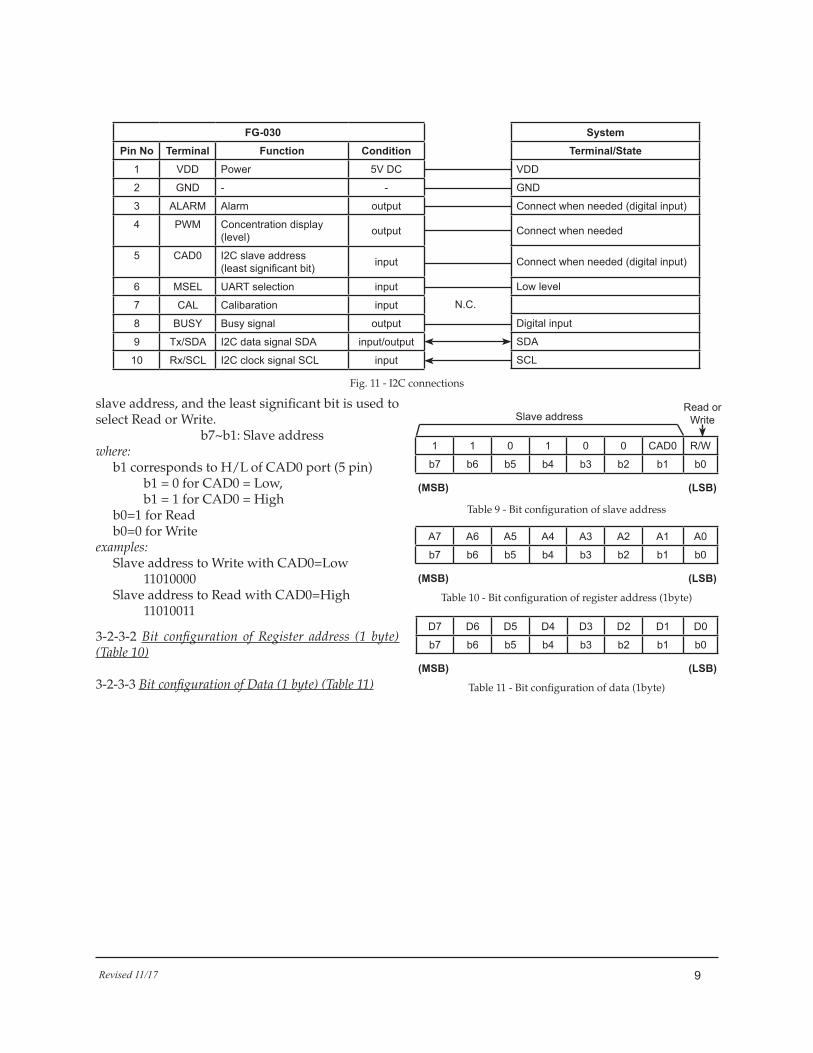
Revised 11/17 9
FG-030Pin No Terminal Function Condition
1 VDD Power 5V DC
2 GND - -
3 ALARM Alarm output
4 PWM Concentration display (level) output
5 CAD0 I2C slave address (least significant bit) input
6 MSEL UART selection input
7 CAL Calibaration input
8 BUSY Busy signal output
9 Tx/SDA I2C data signal SDA input/output
10 Rx/SCL I2C clock signal SCL input
SystemTerminal/State
VDD
GND
Connect when needed (digital input)
Connect when needed
Connect when needed (digital input)
Low level
Digital input
SDA
SCL
Fig. 11 - I2C connections
slave address, and the least significant bit is used to select Read or Write.
b7~b1: Slave addresswhere:
b1 corresponds to H/L of CAD0 port (5 pin)b1 = 0 for CAD0 = Low,b1 = 1 for CAD0 = High
b0=1 for Readb0=0 for Write
examples:Slave address to Write with CAD0=Low 11010000Slave address to Read with CAD0=High
11010011
3-2-3-2 Bit configuration of Register address (1 byte)(Table 10)
3-2-3-3 Bit configuration of Data (1 byte) (Table 11)
1 1 0 1 0 0 CAD0 R/W
b7 b6 b5 b4 b3 b2 b1 b0
(MSB) (LSB)
Slave addressRead or
Write
Table 9 - Bit configuration of slave address
A7 A6 A5 A4 A3 A2 A1 A0
b7 b6 b5 b4 b3 b2 b1 b0
(MSB) (LSB)
Table 10 - Bit configuration of register address (1byte)
D7 D6 D5 D4 D3 D2 D1 D0
b7 b6 b5 b4 b3 b2 b1 b0
(MSB) (LSB)
Table 11 - Bit configuration of data (1byte)
N.C.

Revised 11/17 10
3-2-4-1 Write commandFig.12 shows the data transfer sequence for theWrite command. In this sequence, “06H” is writtenat register address “01H” for setting continuousoperating mode. When CAD0=Low, the Slave address is 110100.
For details about the Start bit, Stop bit, ACK, and NACK, please refer to the document FG-030 Communication Specifications.
3-2-4-2 Read commandThere are two Read commands:
1) current address read command2) random read command.
Fig.13 shows the random read command. The data transmission sequence shows how CO2 concentration is read from FG-030. The random Read comand assigns “03H” as the register address and reads 2 bytes from the address. 3-2-5 Register memory map (Table 12, 13)Please refer to the document FG-030 CommunicationSpecifications for information about each registervalue, functions, and factory default setting.
4. Housing DesignCO2 gas enters the chamber of FG-030 through apin hole under the non-woven fabric as shownin Fig. 3. For gas diffusion, it is recommended toseparate the device housing from the top of the non-woven fabric by 5mm or more. If quicker responseis required, it is recommended that the gas inlet ofthe sensor be located at the device's slits/opening. Itis also recommended to make a small compartmentwith slits in at least two sides as shown in Fig. 14.
Sta
rt
AC
K
AC
K
AC
KS
top
Slave
Data transferfrom Master side:
: Data transfer from Master side
: Data transfer from Slave sideR / W = “0”
SDA
11010000 00000001 00000110
Register DataS PAddress Address(n)
Fig. 12 - Data transfer sequence for Write command
Sta
rt
Sta
rt
AC
K
AC
K
AC
K
AC
K
AC
K
AC
K
NA
CK
Sto
p
: Data transfer from Master side
: Data transfer from Slave side
R / W = “0” R / W = “1”
Data transferfrom Master side :
Data transfer
Register address:
CO2 concentration:
from Slave side :
11010000
10010000(90 H)
03H
01 90 H = 400 ppm
04H
(01 H)00000001
1101000100000011
SDAData(n) Data(n+1) Data(n+x)
SS PSlaveAddress
SlaveAddress
RegisterAddress(n)
Fig. 13 - Data transfer sequence for random Read command
1) Sensor compartment
2) Slits
Fig. 14 - Example housing design

Revised 11/17 11
Address Name REG/EEP Function Description00H RST REG Sofware reset Resets the module
01H CTL EEP Operating mode Specifies operating mode
02H ST1 REG Status register Monitors the operating status--read-only
03H DAL REG Low-order CO2 concentration data Read-only
04H DAH REG High-order CO2 concentration data Read-only
09H HPA EEP Atmospheric pressure Specifies atmospheric pressure
0AH HIT EEP Altitude Specifies altitude
0CH ALHI EEP Upper limit concentration for alarm signal Specifies upper limit cocentration for alarm signal
0DH ALLO EEP Lower limit concentration for alarm signal Specifies lower limit concentration for alarm signal
0EH CAL REG User calibration User calibration with I2C
0FH FUNC EEP PWM outputSpecifies properties of PWM function, enables/disables PWM, compensates atmospehric pressure and altitude
10H ERROR REG Self diagnosis (error output) Read-only
12H AJCON EEP CO2 concentration for user calibration Specifies CO2 concentration (400ppm default)
Address Name D7 D6 D5 D4 D3 D2 D1 D000H RST - - - - - - - REST
01H CTL - - - - - CTL2 CTL1 CTL0
02H ST1 BUSY ALARM - - - - CAD0 MSEL
03H DAL D7 D6 D5 D4 D3 D2 D1 D0
04H DAH - D14 D13 D12 D11 D10 D9 D8
09H HPA Hpa7 Hpa6 Hpa5 Hpa4 Hpa3 Hpa2 Hpa1 Hpa0
0AH HIT Hit7 Hit6 Hit5 Hit4 Hit3 Hit2 Hit1 Hit0
0CH ALHI Alhi7 Alhi6 Alhi5 Alhi4 Alhi3 Alhi2 Alhi1 Alhi0
0DH ALLO Allo7 Allo6 Allo5 Allo4 Allo3 Allo2 Allo1 Allo0
0EH CAL - - - - - - Zero-A Air-A
0FH FUNC - - - - PWMR HPAE - PWME
10H ERROR - - - - - - - Error0
12H AJCON Ajcon7 Ajcon6 Ajcon5 Ajcon4 Ajcon3 Ajcon2 Ajcon1 Ajcon0
Table 13 - Register map
Table 12 - Register table
Heat is generated at the internal optical source of FG-030. If a temperature sensor is located near the gas sensor, the temperature sensor may not show the correct ambient temperature. In this case, it is recommended to locate a temperature sensor where there is no thermal influence by FG-030. Maintain enough distance from the CO2 sensor or separate the temperature sensor from the CO2 sensor (e.g. by using a thermal insulator).
5. Packing (Fig. 15--see p. 12)50pcs. (25pcs. x 2 layers) of the individually wrappedFG-030 with antistatic bubble sheet is packed in aninner box. 10 inner boxes (FG-030: 50pcs. x10boxes) are packed in a carton box.
6. MaintenanceThe single light source, dual wavelength systememployed by the FG-030 measures light intensities attwo different wavelengths after separation bytwo optical filters, thus compensating drift due to
accumulated dust and contamination. As a result, there is no need for maintenance.
However, for customers who would like to calibrate periodically, the sensor has a function for air adjustment and zero adjustment. For more detail, please refer to Sec. 1-8-6. Pin No.7 (CAL).
7. Handling Precautions7-1 FG-030 is an ESD-sensitive product. No ESDprotection components such as zener diodes orvaristors are used in this product. It is recommended that ESD protection equipment be used for handlingthe module during assembly of application products. ESD protection components and/or an ESD protection enclosure should be used as required for the intended application when this module is embedded intofinished products.
7-2 If sensors are dropped, please do not use them.Sensors may be damaged by mechanical shock.

Revised 11/17 12
8. Frequently Asked QuestionsQ1: Is it possible to measure up to 10,000ppm? Can400ppm or less concentration be measured?A: The measurable CO2 concentration output rangethrough communication is from 0~10,000ppm.However, accuracy may be less than specificationsat less than 300ppm or higher than 5,000ppm. Themaximum PWM output range is 5,000ppm.
Q2: What kind of component is used for the optical source and detector element?A: A incandescent lamp is used as an optical source and a photodiode is used for the detector element.
Q3: There is a hysteresis by 100ppm between the high and low alarm thresholds. Is it possible to change the hysteresis?A: Yes, hysteresis can be changed. Please refer to “ALHI and ALLO” register of Register and EEPROM in the document FG-030 Communication Specifications.
Q4: Can the sensor be operated by 3V?A: No.
Q5: Can analog output be obtained?A: By converting the PWM output signal, an analog output voltage can be easily made. Please refer to Fig. 4 in Sec. 1-8-3 Pin No.4 (PWM).
Q6: What is the sensor's life expectancy?A: Expected sensor life of FG-030 is 10 years or more.
IMPORTANT NOTICEThis product is designed for use in indoor air quality control systems, including variable air volume systems and demand controlled ventilation systems. Please consult Figaro prior to use of this product in other applications. This product is not designed and authorized for use as a critical component in life support applications wherein a failure or malfunction of the products may result in injury or threat to life.
Figaro Engineering Inc. reserves the right to make changes without notice to this product to improve reliability, functioning or design.
REV.12/17 1
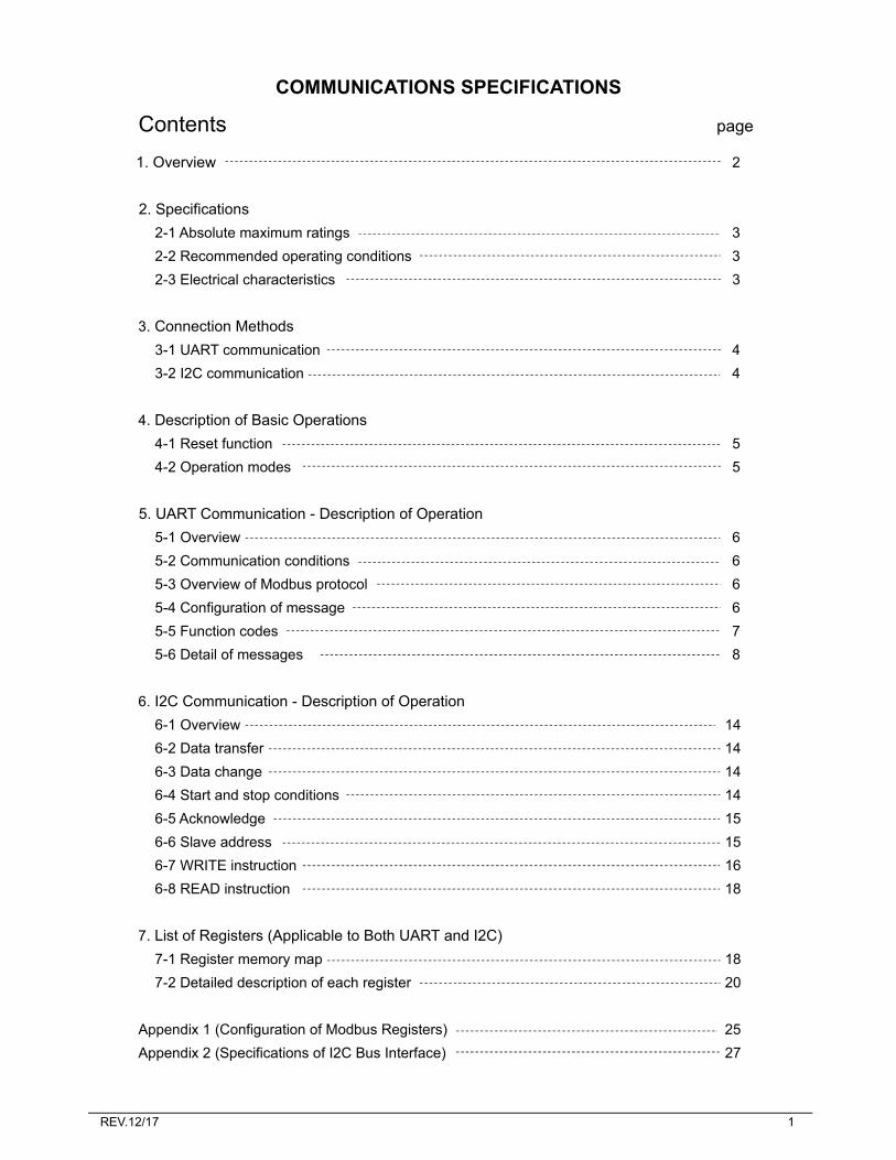
COMMUNICATIONS SPECIFICATIONS
Contents page
1. Overview 2
2. Specifications2-1 Absolute maximum ratings 32-2 Recommended operating conditions 3 2-3 Electrical characteristics 3
3. Connection Methods3-1 UART communication 4 3-2 I2C communication 4
4. Description of Basic Operations4-1 Reset function 5 4-2 Operation modes 5
5. UART Communication - Description of Operation5-1 Overview 65-2 Communication conditions 6 5-3 Overview of Modbus protocol 6 5-4 Configuration of message 6 5-5 Function codes 7 5-6 Detail of messages 8
6. I2C Communication - Description of Operation6-1 Overview 146-2 Data transfer 146-3 Data change 14 6-4 Start and stop conditions 14 6-5 Acknowledge 15 6-6 Slave address 156-7 WRITE instruction 166-8 READ instruction 18
7. List of Registers (Applicable to Both UART and I2C)7-1 Register memory map 18 7-2 Detailed description of each register 20
Appendix 1 (Configuration of Modbus Registers) 25 Appendix 2 (Specifications of I2C Bus Interface) 27

REV.12/17 2
The CDM7160 can control communication with the external controller and the I2C bus or the UART
interface and obtain CO2 concentration. Use the MSEL pin to select the I2C bus or UART.(1) MSEL = L
I2C bus interface is used for communication with the controller.
(2) MSEL = HUART interface is used for communication with the controller.
*The MSEL pin is a pull-up input. If this pin is not connected, the UART interface is used.
1. Overview

REV.12/17 3
2-1 Absolute maximum ratingsVss = 0 V
Item Sign Min. Max. Unit
Source voltage (Vdd) V;+ -0.3 +6.5 V
Input voltage VIN -0.3 (V+)+0.3 V
Input current IIN - ±10 mA
Storage temperature TST -30 +70 ˚C
(Note 1) If one or more of these values are exceeded during use, the module could be damaged.In such case, normal operation is not guaranteed.
2-2 Recommended operating conditionsVss = 0 V
Item Remark Sign Min. Typ. Max. Unit
Operation temperature Ta 0 +50 ˚C
Source voltage Vdd 4.75 5.0 5.25 V
2-3 Electrical characteristicsUnless otherwise specified, the following conditions are used: Vdd = 4.75V ~ 5.25V, Temperature range = 0˚C ~ 50˚C
DC characteristicsItem Sign Pin Condition Min. Typ. Max. Unit
High-level input voltage 1
VIH1 MSEL CAL
CAD0 CAD1
RX
80%Vdd V
Low-level input voltage 1
VIL1 20%Vdd V
Input current IIN -125 +125 nA
High-level input voltage 2
VIH2 SDA SCL
70%Vdd V
Low-level input voltage 2
VIL2 30%Vdd V
Low-level output voltage 1
VOL1 UART_R/T ALARM PWM
TX
(Note 2) 0.6 V
High-level output voltage
VOH (Note 3) Vdd-0.7 V
Low-level output voltage 2
VOL2 SDA (Note 2) 0.6 V
Power consumption IDD1
VDD Power down mode - - μA
IDD2 Continuous operation mode 1
8 60 mA
(Note 2) IOL = 8 mA, Vdd = 5V (Note 3) IOH = 3.5 mA, Vdd = 5V
2. Specifications

REV.12/17 4
3-1 UART communication
CDM7160
Pin No. Pin name Function Status
1 VDD Power supply DC +5V
2 GND - -
3 ALARM Alert output
4 PWM Concentration display (level) output
5 CAD0 I2C slave address (least significant)
input
6 MSEL Select I2C or UART input
7 CAL Calibration input
8 BUSY Busy signal output
9 Tx/SDA Tx output
10 Rx/SCL Rx input
3-2 I2C communication
Operation sequence from the viewpoint of the external controller (master) (1) Send the start condition(2) Send the slave address(3) Receive acknowledgement (abbreviated as Ack.) from the CDM7160(4) Send the register address to be accessed(5) Receive acknowledgement (abbreviated as Ack.) from the CDM7160(6) Repeat steps (4) and (5)(7) Send the stop bit
External controller
Pin/status
VDD
GND
Connect this pin as needed (digital output)
Connect this pin as needed
Connect this pin as needed (digital output)
Rx
Tx
CDM7160
Pin No. Pin
name
Function Status
1 VDD Power supply DC +5V
2 GND - -
3 ALARM Alert output
4 PWM Concentration display (level) output
5 CAD0 I2C slave address (least
significant) input
6 MSEL Select I2C or UART input
7 CAL Calibration input
8 BUSY Busy signal output
9 Tx/SDA I2C data signal SDA input/output
10 Rx/SCL I2C clock signal SCL input
External controller
Pin/status
VDD
GND
Connect this pin as needed (digital output)
Connect this pin as needed
Connect this pin as needed (digital input)
Low level
Digital output
SDA
SCL
Figure 1 - UART Communication Connection
Figure 2 - I2C Communication Connection
3. Connection Methods
N.C.
N.C.
N.C.
N.C.

REV.12/17 5
4-1 Reset function (applicable to both UART and I2C)
The CDM7160 is reset when the power is turned on. The CDM7160 also has a soft reset function.Soft reset
The CDM7160 can be reset by writing 1 to the REST bit in the RST register through the UART interface. When reset is complete, the REST bit automatically returns to 0.
4-2 Operation modes (applicable to both UART and I2C)
CDM7160 has the following two operation modes:(1) Power down mode(2) Continuous operation mode 1The corresponding operation mode can be activated by setting a value in the CTL register.
(1) Power down modeThe master clock stops and all analog circuits are turned off.
(2) Continuous operation mode 1When continuous operation mode 1 is set, analog circuits start operating. The following series ofoperations will commence:
A) First, measurement of CO2 concentration starts after a determined setup time. At this time, 1 is setto the BUSY bit in the ST1 register and H is set to the BUSY pin.
B) The first measurement of CO2 concentration ends after about 0.3 sec. At this time, 0 is set to theBUSY bit in the ST1 register and L is set to the BUSY pin.Immediately thereafter, the analog circuit stops and enters into low power consumption mode.
C) After 1.7 seconds, the analog circuits operate again and automatically start measuring CO2concentration. At this time, 1 is set to the BUSY bit in the ST1 register and H is set to the BUSY pin.
D) This measurement of CO2 concentration ends after about 0.3 seconds and 0 is set to the BUSY bitin the ST1 register and L is set to the BUSY pin. CO2 concentration data is now ready to be read.External devices can detect this change and read the concentration data from the DAL and DAHregisters.Immediately thereafter, the analog circuit stops and enters into low power consumption mode.After this, repeat step C) -- measurement is done again.Measurement is repeated until operation mode is changed by overwriting the value in the CTLregister.
*To change the alarm and other settings, switch to power down mode, change set conditions, and moveback to continuous operation mode.
The operation sequence is shown in the figure below:
Figure 3 - Continuous Operation Mode
Continuous operation mode 1
2 s0.3 s
BUSY
Concentration data can be read.
4. Description of Basic Operations

REV.12/17 6
5-1 Overview
When H is set on the MSEL pin, the CDM7160 uses UART communication mode. As the UART interfaceis used for communication with the external controller, the TX/SDA pin and the RX/SCL pin operate as TXand RX, respectively, with the communication protocol based on the Modbus protocol.For details on Modbus specifications, refer to www.modbus.org.
5-2 Communication conditions
UART communication by the CDM7160 supports only the following limited specifications:(1) Only the RTU mode to send 1-byte (8-bit) data is supported. ASCII mode is not supported.(2) Supported communication speed is 9600 bps only.(3) Both for transmission and reception, no parity bit is used, the start bit is 1 bit, and the stop bit is 1 bit.
The logic of the start bit is L while the logic of the stop bit is H.
(Reference) A 10-bit data string used to send 1-byte data is defined as one character. The time to send one character is about 1.04 ms at 9600 bps.
5-3 Overview of Modbus protocol
According to Modbus protocol, the master always sends messages while the slave responds to them.The controller is the master device while the CDM7160 is the slave device.The transmission procedure is as follows:
(1) The master sends the command message to the slave.(2) The slave checks if the device address contained in the received message matches its localstation.(3) When the device address matches, the slave performs processing according to the function codeand returns a response message.(4) When the device address does not match, the slave discards the received message and waits forthe next message.
3.5 or more space characters are required before and after each message.1.5 or less space characters are required between characters in the message.
5-4 Configuration of messageThe command message from the master and the response message from the slave consist of four
sections: device address, function code, data section, and error check code, which are sent in this order.Each of these sections is described below:
1. Device address (1 byte)Number to identify the slave. For the time being, only FEH, which corresponds to all addresses, issupported.
2. Function code (1 byte)Code to specify the function to be executed by the slave.For details, refer to "5-5 Function codes."
3. Data section (2 to 17 bytes)Data required to complete the function code. The configuration of the data section differs depending onthe function code. For details, refer to "5-6 Details of messages."
4. Error check code (2 bytes)Code to detect errors in the message during signal transmission.
5. UART Communication - Description of Operation

REV.12/17 7
CRC16-IBM (Rightward transmission, Initial value: 0xFFFF, Generating polynomial value: 0xA001) is used in the RTU mode for Modbus protocol. The calculation range is from the start of the message (device address) to the end of the data section. The slave calculates the CRC of the received message and does not respond if it does not match the received CRC code.
Device address Function code Data section Error check code (CRC-16) 1 byte 1 byte 2 to 17 bytes 2 bytes
Configuration of Message
5-5 Function codes
The CDM7160 only supports the six types of function codes shown in the table below. The length of the data section differs depending on the function code.
Function Codes
Param. No. Length of data section
Function code Function Target Command Response
(at normal time)
03H Read Holding register 4 bytes 3 to 17 bytes
Checks the CAL execution status with UART
04H Read Input register 4 bytes 3 to 17 bytes
Reads CO2 concentration data with UART
06H Write Holding register 4 bytes 4 bytes Executes CAL with UART
44H Read CO2 concentration data 3 bytes 2 to 17 bytes
Dedicated to reading CO2 concentration data with UART
64H Write Register for CDM7160 2 bytes 2 bytes Writes the register value
with UART
65H Read Register for CDM7160 2 bytes 2 to 17 bytes Reads the register value
with UART

REV.12/17 8
5-6 Details of messages
This section individually describes each function code.
Reading from the holding register [Function code: 03H]
Structure of command message Message structure (byte) Example Remark Device address FEH All devices Function code 03H
Read start address High-order 00H Low-order 00H
Number of read words High-order 00H
Up to 8 words (16 bytes) Low-order 01H
CRC data High-order 90H Low-order 05H
Structure of response message At normal time
Message structure (byte) Example Remark Device address FEH All devices Function code 03H Number of read bytes 02H Number of words ×2
First read data High-order 00H Contents at address 0
Acknowledgment register Low-order 20H
CRC data Low-order ADH High-order 88H
When read start address > 001FH or (Read start address + Number of read words) > 0020H Message structure (byte) Example Remark Device address FEH All devices Function code 83H Exception code 02H Illegal Data Address
CRC data Low-order F0H High-order C1H
When the message length excluding CRC is not six bytes or when the number of read words is zero or larger than eight
Message structure (byte) Example Remark Device address FEH All devices Function code 83H Exception code 03H Illegal Data Value
CRC data Low-order 31H High-order 01H

REV.12/17 9
Reading from the input register [Function code: 04H]
Structure of command message Message structure (byte) Example Remark Device address FEH All devices Function code 04H
Read start address High-order 00H Low-order 00H
Number of read words High-order 00H
Up to 8 words (16 bytes) Low-order 04H
CRC data Low-order E5H High-order C6H
Structure of response message At normal time
Message structure (byte) Example Remark Device address FEH All devices Function code 04H Number of read bytes 08H Number of words ×2
First read data High-order 00H Contents at address 0
Meter Status Low-order 00H
Second read data High-order 00H Contents at address 1
Alarm Status Low-order 00H
Third read data High-order 00H Contents at address 2
Output Status Low-order 00H
Fourth read data High-order 01H Contents at address 3
CO2concentration Low-order 90H
CRC data Low-order 16H High-order E6H
When read start address > 001FH or (Read start address + Number of read words) > 0020H Message structure (byte) Example Remark Device address FEH All devices Function code 84H Exception code 02H Illegal Data Address
CRC data Low-order F2H High-order F1H
When the message length excluding CRC is not six bytes or when the number of read words is zero or larger than eight
Message structure (byte) Example Remark Device address FEH All devices Function code 84H Exception code 03H Illegal Data Value
CRC data Low-order 33H High-order 31H

REV.12/17 10
Writing to the holding register [Function code: 06H]
Structure of command message Message structure (byte) Example Remark Device address FEH All devices Function code 06H
Write start address High-order 00H Writes 0000H to address 0 Low-order 00H
Write data High-order 00H Low-order 00H
CRC data Low-order 9DH High-order C5H
Structure of response message At normal time
Message structure (byte) Example Remark Device address FEH All devices Function code 06H
Write address High-order 00H
Low-order 00H
Write data High-order 00H Returns written data Low-order 00H
CRC data Low-order 9DH High-order C5H
When write address > 1FH Message structure (byte) Example Remark Device address FEH All devices Function code 86H Exception code 02H Illegal Data Address
CRC data Low-order F3H High-order 91H
When the message length excluding CRC is not six bytes Message structure (byte) Example Remark Device address FEH All devices Function code 86H Exception code 03H Illegal Data Value
CRC data Low-order 32H High-order 51H

REV.12/17 11
Reading CO2 concentration data [Function code: 44H]
Structure of command message Message structure (byte) Example Remark Device address FEH All devices Function code 44H
Read start address High-order 00H Low-order 08H
Number of read bytes 02H
CRC data Low-order 9FH High-order 25H
*Only the message in the above command message example can be used.
Structure of response message At normal time
Message structure (byte) Example Remark Device address FEH All devices Function code 44H Number of read bytes 02H
CO2 concentration data High-order 01H Contents at address 3 (CO2
concentration) is indirectly read Low-order 90H
CRC data Low-order B9H High-order 18H
When read start address > 03FFH or (Read start address + Number of read words) > 0400H Message structure (byte) Example Remark Device address FEH All devices Function code A4H Exception code 02H Illegal Data Address
CRC data Low-order EBH High-order 31H
When the message length excluding CRC is not five bytes or when the number of read bytes is 0 Message structure (byte) Example Remark Device address FEH All devices Function code A4H Exception code 03H Illegal Data Value
CRC data Low-order 2AH High-order F1H

REV.12/17 12
Writing to the register for CDM7160 [Function code: 64H]
Structure of command message Message structure (byte) Example Remark Device address FEH All devices Function code 64H CDM7160 unique code Write address 01H
Write data 06H Writes to address 1
CTL: Control
CRC data Low-order F1H High-order 81H
Structure of response message At normal time
Message structure (byte) Example Remark Device address FEH All devices Function code 64H CDM7160 unique code Write address 01H Write data 06H Returns written data
CRC data Low-order F1H High-order 81H
When write address > 0FH Message structure (byte) Example Remark Device address FEH All devices Function code E4H Exception code 02H Illegal Data Address
CRC data Low-order DAH High-order F1H
When the message length excluding CRC is not four bytes Message structure (byte) Example Remark Device address FEH All devices Function code E4H Exception code 03H Illegal Data Value
CRC data Low-order 1BH High-order 31H
The writable address range is from 00H to 0FH.

REV.12/17 13
Reading from the register for CDM7160 [Function code: 65H]
Structure of command message Message structure (byte) Example Remark Device address FEH All devices Function code 65H CDM7160 unique code Read start address 00H Number of read bytes 05H Up to 16 bytes
CRC data Low-order E1H High-order D0H
Structure of response message At normal time
Message structure (byte) Example Remark Device address FEH All devices Function code 65H CDM7160 unique code Number of read bytes 05H First read data 00H RST: Software reset
Second read data 06H CTL: Control
Third read data 01H ST1: Status 1 Fourth read data 90H DAL: Low-order CO2
concentration data Fifth read data 01H DAH: High-order CO2
concentration data
CRC data Low-order 07H High-order 18H
When write address > 0FH Message structure (byte) Example Remark Device address FEH All devices Function code E5H Exception code 02H Illegal Data Address
CRC data Low-order DBH High-order 61H
When the message length excluding CRC is not four bytes or when (Read start address + Number of read bytes) > 0FH
Message structure (byte) Example Remark Device address FEH All devices Function code E5H Exception code 03H Illegal Data Value
CRC data Low-order 1AH High-order A1H
The readable address range is from 00H to 0FH.

REV.12/17 14
6-1 OverviewWhen the MSEL pin is set to L, CDM7160 operates with I2C communication. As the I2C bus interface is
used for communication with the external controller, the TX/SDA pin and the RX/SCL pin operate as SDAand SCL, respectively. The UART_R/T/BUSY pin operates as the BUSY signal output pin.
For the I2C bus interface in the CDM7160, standard mode (up to 100 kHz) or high-speed mode (up to 400kHz) can be selected. (For details on the I2C bus interface, refer to Appendix 2, "Specifications of I2C BusInterface" at the end of this document.)
6-2 Data transferThe start condition must be first input to access the CDM7160 via the bus.Next, the 1-byte slave address containing the device address is sent. At this time, the CDM7160 compares the received slave address with its own slave address. When these addresses match, the CDM7160 generates an acknowledgement and executes the read or write instruction. To end the instruction, input the stop condition.
6-3 Data change
SDA line data can be changed while the clock on the SCL line is at Low. While the clock signal on the SCL line is High, the status of the SDA line must be constant. (Data on the SDA line can be changed only while the clock signal on the SCL line is Low.)While the SCL line is High, the status of data on the SDA line is changed only when the start or stop condition is input.
Figure 4 - Data Change
6-4 Start and stop conditionsIf the SDA line is changed from High to Low while the SCL line is High, the start condition is generated.
All data transfer starts with the start condition.If the SDA line is changed from Low to High while the SCL line is High, the stop condition is generated.All data transfer ends with the stop condition.
Figure 5 - Start and Stop Conditions
Data can be changed.
SCL
SDA Data line is constant.
SCL
SDA
Start condition Stop condition
6. I2C Communication - Description of Operation

REV.12/17 15
6-5 Acknowledgement
The device that sends data opens the SDA line after sending 1-byte data (High status). The device thatreceives the data sets Low to the SDA line at the next clock. This operation is called acknowledgement.Acknowledgement allows checking if data transfer has been successfully completed.The CDM7160 generates acknowledgement after receiving the start condition and the slave address.When executing the WRITE instruction, CDM7160 generates acknowledgement when receiving each byte.When executing the READ instruction, CDM7160 generates acknowledgement and sends data stored atthe specified address. The CDM7160 then opens the SDA line and monitors it. If the master device generatesacknowledgement instead of the stop condition, the CDM7160 sends the 8-bit data stored at the nextaddress. If acknowledgement is not generated, the CDM7160 stops sending data.
Figure 6 - Generation of Acknowledgement
6-6 Slave address
The first byte containing the slave address is input after the start condition. The slave address is used toselect the device to be accessed from the devices on the bus.The slave address consists of the upper 7 bits. The upper 6 bits of the slave address are fixed to 110100 inthe CDM7160. The 7th bit is the address bit to select the device to be accessed and is set by the CAD0 pin.When the slave address is input, the device whose address matches generates acknowledgement and thenexecutes the instruction. The eighth bit (the least significant bit) in the first byte is the R/W bit.When the R/W bit is 1, the READ instruction is executed. When the R/W bit is 0, the WRITE instruction isexecuted.
Figure 7 - Slave Address
1 1 0 1 0 0 CAD0 R/W
SCL from the master
Data output from the sending side
Data output from the receiving side
Start condition
1 8 9
Clock pulse for acknowledgement
Acknowledge
Non acknowledge
MSB LSB

REV.12/17 16
6-7 WRITE instruction <applicable to the register and EEPROM>
When 0 is set to the R/W bit, the CDM7160 executes the write operation.During the write operation, the CDM7160 receives the start condition and the first byte (slave address),generates acknowledgement, and then receives the second byte. The second byte specifies the address ofthe internal control register in the MSB first format.
Figure 8 - Register Address
After receiving the second byte (register address), the CDM7160 generates acknowledgement and then receives the third byte.The third byte represents control data. Control data consists of 8 bits in the MSB first format. After receiving control data, the CDM7160 generates acknowledgement. Data transfer always ends with the stop condition generated by the master.
Figure 9 - Control Data
The CDM7160 does not support sequential write. The CDM7160 writes data under the stop condition.If the specified address is write-only, data is not written.
Figure 10 - Write
If the specified address points to EEPROM, the CDM7160 generates acknowledgement after the slave address is sent and after the register address is sent.If the CDM7160 receives data afterward, clock stretch occurs to ensure the EEPROM write time (Note 1).When clock stretch ends and SCL is released, the master device generates the stop condition and the write operation ends.
Note 1) The CDM7160 delays the processing at the master device to ensure the EEPROM write time by forcibly setting L to SCL.
Figure 11 - Write (EEPROM)
A7 A6 A5 A4 A3 A2 A1 A0
D7 D6 D5 D4 D3 D2 D1 D0
MSB LSB
MSB LSB
SDA Slave Address
Stop
Register Address(n)
Data S P
ACK
Star
t
ACK
ACK
R/W=0
SDA Slave Address
Register Address(n)
Data(n) S P
START
R/W="0" STOP
Slave AddressS
START
R/W="0"
Twr. 10ms~
100ms
ACK
ACK
ACK
ACK

REV.12/17 17
6-8 READ instruction <applicable to the register and EEPROM>When 1 is set to the R/W bit, the CDM7160 executes the read operation.If the master device generates acknowledgement instead of the stop condition after the CDM7160 sendsthe data from the specified address, data can be read from the next address.Once the address is counted up to 0FH in the range between 00H and 0FH, the next address returns to 00H.
(1) Reading data from the current addressThe CDM7160 has an internal address counter. During the operation to read data from the currentaddress, data is read from the address specified at this counter.The internal address counter retains the address next to the last accessed address.For example, if the last accessed address for the READ instruction is n, data is read from address n+1when the instruction to read data from the current address is executed.When reading data from the current address, the CDM7160 receives the slave address for the READinstruction (R/W bit = 1) and generates acknowledgement. Then, the CDM7160 starts transferring dataspecified at the internal address counter at the next clock and increments the internal address counterby 1. If the master device generates the stop condition instead of acknowledgement after the CDM7160sends 1-byte data, the read operation ends.
Figure 12 - Reading Data from the Current Address
(2) Random readThe random read operation reads data from an arbitrary address.For random read, the WRITE instruction must be executed as dummy before the slave address for the READinstruction (R/W bit = 1) is sent. During the random read operation, the start condition is first generated andthen the slave address for the WRITE instruction and the read address are sent. In response to this addresstransmission, the CDM7160 generates acknowledgement and then the master device sends the startcondition and the slave address for the READ instruction (R/W bit = 1) again. The CDM7160 generatesacknowledgement in response to this transmission of slave address. After that, the CDM7160 sends datafrom the specified address and increments the internal address counter by 1.If the master device generates the stop condition instead of acknowledgement after sending data, the readoperation ends.
Figure 13 - Random Read
SDA Slave Address
Data(n+1) S
START
R/W="1" STOP
P Data(n) Data(n+2) Data(n+x)
ACK
ACK
ACK
ACK
ACK
SDA Slave AddressS
START
R/W="0" STOP
P Register Address(n)
Data(n) Data(n+x)
ACK
ACK
ACK
ACK
ACK
Slave AddressS Data(n+1)
ACK
R/W="1" START

REV.12/17 18
7-1 Register memory mapThe CDM7160 has the registers and EEPROM with the addresses shown in Table 1. Each address consists of8-bit data.
Address Name REG/EEP* Brief description Description
00H RST REG Soft reset Resets the module
01H CTL EEP Operation mode Sets the operation mode
02H ST1 REG Status register Monitors the operation state. Read-only
03H DAL REG Lower CO2 concentration data Read-only
04H DAH REG Upper CO2 concentration data Read-only
05H - Reserved Read/write not allowed
06H - Reserved Read/write not allowed
07H - Reserved Read/write not allowed
08H - Reserved Read/write not allowed
09H HPA EEP Atmospheric pressure data Sets the atmospheric pressure value (hPa)
0AH HIT EEP Altitude data Sets the altitude value (m)
0BH - Reserved Read/write not allowed
0CH ALHI EEP Upper limit concentration for the alarm signal
Sets the upper limit concentration for the alarm signal
0DH ALLO EEP Lower limit concentration for the alarm signal
Sets the lower limit concentration for the alarm signal
0EH CAL REG User calibration User calibration with I2C
0FH FUNC EEP Control of each type of function Sets correction for PWM output, atmospheric pressure and altitude
10H ERROR REG Self-diagnosis (error output) Read-only
11H - Reserved Read/write not allowed
12H AJCON EEP CO2 concentration for user calibration Sets the CO2 concentration. (400 ppm set by default)
Table 1 = Register Table
*REG: The data in the register is initialized when the power is turned off.EEP: The data in the register is retained even when the power is turned off.
7. List of Registers (Applicable to Both UART and I2C)

REV.12/17 19
Register mapAddress Name D7 D6 D5 D4 D3 D2 D1 D0
00H RST - - - - - - - REST
01H CTL - - - - - CTL2 CTL1 CTL0
02H ST1 BUSY ALARM - - - - CAD0 MSEL
03H DAL D7 D6 D5 D4 D3 D2 D1 D0
04H DAH - D14 D13 D12 D11 D10 D9 D8
05H - - - - - - - - -
06H - - - - - - - - -
07H - - - - - - - - -
08H - - - - - - - - -
09H HPA Hpa7 Hpa6 Hpa5 Hpa4 Hpa3 Hpa2 Hpa1 Hpa0
0AH HIT Hit7 Hit6 Hit5 Hit4 Hit3 Hit2 Hit1 Hit0
0BH - - - - - - - - -
0CH ALHI Alhi7 Alhi6 Alhi5 Alhi4 Alhi3 Alhi2 Alhi1 Alhi0
0DH ALLO Allo7 Allo6 Allo5 Allo4 Allo3 Allo2 Allo1 Allo0
0EH CAL - - - - - - Zero-A Air-A
0FH FUNC - - - - PWMR HPAE - PWME
10H ERROR - - - - - - - Error0
12H AJCON Ajcon7 Ajcon6 Ajcon5 Ajcon4 Ajcon3 Ajcon2 Ajcon1 Ajcon0
Table 2 - Register Map
Note) Do not write or read data to or from an address other than those above.

REV.12/17 20
7-2 Detailed register descriptions
RST: Soft reset
Address Register name D7 D6 D5 D4 D3 D2 D1 D0 Write/read
00H RST - - - - - - - REST
REST: Reset0: Normal status1: Reset
The CDM7160 is reset when 1 is written to this bit. When reset ends, this bit automatically returns to 0.
CTL: Control
Address Register name D7 D6 D5 D4 D3 D2 D1 D0 Write/read EEPROM
01H CTL - - - - - CTL2 CTL1 CTL0 Reset 0 0 0 0 0 1 1 0
CTL<2:0>: Specification of operation modeSet value Operation mode
D2 D1 D0 0 0 0 Power down mode 1 1 0 Continuous operation mode
*Note: Do not write a value other than 00H or 06H to the CTL register.
ST1: Status 1
Address Register name D7 D6 D5 D4 D3 D2 D1 D0 Read-only register
02H ST1 BUSY ALARM - - - - CAD0 MSEL Reset 0 0 0 0 0 0 0 0
BUSY: Busy0: Data can be read.1: Busy status
The BUSY bit becomes 1 if data cannot be read--for example, during ADC conversion or operation of read data. The controller reads data after confirming that this bit changed from 1 to 0.The status of this bit is output to the BUSY pin as well.
ALARM: Alarm0: The CO2 concentration is below 10 times the CO2LO value.1: The CO2 concentration is above 10 times the CO2HI value.
The ALARM bit notifies that the CO2 concentration exceeds the preset value.The status of this bit is output to the ALARM pin as well.
CAD0, MSEL:
Can monitor the status of the CAD0 and MSEL pins.*If there is no connection to the CAD0 pin, the CAD0 is internally pulled up to High status.

REV.12/17 21
DAL to DAH: CO2 concentration data
Address Register name D7 D6 D5 D4 D3 D2 D1 D0 Read-only register
03H DAL D7 D6 D5 D4 D3 D2 D1 D0 04H DAH - D14 D13 D12 D11 D10 D9 D8
Reset 0 0 0 0 0 0 0 0
CO2 concentration data is output to D0 to D14. Concentration data is stored in little endian.The data range is from 0 to 10000 in decimal notation.
CO2 concentration data CO2 concentration data Binary Hexadecimal Decimal
X010 0111 0001 0000 2710 10000 10000ppm | | | |
X000 0000 0000 0000 0000 0 0ppm
If the concentration is 400 ppm, DAL = 90H and DAH = 01H.
ALHI: ALARM high threshold data
Address Register name D7 D6 D5 D4 D3 D2 D1 D0 Write/read EEPROM
0CH ALHI Alhi7 Alhi6 Alhi5 Alhi4 Alhi3 Alhi2 Alhi1 Alhi0 At shipment 0 1 1 0 0 1 0 0
This register sets the CO2 concentration at which the ALARM bit changes from 0 to 1. When the CO2 concentration data exceeds 10 times the value written to this register, the ALARM bit changes to 1. If ALHI = 64H, the ALARM bit changes to 1 when the CO2 concentration exceeds 1000 ppm.
ALLO: ALARM low threshold data
Address Register name D7 D6 D5 D4 D3 D2 D1 D0 Write/read EEPROM
0DH ALLO Allo7 Allo6 Allo5 Allo4 Allo3 Allo2 Allo1 Allo0 At shipment 0 1 0 1 1 1 0 0
This register sets the CO2 concentration at which the ALARM bit changes from 1 to 0. When the CO2 concentration data drops below 10 times the value written to this register, the ALARM bit changes to 0. If ALLO = 5AH, the ALARM bit changes to 0 when the CO2 concentration drops below 900 ppm.You can add hysteresis by setting a value larger than ALLO to ALHI.Set a value equal to or larger than ALLO to ALHI.

REV.12/17 22
HPA: hPa (atmospheric pressure)
Address Register name D7 D6 D5 D4 D3 D2 D1 D0 Write/read EEPROM
09H HPA Hpa7 Hpa6 Hpa5 Hpa4 Hpa3 Hpa2 Hpa1 Hpa0 At shipment 1 1 0 1 0 1 0 1
Write the atmospheric pressure data to correct atmospheric pressure when calculating CO2 concentration. The atmospheric pressure data is expressed as follows: Atmospheric pressure (hPa) = HPA + 800 When HPA = D5H, the atmospheric pressure is 1013 hPa.
HPA data Atmospheric pressure Binary Hexadecimal Decimal
1111 1111 FF 255 1055 hPa | | | |
0000 0000 00 0 800 hPa
HIT: Height (altitude)
Address Register name D7 D6 D5 D4 D3 D2 D1 D0 Write/read EEPROM
0AH HIT Hit7 Hit6 Hit5 Hit4 Hit3 Hit2 Hit1 Hit0 At shipment 0 0 0 0 0 0 0 0
Write altitude data to correct the atmospheric pressure when calculating the CO2 concentration. The altitude data is expressed as follows: Altitude (m) = HIT×10
HIT data Altitude
Binary Hexadecimal Decimal 1111 1111 FF 255 2550 m
| | | |
0000 0000 00 0 0 m
Note: When writing altitude data, HIT - When writing the actual altitude (m) value, write the atmospheric pressure at 0 m above sea level to theatmospheric pressure data, HPA.- When the actual atmospheric pressure (hPa) value has been written to HPA: 0(m) (at the time ofshipment)(Reference): The atmospheric pressure correction value by altitude is simplified to be -1.1 hPa per 10m.
When using the atmospheric pressure and altitude correction functions, set 1 (enabled) to the HAPE bit in the FUNC register (address: 0FH).

REV.12/17 23
CAL: User calibration
Address Register name D7 D6 D5 D4 D3 D2 D1 D0 Write-only register
0EH CAL - - - - - - Zero-A Air-A Reset 0 0 0 0 0 0 0 0
Air-A: Air Adjustment is executed when the Air-A bit is set to 1 under normal clean atmosphere or to the CO2 concentration that is pre-set at the register address (12H). After execution of Air Adjustment, the measured concentration value is reset to the pre-set CO2 value at the register address (12H).
Zero-A: Zero Adjustment is executed when the Zero-A bit is set to 1 while the sensor is placed into zero gas. Measured concentration value is reset to 0ppm.
FUNC: Function setting
Address Register name D7 D6 D5 D4 D3 D2 D1 D0 Write/read EEPROM
0FH FUNC - - - - PWMR HPAE - PWMEAt shipment 0 0 0 0 0 0 0 1
This register enables/disables each type of function and sets other conditions.This register is not initialized even when CDM7160 is reset.
PWME: Enables/disables the PWM pin.0: Disable1: Enable
When 1 is set to the PWME bit, a 1-kHz square wave with a pulse width that is proportional to the CO2 concentration is output from the PWM pin.When 0 is set, the PWM pin is always at high impedance. You can reduce power consumption by setting 0 when not using the PWM pin.
PWMR: Sets the concentration range represented by the pulse width output to the PWM pin.0: High concentration1: Low concentration
The relationship between the concentration and the pulse width (PW) is expressed by the following expressions:
High concentration: Concentration (ppm) = PW (μs) × 5Low concentration: Concentration (ppm) = PW (μs) × 2
HPAE: Enables/disables atmospheric pressure correction.0: Disable 1: Enable
When 1 is set to the HPAE bit, the CO2 concentration is calculated after correcting the atmospheric pressure based on the data written to the HPA and HIT registers. When 0 is set, the CO2 concentration is calculated assuming an atmospheric pressure of 1013 hPa and altitude of 0m.

REV.12/17 24
ERROR: Self-diagnosis
Address Register name D7 D6 D5 D4 D3 D2 D1 D0 Read-only register
10H ERROR - - - - - - - Error0 Reset 0 0 0 0 0 0 0 0
Error0: Self-diagnosis error0: No self-diagnosis error1: Self-diagnosis error generated
The error bit indicates if an error occurred as a result of self-diagnosis. If there is no error, the error bit is 0. If an error occurred, the error bit is 1.
AJCON: User calibration adjustment concentration
Address Register name D7 D6 D5 D4 D3 D2 D1 D0 Write/read EEPROM
12H AJCON Ajcon7 Ajcon6 Ajcon5 Ajcon4 Ajcon3 Ajcon2 Ajcon1 Ajcon0
At shipment 0 0 0 0 1 0 1 0
This register sets the adjustment concentration (target concentration) when executing user calibration.The default value at the time of shipment is 400 ppm.
The adjustment concentration is expressed as follows: Adjustment concentration (ppm) = AJCON × 10 + 300
AJCON data Adjustment concentration Binary Hexadecimal Decimal
1111 1111 FF 255 2850ppm | | | |
0000 0000 00 0 300ppm

REV.12/17 25
The Modbus registers in CDM7160 consist of two independent register groups - input registers and holding registers. The tables below show their configuration. Both types of registers are defined by 32 16-bit addresses. Though accessing the reserved section does not cause an error, no operation is performed. Although the input register supports continuous read, data can be read from up to eight addresses at once. The address number is the value calculated by subtracting 1 from the register number.
Input registers
Input registers are read-only registers. Only IR4 is actually enabled. IR4 stores the measured CO2 concentration in ppm.
Register
No. Address Register Name
IR1~3 0 to 2 Reserved
IR4 3 CO2 concentration CO2 concentration/ppm
IR5~21 4 to 20 Reserved - returns “illegal data address” exception
IR22 21 Reserved
IR23~32 22 to 31 Reserved - returns “illegal data address” exception
Appendix 1 (Configuration of Modbus Registers)

REV.12/17 26
Holding registers
Only HR1 and HR2 are actually enabled. HR1 supports read/write while HR2 is write-only. Calibration starts when a value is written to HR2. When calibration is complete, the relevant bit in HR1 becomes 1. When performing calibration using HR1 and HR2, the following procedure is recommended:
(1) Write 0 to HR1. (2) Write 7C06H (air adjustment) or 7C07H (zero adjustment) to HR2. (3) Read HR1 and check that DI6 or DI7 is 1.
Register
No. Address Register Name
HR1 0 Acknowledgment register
DI 16
DI 15
DI 14
DI 13
DI 12
DI 11
DI 10
DI 9
DI 8
DI 7
DI 6
DI 5
DI 4
DI 3
DI 2
DI 1
DI1 DI2 DI3 DI4 DI5 DI6 - CO2 air adjustment has been performed DI6 DI7 - CO2 zero adjustment has been performed DI7 DI8 DI9 DI10 DI11 DI12 DI13 DI14 DI15 DI16
HR2 1 Special Command Register *
Command Parameter
7CH 06H - CO2 air adjustment 07H - CO2 zero adjustment
HR3~
32
2~31 Reserved - returns “illegal data address” exception

REV.12/17 27
The I2C bus interface supports the standard mode and the high-speed mode.
(1) I2C BUS START/STOP BITS TIMING
(2) I2C BUS START/STOP BITS REQUIREMENTS
Param.
No. Sign Item Min. Typ. Max. Unit Condition
SP90 TSU:STA Start Condition Setup time
100kHz mode 4700 - - ns
Only relevant for Repeated Start condition 400kHz mode 600 - -
SP91 THD:STA Start Condition Hold time
100kHz mode 4000 - -
ns
After this period, the first clock pulse is generated
400kHz mode 600 - -
SP92 TSU:STO Stop Condition Setup time
100kHz mode 4700 - - ns
400kHz mode 600 - -
SP93 THD:STO Stop Condition Hold time
100kHz mode 4000 - - ns
400kHz mode 600 - -
(3) I2C DATA TIMING
SCL
SDA
SP90 SP91
SP92 SP93
Start Condition Condition
Stop
SP100
SP90
SP91
SP103 SP102 SP101
SP107
SCL
SP106
SP92
SP110
SP109 SP109
In SDA
SDA Out
Appendix 2 (Specifications of I2C Bus Interface)

REV.12/17 28
(4) I2C BUS DATA REQUIREMENTS
Param. No. Sign Item Min. Max. Unit Condition
SP100 THIGH Clock high time
100kHz mode 4.0 - μs Device must operate at a minimum of 1.5MHz
400kHz mode 0.6 - μs Device must operate at a minimum of 10MHz
SSP module 1.5Tcy -
SP101 TLOW Clock low time
100kHz mode 4.7 - μs Device must operate at a minimum of 1.5MHz
400kHz mode 1.3 - μs Device must operate at a minimum of 10MHz
SSP module 1.5Tcy -
SP102 TR SDA and SCL rise time
100kHz mode - 1000 ns
400kHz mode 20+0.1C
B
300 ns CB is specified to be from 10-400pF
SP103 TF SDA and SCL fall time
100kHz mode - 250 ns
400kHz mode 20+0.1C
B
250 CB is specified to be from 10-400pF
SP106 THD:DAT Data input hold time
100kHz mode 0 -
400kHz mode 0 0.9
SP107 TSU:DAT Data input setup time
100kHz mode 250 - ns (Note2)
400kHz mode 100 - ns
SP109 TAA Output valid from clock
100kHz mode - 3500 ns (Note1)
400kHz mode - - ns
SP110 TBUF Bus free time
100kHz mode 4.7 - Time the bus must be free before a new
transmission can start 400kHz mode 1.3 -
SP111 CB Bus capacitive loading - - 400
Note1: As a transmitter, the device must provide this internal minimum delay time to bridge the undefined region (min. 300ns) of the falling edge of SCL in order to avoid unintended generation of Start or Stop conditions
Note2: A Fast mode (400 kHz) I2C™ bus device can be used in a Standard mode (100 kHz) I2C bus system, but the requirement TSU:DAT ≧250ns must then be met. This will automatically be the case if the device does not stretch the low period of the SCL signal. If such a device does stretch the low period of the SCL signal, it must output the next data bit to the SDA line TR max. + TSU:DAT=1000 + 250 = 1250ns (according to the Standard mode I2C bus specification), before the SCL line is released.


![Jerry Goldsmith - Alien - Easy Music Notes · [FG]arp lead [FG]arp echo [FG]arp lead*merged [FG]bass [FG]bass echo [FG]bass*copied [FG]pizz [FG]pizz echo*copied [FG]pizz echo*merged](https://static.fdocuments.us/doc/165x107/5ae4246f7f8b9a90138e8a61/jerry-goldsmith-alien-easy-music-fgarp-lead-fgarp-echo-fgarp-leadmerged.jpg)

