Tribological Properties of Nitrogen implanted and Boron implanted Steels.pdf

1
Field Emission Enhancements in Carbon-implanted
Group 5B Metals
A thesis submitted in partial fulfillment of the requirements for the degree of Bachelor of
Science with Honors in Physics from the College of William and Mary in Virginia,
by
J.W. Simonson
Accepted for ____________________
____________________ Dr. Dennis Manos, Advisor
____________________ Dr. Brian Holloway
____________________ Dr. Henry Krakauer
Williamsburg, Virginia
May 2004

2
Table of Contents
Abstract 3 I. Introduction 4 A. Field Emission from Transition Metal Carbides…………………… 5 II. Theory 10 A. Fowler-Nordheim Tunneling………………………………………. 10 B. Plasma Source Ion Implantation…………………………………… 14 C. X-ray Photoelectron Spectroscopy………………………………… 17 D. Scanning Tunneling Microscopy………………………………….. 18 III. Experimental Procedure 23 IV. Data Analysis 33 A. STM Data…………………………………………………………... 33 B. Kelvin Probe Data………………………………………………….. 44
C. XPS Data…………………………………………………………… 45 D. AFM Data………………………………………………………….. 49 V. Conclusion 52 VI. Appendix I: Tunneling Currents Measured with respect to Gap Distance 54 VII. Appendix II: Tunneling Currents Measured with respect to Bias Voltage 57 VIII. Acknowledgements 60 IX. References 61

3
Abstract:
Vanadium, Niobium, and Tantalum foil samples were implanted with high-energy
carbon ions by plasma source ion implantation. Carbide formation was confirmed in
some cases by x-ray photoelectron spectroscopy. The relative work functions of the
samples were measured with a Kelvin probe, and work function calculations were
calculated from current versus voltage measurements performed by scanning tunneling
microscopy. Kelvin probe and STM measurements were performed on unimplanted
samples of the same metals. Work function enhancements are discussed in terms of
nano-scale surface roughness, as measured by high-resolution tapping-mode atomic force
microscopy.
4
I. Introduction
In recent years, there has been much research into field emission enhancement
from carbon-containing cold cathodes, including carbon, boron, and sodium implants into
diamond produced by chemical vapor deposition (CVD)1, CVD diamond thin films2,3,
carbon nanotubes (CNT)4, and implanted carbon layers on the surface of transition metals
and dielectrics5,6. Research into diamond in particular has shown it to be an excellent
emitter at low voltages, possibly due to the negative electron affinity (NEA) of certain
hydrogenated diamond crystal planes. On the other hand, CNT field emitter arrays have
received recent experimental attention thanks to the high aspect ratio and subsequent
magnified local electric field of the nanotube structure, despite its low robustness.
Carbon ion-implanted layers are often also marked by this enhanced local electric field
largely due to physical grain boundaries and surface defects and electrical
inhomogeneities inherent in the implantation process.
It is well known that the physical surface features – especially those with a high
aspect ratio – and the electrical inhomogeneities introduced during implantation of

5
carbon ions produce regions of local electric field enhancement, a critical condition to
electron emission. Field emission, also known as Fowler-Nordheim tunneling, occurs
when a high electric field incident on the surface of a metal lowers its potential barrier to
the point that electron emission is possible via quantum mechanical tunneling. This
variety of electron emission is thus distinct from photo-emission and thermionic
emission, in which electrons are given sufficient energy to escape over the work function,
otherwise known as the local barrier height (LBH). For this reason, the utility of field
emission devices is their activity at low temperatures and their minimal activation times,
making field emission widely usable as a current source across thin barriers in metal-
semiconductor junctions and in field emission microscopy, femtosecond cameras, and
field emission displays (FED’s). Field emitters also find use in electron beam
microlithography and scanning electron microscopy because they are point sources to
first approximation, with a radius on the order of an angstrom.7 The greatest hurdle
researchers must overcome with current field emission technologies is coping with a lack
of robustness due to the large aspect ratio of field emitter arrays (FEAs), which are easily
damaged by mass electron transport, especially at high voltages.
A. Field Emission from Transition Metal Carbides
There is a substantial body of work on the subject of the role of carbides in
enhancing the field emission properties of transition metals. Mackie et al. measured
work functions of group 4B carbides, specifically ZrC and HfC, to be in the range of 3.5
eV and observed field emission current densities on the order of 108 A/cm2 on single
tips.8,9,10 By depositing ZrC films onto Mo and W field single field emitter cathodes,
they were able to repeatably and consistently lower the work function of the cathode
6
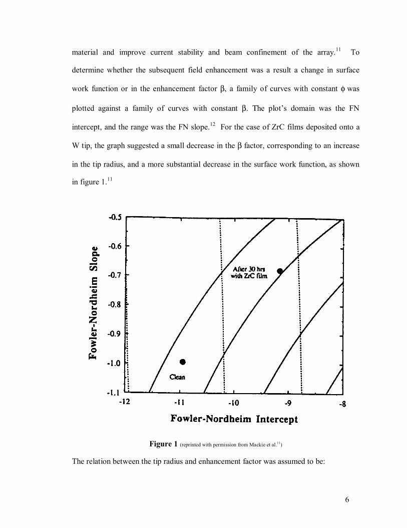
material and improve current stability and beam confinement of the array.11 To
determine whether the subsequent field enhancement was a result a change in surface
work function or in the enhancement factor β, a family of curves with constant φ was
plotted against a family of curves with constant β. Τhe plot’s domain was the FN
intercept, and the range was the FN slope.12 For the case of ZrC films deposited onto a
W tip, the graph suggested a small decrease in the β factor, corresponding to an increase
in the tip radius, and a more substantial decrease in the surface work function, as shown
in figure 1.11
Figure 1 (reprinted with permission from Mackie et al.11)
The relation between the tip radius and enhancement factor was assumed to be:

7
1
ln5.0−
=
rDrβ
where D is the tip to screen distance in an FEM tube.13
Then by assuming only a small increase in tip radius, the change in work function
due to deposition is given by the FN ratio:
32
=
clean
depositedFN m
mRatio
where m is the slope of the FN curve for the emitter before and after ZrC deposition.11
Using a similar procedure, Xie et al. were able to obtain a work function decrease of 0.6
eV after depositing ZrC on single crystal Si Spindt-type single emitters and a decrease on
the order of 1 eV for Mo polycrystalline wire. Again, the decrease in field enhancement
factor was sufficiently small to calculate FN ratios that corresponded with the change in
work function due to deposition.14
Carbides of hafnium, one period below Zr in group 4B, have been shown to have
lower work functions than ZrC by several tenths of an eV.15,12 Similarly, Mackie et al.13
have demonstrated that deposition of HfC films on W single tips, Mo single tips, and Mo
FEA's reduces surface work function below that of experiments with ZrC deposition on
the same substrates. In addition to the success of ZrC and HfC in lowering work
functions beyond those of uncoated tips, these carbides boast some of the highest melting
points of all materials and thus can maintain functionality at high temperatures and fields
without becoming subject to atom migration. ZrC and HfC usually exist in an fcc crystal
structure but are found with stoichiometries as low as (C/Zr) = 0.84. Nonetheless,
Mackie et al.16 have shown optimum current stability, optimal resistance to surface

8
contamination, and minimal noise levels with (C/Zr) = 1. Using x-ray photoelectron
spectroscopy (XPS) to measure carbon content of implanted silicon, Chen et al.17 found
the most preferable emission characteristics to come from the more stoichiometric films
also in the case of deposition of SiC on to an Si tip surface.
Tsang et al. also studied SiC deposition, characterized by high dose carbon
implants into silicon and showed that both surface morphology and electrical
inhomogeneities lent a hand in producing local electric field enhancement.18 Using
conducting atomic force microscopy (CAFM), he found localized graphitic clusters in
samples that were not annealed. Thermal annealing, however, produced a more uniform
SiC layer, destroying the clusters. Subsequent XPS experiments revealed the presence of
graphitic sp2 carbon in the as-implanted samples and its absence after annealing,
prompting the conclusion that electrical inhomogeneities were eliminated by complete
carbonization during the first hour of thermal annealing at 1200 °C. After longer
annealing times, small protrusion structures became detectable on AFM, leading to local
electric field enhancement.
In this work, plasma-sourced ion-implantation (PSII) of Group V transition metals
was performed to produce a thin carbon-implanted layer. In cases where implantation
yields a stable carbide, experimenters expected reductions in the work function beyond
that of the unimplanted metals, as seen in previous studies of other groups. In cases
where carbide formation is minimal or inexistent, the effect on field emission is entirely
unknown. Experimental work on the field emission enhancing properties of carbon
largely surpasses theoretical work, but several groups have put forth explanations on why
carbon implants and films enhance field emission.19,20 The fact that carbon has very low
or negative electron affinity -- and the conduction band lies close to or even above the

9
vacuum level -- makes it energetically favorable for an electron in that band to break
from the atom. Burden20 also suggests that the coexistence of carbon hybridized to sp2
and sp3 orbitals in the same region of a carbon-containing compound produces inclusions
and grain boundaries and hence regions of locally amplified electric field, thereby
making electron emission easier.

10
II. Theory
A. Fowler-Nordheim tunneling
Fowler and Nordheim first described the dependence of electron emission on a
high electric field as a simple barrier penetration situation, in which an incident electric
field so deforms a potential barrier that low-energy electrons may tunnel through the
classically forbidden region. The Heisenberg principle requires a correlation between
uncertainty in position and momentum of a surface electron. Supposing that an electron
near the surface of the material has a positional uncertainty on the order of the width of
the potential barrier, tunneling through the barrier is possible, as predicted by the
Wentzel-Kramers-Brillouin (WKB) method for one-dimensional potentials. The current
is predicted as:
( ) ( ) ( )∫ +−=eV
ts dEreVETEeVrErI0
,,,, ρρ ,

11
where ρs and ρt are the density of states of the sample and tip, respectively, eV is the
sample bias, E is the electron energy, r is located directly under the tip, and T is the
transmission probability, given by:
( )
−+
+−= EeVmzeVET ts
2222exp,
φφh
,
for work functions φ and tip-sample distance z. 21
In the case of an incident electric field on a one-dimensional metallic surface, the
WKB method describes a triangular potential. Multiplying the WKB probability by the
differential rate of electron arrival at the surface, and integrating the electron kinetic
energy from zero to the Fermi level, Fowler and Nordheim arrived at an expression for
current density, valid for an instantaneous potential barrier.7
Figure 2 (reprinted from Gomer7)
12
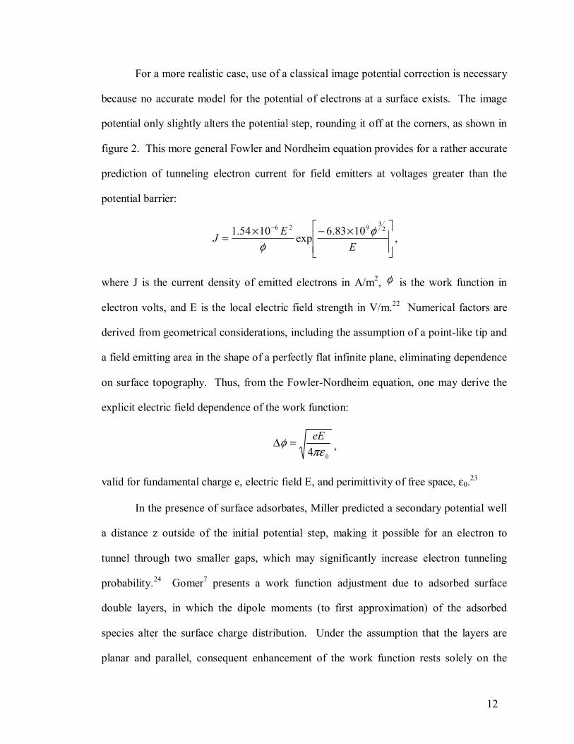
For a more realistic case, use of a classical image potential correction is necessary
because no accurate model for the potential of electrons at a surface exists. The image
potential only slightly alters the potential step, rounding it off at the corners, as shown in
figure 2. This more general Fowler and Nordheim equation provides for a rather accurate
prediction of tunneling electron current for field emitters at voltages greater than the
potential barrier:
×−×=−
EEJ
23926 1083.6exp1054.1 φ
φ,
where J is the current density of emitted electrons in A/m2, φ is the work function in
electron volts, and E is the local electric field strength in V/m.22 Numerical factors are
derived from geometrical considerations, including the assumption of a point-like tip and
a field emitting area in the shape of a perfectly flat infinite plane, eliminating dependence
on surface topography. Thus, from the Fowler-Nordheim equation, one may derive the
explicit electric field dependence of the work function:
04πεφ eE=∆ ,
valid for fundamental charge e, electric field E, and perimittivity of free space, ε0.23
In the presence of surface adsorbates, Miller predicted a secondary potential well
a distance z outside of the initial potential step, making it possible for an electron to
tunnel through two smaller gaps, which may significantly increase electron tunneling
probability.24 Gomer7 presents a work function adjustment due to adsorbed surface
double layers, in which the dipole moments (to first approximation) of the adsorbed
species alter the surface charge distribution. Under the assumption that the layers are
planar and parallel, consequent enhancement of the work function rests solely on the

13
number of dipoles and their strengths, aside from a solid angle factor of 4π. Plausibly
assuming the dipole is centered on the electrical midpoint in the double layer, such that
an electron need only do work against half of the layer, Gomer concludes:
θπφ si NP2=∆ ,
where Pi is the dipole moment of an adsorbed particle, Ns is the total number of
adsorption sites per unit area, and θ is the fraction of filled sites.7 The surface dipole
assumption is also valid for surfaces without adsorbed layers and is likewise dependent
on the number of dipole sites. More loosely packed surfaces lead to atomic scale
corrugations on the surface and the subsequent formation of dipoles oriented in the
opposite direction of the surface dipole, as seen in figure 3. The result of this
phenomenon, known as the Smoluchowski effect, is an overall lowering of the
macroscopic work function.25
Figure 3 (reprinted from Hasegawa et al.26)

14
B. Plasma Source Ion Implantation
During the PSII, the target to be implanted is submerged in an ionized plasma and
is then pulsed with a high negative voltage, in this case -35 kV at 25 Hz. The target and
mount are electrically isolated from the chamber walls by a quartz rod. The pulse repels
free electrons throughout the plasma while attracting the ions, which are subsequently
implanted into the surface of the target. Anders 26 presents a planar model of a sheath,
assuming collisionless ion flow, zero electron mass, an instantaneous voltage pulse, the
instantaneous formation of the ion sheath, singly charged ions, and that the implant
current wholly provides the charge of the expanding sheath. By equating the current
density as derived by Child’s law to the charge per unit time crossing the boundary of the
ion sheath, Anders arrives at the sheath velocity:
20
20
92
sus
dtds = ,
for
21
0
000
2
=
enV
sε
and MeV
u 00
2=
where, s is the sheath position, s0 is the thickness of the ion matrix sheath, ε0 is the
permittivity of free space, V0 is the pulse voltage, e is the fundamental charge, and M is
the ion mass. 27 Analytically integrating the differential equation produces
[ ] 31
0 132 += tss piω ,
where ωpi is the ion plasma frequency.28 Assuming that the target current is only
supplied by ionization during sheath expansion, this solution allows us the average ion
current per pulse as
15
fpulse
ion stenAI
= ,
with sf the final sheath extent as calculated by the above analytical solution to the sheath
velocity differential equation.25
For a low-pressure plasma at high pulse voltage and small pulse-width, these
assumptions are good approximations. The plasma in this work, however, consists of
multiple ions of different masses and charges. The sheath velocity of a plasma of this
consistency must be modified by replacing the ion mass with an effective mass, given by:
∑=j
jjj MZkM
with Zj and Mj signifying atomic number and mass for each ion j and kj defined as the
fractional density of ion j as follows: 24
∑=
Z z
jj Zn
nk .
As the voltage pulse continues, the sheath of ions expands radially outward from
the pulsed sample. When the pulse ends, however, the sheath collapses as the charge
from the sample and holder is discharged through the electronics, and the neutralized
target is again ready for the next pulse. The plasma, on the other hand, may still be
nonuniform by the time of the next pulse, depending on repetition rate and sheath
thickness. This situation causes the next pulse to expand the ion sheath further, and if left
unchecked, creates the possibility of arcing with the chamber walls on subsequent pulses.
This effect is more pronounced in low density plasmas because of the wide sheath
produced with a single pulse. Anders 26 is quick to point out that the pulse expansion
does eventually reach a steady state in much less time than is required for the total
implant.

16
PSII is a low-temperature surface processing technique that causes minimal
thermal distortion of the sample with no macroscopic change in dimensions and produces
no degradation in the surface finish.29 Between pulses, the target to be implanted loses
heat energy by radiation and conductive contact with the sample stage. The temperature
of the implant is determined by four major factors: heating by the pulses, heat loss
through conduction with the stage, radiation loss, and convection with the implant
plasma. Thus, the time dependence of the temperature is given by:
( ) ( )q
bqqp L
TTAKTTAAq
dtdTmc
−−−−= 4
04εσ ,
where A is the target’s surface area, q is the time-average heat from the pulses, ε is the
emissivity of the target surface, T0 is the temperature of the plasma, Kq is the thermal
conductivity of the quartz rod that holds the sample stage, Aq is the cross-sectional area
of the rod, Lq is its length, and Tb is the temperature of the bottom wall of the chamber,
with which the rod is in contact. Heat loss by radiation from the rod is assumed to be
minimal and may be ignored.27
After the implantation procedure, electrical activation of doped materials, usually
done by high-temperature annealing, is necessary to increase the substitutional fraction of
the dopant species and to repair the crystal lattice damage due to the implantation process
that otherwise would degrade the electrical properties of the material. The samples in
this work, however, were not annealed so as to maintain the high-aspect surface features
and electrical inhomogeneities that are crucial to localize high-density electric fields and
hence electron emission at low temperatures. The surface of a crystalline solid does not
exhibit the three-dimensional periodicity of the bulk material, and surface atoms relax to
eliminate dangling bonds.30 A common example is the (001) face of silicon, in which
17
structure relaxation results in the formation of Si-Si dimers. In compound
semiconductors, charge transfer between dangling bonds on cations and anions produces
local regions of high electric field, which may enhance field emission characteristics.
C. X-ray Photoelectron Spectroscopy
Siegbahn et al.30 were the first to use the high-resolution energy spectra of x-ray
stimulated electrons to study atomic energy orbitals. This technique, known as X-ray
Photoelectron Spectroscopy (XPS) or Electron Spectroscopy for Chemical Analysis
(ESCA), uses soft x-ray photons -- often from MgKα -- to prompt electron emission from
a target material.31 All electrons with binding energy Eb < hν may be excited by incident
x-rays, but the probability for certain emissions is higher, producing sharp peaks in the
energy spectrum. If the electron kinetic energy is measured by a detector, the binding
energy is calculated as:
sKEhEb φν +−= ,
where φs is the work function of the detector, which must be calibrated.32 The effective
sample depth measured by XPS is based on the electron mean free path (MFP) and is a
function of both sample composition and electron kinetic energy and thus in general is
not constant throughout the spectrum. As a rule of thumb penetration depth is limited to
5-20 Å in base metals and 15-40 Å in oxides but can reach as deep as 40-100 Å in
polymeric materials. In the case of metals, the minimum depth measurement occurs
around electron energies of 50 eV and increases linearly to first approximation at higher
energies, reaching 20 Å near 2000 eV, as shown in figure 4.32 Relative intensities of the
photo-peaks may be used to calculate abundance ratios of elements within the material.
A complete analysis would involve MFP variations due to crystallographic structure and

18
electron kinetic energy, but a simpler analysis can be performed by simply dividing
relative peak heights by the photoelectric cross-sections of the element. Photoelectric
cross sections for the C1s level for different elements when subjected to MgKα can be
found in reference 32.
Figure 4 (reprinted from Riggs and Parker32)
A depth distribution of the form
( ) ( )[ ]2exp eqzzbbzP −−=π
is expected, for distance from surface z, and a Gaussian distribution centered at an
equilibrium distance zeq and of width b
1 .33
D. Scanning Tunneling Microscopy
The theory of STM tunneling current was first described with perturbation theory
by Bardeen in 1961. 34 In the limit of small bias voltage and a relatively large sample-tip

19
distance, the perturbation technique provides a sufficient analysis of the tunneling
mechanism for a single-atom STM tip.
Figure 5: (reprinted from Stroscio and Feenstra35)
Stroscio and Feenstra35 calculate the tunneling current between two free electron
metals for the planar energy barrier illustrated in figure 5 as:
( ) ( )∫∞
=0
zzz ENEDdEj
in which Ez is the energy component normal to the metal surfaces. The normal energy
distribution is given by:
( ) ( ) ( )[ ]∫ +−= parallelz dEeVEfEfhmeEN 3
4π ,

20
where f(E) is the Fermi-Dirac distribution function, and the transmission probability is
approximated by:
( ) ( )sED z κ2exp −≈ ,
which holds for small voltages and energies near the Fermi level. In this equation, s is
the tip-sample spacing, and κ is the vacuum decay constant:
2
2h
φκ m=
By examination of the exponential dependence of the tunneling probability on tip-sample
distance, Sasaki and Tsukada point out that in the case of a small protrusion in the sample
surface, almost all tunneling current originates from that area.36
Assuming the tip is a mathematical point source of current, Tersoff treats STM
tunneling as a first-order perturbation situation and arrives at:
),( eVEdVdI
F −∝ Rρ
where ρ gives the local density of states (LDOS) at the surface of the protrusion,
assuming that the LDOS of the tip is smooth relative to that of the surface, or else higher-
order derivatives will play a measurable role.37 In this case, a more complete theoretical
simulation is necessary; one can be found in van Loenen et al., but it is well beyond the
scope of this paper.38 Stroscio avoided this problem by plotting the ratio of differential to
total conductivity measurements as a function of energy, thereby removing the
dependence of the tunneling current on the voltage gap and separation distance and
obtaining relatively direct measurement of the LDOS. Then, to ensure that the plot
contained no LDOS features of a tungsten probe tip, they scanned both silicon surfaces

21
and nickel films and finding no common peaks, concluded that tungsten probe tips
contribute no significant features to the spectra.39
In any case, the dynamic inductance (dI/dV) can be measured using STM in
spectroscopy mode by holding the tip-sample distance constant and varying the bias
voltage over a single point on the surface of the sample. I(V) characteristics may be
compared to a modified form of the FN equation:
VeVeAI βφ
φ βφ
23
72
1 1053.62286.96 1104.1
×−− −
×=
for current I and emitting area A and where β is the field enhancement factor.12 For
smooth emitters with tip to sample distance of less than about one micron, β may be
expressed under a hyperbolic model as a function of the tip radius:
=
tt
H
rRr 4ln
2β ,
where rt is the tip radius and R is the tip-sample distance.40
In current vs. distance plots in STS of metal surfaces, an exponential dependence
of tunneling current on the tip-sample separation is well known. Kuk plots tunneling
current as a function of gap distance on semi-logarithmic axes, obtaining the work
function as:
2ln952.0
=
dSIdφ ,
for a Na single-atom tip, where S is the tip-sample separation.41 This equation holds only
for local barrier heights (LBH’s) when the tip-sample distance is greater than ~5 Å,
where the barrier can be treated as a small perturbation between two independent metallic
states, corresponding to the tip and the sample surface. For closer distance, the

22
perturbation term becomes larger, and the slope may vary over this region.
Unfortunately, the size and shape of the probe tip and the detailed topology of the sample
surface play a large role in measuring the barrier height. Kuk also presents a more
reliable measure of work function for gap voltages below the work function, where
tunneling current is not described by the Fowler-Nordheim equation but depends
exponentially on the work function: 40
φ05.1−≈ VeI ,
where φ is in eV.
Citing Tersoff-Hamann theory, Hamers and Padowitz also give an equation for
current that is linear in voltage for small gap biases, about 10 mV:
( ) ( )VErDEDeReI FsFtR ,32 0
2422213 κκφπ −−= h ,
where R is the tip radius, Dt is the tip density of states at the Fermi level, Ds is the surface
density of states at the Fermi level directly under the tip, and κ is the vacuum decay
constant.21
23
III. Experimental Procedure:
Square foils (7 mm x 7 mm) of Group V transition metals – 99.8% vanadium,
99.98% niobium, and 99.95% tantalum – were implanted with carbon ions at ~35 kV for
seven hours at a pulse rate of 125 Hz. The vanadium foil was 0.127 mm thick, the
niobium was 1.0 mm, and the tantalum was 0.5 mm. The implantation chamber was
pumped down by a CIT-Alcatel Type 2033 mechanical pump and a Seiko Seiki STPH-
1000 turbo-maglev, backed by an Edwards GVSP 30A scroll pump, all of which were dry
pumps. Pump speed was throttled by an iris valve. The implant plasma was held at a
pressure of 2.4 x 10⁻³ Torr and was composed of 2% methane gas with a mixture of 4%
hydrogen and 94% argon to minimize carburization on the walls of the implantation
chamber. Use of methane (CH4) as carbon source, however, decreased carbon
implantation energies by a factor of 25% because the total mass of a methane molecule,
16 amu, derives only 12 amu of that mass from carbon. Therefore during a 35 kV
implantation, carbon ions implanted at only 26.25 kV. The plasma was driven by an RF
power supply capable of an output of 2.00 kW and operated at 850 W at 13.6 MHz
24
through three variable capacitors to allow for fine tuning to match the impedance load of
the power supply to that of the plasma. It was inductively coupled to the chamber,
providing a higher plasma density than a capacitively coupled arrangement would have,
and thus allowing a greater ion flux per pulse as well as a longer pulse length without
danger of the ion sheath extending to the wall, minimizing the possibility of arcing and
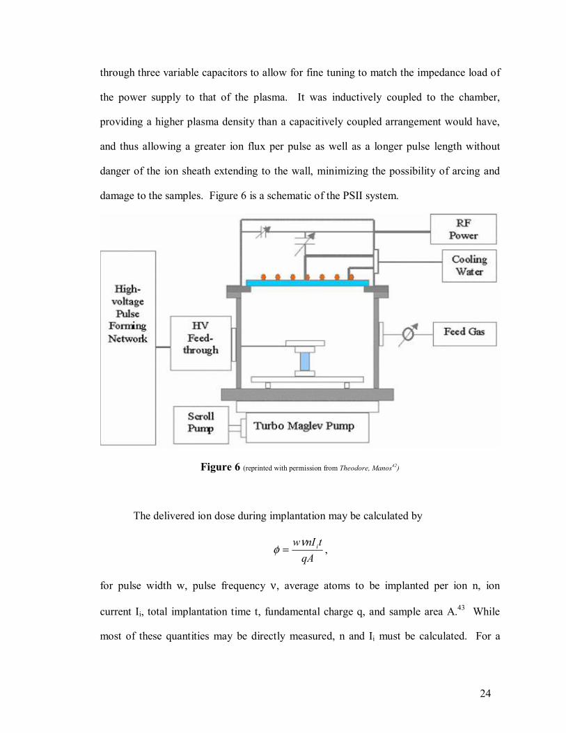
damage to the samples. Figure 6 is a schematic of the PSII system.
Figure 6 (reprinted with permission from Theodore, Manos42)
The delivered ion dose during implantation may be calculated by
qAtnIw iνφ = ,
for pulse width w, pulse frequency ν, average atoms to be implanted per ion n, ion
current Ii, total implantation time t, fundamental charge q, and sample area A.43 While
most of these quantities may be directly measured, n and Ii must be calculated. For a

25
methane plasma, the relative concentrations of CH3+ and CH4
+ are difficult to determine
experimentally. Fortunately, in each case ncarbon = 1, and no calculation is necessary.
Calculating ion current, however, is more involved but was done by our group43, giving:
γ+−
=1
dti
III ,
where It is the total current as measured by an ammeter at the output of the transformer, Id
is the displacement current, which can be measured by pulsing the sample with no plasma
in the chamber, and γ is the secondary electron emission coefficient. By substitution, the
dose rate may be calculated as:
( )( )γ
νφ+−
=1qA
IIntw dt .
Previous experimentation with this chamber allowed samples to be placed in a
region of highly uniform plasma density.27 High negative voltage pulses were created by
a pulse-forming network (PFN) in which a thyratron, driven by the generated pulse,
determined the pulse rate by grounding out for a certain time, thereby triggering a 10X
step-up transformer. The PFN was capable of producing 100 kV, 30 A pulses at 200 Hz.
A network of capacitors and inductors removed “ripple” from the pulse shape in order to
achieve a more uniform voltage. After implantation, the samples underwent no
annealing. For comparison, similar samples of vanadium, niobium, and tantalum metals
were cut and examined without being submitted to carbon implantation.
XPS measurements were carried out on the implanted and bare metals to
determine whether carbides were formed during implantation. The preparation chamber
of the XPS system was pumped down to 10-2 Torr with a roughing pump, followed by a
turbo molecular pump and a diffusion pump, which decreased the pressure to 10-8 Torr.
After movement to the analysis chamber, an ion pump dropped the pressure to ≤ 10-9

26
Torr. For analysis, a twin anode MgKα source was used to produce an emission current
of 10 mA at 10 kV for a power output of 200 W. The detector was a channeltron, a three-
centimeter-long horn-shaped continuous photomultiplier. The channel was made of
evacuated, semiconductive glass. When an incident electron strikes this surface, it expels
more electrons, which are then accelerated towards the anode, hitting the walls several
more times and each time generating more secondary electrons.44 Figure 7 is a
photograph of the XPS system. The bulbous top-most portion is the hemispherical mirror
analyzer with the channeltron located in an appendage in the foreground below. The
window under it looks into the analysis chamber, and the preparation chamber sticks out
on the right side.
Figure 7
27
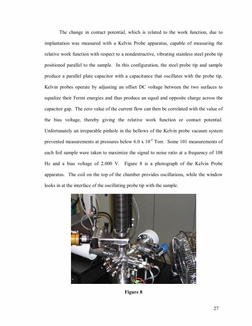
The change in contact potential, which is related to the work function, due to
implantation was measured with a Kelvin Probe apparatus, capable of measuring the
relative work function with respect to a nondestructive, vibrating stainless steel probe tip
positioned parallel to the sample. In this configuration, the steel probe tip and sample
produce a parallel plate capacitor with a capacitance that oscillates with the probe tip.
Kelvin probes operate by adjusting an offset DC voltage between the two surfaces to
equalize their Fermi energies and thus produce an equal and opposite charge across the
capacitor gap. The zero value of the current flow can then be correlated with the value of
the bias voltage, thereby giving the relative work function or contact potential.
Unfortunately an irreparable pinhole in the bellows of the Kelvin probe vacuum system
prevented measurements at pressures below 6.0 x 10⁻² Torr. Some 101 measurements of
each foil sample were taken to maximize the signal to noise ratio at a frequency of 108
Hz and a bias voltage of 2.000 V. Figure 8 is a photograph of the Kelvin Probe
apparatus. The coil on the top of the chamber provides oscillations, while the window
looks in at the interface of the oscillating probe tip with the sample.
Figure 8
28
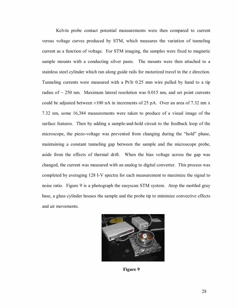
Kelvin probe contact potential measurements were then compared to current
versus voltage curves produced by STM, which measures the variation of tunneling
current as a function of voltage. For STM imaging, the samples were fixed to magnetic
sample mounts with a conducting silver paste. The mounts were then attached to a
stainless steel cylinder which ran along guide rails for motorized travel in the z direction.
Tunneling currents were measured with a Pt/Ir 0.25 mm wire pulled by hand to a tip
radius of ~ 250 nm. Maximum lateral resolution was 0.015 nm, and set point currents
could be adjusted between ±100 nA in increments of 25 pA. Over an area of 7.32 nm x
7.32 nm, some 16,384 measurements were taken to produce of a visual image of the
surface features. Then by adding a sample-and-hold circuit to the feedback loop of the
microscope, the piezo-voltage was prevented from changing during the “hold” phase,
maintaining a constant tunneling gap between the sample and the microscope probe,
aside from the effects of thermal drift. When the bias voltage across the gap was
changed, the current was measured with an analog to digital converter. This process was
completed by averaging 128 I-V spectra for each measurement to maximize the signal to
noise ratio. Figure 9 is a photograph the easyscan STM system. Atop the mottled gray
base, a glass cylinder houses the sample and the probe tip to minimize convective effects
and air movements.
Figure 9
29
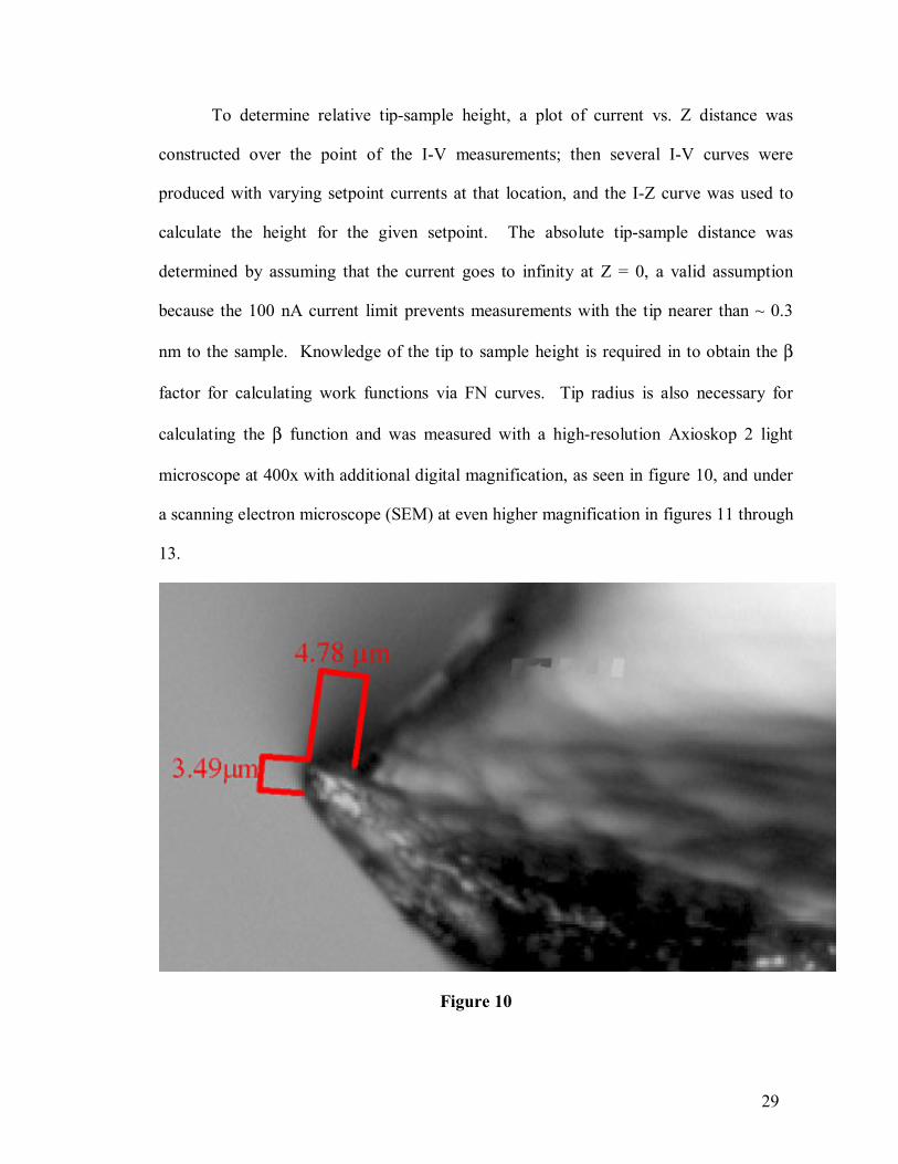
To determine relative tip-sample height, a plot of current vs. Z distance was
constructed over the point of the I-V measurements; then several I-V curves were
produced with varying setpoint currents at that location, and the I-Z curve was used to
calculate the height for the given setpoint. The absolute tip-sample distance was
determined by assuming that the current goes to infinity at Z = 0, a valid assumption
because the 100 nA current limit prevents measurements with the tip nearer than ~ 0.3
nm to the sample. Knowledge of the tip to sample height is required in to obtain the β
factor for calculating work functions via FN curves. Tip radius is also necessary for
calculating the β function and was measured with a high-resolution Axioskop 2 light
microscope at 400x with additional digital magnification, as seen in figure 10, and under
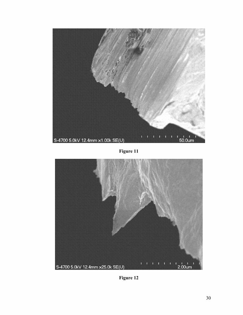
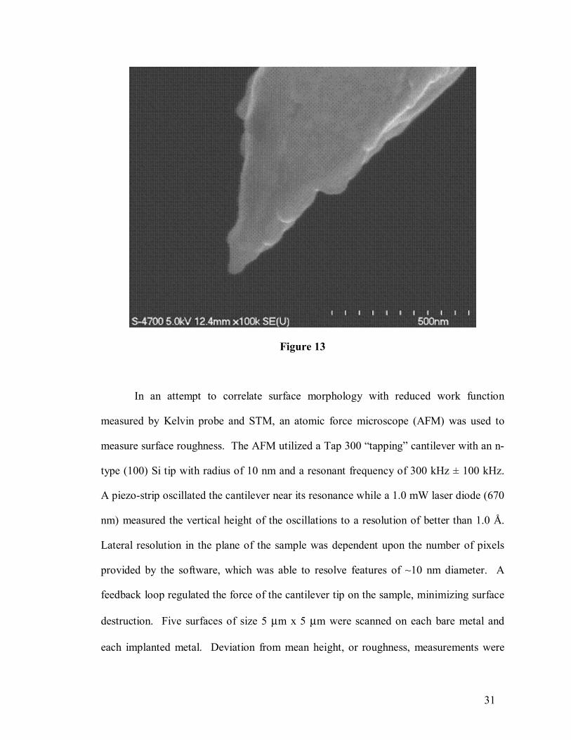
a scanning electron microscope (SEM) at even higher magnification in figures 11 through
13.
Figure 10
30
Figure 11
Figure 12
31
Figure 13
In an attempt to correlate surface morphology with reduced work function
measured by Kelvin probe and STM, an atomic force microscope (AFM) was used to
measure surface roughness. The AFM utilized a Tap 300 “tapping” cantilever with an n-
type (100) Si tip with radius of 10 nm and a resonant frequency of 300 kHz ± 100 kHz.
A piezo-strip oscillated the cantilever near its resonance while a 1.0 mW laser diode (670
nm) measured the vertical height of the oscillations to a resolution of better than 1.0 Å.
Lateral resolution in the plane of the sample was dependent upon the number of pixels
provided by the software, which was able to resolve features of ~10 nm diameter. A
feedback loop regulated the force of the cantilever tip on the sample, minimizing surface
destruction. Five surfaces of size 5 µm x 5 µm were scanned on each bare metal and
each implanted metal. Deviation from mean height, or roughness, measurements were

32
calculated by arithmetic averaging, Ra, and the root mean squared method, Rq, over the
scanned areas. A photograph of the AFM appears in figure 14. The samples were
mounted on the silver disk and rotated to a position under the cantilever, which is located
directly under the matte silver laser housing. The optics also point to this location.
Figure 14

33
IV. Data Analysis
A. STM Data
STM imaging was used to evaluate topographically smooth locations for
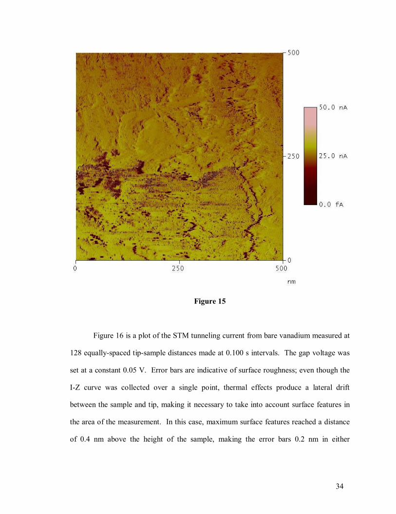
obtaining I-V and I-Z curves. Figure 15 is a map of tunneling current taken at constant
height across an area of 500 nm x 500 nm. The procedure for obtaining stable I-V
curves in small areas was to scan a large sample size, choose the smoothest area -- in this
case perhaps in the upper left-hand corner, and then zoom in to choose the smoothest area
again. This technique minimized the role large-scale (greater than a few nanometers)
surface features had in effecting work function measurements.
34
Figure 15
Figure 16 is a plot of the STM tunneling current from bare vanadium measured at
128 equally-spaced tip-sample distances made at 0.100 s intervals. The gap voltage was
set at a constant 0.05 V. Error bars are indicative of surface roughness; even though the
I-Z curve was collected over a single point, thermal effects produce a lateral drift
between the sample and tip, making it necessary to take into account surface features in
the area of the measurement. In this case, maximum surface features reached a distance
of 0.4 nm above the height of the sample, making the error bars 0.2 nm in either
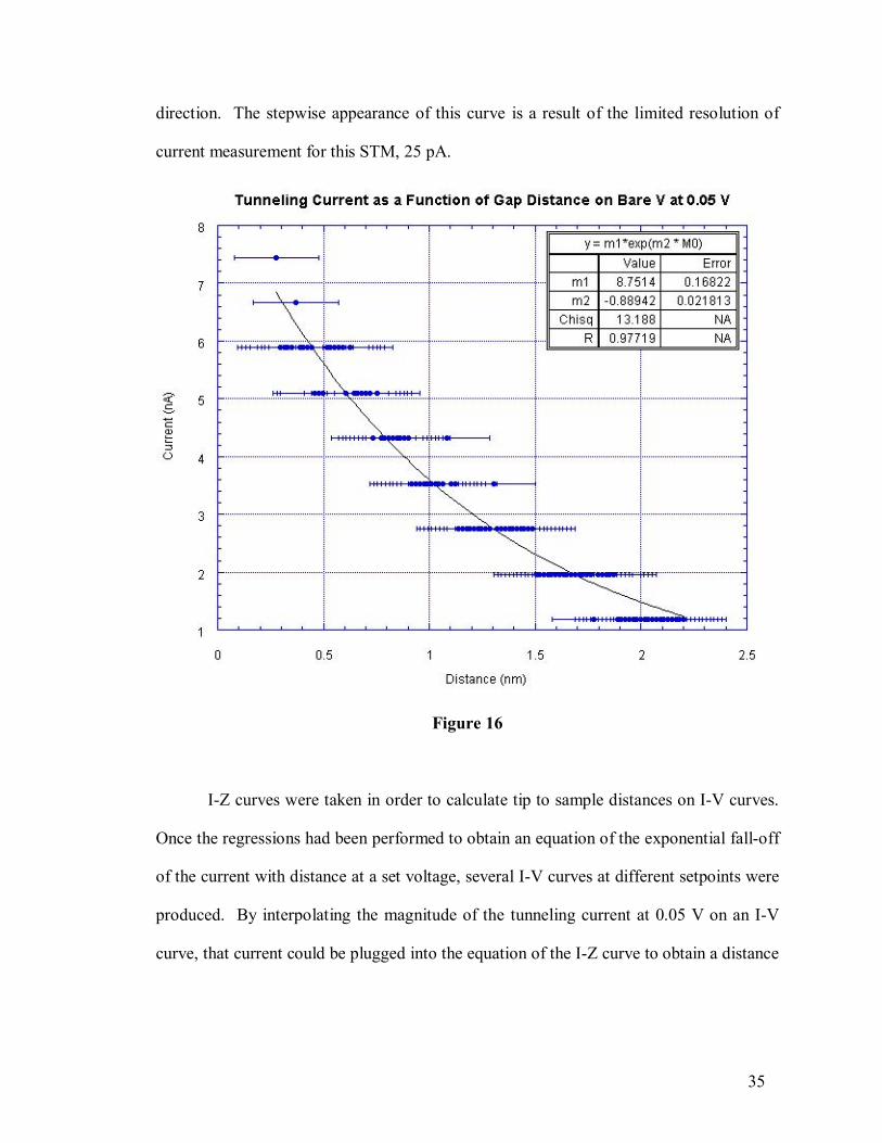
35
direction. The stepwise appearance of this curve is a result of the limited resolution of
current measurement for this STM, 25 pA.
Figure 16
I-Z curves were taken in order to calculate tip to sample distances on I-V curves.
Once the regressions had been performed to obtain an equation of the exponential fall-off
of the current with distance at a set voltage, several I-V curves at different setpoints were
produced. By interpolating the magnitude of the tunneling current at 0.05 V on an I-V
curve, that current could be plugged into the equation of the I-Z curve to obtain a distance

36
for that particular I-V spectrum. This procedure could be completed with the following
formula:
=
AVF
BZ )(ln1 ,
where A and B are constants given by the exponentials for I-V and I-Z curves, as follows:
( )BzAi exp=
for current i, voltage V, and separation z, and where F(V) is linear in V for small voltages
(less than ~ 10 mV) and becomes exponential at higher gap biases.21,40 Such I-Z curves
were measured twice for each metal, once on the bare specimen and once on the carbon-
implanted metal. Each is similar in shape to that of bare vanadium and is closely mapped
by an exponential decline, as expected theoretically. These I-Z curves appear in
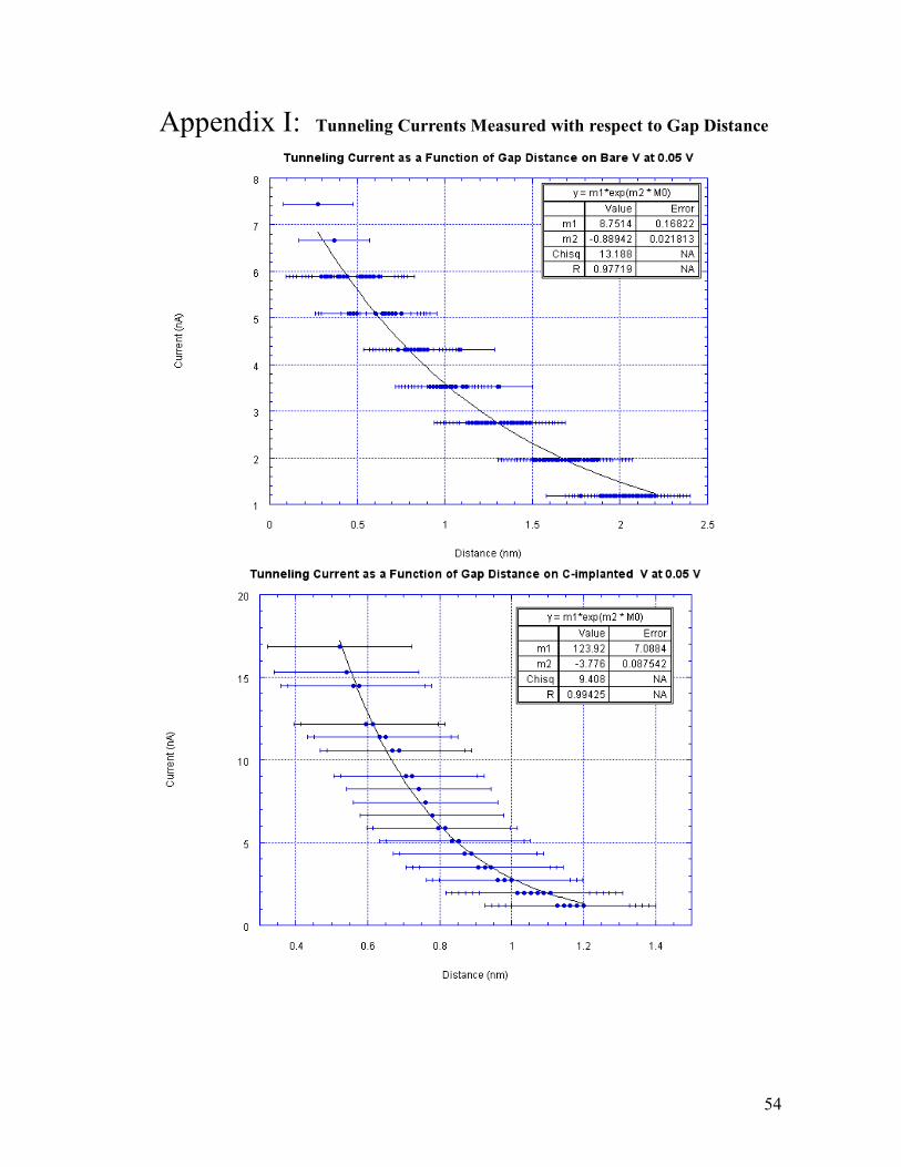
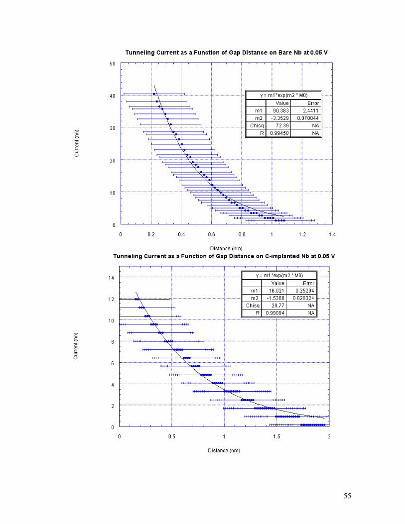
Appendix I: “Tunneling Currents Measured with respect to Gap Distance.”
Figure 17 is an overlay of I-V curves of bare vanadium taken at increasing tip-
sample separations. As is well known, measurements taken a greater distance away from
the sample require exponentially higher voltages before they become significant current
sources.

37
Figure 17
For voltages greater than ~ 0.4 V, curves are neatly approximated by exponentials of the
form:
( )bVai exp= ,
for constant a and b.
As the tip-sample distance closes, however, the curves become increasingly more
linear and are better fit by equations of the form:
( )bVaVi exp= ,
and thus contain a linear and exponential portion. Although the researcher did not reach
currents low enough to see completely linear behavior on bare vanadium, he was able to
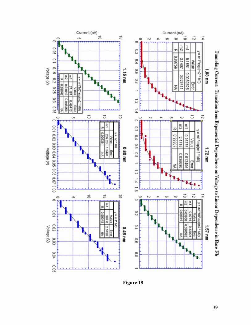
do so on bare niobium and tantalum samples. Figure 18 contains six plots of tunneling

38
current against voltage on bare niobium, taken at different tip-sample separations with the
intent of making the linearization transition more visible. In the data sets that are best fit
by pure exponentials, the points are colored red, those best fit by straight lines are colored
blue, and those best fit by a multiplicative hybrid are green. Curve fit R values are above
0.993 for all regressions, despite the stepwise appearance of the curves due to limited
current resolution. Numerically, one may see the linearization trend as an increase in the
scaling parameter a (or m1) and a decrease in the exponential parameter b (or m2) as
defined in the equation:
( )bVaVi exp=
Note that the exponential approaches unity as (bV) becomes smaller, and voltages in this
region are usually one to two orders of magnitude below unity. Overlays of I-V curves of
unimplanted and implanted samples of each metal are available in Appendix II:
“Tunneling Currents Measured with respect to Bias Voltage.” The researcher has been
unable to explain a distance-scaling error of ~ 4 in the plot of bare Ta. It is likely that an
error was made with a setting during data collection.
39
Figure 18

40
In the case of voltages greater than the work function, it is possible to calculate
the barrier potential using the Fowler-Nordheim method:
VeVeAI βφ
φ βφ
23
72
1 1053.62286.96 1104.1
×−− −
×=
for emitting area A and field enhancement factor β.12 Traditionally, this procedure is
done by plotting
2lnVI against
V1 , from which a straight line is obtained with slope:
βφ 2
371053.6 ×=m
and intercept:
×=
−
−
φβ
φ 21
86.9261040.1ln eAb 45
In the case of this work, however, the 100 nA limit on the STM required voltages to
remain well below the work function, and attempts to produce an FN plot resulted in
logarithmic curves, such as Figure 19. On the high voltage end of this plot, it appears as
though the behavior may be approaching linearity, but current limit prevents any further
progression. The discontinuities at the high-voltage end (small values of 1/V) are a
product of current overloads causing the STM software to abort measurements and to
average values of zero at that location for some of the 128 measurements that were taken.

41
Figure 19
For lower voltages, however, Kuk presents another method of calculating the
approximate work function, as follows:
φ05.1−≈ VeI ,
where the constant has been adjusted so that the voltage is measured in volts, the current
in nanoamps, and the work function in electron volts.40 By this method, Table 1 is
calculated. Accepted values for bare materials are 4.3 eV for vanadium and niobium and
4.25 eV for tantalum.46 Error values listed in this table arise only from discrepancies
with the curve fitting. Additional errors – most notably thermal drift – have not been
accounted for. Deviations from the accepted value may be an effect of the thermal drift,
or may be a result of any contradictions with Kuk assumptions. It is worthy to note that

42
vanadium foils used in this experiment were by far the most reflective and the least
rough, characteristics necessary for STM. Niobium foils in particular were visibly more
“matte” than vanadium and contained large-scale (~ 1-2 µm) surface features. Kuk’s
paper provides no detailed justification for this linear approximation, nor does he detail
under what circumstances it holds. It appears, however, to be appropriate for the cases
we analyzed.
Work Functions, Calculated by Kuk Linear Approximation
Material Work Function Bare V 4.33 ± 0.03 eV C-imp V 4.28 ± 0.03 eV Bare Nb 5.22 ± 0.01 eV C-imp Nb 4.71 ± 0.01 eV Bare Ta 4.45 ± 0.01 eV C-imp Ta 4.48 ± 0.01 eV
Table 1
Figure 20 is a comparison of graphs of DOS measurements of bare and implanted
vanadium, niobium, and tantalum measured at a tip-sample distance of about 2 nm. The
noise on the low voltage end is due again to finite current resolution but in this case is
magnified as a derivative over a discontinuous region. For most of these plots, any
changes due to implantation are obscured by the noise. Qualitatively, it may be possible
to discern a slightly lower increase in the density of states with voltage after implantation,
but with such a low signal-noise ratio, it is impossible to say without better
measurements.

43
Figure 20
44
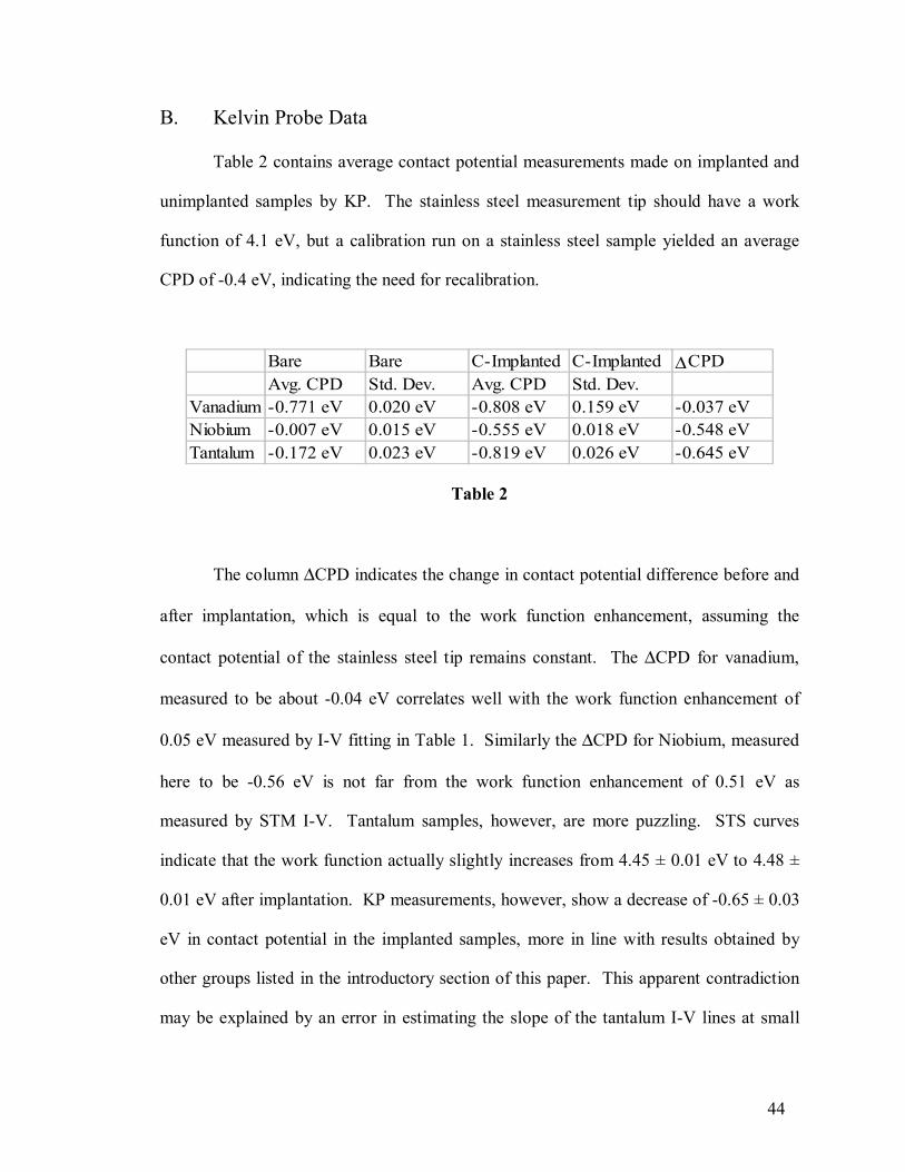
B. Kelvin Probe Data
Table 2 contains average contact potential measurements made on implanted and
unimplanted samples by KP. The stainless steel measurement tip should have a work
function of 4.1 eV, but a calibration run on a stainless steel sample yielded an average
CPD of -0.4 eV, indicating the need for recalibration.
Bare Bare C-Implanted C-Implanted ∆CPDAvg. CPD Std. Dev. Avg. CPD Std. Dev.
Vanadium -0.771 eV 0.020 eV -0.808 eV 0.159 eV -0.037 eVNiobium -0.007 eV 0.015 eV -0.555 eV 0.018 eV -0.548 eVTantalum -0.172 eV 0.023 eV -0.819 eV 0.026 eV -0.645 eV
Table 2
The column ∆CPD indicates the change in contact potential difference before and
after implantation, which is equal to the work function enhancement, assuming the
contact potential of the stainless steel tip remains constant. The ∆CPD for vanadium,
measured to be about -0.04 eV correlates well with the work function enhancement of
0.05 eV measured by I-V fitting in Table 1. Similarly the ∆CPD for Niobium, measured
here to be -0.56 eV is not far from the work function enhancement of 0.51 eV as
measured by STM I-V. Tantalum samples, however, are more puzzling. STS curves
indicate that the work function actually slightly increases from 4.45 ± 0.01 eV to 4.48 ±
0.01 eV after implantation. KP measurements, however, show a decrease of -0.65 ± 0.03
eV in contact potential in the implanted samples, more in line with results obtained by
other groups listed in the introductory section of this paper. This apparent contradiction
may be explained by an error in estimating the slope of the tantalum I-V lines at small

45
tip-sample separations due to too few measurements. At small tip-sample distances,
electron emissions from both bare and implanted tantalum quickly reach values above the
STM current limit, and the measurements cannot be used.
C. XPS Data
Figure 21
Figure 21 is a comparison of scans of the carbon C1s peak in bare V and C-
implanted V. In the unimplanted plot, the high-energy shoulder of the peak is
characteristic of carbon peaks in metals. In the implanted plot, a shoulder at a lower
binding energy (BE) has appeared, indicating a C-metal bond and the formation of a
carbide. Fujihana et al. specified binding energies for C-O bonds to be 281.6 eV, C-C
bonds as 284.2 eV, and C-metal bonds to range from 281.0 eV to 283.3 eV for transition
metal carbides.47 A constant shift of ~7 eV from book values indicates that the XPS
needs to be recalibrated. Because peak height is proportional to the implanted
concentration, only a proportionally small amount of carbide was formed.

46
Figure 22
Figure 22 is a comparison of scans of the V2p metal peak in bare and implanted
vanadium. Two metal peaks are visible in the bare spectrum: a sharp peak at 523 eV,
corresponding to the 2p3/2 state; a lower peak at 531 eV, the 2p1/2 state; and the O1s peak
is just visible at 536 eV.48 In the implanted spectrum, a third peak has appeared at higher
BE than the 2p3/2 state, as has a high BE shoulder developed on the 2p1/2 state. These
peaks provide further evidence of either carbon or oxygen, and likely both, bonding to the
metal as mixed oxides and carbides.49
Figure 23
47
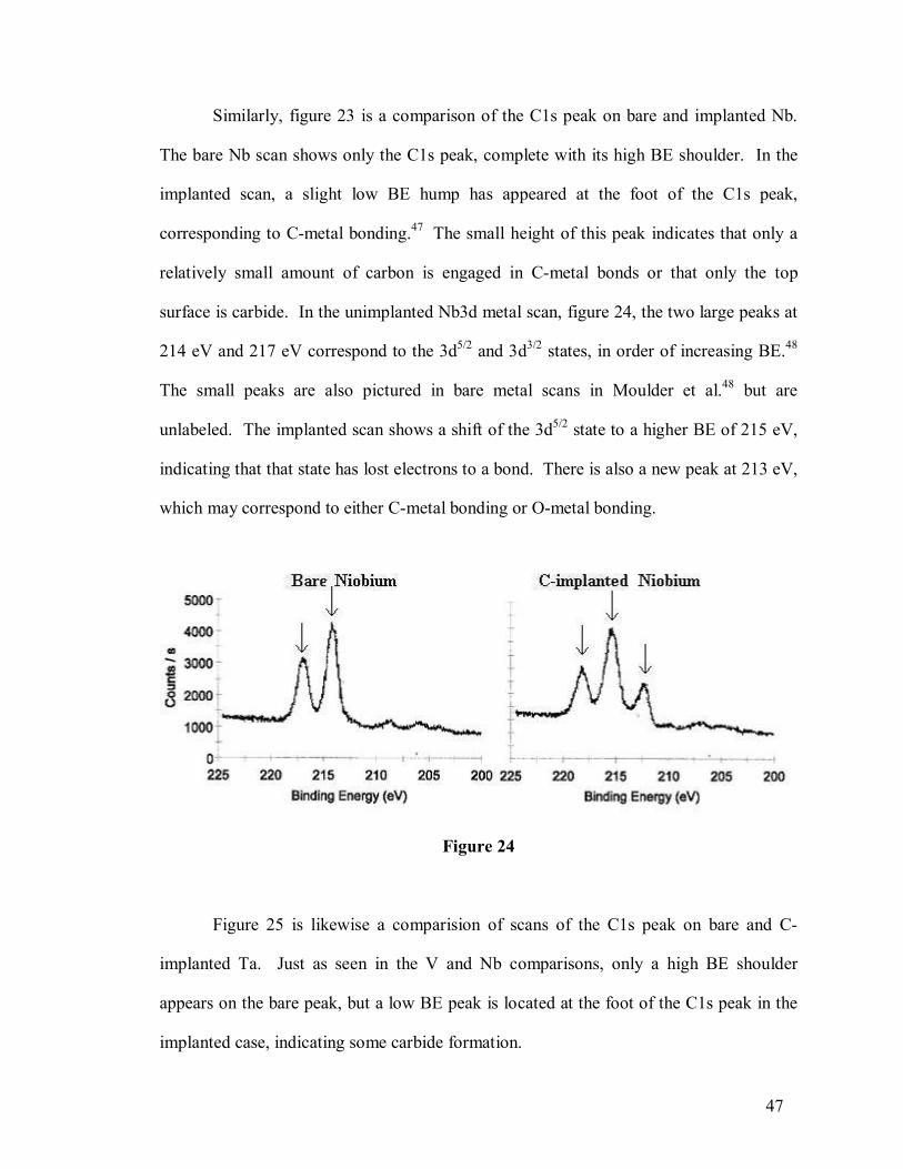
Similarly, figure 23 is a comparison of the C1s peak on bare and implanted Nb.
The bare Nb scan shows only the C1s peak, complete with its high BE shoulder. In the
implanted scan, a slight low BE hump has appeared at the foot of the C1s peak,
corresponding to C-metal bonding.47 The small height of this peak indicates that only a
relatively small amount of carbon is engaged in C-metal bonds or that only the top
surface is carbide. In the unimplanted Nb3d metal scan, figure 24, the two large peaks at
214 eV and 217 eV correspond to the 3d5/2 and 3d3/2 states, in order of increasing BE.48
The small peaks are also pictured in bare metal scans in Moulder et al.48 but are
unlabeled. The implanted scan shows a shift of the 3d5/2 state to a higher BE of 215 eV,
indicating that that state has lost electrons to a bond. There is also a new peak at 213 eV,
which may correspond to either C-metal bonding or O-metal bonding.
Figure 24
Figure 25 is likewise a comparision of scans of the C1s peak on bare and C-
implanted Ta. Just as seen in the V and Nb comparisons, only a high BE shoulder
appears on the bare peak, but a low BE peak is located at the foot of the C1s peak in the
implanted case, indicating some carbide formation.

48
Figure 25
Figure 26 is again a comparison of the metal Ta4f region for bare and implanted
samples. The bare sample shows four peaks, two of which are the 4f7/2 state at 35 eV and
the 4f5/2 state at 37 eV as identified by Moulder et al.48 The other two are identified by
Riggs and Parker31 as tantalum(V) oxide. In the implanted case, the Ta4f peaks shift up
to 37 eV and 39 eV, the tighter hold indicating a loss of electrons from that orbital, and a
third peak at 34 eV, likely a C-metal peak. The metal-oxide peaks have contracted,
perhaps due to displacement by carbon during implantation.
Figure 26

49
D. AFM Data
Material Ra Std Deviation Rq Std DeviationV Bare 12.2 nm 2.0 nm 16.0 nm 1.8 nmV C-implanted 24.1 nm 2.5 nm 29.8 nm 2.6 nmNb Bare 114.4 nm 26.6 nm 144.3 nm 25.3 nmNb C-implanted 100.9 nm 22.3 nm 125.6 nm 24.8 nmTa Bare 129.0 nm 53.8 nm 159.4 nm 68.8 nmTa C-implanted 117.06 nm 49.6 nm 145.13 nm 68.8 nm
Table 3
Table 3 is a table of average surface roughness measurements on bare and C-
implanted group 5B metals. Measurements were taken over five areas of 5 µm x 5 µm
for each sample and computed by arithmetic averaging for Ra and the root mean squared
method for Rq. According to these data, implantation approximately doubled the
roughness of the vanadium foil but had little effect on the rougher niobium and tantalum
foil. Perhaps the effect of carbon deposition onto rougher surfaces is a small factor when
compared with the surface features that existed before implantation. In these
measurements, the standard deviation values also provide an indirect measurement of
surface roughness. Naturally, a greater degree of variation is expected from surfaces with
more prominent features. Figures 26 through 28 are AFM images of surfaces of
vanadium, niobium, and tantalum, respectively.
It is difficult to directly relate these measurements of surface roughness to
effective work function calculations that appear in table 1. While virtually no
enhancement in work functions of vanadium and tantalum due to implantation was
calculated, the roughness of vanadium increased on the order of twofold. Moreover, even
though the work function of niobium was increased by ~ 0.5 eV, the roughness remained

50
constant within one standard deviation. Effective work functions for niobium, however
are ~ 0.9 eV higher than accepted values, which seems inconsistent with prominent
surface features on the sample, just as the ~ 0.2 eV difference of observed over accepted
work function values on bare Tantalum is not explainable by surface roughness.
Figure 27: Vanadium

51
Figure 28: Niobium
Figure 29: Tantalum
52
V. Conclusion
Because of current limits of the STM, all I-V curves produced within the
linearization region were not analyzable using the Fowler-Nordheim equation. At larger
tip-sample distances (greater than ~1.5 nm), more voltage may be applied before reaching
the current ceiling and traditional exponential behavior is observed. Below this range,
linearization can be traced by modeling data as the product of a voltage with an
exponential, and for tip-surface separations of less than ~0.7 nm the exponential
approaches unity. Based on linear approximation models of STM I-V curves at low
voltages, no significant work function enhancements were seen on C-implanted V and Ta
outside of the uncertainty in measurement. On niobium samples, a work function
enhancement of 0.51 ± 0.02 eV was observed after implantation. The discrepancy
between observed and accepted values of the work function of bare niobium may be
explained by the low reflectivity of the surface; STS requires a conductive and very
smooth surface for stable electron currents. Little information can be gleaned from

53
density of states measurements plotted as dVdI
VI 1−
against V, which are dominated by
noise due to integration over discontinuous current resolution at lower voltages. Kelvin
probe measurements taken on a the sample foils indicate similar field emission
enhancements for vanadium and niobium samples – a small enhancement of 0.04 eV for
vanadium and a significant decrease of 0.56 eV for niobium. KP measurements of the
tantalum foil, however, show a ∆CPD of 0.65 eV, even though STS measurements
showed no significant change. A possible explanation is that the relatively small amount
of data points below the STM current limit prevented an accurate calculation of the I-V
slope. XPS BE scans of the bare and implanted metals revealed a low energy shoulder or
subpeak 2 to 3 eV below the C1s peak in each of the implanted specimens, corresponding
to carbide formation, even if it is well below stoichiometric levels. Scans of the metal
peaks also exhibited signs that can be interpreted as carburization or oxidation. AFM
surface roughness measurements did not correlate well with work function
enhancements. Only V samples displayed substantial signs of increased roughness after
implantation, although the more irregular Ta and Nb foils may have experienced a similar
increase that was masked by their rougher initial surfaces. Further research with a more
powerful STM is necessary to accurately describe FN behavior of Group 5B in the 1 to 3
V region and thus calculate work function enhancement and particularly to view DOS
plots, which typically become interesting in the region of 1 to 4 V.
54
Appendix I: Tunneling Currents Measured with respect to Gap Distance
55

56

57
Appendix II: Tunneling Currents Measured with respect to Bias Voltage

58

59

60
VI. Acknowledgements
The author extends his sincere gratitude and admiration to Dr. Dennis Manos for
his extraordinary knowledge of surface physics and his role as editor, advisor, and
mentor. Nimel Theodore has earned great appreciation as a guide and an endless source
of experience and advice. The author further expresses his deep appreciation to Amy
Wilkerson for her expertise with all manner of experimental surface analysis and to
Christine Hopkins and Natalie Pearcy for their companionship and technical experience.
He would also like to express a debt of gratitude to Mingyao Zhu for the SEM images
and Michael Bagge-Hansen for the last-minute Kelvin probe data. Their contributions
have added a considerable depth to this work. Additional thanks go to Dr. Brian
Holloway and Dr. Henry Krakauer for their contributions and service on this examination
committee. Funding on this project was provided by the Governor's Commonwealth
Technology Research Fund (CTRF).

61
VII. References
1 W. Zhu, G.P. Kochanski, S. Jin, L. Seibles, D.C. Jacobson, M. McCormack, A.E. White, Appl. Phys. Lett. 67, 1157 (1995). 2 N.A. Fox, W.N. Wang, T.J. Davis, J.W. Steeds. P.W. May, Appl. Phys. Lett. 71, 2337 (1997). 3 T. Ito, M. Nishimura, A. Hatta, Appl. Phys. Lett. 73, 3739 (1998). 4 Y.T. Jang, C.H. Choi, B.K. Ju, J.H. Ahn, Y.H. Lee, Thin Solid Films 436, 298 (2003). 5 W.M. Tsang, S.P. Wong, J.K.N. Lindner, Appl. Phys. Lett. 81, 3942 (2002). 6 D. Chen, S.P. Wong, W.Y. Cheung, W. Wu, E.Z. Luo, J.B. Xu, I.H. Wilson, R.W.M. Kwok, Appl. Phys. Lett. 72, 1926 (1998). 7 R. Gomer, Field Emission and Field Ionization (AIP, New York, 1993). 8 W.A. Mackie, J.L. Morrissey, C.H. Hinrichs, and P.R. Davis, J. Vac. Sci. Tech. A 10, 2852 (1992). 9 W.A. Mackie, J.L. Morrissey, C.H. Hinrichs, R.L. Hartman, and P.R. Davis in Tri-Service/NASA Cathode Workshop, 1992 Proceedings, edited by J.W. Gibson (Palisades Institute for Research Services, Washington D.C., 1992).

62
10 W.A. Mackie, R.L. Hartman, and P.R. Davis, Appl. Surf. Sci. 67, 29 (1993). 11W.A. Mackie, T. Xie, and P.R. Davis, J. Vac. Sci. Tech. B 13, 2459 (1995). 12W.A. Mackie, R.L. Hartman, M.A. Anderson, and P.R. Davis, J. Vac. Sci. Tech. B 12, 722 (1994). 13W. A. Mackie, T Xie, J.E. Blackwood, S.C. Williams, and P.R. Davis, J. Vac. Sci. Tech. B 16, 1215 (1998). 14 T. Xie, W.A. Mackie, and P.R. Davis, J. Vac. Sci. Tech. B 14, 2090 (1996). 15 W. A. Mackie, J.L. Morissey, C.H. Hinrichs, and P.R. Davis, J. Vac. Sci. Tech. A 10, 2852 (1992). 16W. A. Mackie, T. Xie, M.R. Matthews, B.P. Routh, and P.R. Davis, J. Vac. Sci. Tech. B 16, 2057 (1998). 17D. Chen, S.P. Wong, W.Y. Cheung, W. Wu, E.Z. Luo, J.B. Xu, I.H. Wilson, and R.W.M. Kwok, App. Phys. Lett. 72, 1926 (1998). 18 W.M. Tsang, S.P. Wong, and J.K.N. Lindner, App. Phys. Lett. 81, 3942 (2002). 19 W.A. Mackie, P.R. Davis, Proc. 6th International Vacuum Microelectronics Conf, 34 (12-15 July, 1993). 20 A.P. Burden, International Material Reviews, 46, 213 (2001). 21 R.J. Hamers and D.F. Padowitz, “Methods of Tunneling Spectroscopy with the STM,” in Scanning Probe Microscopy and Spectroscopy: Theory, Techniques, and Applications, 2nd ed, D. Bonnell, (ed.) (Wiley-VCH, New York, 2001). 22 R.H. Fowler and L. Nordheim, Proc. Roy. Soc. London, A 119, 173 (1928). 23 S. M. Sze, Physics of Semiconductor Devices (Wiley, New York, 1981). 24 J.C. Miller, “The Role of Adsorbates on Field Emission” (Physics B.S. Thesis, College of William and Mary, Virginia, 2002). 25 R. Smoluchowski, Phys. Rev. 60, 661 (1941). 26 Y. Hasegawa, J.F. Jia, T. Sakurai, Z.Q. Li, K. Ohno, and Y. Kawazoe, “Mesoscopic Work Function Measurement by Scanning Tunneling Microscopy,” in Advances in Scanning Probe Microscopy, T. Sakurai and Y. Watanabe (eds.) (Springer, Berlin, 2000). 27 A. Anders, Handbook of Plasma Immersion Ion Implantation and Deposition (Wiley, New York, 2000).
63
28 J.T. Scheuer, M. Shamim, J.R. Conrad, J. Appl. Phys. 67, 1241 (1990). 29 L. Wu, “Surface Processing by RFI PECVD and RFI PSII” (Ph.D. diss., College of William and Mary, Virginia, 2000). 30 T. Ohno, “The Theoretical Basis of Scanning Tunneling Microscopy for Semiconductors – First-Principles Electronic Structure Theory for Semiconductor Surfaces”, in Advances in Scanning Probe Microscopy, T. Sakurai and Y. Watanabe (eds.) (Springer, Berlin, 2000). 31 K. Siegbahn, C. Nordling, G. Johansson, J. Hedman, P.F. Hedén, K. Hamrin, U. Gelius, T. Bergmark, L.O. Werme, R. Manne, and Y. Baer, ESCA Applied to Free Molecules (North-Holland, Amsterdam, 1969). 32 W.M. Riggs and M.J. Parker, “Surface Analysis by X-ray Photoelectron Spectroscopy,” in Methods of Surface Analysis, A.W. Czanderna (ed.) (Elsevier, Amsterdam, 1975). 33 W.S. Vogan, “The Effect of an Adsorbate upon Secondary Emission Properties of Low-Energy Ion Bombarded Metallic and Semiconductor Substrates” (Ph.D. diss., College of William and Mary, Virginia, 2003). 34 J. Bardeen, Phys. Rev. Lett. 15, 57 (1961). 35 J.A. Stroscio and R.M. Feenstra, “Methods of Tunneling Spectroscopy,” in Scanning Tunneling Microscopy, J.A. Stroscio and W.J. Kaiser (eds.) (Academic Press, Boston, 1993). 36 N. Sasaki and M. Tsukada, “Theory of Scanning Probe Microscopy,” in Advances in Scanning Probe Microscopy, T. Sakurai and Y. Watanabe (eds.) (Springer, Berlin, 2000). 37 J. Tersoff, “Theory of Scanning Tunneling Microscopy,” in Scanning Probe Microscopy and Spectroscopy: Theory, Techniques, and Applications, 2nd ed, D. Bonnell, (ed.) (Wiley-VCH, New York, 2001). 38 E.J. van Loenen, J.E. Demuth, R.M. Tromp, and R.J. Hamers, Phys. Rev. Lett. 58, 373 (1987). 39 J.A. Stroscio, R.M. Feenstra, and A.P. Fein, Phys. Rev. Lett. 57, 2579 (1986). 40 M.L. Yu, B.W. Hussey, E. Kratschmer, T.H. Philip Chang, and W.A. Mackie, J Vac. Sci Tech B. 14, 3797 (1996). 41 Y. Kuk, “Metal Surfaces,” in Scanning Tunneling Microscopy, J.A. Stroscio and W.J. Kaiser (eds.) (Academic Press, Boston, 1993).

64
42 N.D. Theodore, D.M. Manos. HBES Review. 20 January 2003. 43 L.A. DeJong, “Plasma Source Ion Implantation for Improved Surface Hardness of Stainless Steel” (Physics B.S. Thesis, College of William and Mary, Virginia, 1997). 44 M.J. Eccles, M.E. Sim, K.P. Tritton, Low Light Level Detectors in Astronomy (Cambridge University Press, 1983). 45 R.A. Outlaw, “Transition Metal Carbides (TMC): Single Tips to Thin Films, Mackie et al.” HBES Project, (College of William Mary, Virginia, September 17, 2003). 46 K.L. Barbalace, “Periodic Table of Elements.” Internet online. http://www.environmentalchemistry.com/yogi/periodic/#periodic%20table%20of%20elements, [15 April 2004]. 47 T. Fujihana, Y. Okabe, M. Iwaki, Surface and Coatings Tech. 66, 419 (1994). 48 J.F. Moulder, W.F. Stickle, P.E. Sobol, K.D. Bomben, Handbook of X-ray Photoelectron Spectroscopy: a Reference Book of Standard Spectra for Identification and Interpretation of XPS Data (Physical Electronics, Eden Prairie, 1995). 49 J.E. Castle, Surf. Interface Anal. 33, 196 (2002).