
FIBER OPTIC ROTATION SENSOR - Dr. Edward … Phaaa Modulation with resonant £requency o£ piezo C...
49
FIBER OPTIC ROTATION SENSOR A MaJor Qualifying ProJect subaitted to the faculty of WORCESTER POLYTECHNIC INSTITUTE In partial fulfillaent of the raquireaant for the Degree of Bachelor of Science by May 3 1985 approved: _____________ _ Den H. Wolaver
-
Upload
nguyendiep -
Category
Documents
-
view
217 -
download
0
Transcript of FIBER OPTIC ROTATION SENSOR - Dr. Edward … Phaaa Modulation with resonant £requency o£ piezo C...

FIBER OPTIC ROTATION SENSOR
A MaJor Qualifying ProJect subaitted to the faculty of
WORCESTER POLYTECHNIC INSTITUTE
In partial fulfillaent of the raquireaant for the Degree of Bachelor of Science
by
May 3 1985
approved: _____________ _
Den H. Wolaver

":::.:-: ... ~ · . . :··-' : -~~-
;.-.~ .. .'•':." .
• • 1 .... .
. _·;·::. ... . ''1'':_;.:,
-·-·------
. -~. : ~:!
.····:':
... _;_,_ ..
... ___________ _ ___ ..,.._
··--~.,=-~-- .. ~.
-·-
•ca··· La
.,.;. - ~·
.. ·::,·-... ·
. . ·::·_::. .. :-·- ~:. . . ·~ : .

TABLE OF CONTENTS
I Introduction A Overview B Fiber Optics Hiatory C Ita rola with rotation aenaora D Accoapliahaenta aade in £iber optic rotation sensing E Future application• £or FORS
II Background - Fundaaentala A Sagnac Theory B Reciprocity c Phase Modulation
III Optical Design A Syatea Layout B Phaaa Modulation with resonant £requency o£ piezo C Sensitivity
IV Electronic Design A Optical :Source B LED Driver c Cooler D Photodetector and Aapli£ier E Linear Multiplier F Integrator G Vi rtual Ground H Tiaera I Crystal Oscillator
V Suaaary o£ Space Ready Syatea A Weight B EDAS interface C Physical Mounting D Power Conauapt.ion
VI Appendices A Fiber splicing B Circuit Diagram C Piezo Calculations D Testing E Phaae Modulated Output va. Rotation F SNR Calculations £or the Integrator G Cooler Design H Piezo Oscillator I Acknowledgeaenta J What ia Le£t to be Done
VII Endnotes
- 1 -

CHAPTER ONE
I A Overview
Our proJect ia the design and construction o£ a fiber
optic rotation aensor. It is part o£ the MITREIWPI Space Shuttle
prograa. It ia to be launched aboard a 1986 Space Shuttle
flight. and would aeaaure the rotation o£ the apace shuttle about
ita roll axis. The data ia atored on aagnatic tape by another
proJect. the Enviroaental Data Acquisition Tea~. and returned to
earth. where another proJect teaa would coapare thea against
rotation inforaation that we hope to receive froa Naaa.
A beam o£ light ia split by a fiber optic coupler, and
the resulting beaaa are £ad into the opposite ends of lka of
fiber wrapped around a loop. When the counterpropagating beaaa
exit the opposite ends of the fiber, they are recoabined. I£ the
loop waa rotating when the beaas were traveling in it, one beaa
would travel a longer distance than the other, and thereby
acquiring a phase shift relative to the other. When the two
beaas are recoabined, the intenaity of the resulting light wave
would depend on the phaae shift between thea. By detecting the
resulting intensity, the phase shift, and therefore the rotation
rata ia deterained.
- 2 -

I B Fiber Optics History
The incentive £or £ibar optics technology occurred in
1966. when the use o£ glaaa fibers waa £irat auggeated. Since
then, the largeat activities were in reducing the fiber
attenuation £roa aaveral hundred of dB/Km to an incredible 0.2
dB/Ka. In parallel to thia, aany other coa ponents £or optical
linka ware developed, the a oa t d i f ficult o£ which was a reliable
aolid sta te l aaer.
I C Ite Role Wit h Rotation Senaors
The use o£ count er propagati ng light baaaa in rotation
sensi ng was first deaonatr ated by G. Sagna c i n 1913 (1-1>. He
showed t hat count e r popagating l i ghts travelling in a loop
inter£eroaeter a c quired a phase difference if t he light path waa
rotating about i ta axia . Howe ver, becaus e of the large light
patha required, ita aensitivity was axtreaely liaitad.
A aaJor iaprova aant in the aenaitivity of rotation
sensors waa aade poaaible through the development o£ the laaer.
The ring laser g yroscope, £iret deaonatrated by Macek and Davia
in 1963 <1-2), enlarges the effective light path by recirculating
the beaa aany tiaaa in an active reaonant cavity. The ring laaer
gyroscopes are currently being uaed in Boeing 757 and 767
aircrafta <1-3>.
1976
The
by v. £irat
Vali
fiber optic rotation aenaor waa developed in
and R. W. Shorthill <1-4>. It ia a "paasive"
inter£eroaeter because in this caaa the light path ia a length of
- 3 -

fiber, aa opposed to the ring laaer gyro, whoa• light path ia
inside the active device, the laaer.
I D Accoapliahaente ~ade in fiber optic rotation aenaing
With the developaent o£ extreaely lowlosa optical fibara
(0.1 dB/Ka or leas>, increasingly longer length& of fiber can be
used in rotation aenaora, thereby increasing the sensitivity.
Alao, iaproved procedures in phase biasing and polarization
control, and aetupa guaranteeing reciprocity between the counter
propagating beaaa decrease the signal to noiae ratio, and thereby
iaprove sensitivity.
Ultiaate sensitivities of 1£-S deg/ hr have been
predicted, and currently, aenaitivitiee of 0.1 deg/ hr have bean
achaived <1-S>.
I E FUTURE APPLICATIONS FOR FORS
Fiber optic rotation aenaor
accelerating rapidly over the peat
were built for testing in 1983-84,
<FORS> reaearch haa bean
decade. Flying prototypaa
leading to their initial
production,
unit will
deg/hr.<1-6>
for operational uee, in 1984. The firet production
have aodeat perforaance, with drift on the order of 10
Over the next decade, fiber optic rotation aenaing
production will expand iapreaaively, and reach into •12s aillion
in 1994.(1-7> Thia will in turn raault in an all fiber optic
- 4 -

baaed guidance ayatea production including gyroacopee (3 rotation
aenaora £or the X-Y-Z direction>. acceleroaetera. electronic••
and packaging.
There have been maJor contributors in the area o£ FORS.
In 1984, KcDonnell-Dougl&a Astronautic• are nearest to production
o£ a rotation aenaor o£ better than 1 deg/hr. while Litton
Guidance and
aansor with
Nearly all
per£oraance
Controla have developed a laboratory baaed rotation
a navigation grade better than 0.01 deg/hr.<1-8)
o£ the growth over the next decade will be in lower
unita with a drift rate o£ 1 dag/hr. Many technical
probleaa, such as unbalancing teaperature change effecta and
light re£lectiona reaain to be aolved before the FORS can coapete
with the ring laaer gyro and the aass apinning gyro in the 0.01
deg/hr, and better, drift region.
- 5 -

CHAPTER TWO
II A Sagnec Theory
In diacuaaing the pheae relationahip between two
counter propagating lightwave• in a rotating optical fiber loop,
one •uat firet underatend the Sagnac effect. Aa reaeerched by
laat yeara FORS proJect team it waa determined that for a
stationary inter£ero•eter ahown in fig 2.1, that two lightwavea
launched into oppoaite enda of a fiber loop return back to either
and in phaae, after a propagation tiae T.
Where T = 2piR
c
so/5"0 "' ~- R or- ---
L_
·-
FlG-. 2. I
- 6 -

Siailarly, when the intar£eroaater ia rotating at a rata w aa
abown in fig <2.2> , and tba LED, photodatector and electronic&
are alao rotating in the inertial fraae, then a aeaauraaent o£
the rotation rata can be made when pt.P aovee through an angle wt
during propagation time t. Therefore the difference between
propagation timea :
2 dT = <2pi + wt>R - <2pi - wt>R • 4p1R w
c c
The phase shift bet ween the t wo lightwave&
2 d9 • Wdt • 4p1R W ~
2 c
2 c
The two phaee ahifts add contr uctively and deatructively, and we
aee t he final effect of t he t wo wavea being
2 9 • d9 • 8pi W N A
cy
It ia interesting to note that the Sagnac effect ia due to a
di££erence in propa gation time around a rotating loop,
independent o£ the velocity (c) o£ the phyaieal phenoaenon which
ie used. The wave f requency aervea aa a clock to measure thie
tiae differe nce: the higher the frequency, the larger the
reaultant phase difference <2-1) .
- 7 -

Comments on page 81
When the system is rotating at a rate w
Point Pi moves through angle wT during propagation time T
The difference between propagation times o£ counter propagating waves in the loop is
2 dT = C2pi ~ wdT>R - (2pi - wdT>R = 4pi R w
c c
dT - difference in propagation time R - radius of loop w - rotation rate c - speed of light
The phase shift between the lightwaves
2 d9 = WdT = 4pi R W w
2
W - phase stn.:ft. bet:.ween l1.gh~ ""aves
2B ~ d8 = Bpi R W w
- 8-
2 c

II 8 Reciprocity
The two light beaaa that are to be compared in phaae auat
have the exact aaae hiatory in order £or total cancellation to be
poaaible. However, i£ only one coupler is uaed aa in £ig. 2.3a,
the beaa propagating clockwiaa would undergo a reflection
<coupling) upon entering the loop , and another reflection when
going into the receiver. Meanwhile, the counterclockwise beaa
would undergo two tranaaiaaiona. Theae two light beaaa do not
have the same hiatory, and therefore, their coapariaon ia not a
valid one. However, i£ the two- coupler configuration of fig.
2.3b ia uaed, e a ch beaa, in going £roa the light aource to the
detector, gets tranaaitted
have the aaae
twice and reflected twice.
history, and therefore, light beaaa
coapared, resulting in a valid fringe pattern.
- 9 -
The two
can be

I f?
T
( (".)
t>{IU) <" u () ~
A. I~
ILF() I 11.
I J ->
. --~
T
~-")· z..1
-\¢-

II C Phaae Modulation
The light intenaity at the detector ia at ite aaxiaua
with no phase ahi£t between the counterpropagating baaaa~ and
deer••••• with increased phaae ahi£t (2-2>:
I<out> • I<max)/2 (1 + coa d9 >
Aa you can see fro• fig. 2.4a~ aaall pha .. ahifta which our
syat•• ia anticipating~ reault in •xtreaely ••all changea in
light intenaity becauae we are on th• aoat in .. naitive portion of
the curve. Alao~ positive and negative phaae ahifte o£ the ••••
aagnit.ude reault in identical ••dipa" in output intenaity~ and are
t.hua indiatinguiahable. Idoally~ we would like to apply a
nonreciprocal pha•• ahift of -90 degrees~ in addition to the dO
due t.o the Sagnec Effect:
I<out.> a I<aax>/2 [1 + coa< de - 90 >l • I<max)/2 <1 + ain d8 )
Thia would require extremely high-frequency puleing of the light.,
and extensive control and pulaing circuitry <2-3>. Another
aethod of achieving the aame phaae bias ia by applying a
ainuaoidal phaae aodulation. Aa ahown if fig. 2.4b, a ainuaiodal
phaae biaa of frequency F would reault in the output varying with
frequency 2F. I£. due to rotation, a conatant. phaae ahift. ia
- 11 -

added to the ainuaoidel biea <aee fig. 2.4c end d), the output
wevefora would have a coaponent varying at the fundeaental
aodulation frequency, F. It can be ehown (aee appendix E> that
the coaponent of the output aignal varying at the fundaaental
frequency hac t he fora:
I(fund>=I<max>/2 J,<2/0 ain wT/2 ) ein d8 sin wt
where
d9 = Amplituda of the induced phaae ahift between the two light•
w o Fundaaental frequency of aodulation in rad/aec
T = travel tiae of the light through the fiber
lt = the firat order Beaael function of the first kind.
To aaxiaize the eaplitude of the fundeaantal frequency
coaponent. which contain• the rotation inforaation, the value of
the arguaent of the Baaael function waa optiaized at 2~0ainwt/2 = 1.8 radians.
By aultiplying
the sinuaoid driving
fundamental coaponent
the aignal out of the light detector with
the phaae modulator. the apectrua of the
would be shifted to d.c <aea fig.
2.Se,b,c). It can than be retrieved aa a conatant voltage by
integrating the output of the multiplier. Thia would elao
ainiaize the effect of any drifta in the aodulation frequency.
Thia aethod ia explained in aore detail in aectiona III-B and
IV-I.
- 12 -

l'i .L
J
/_' -A v
(
• I
-" r __ if'J_-, --1
:.. r -rf.:\. -_v_ - -

F zr
( --_ l __ l _
F (h)
~--t_ f tF F F lf
- 1'1 -

CHAPTER THREE
III A> Syatea Layout
The ayatea diagraa o£ the £iber optic rotation aenaor ia
ahown in £ig. 3.1. A£ter receiving a atrobe pulae on the
••ready"" line froa the data acquiait.ion circuit. Cwhich retreivea
our data once every 10 aeconda and etorea it>, the ayatea
controller waita for approxiaately 9 aeconda and then pulaea the
light eaitting diode for a duration of SO ailiaeconda. The light
travels through the
loop. The counter
two couplera, the phaae aodulator, and the
propagating beaaa are recoabined when they
re-enter the aecond coupler. The reaulting wave travale back
through the £irat coupler, and into the detector, which convert•
light intenaity into current. The current is converted to a
voltage, and aaplified by the tranaiapedance aaplifier. The
resulting voltage ia £ed into the multiplier, which convert• the
£undaaantal frequency coaponent into a d.c. aignal by aultiplying
it with the aodulation ainewave. It is then averaged out by the
integrator and atored as a voltage on a capacitor for the EDA to
pick up.
The local detector aonitora the output light intenaity
through a feedback loop, to coapenaate for any drift in the LED
or driver circuitry characteriatica. It ia eaaential that the
light intenaity reaain conatant becauae the output aignal ia
directly proportional to it.
- 15 -

$_. - ~, .. '
~
'
I I
l l
1300 nm
I., ED ! -..
SYSTEM TIMING
j
"READY" LINE
0
WPI/Mitre Rotation Sensor
3 dB COUPLERS
(f 3 DEAD END
(C 1
PIN DET
PREAMP
• LOCAL
DET
•7 0.4m 1 km
DIAMETER FIBER
P LOOP
ZT
110kHz OSCILLATOR
MULTIPLIER I• . I
I .. I INTEGRATOR 14 I
TO STORA~E ON MAGNETIC TAPE
~\'j ..
. ,.
~ . '

III B Pheae aodulation with piezo
Phaae aodulation o£ the light in the fiber loop occura
with the help of a pie2o electric cylinder. Piezo electric
cryatala can convert action into an electric voltage, and vice
we apply an electric field onto a
it will expand in the direction
of the electrode. Our cylinder haa
In other warda, if
piezo electric crystal,
alectrodea on ita outaide and inaide, and will therefore expand
radially.
We uae our piezo by winding aeveral turna o£ fiber around
the cylinder, and applying a ainuaoidel voltage on ita
alectrodea. The resultant expanaion of the cryatal cauaea the
light path length to change ainuaoidally. Thia continual change
in path length cauaaa a near ainuaoidal change at twice the
frequency in the light laval that the detector ••••· Pleaaa
refer to Fig. 2.4b.
Both the aaplitude and the frequency of the voltage
applied to the piazo can be optimized to beat suit our naada. We
know £roa peat calculations that the aaplitude of the fundaaental
will change aoat groetly with the aema rotation if we aoduleta
the piezo ao the minimum light level at the detector ia 38.6X of
the peak light level, aa ia derived in Appendix E. To optiaize
the voltage on the piazo, we conaidar that the aultiplier waa
designed to accept e 2 Vp-p aignal aa input fro• the piezo.
- 17 -

Theae two criteria eatabliahea a unique aaount o£ turna around
the piezo. Froa experiaentation and calculation• we deterained
that the aaount of turna around the piezo should be about 20.
Pleaee aee Appendix c. Previoua calculations using conatanta
aupplied be the piezo aanu£acturer, Vernitron, indicated that we
ahould drive the piezo at 3 Vp-p and at 60 turns to achieve
roughly the •••• reault. Tbia reaarkable increaae in a££iciency
can be attributed to ua operating the piezo at ita reaonant
frequency.
The beat frequency at which to drive the piazo can be
found by looking at the aiaple illuatrationa below.
Fig.3.2a Fig.3.2b
Here we aee two grapha that &how light path length va. tiae. The
packeta o£ light bit the piezo about S aicroaeconda apart. The
firat hit occur• when one light wave leavea the coupler and
alaoat iaaediately enters the piezo. The aecond hit occura when
the light wave that went the other direction baa gone through the
loop and goea through the piezo. Aa we can ... , the light
packeta in Fig.3.2a experience a aaaller relative ahift than in
Fig. 3.2b. The beat ahi£t occura when the light packet• hit the
piezo 180 degr••• out o£ phaae. Thia fixes the beat frequency
to be
- 18 -

4 ''D . ,, omm nv~
''G-rooVId .,
\'3

1 L
£ = ---------------------------- J T • -------2
Jf
where:
c T
£ - optiaua frequency T - tiae it takea light to go through loop M - 1~3~~~7~9~··•······ L - Len.th of loop ~ 978 aetera c - Speed of light in loop = 2 E 8 a/a
In our caae. K•1~ T•4.89 aicroaecond•~ and £~ 102.250 kHz.
Aa waa aentioned earlier. a piezo converta electric
energy into aechanical energy~ and vice versa. To fully
underatand the piezo we iaolated a piece o£ the electrode by
cutting into the outer ailver foil . Pleaae aee Fig. 3.3 This
"'feedback a trip" ia 4aa wide~ in contraat to the total
circumference o£ the piezo which ia 40aa. This strip becaae an
output~ with the reat of the outaide aa input, and the inside the
coaaon. To inveatigate the properties of the piezo we did a
apectral plot of ita output. sweeping the input frequency from DC
to 180 kHz. The piezo ahowa aeveral peeka in ita reaponae~ with
a aaxiaua at 108 kHz. please aea Fig. 3.4. Our initial plan was
to uae a cryatal oacillat.or to keep the frequency at about 40 kHz
becauae the frequency plot ehowad a very flat curve at. that
point. Thia would ainiaize any effects of teaperatura. This
echeae waa very inefficient becauae we now had two crystals do
deal with~ each aubJect to drift due to t.eaperat.ure. A better
aethod would be to uae the piezo itael£ aa the oscillating
cryatel.
To explore thia poaaibility we probed further into the
cryatal#a properties. Uaing the LiaaaJoua pattern aethod we could
- 20 -

aeaaure the phaae ahi£t at varioua frequencies to see i£ there
waa anything intereating that we could uae. pleeaa see Fig 3.5.
The unique phaae ahi£t at 108 kHz enabled us to build an
oscillator that would reaain locked at the reaonance o£ the piezo
<maximum excuraion o£ the piezo>. and that oscillated near to the
optimum (mexiaua ahi£t with excuraion> frequency of the loop.
r\~) ttf + 35 liA R-rrV"ltA.ix
III C Senaitivity
Thia aection will diacuss the maxiaua poaaible
rotation rate that our ayatea can aeaaure with ainiaal rotation
rate error. With the uae o£ proper phaae biaaing, we can aake the
output intenaity vary •• the sine of the Sagnac phase shift.
Since we need a one to one correapondence between phaae ahi£t and
light output we can only aeaaure rotation rates resulting in a
phaae shift o£ up to 90 degreea aa shown in figure 3.6.
~0\1- -
Q
zsv ___ _;"3:o;·-=-" -1-.1......,:---4 --::-;-;.------i-.---........,.--;,.. :u: w~~..tt• W < o~::~/s£C)
OV-
__/ SL.OPI£: cos IS"" = . rjf,. CO.) o" I. oO
Fttc3.6
- 21 -

Using the Sagnac £oraula : 8pi W N A dB • ---------
cy
we deterained th• •axiaua rotation rate of our ayatea where
W : Rotation rate
N : • o£ turn• = 1122 2
A Area of the loop • .OS9 M
c : Speed of light <in vacuua> = 3E-8 N
y : Wavelength of LED • 1.3£- 6 N
With a aaximua poaaible phaae ahift <d9> of 90 degrees~ the aaxiaua rotation f o r our ayatea is W<max> ¥ 21 deg/aec. However~ ve are only expecting rotation ratea o£ -3.6 to +3.6 deg/aec. The EDA teaa axpecta an output voltage o£ OV to 5V. To aake uae o£ our entire alloted output rang•~ we are going to adJuat the gain• o£ the different atagea~ and eapecially the dif£erential aaplifier at the output of the aultiplier~ to have our output liaita correapond to -3.6 to +3.6 deg/aec. Thie would give ua a aenaitivity o£:
7.2 deg/ aec deg/aec ------------------- s 1.44 ----------
5 volts volt
- 22 -

CHAPTER FOUR
IV A Optical source
Our optical aource waa donated by Laser Diode Laba and
consists of four coaponenta in one aaall package : a cooler, a
theraiator, a detQctor, and an L.E.D. All the support circuitry
had to be deaigned for theae coaponenta, but wa unfortunately
received very little data on thea. This forced ua to perfora
teats on the device t o find out ita characteriati cs.
The theraiator is connected between pina 10 and 11 and
indicate• the teaperature inoide. We found that the resistance
decreaaed with increaaing teaperature. According to :
R • 33.3 - 0.3 F
where: F - Taaperature in Fahrenheit R - Thermistor resistance in kohm
The thermoelectric cooler ia siaply a theraocoupler
operated in revaree. In this mode a current cauaea a teaperature
difference between the outside o£ the package and the aubatrate
on which the LED ia aituatad. All we knew about thia cooler waa
that the aaxiaum allowable current wae 700 aA. Staying safely
away from thia value, we found the correspondence between the
- 23 -

current through the cooler and the taaperature drop inside.
CBecauee the cooler ia a thermocouple, we auapect that it will
alao heat tha laaer up i£ we reversed the current through it.
There is no need for ua to do ao in our application however,
because the temperature ahould not drop significantly below 0
degree• Centigrade.)
The LED ia the aoat critical o£ all coaponenta, and we
knew only that it had been puls0d to 400aA. We aet up a circuit
that pulaed it on at 200 aA £or 1aaec and turned it of£ for
100aaoc. The livht output waa aeaaured uaing tha detector we
already poaaeaed. Thia expariaent not only confiraed our belie£
that the LED waa eaitting light, but alao indicated to us how
much light waa bing eaitted (Fig. 4.1)o
Laatly, we attaapted to teat the detectora Unfortunately
I did not aucceed in getting any reaponae out of it. A V-I curve
trace ahowed an open circuit between pina 7 and 8, tha advertised
location o£ the local detector.
- 24 -

\ S""
\0
I I I 16 ~A
(ooler Cvrrek t
A"'bu.~v.t T~n.-.,.,~v-~tuvc : t9l df
LED off
~a HePtt Si :fl ~

~
-~"-~w ..... " ... .. 4
TTED I oUrwr
_1_ _
10
5
\oak
06T€(,T0{2 ~
o.7s ryw
Fig 4.1
cJoses+ ~ower c.orve f;t; 2.30~
..o 6 -s I :t'0 ;. u . 1·10 · L
JD i~ _/'A A
Tt c.,., n., A

IV B> LED Driver
Having a constant light in~enaity out of the super
luminescent diode i a essential in our proJect because the output
voltage i a directly proportional to the aaxiaua light intensity.
A eyatea diagraa o£ the regulated driver ie ahown in fig. 4.2.a~
and the circuitry accoapliahing this ia ahown in fig. 4.2.b. Any
drift in the characteristics of the LED or the driver circuitry~
cauaing a change in the light intensity. would ba reflected aa a
voltage drop acroaa the input terainala of the opaap, which would
in turn cau.. ita output to drift in the opposite direction~
thereby coapenaating for the drift.
At low frequenciea, the loop gain of the ayatea ia:
G<a>H<s>= <316K> [1/(lK-oha>l <40) (30 uWIA> (1/2) <.65 AIW> Rd
a 0.12 Rd
Since the value of Rd is approxiaately 500 K-ohaa, we have a very
large loop gain, and any aaall drift in the characteristics of
any of the coaponents would be coapenaated for very eaaily ~
The feedback loop haa an extremely £aat response, liaited
only by the alew rate o£ the op-amp. A circuit aiailar to the
LED driver waa tested £or response to pulsing <aee fig 4.3.a>.
The reference voltage was pulsed to a ""high"" of 2V, and the
voltage acroaa the 10-0ha resistor waa viewed on the acope. It
is reproduced in fig. 4.3.b & c. Aa you can aee, the emitter
- 26 -

voltage~ which datarainaa the driving currant atebilizea in about
30 uaec which ia negligible coapared to the ~0 asac pulaa.
When the actual circuit waa built~ it waa oacillating at
a frequency of 28.5 KHz. A ••zero•• was introduced in the ayatea
by placing a 43 uF capacitor in parallel with the 1 K-oha
resistor on the baae. The only aetback to this configuration is
a 1 msec delay in the reaponae o£ the ayat••~ which ia the tiae
required to charge up the capaitor~ before the baaa actually
riaaa.
We are planning to investigate the poaaibility of aoving
the base reaiator to the eaitter branch~ thua eliminating hfe
froa the loop gain. Thia would probably eliminate one of the
pole• in tha syat••~ atabilizing it with no need for the large
capacitor .
- 27 -

( (">)
_,_, -"i

+f
( o-)
IQ)
\ J
( o) ( (. )
\hr \~ < .. \ Scc..\t.: \ v I J: v \1 tf \;co.\ Su.\c. ~ ' -J I a.;~ "ur; l.~,.. \ o.\ ~ c:c;..\• ~ ;z.o,...~, / d,, v \\a.r: 1. .. "\r..\ Sco.\e l ~It, /J;v
- "t..'

IV C The Cooler
The
the LED baa
200 mA and
reaiator in
reaiatance o£ the cooler when the temperature inside
atabilized is 2 obaa. Aaauaing a cooler currant o£
a power aupply o£ 8 Volta, we would need a 38 oba
aeriea with the cooler to be able to hook it up to
the
the
power supply.
reaiator will
I£ we analyze thia aethod we will realize that
abaorb 9~~ of tho power o£ the two components
to raiae the ef£1c1ency o£ thia ayatea we coabinedt In order
auat reduce the voltage on the cooler not by dropping the voltage
acroaa a reaiator, but by pulaing the current through the cooler.
In e££ect we have a DC-DC converter that provides power on a
reduced voltage, but increaaed current l evel CFig 4.4>.
Although thia
e££1c1ency, it
aystea haa bought ua
ia not free o£ drawbacka.
- 30 -
a large increaae in
The pulsing puta a 60

aVolt ripple on the power aupply that can be filtered out
partially by a large capacitor.
The pulaer can be controlled by pin 4 on the tiaer, which
ia the reaet input. This line is controlled by a aiaple
coaparator, and when brought high will enable the cooler.
+d
The variable resiatance Rx aeta the teaperaturs at which the
cooler will awitch ON. In other warda, i£ the cooler ia set at 65
degreea and the aabient teaperature is 4~, the above circuitry
<Fig 4.~> will be OFF. I£, on the other hand, the teaperature
riaea above 6~. the cooler will turn on, cycling on and o££ to
aaintain the aaxiaua teaperature. This maximua teaperature ia :
F • 111 - 3.33333 Rx
- 31 -

..
IV D
A ailicon pn JUnction operating in aeriea with a back
biaaing voltage aupply and a reaistor, ia considered to be
operating in a photoconductive mode. Tbia mode o££era good
light-current linearity up to laW o£ optical power for a typical
lam diaaeter silicon diode.(f-1)
J I I -,ll
+v ==- I ! _) ~ \ I
For a photon to be aenaed, the aeaiconductor aaterial
auat elevate an electron ~roa the valence band to the conduction
band. Tbia createa an electron-hole pair, each o£ which
contribute• to the conductivity of the aaterial.
The expected range for signal current o£ our ayatea liea
between S and 10 aicroampa. Thia ia a reault o£ an LED output
power £roa the pigtail of SO microwatts, with splicing and fiber
loaaea aaaounting to 12dB (8?% loa• of the original power>,and a
reaponeivity of 0.8 A/W £or the detector. The operation o£ the
photodiode is dependent upon wavelength and detector aaterial,
being slightly teaperature dependent.
The signal current range has been eatabliahed, auat be
aaplified £rom microaapa to about 1 V peak-to-peak over the
aignal current frequency ranga o£ 220KHz. Thia requirea a
tranaiapedance o£ approxiaately 1 M-ohaa. We choae an aapli£ier
- 32 -

baaed on low supply voltage, wide band reaponae, high alew rate.
and low noiae. The frontend <preaaplifier and aapl1fier> uaed in
our prOJect ia ahown in figure 4.6.
C> -1V
-
A two-atage aapli~ication proceaa ia needed to provide the needed
tranaiapedance with a bandwidth o£ 220KHz. Due to nonlinearitiea
in the aapli£1er cauaed by the below apeci£ication voltage
auppliea of •-•v, the open loop gain A dacreaaed to 4~dB.
Paraaitic and internal capacitances a££ect the bandwidth
and £1atneaa oE reapon .. o£ the £rontend. An equivalent circuit
o£ t he preaap with internal capacitance o£ the op aap ia ahown
below. The signal bandwidth <B> o£ the tranaiapedance aapli£ier
is determined by the capacitor <C.> and the feedback reaiator <R>
divided by the aapli£ier1 e open loop gain <A> .
,!): :lOOK
A B • -------------- • 2~ MHz
- 33 -

C increaaea the pbaee ehift of the feedback loop thua cauaing
peaking.To offaet thia effect a feedback capacitor waa placed in
parallel with the E .. dbeck loop in order to flatten the reaponJ••
Figure <4.7> ahowa r eepon .. a for verioua C'a.
- 34 -

,
en I~
~ u 2 0 (:l.. 1/l lu
u
4
3
2
_.fiGr. 4 . '1
q ...
~---
·~
1
.... t
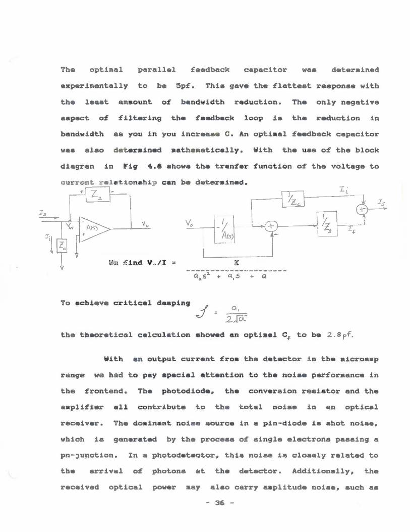
The optiaal parallel feedback capacitor waa deterained
experimentally to be Sp£. Thia gave the £latteet reaponee with
the leaat aaaount o£ bandwidth reduction. The only negative
aapect o£ filtering the feedback loop is the reduction in
bandwidth aa you in you increase C. An optiaal £eedback capacitor
waa alao deterained aatbeaatically. With the uae o£ the block
diagram in Fig 4.8 ahowa the tran£er £unction o£ the voltage to
current relationahip can be det.erained.
~-[g=--.
~-I L A(s)
I
\ [YzJ
J ~s :i?ind V .. /I = fi(
--Q~~2-:--~s--:--Q~---
To achieve critical deaping
the theoretical calculation ahowed an optiaal C~ to be 2.8pf.
With an output current £roa the detector in the aicroaap
range we had to pay apecial attention to the noiae per£oraance in
the £rontend. The photodiode~ the conversion reaiator and the
aapli£ier all contribute to the total noiae in an optical
receiver. The doainant noiae source in a pin-diode ia abot noiae,
which ia generated by the proceaa o£ aingla electrons paaaing a
pn-Junction. In a photodetector, thia noise is closely related to
the arrival o£ photone at the detector. Additionally, the
received optical power aay alao carry eaplitude noise, auch aa
- 36 -

LED noiae. A aodel for the noiae in a PIN diode can be
eatabliahed in fig <4.9).
------,-----------------~
1" 1o'!n. __J__ I p.r
-'-------...L....------- ·--o
Where the signal current.: i· s. RP
noiae . TIE 2eB<RP+l ) • .....
R . Reaponaivit.y of the Photodetector • 0.8 A/W •
p • Optical Power IE 7£-6 w •
e . Electron Charge = 1.6E-19 coul • . B : Moiae Equivalent Bandwidth = <220KHZ)pi/2
I : Dark Current • SE-9 A
aignal : I 5 • SE-6 a
noiae : ~ • 7.92E-20 A
The SM~ £or the dete ctor is 10 log ~ I ~· 130dB
f'l(.f 4.'t
The noiae contri buted by the aaplifier can be ahown in fig(4.10).
I 4kT~j);{ ·--[jfJ-
The no1•~ aourcea o£ the tranaiapedance a~plifier can be alaoat.
- 37 -

coapletely attributed to the input ataga in the preaap.
The average output noise: '( • R B<2eRf P + 2eit> + 4KT/R-r >
Where Rf: Feedback reaiator = 1.0E5 Ohaa
8 : Moia e equivalent bandwi dth • <220KHz>pi/2
e : Electron charge • 1.6E- 19 coul.
R : Reaponaivity o£ the det ector a 0.8 A/W
P : Average opti cal power • 5E-6 W
I~ : Dark currant = ~E-9 A
T : Degree• kelvin = 300 Deg . <Kelvin)
X : Bol tzaan'a c onatant = 8.62E- 5 eV/T
Sol ving t he a ve r age output noiae: V1 = 0.12 <uV>2 """
The detector output level : V = -R i • -0.8 V
The SKR a t t he output. of the preaap atage ia: V: I ~· 67d8.
Since we do not know the noiae level froa tho optica l ayatea. we
cannot. calculate t he SKR of the optica. Froa obaarvationa i n t.he
l a b. we aee a large aaount o£ noiae preaent on t he l ight. hitting
the final detector, and thia opti cal noiae i a higher than the
noise contributed by the electronic syatea.
IV E Multiplier
The aultipliar we uaad ia a 1595 made by Motorola. It ia
a chip that baa no direct connect.iona t.o the power aupply and
therefore required ua t.o aet up all biaa current• and internal
- 38 -

voltage• ouraelvea. Thia device aultipliea the aignala froa the
tranaconductance aaplifier and the piezo. Thia auliplication in
the time doaain reaulta in a convolution in the frequency doaain~
and the resul t i a tha t t he 105 kHz coa ponent froa the aaplifier
will ba a de signal at the output of t he aultiplier. We will
thua have a voltage proportione l to the rotation rate. This
signal i s t hen c oupled into t he i ntegrator t o filter out other
frequency coaponenta and noiae.
The output of t he aul t i pli e r ie :
And K =
V1 - front and input V2 - oscillator i nput
2 • 2000
X = ------------- = ----------~-------- • Oa24 3000· 3000• 0.0019
Ple••• ee e Fig. 4.12
- 39 -

·• .... . --..... ~~?~ ... ... h -·-~~~ I~
'""" -·· .... ~ · ~:;:~
MC 1595 +
+
'4 \j
L------+ 3 \1.
~ u---------f 4 l\
~s }0
'"---......;..._--+ b 1 .----1 7 a
\ '< \OfVT SuPf"L~ VOLT Q. Outtpvt 3 "! l n PVT S of PL 'I VOLT 4 Y lnPvr t+) ~ S Cftlll? Cr '( 6 ~ (. ~ u YJlf- ' '7 v-
mvl{, pll~r
+ +
J<,:;
v'l.
a '{ \n(UI (-) 9 X \nPVT C +) IO ->CRLlt1()- X. II ~<.ALih6- )( 11 X H\ 'f UT (-) ~~ X 'nr!'vr c;vpfl." VfA.I IY Ootrvt
. P.J Cf f)

IV F Integrator
The DC coaponent £roa the multiplier is proportional to
tbe rotation rate, and is integrated over a period o£ tiae to
filter out the DC coaponent. The integrator alao doublea aa a
aaaple and hold ao that the output reaaina constant while we wait
£or the data t o be accepted by the EDAS. Integration ia
digitally controlled by two linea which coae froa the ti~ara that
control the operation of the entire circuit. Theae tiaere cycle
the integrator through three aodaa : reset, i ntegrate, and wait.
During t he reset state the voltage on the storage capacitor is
drained, deleting the previous saaple. The tiaers then integrate
the voltage £roa the aultiplier for about 50 aaec. Thia ia the
period during which the LED is powered up <We are running the
ayataa with a low duty cycle to conserve power>. Finally, the
output is held constant in the wait state until the EDAS aaaplea
the data. Please ... Fig. 4.19
Tha integrator can be broken down into two parte : the
analog switch and tbe voltage-to-currant converter. The analog
switch, a 40~2 CMOS chip, controla the flow of current through
the integrator ao that digital control is possible. Please see
Fig.4.14 The heart of the circuit is the voltage-to-current
converter, which takes the voltage from the multiplier and
••puapa"" a proportional current into the atoraga capacitor,
resulting in an integrated signal on the capacitor. Refer to
- 41 -

~ '= -~ l-l- s
v ~ \~T§ (tf'l.ATE r LL> RESeT """ st: 0
C:L 0 g: -0
t
4o,: c . l , ~
}
~ v I -- i r l~
. i r -- I f-
t '-""" 1--,..-
V) ~ " J C:L "
~ 0 -\
U- .::]-
I <6) ·-W-
>-- ~ 0 0 t- \.t1l, g: ([;' ':) w c:w. ,_
ct. >- ~ \.;:2 <I: 9: \U ..,!) \U ...... a: .._) V') ,_ r- \./) 0 \.l) \l.) c c U...) 0 cL - .--

Fig.4.15 The aignal on the capacitor ia coupled to the level
ahi:ftar which trana:foraa the poaitive - negative aignal into one
that variea between 0 and 5 Volta :for the EDAS .
4-D5'2. fl B SE.LE.<.T
0 0 ¢ f~~ 4' \ ~ 'f}
B ' 0 1 1 0 t 2.
SElf.C.T ~ 4 l (f
OUT
The raaiator how auch current ia being
puaped into the capacitor, and thus allowa calibration o:f the
syatam. The output a:ftar V4 raturna to zero is V5 = Vc, where
50 aaec
1
Vc = ----- V4 dt
R C
0
- 42 -

IV G False Grounds
Our circuits uae positive and negative signals to reflect
positive and negative rotations. Unfortunately_ a center tap on
our batteries was not available_ and we had to create our own
ground. We chose this ground to be in the middle of the battery
negative and battery positive (surprise>. To implement this we
used and voltage follower which reflected the voltage froa a
potentiometer.
We had to keep in aind duri ng deaigning that this ground could
not sink or source much current or it would not faithfully
reproduce the voltage at the pot.
IV H Tiaers
The tiaera control the operation of the entire circuit by
integrator and firing the LED. The integrator is on
only when the LED ia emitting light 6 keeping the
cycling the
(integrating>
SNR high. There are four tiaera in the circuitry_ each
the other in aucceaion. They are all the popular 555 triggering
- 43 -

tiaera arranged in dual packages. Apart £roa being readily
very independent o£ teaperature and
The £irat tiaer ia triggered by the
available~ they are alao
supply voltage fluctuations.
EDA' a ""read y"" pul s e. This pulse goes low 32 a icroaec before the
EDA aaaplea and initiates t iaer A into a 9 aecond ••delay period".
At t he end o£ t he delay period t iaer 8 pulaes high £or 100aaec
r esetting t he c apacitor in t he integrator to zero <reset aode>.
After that ~ the t hird tiaer, C, goes high £or 50 a a ec, £iring the
LED and i nt egrating the multiplier's a ignal <integrate aode) .
Re£er to Fig .4 .13
The reaaon £or the long 9 aecond delay is the EDA' a
a aapling rate. The EDA aaaplea our data one every 10 aeconda .
To prevent the voltage on the capacitor £roa d rooping too far
froa t he intended level, the circuitry waits £or 9 aeconda before
aaapling. Thia delay can be adJuated to cloae to 10 a econda to
ainimize error i n the data. Meaaureaent of the output voltage
ahowa t hat the data riaea 30 aY par aecond i n the "wa tt•• atate.
Finally~ the fourth t iaer is c onnect e d in a free run mode. The
"ready"" l i ne c an be awitched to this tiaer to provide the FORS
the c a pa bility to operate ae a stand alone rotation aenaor ,
independent o£ any trigger signals.
IV I Oscillator
The idea £or thia oscillator came £rom observing alara
clocks that uae piezo cryst.ala aa their alara buzzers. Theae
- 44 -

piezoa
signal
have three terainala, an extra one to aerve aa a feedback
to lock the oscillator on to the right frequency. By
cutting the outer ailver foil, wa could create our own feedback
line. I also thought it waa quite worth the effort aince we had
5 piezoa. The oacillator ie aimply a coaaon eaitter amplifier
with its input the feedback atrip. Thia configuration waa very
saall and efficient, but unfortunately very aenaitive to power
supply fluctuation•. To iaprove this design the collector
resistor waa changed to a conatant current aource. The current
would dater~ine the operating point of the tranaistor and ita
gain, thua changing the aize of the voltage on the piezo. By
careful deaign the voltage reference for the output level shifter
and the oacillator could be coabined leading to fewer parta.
Please aee Appendix H for the analyaia.
+ +
4 . ~
- 45 -