FEATURES DESCRIPTIONU - Glacier: Icecube build and...
24
1 LTC1594/LTC1598 The LTC ® 1594/LTC1598 are micropower, 12-bit sampling A/D converters that feature 4- and 8-channel multiplexers, respectively. They typically draw only 320μ A of supply current when converting and automatically power down to a typical supply current of 1nA between conversions. The LTC1594 is available in a 16-pin SO package and the LTC1598 is packaged in a 24-pin SSOP. Both operate on a 5V supply. The 12-bit, switched-capacitor, successive approximation ADCs include a sample-and-hold. On-chip serial ports allow efficient data transfer to a wide range of microprocessors and microcontrollers over three or four wires. This, coupled with micropower consump- tion, makes remote location possible and facilitates trans- mitting data through isolation barriers. The circuit can be used in ratiometric applications or with an external reference. The high impedance analog inputs and the ability to operate with reduced spans (to 1.5V full scale) allow direct connection to sensors and transducers in many applications, eliminating the need for gain stages. 4- and 8-Channel, Micropower Sampling 12-Bit Serial I/O A/D Converters FEATURES DESCRIPTION U MICROWIRE is a trademark of National Semiconductor Corporation. , LTC and LT are registered trademarks of Linear Technology Corporation. ■ 12-Bit Resolution ■ Auto Shutdown to 1nA ■ Low Supply Current: 320μ A Typ ■ Guaranteed ± 3/4LSB Max DNL ■ Single Supply 5V Operation (3V Versions Available: LTC1594L/LTC1598L) ■ Multiplexer: 4-Channel MUX (LTC1594) 8-Channel MUX (LTC1598) ■ Separate MUX Output and ADC Input Pins ■ MUX and ADC May Be Controlled Separately ■ Sampling Rate: 16.8ksps ■ I/O Compatible with QSPI, SPI and MICROWIRE TM , etc. ■ Small Package: 16-Pin Narrow SO (LTC1594) 24-Pin SSOP (LTC1598) APPLICATION S U ■ Pen Screen Digitizing ■ Battery-Operated Systems ■ Remote Data Acquisition ■ Isolated Data Acquisition ■ Battery Monitoring ■ Temperature Measurement TYPICAL APPLICATION U 24μ W, 4-Channel, 12-Bit ADC Samples at 200Hz and Runs Off a 5V Supply ANALOG INPUTS 0V TO 5V RANGE 1k 1μF 1594/98 TA01 OPTIONAL ADC FILTER CH0 CH1 CH2 CH3 CH4 CH5 CH6 CH7 20 21 22 23 24 1 2 3 + – 8-CHANNEL MUX 8 COM GND 4, 9 MPU SERIAL DATA LINK MICROWIRE AND SPI COMPATABLE 10 6 5, 14 7 11 CSADC CSMUX CLK D IN D OUT 12 13 NC NC 12-BIT SAMPLING ADC ADCIN MUXOUT 18 17 16 15, 19 1μF 5V V REF V CC SAMPLE FREQUENCY (kHz) 0.1 1 SUPPLY CURRENT (μA) 10 100 1000 1 10 100 1594/98 TA02 T A = 25°C V CC = 5V V REF = 5V f CLK = 320kHz Supply Current vs Sample Rate
Transcript of FEATURES DESCRIPTIONU - Glacier: Icecube build and...

1
LTC1594/LTC1598
The LTC®1594/LTC1598 are micropower, 12-bit samplingA/D converters that feature 4- and 8-channel multiplexers,respectively. They typically draw only 320µA of supplycurrent when converting and automatically power down toa typical supply current of 1nA between conversions. TheLTC1594 is available in a 16-pin SO package and theLTC1598 is packaged in a 24-pin SSOP. Both operate ona 5V supply. The 12-bit, switched-capacitor, successiveapproximation ADCs include a sample-and-hold.
On-chip serial ports allow efficient data transfer to a widerange of microprocessors and microcontrollers over threeor four wires. This, coupled with micropower consump-tion, makes remote location possible and facilitates trans-mitting data through isolation barriers.
The circuit can be used in ratiometric applications or withan external reference. The high impedance analog inputsand the ability to operate with reduced spans (to 1.5V fullscale) allow direct connection to sensors and transducersin many applications, eliminating the need for gain stages.
4- and 8-Channel,Micropower Sampling
12-Bit Serial I/O A/D Converters
FEATURES DESCRIPTION
U
MICROWIRE is a trademark of National Semiconductor Corporation., LTC and LT are registered trademarks of Linear Technology Corporation.
12-Bit Resolution Auto Shutdown to 1nA Low Supply Current: 320µA Typ Guaranteed ±3/4LSB Max DNL Single Supply 5V Operation
(3V Versions Available: LTC1594L/LTC1598L) Multiplexer: 4-Channel MUX (LTC1594)
8-Channel MUX (LTC1598) Separate MUX Output and ADC Input Pins MUX and ADC May Be Controlled Separately Sampling Rate: 16.8ksps I/O Compatible with QSPI, SPI and MICROWIRETM, etc. Small Package: 16-Pin Narrow SO (LTC1594)
24-Pin SSOP (LTC1598)
APPLICATIONSU
Pen Screen Digitizing Battery-Operated Systems Remote Data Acquisition Isolated Data Acquisition Battery Monitoring Temperature Measurement
TYPICAL APPLICATION
U
24µW, 4-Channel, 12-Bit ADC Samples at 200Hz and Runs Off a 5V Supply
ANALOGINPUTS
0V TO 5VRANGE
1k 1µF
1594/98 TA01
OPTIONAL ADC FILTER
CH0
CH1
CH2
CH3
CH4
CH5
CH6
CH7
20
21
22
23
24
1
2
3
+
–
8-CHANNELMUX
8 COMGND
4, 9
MPU
SERIAL DATA LINKMICROWIRE ANDSPI COMPATABLE
10
6
5, 14
7
11
CSADC
CSMUX
CLK
DIN
DOUT
12
13NC
NC
12-BITSAMPLING
ADC
ADCINMUXOUT18 17 16 15, 19 1µF
5V
VREF VCC
SAMPLE FREQUENCY (kHz)0.1
1
SUPP
LY C
URRE
NT (µ
A)
10
100
1000
1 10 100
1594/98 TA02
TA = 25°CVCC = 5VVREF = 5VfCLK = 320kHz
Supply Current vs Sample Rate

2
LTC1594/LTC1598
(Notes 1, 2)Supply Voltage (VCC) to GND................................... 12VVoltage
Analog Reference .................... –0.3V to (VCC + 0.3V)Analog Inputs .......................... –0.3V to (VCC + 0.3V)Digital Inputs .........................................–0.3V to 12VDigital Output .......................... –0.3V to (VCC + 0.3V)
ABSOLUTE MAXIMUM RATINGS
W WW U
Power Dissipation .............................................. 500mWOperating Temperature Range
LTC1594CS/LTC1598CG ......................... 0°C to 70°CLTC1594IS/LTC1598IG ..................... –40°C to 85°C
Storage Temperature Range ................. –65°C to 150°CLead Temperature (Soldering, 10 sec).................. 300°C
PACKAGE/ORDER INFORMATION
W UU
Consult factory for Military grade parts.
LTC1594CSLTC1594IS
ORDER PARTNUMBER
LTC1598CGLTC1598IG
ORDER PARTNUMBER
TJMAX = 150°C, θJA = 110°C/ W
1
2
3
4
5
6
7
8
9
10
11
12
TOP VIEW
G PACKAGE24-LEAD PLASTIC SSOP
24
23
22
21
20
19
18
17
16
15
14
13
CH5
CH6
CH7
GND
CLK
CSMUX
DIN
COM
GND
CSADC
DOUT
NC
CH4
CH3
CH2
CH1
CH0
VCC
MUXOUT
ADCIN
VREF
VCC
CLK
NC
TJMAX = 125°C, θJA = 120°C/ W
TOP VIEW
S PACKAGE16-LEAD PLASTIC SO
1
2
3
4
5
6
7
8
16
15
14
13
12
11
10
9
CH0
CH1
CH2
CH3
ADCIN
VREF
COM
GND
VCC
MUXOUT
DIN
CSMUX
CLK
VCC
DOUT
CSADC
RECOM ENDED OPERATING CONDITIONS
U U U UWW
SYMBOL PARAMETER CONDITIONS MIN TYP MAX UNITSVCC Supply Voltage (Note 3) 4.5 5.5 VfCLK Clock Frequency VCC = 5V (Note 4) 320 kHztCYC Total Cycle Time fCLK = 320kHz 60 µsthDI Hold Time, DIN After CLK↑ VCC = 5V 150 nstsuCS Setup Time CS↓ Before First CLK↑ (See Operating Sequence) VCC = 5V 1 µstsuDI Setup Time, DIN Stable Before CLK↑ VCC = 5V 400 nstWHCLK CLK High Time VCC = 5V 1 µstWLCLK CLK Low Time VCC = 5V 1 µstWHCS CS High Time Between Data Transfer Cycles fCLK = 320kHz 16 µstWLCS CS Low Time During Data Transfer fCLK = 320kHz 44 µs
(Note 5)

3
LTC1594/LTC1598
(Note 5)CONVERTER AND MULTIPLEXER CHARACTERISTICS
U WU
PARAMETER CONDITIONS MIN TYP MAX MIN TYP MAX UNITSResolution (No Missing Codes) 12 12 BitsIntegral Linearity Error (Note 6) ±3 ±3 LSBDifferential Linearity Error ± 3/4 ±1 LSBOffset Error ±3 ±3 LSBGain Error ±8 ±8 LSBREF Input Range (Notes 7, 8) 1.5V to VCC + 0.05V VAnalog Input Range (Notes 7, 8) – 0.05V to VCC + 0.05V VMUX Channel Input Leakage Current Off Channel ±200 ±200 nAMUXOUT Leakage Current Off Channel ±200 ±200 nAADCIN Input Leakage Current (Note 9) ±1 ±1 µA
SYMBOL PARAMETER CONDITIONS MIN TYP MAX UNITSS/(N + D) Signal-to-Noise Plus Distortion Ratio 1kHz Input Signal 71 dBTHD Total Harmonic Distortion (Up to 5th Harmonic) 1kHz Input Signal –78 dBSFDR Spurious-Free Dynamic Range 1kHz Input Signal 80 dB
Peak Harmonic or Spurious Noise 1kHz Input Signal –80 dB
DYNAMIC ACCURACY
U W
DIGITAL AND DC ELECTRICAL CHARACTERISTICSU
(Note 5)
SYMBOL PARAMETER CONDITIONS MIN TYP MAX UNITSVIH High Level Input Voltage VCC = 5.25V 2.6 VVIL Low Level Input Voltage VCC = 4.75V 0.8 VIIH High Level Input Current VIN = VCC 2.5 µAIIL Low Level Input Current VIN = 0V –2.5 µAVOH High Level Output Voltage VCC = 4.75V, IO = 10µA 4.0 4.64 V
VCC = 4.75V, IO = 360µA 2.4 4.62 VVOL Low Level Output Voltage VCC = 4.75V, IO = 1.6mA 0.4 VIOZ Hi-Z Output Leakage CS = High ±3 µAISOURCE Output Source Current VOUT = 0V – 25 mAISINK Output Sink Current VOUT = VCC 45 mARREF Reference Input Resistance CS = VIH 5000 MΩ
CS = VIL 55 kΩIREF Reference Current CS = VCC 0.001 2.5 µA
tCYC ≥ 760µs, fCLK ≤ 25kHz 90 µAtCYC ≥ 60µs, fCLK ≤ 320kHz 90 140 µA
ICC Supply Current CS = VCC, CLK = VCC, DIN = VCC 0.001 ±5 µAtCYC ≥ 760µs, fCLK ≤ 25kHz 320 µAtCYC ≥ 60µs, fCLK ≤ 320kHz 320 690 µA
(Note 5) fSMPL = 16.8kHz
LTC1594CS/LTC1598CG LTC1594IS/LTC1598IG

4
LTC1594/LTC1598
SYMBOL PARAMETER CONDITIONS MIN TYP MAX UNITStSMPL Analog Input Sample Time See Figure 1 in Applications Information 1.5 CLK CyclesfSMPL(MAX) Maximum Sampling Frequency See Figure 1 in Applications Information 16.8 kHz
tCONV Conversion Time See Figure 1 in Applications Information 12 CLK CyclestdDO Delay Time, CLK↓ to DOUT Data Valid See Test Circuits 250 600 nstdis Delay Time, CS↑ to DOUT Hi-Z See Test Circuits 135 300 nsten Delay Time, CLK↓ to DOUT Enabled See Test Circuits 75 200 nsthDO Time Output Data Remains Valid After CLK↓ CLOAD = 100pF 230 nstf DOUT Fall Time See Test Circuits 50 150 nstr DOUT Rise Time See Test Circuits 50 150 nstON Enable Turn-On Time See Figure 1 in Applications Information 260 700 nstOFF Enable Turn-Off Time See Figure 2 in Applications Information 100 300 nstOPEN Break-Before-Make Interval 35 160 nsCIN Input Capacitance Analog Inputs On-Channel 20 pF
Off-Channel 5 pFDigital Input 5 pF
(Note 5)AC CHARACTERISTICS
The denotes specifications which apply over the full operatingtemperature range.Note 1: Absolute Maximum Ratings are those values beyond which the lifeof a device may be impaired.Note 2: All voltage values are with respect to GND.Note 3: These devices are specified at 5V. Consult factory for 3Vspecified devices (LTC1594L/LTC1598L).Note 4: Increased leakage currents at elevated temperatures cause the S/Hto droop, therefore it is recommended that fCLK ≥ 160kHz at 85°C,fCLK ≥ 75kHz at 70°C and fCLK ≥ 1kHz at 25°C.Note 5: VCC = 5V, VREF = 5V and CLK = 320kHz unless otherwise specified.CSADC and CSMUX pins are tied together during the test.
Note 6: Linearity error is specified between the actual end points of theA/D transfer curve.Note 7: Two on-chip diodes are tied to each reference and analog inputwhich will conduct for reference or analog input voltages one diode dropbelow GND or one diode drop above VCC. This spec allows 50mV forwardbias of either diode for 4.5V ≤ VCC ≤ 5.5V. This means that as long as thereference or analog input does not exceed the supply voltage by more than50mV, the output code will be correct. To achieve an absolute 0V to 5Vinput voltage range, it will therefore require a minimum supply voltage of4.950V over initial tolerance, temperature variations and loading.Note 8: Recommended operating condition.Note 9: Channel leakage current is measured after the channel selection.
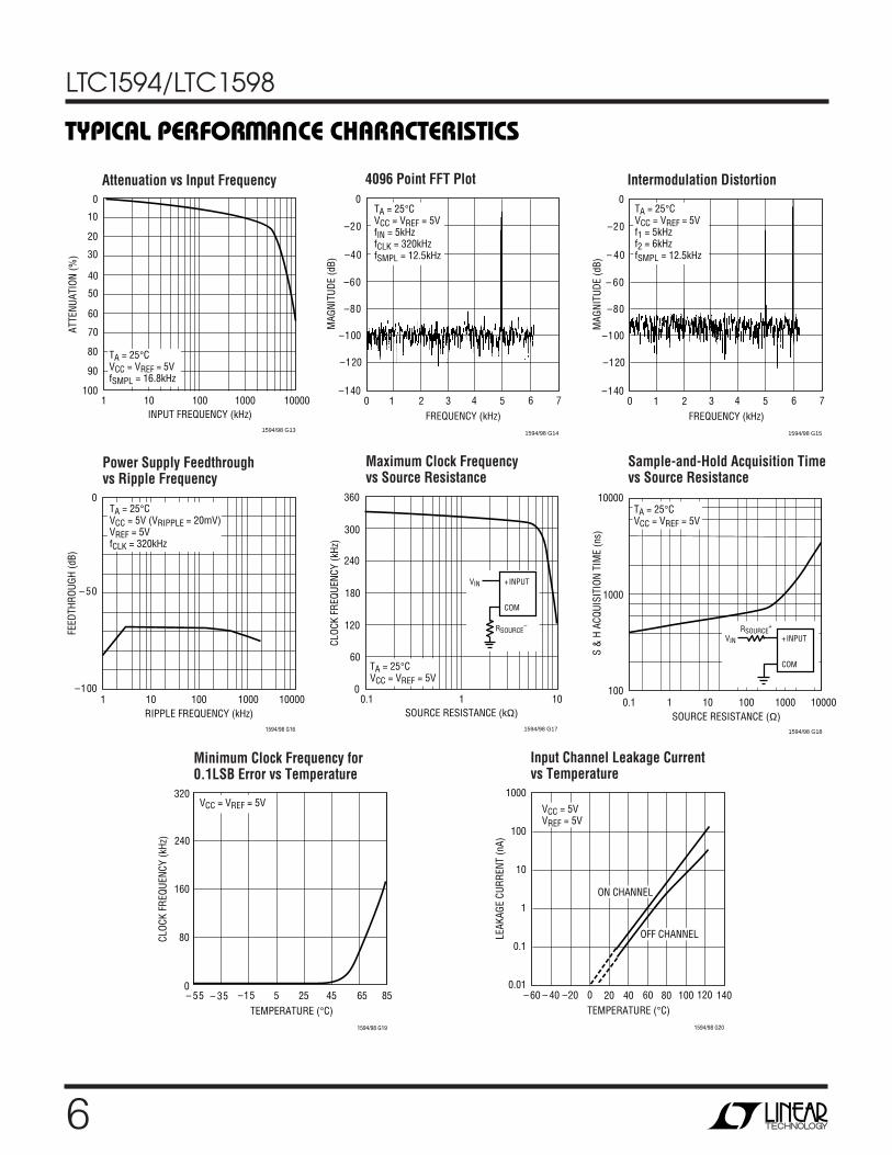
TYPICAL PERFORMANCE CHARACTERISTICS
UW
SAMPLE FREQUENCY (kHz)0.1
1
SUPP
LY C
URRE
NT (µ
A)
10
100
1000
1 10 100
1594/98 G01
TA = 25°CVCC = 5VVREF = 5VfCLK = 320kHz
Supply Current vs Sample Rate
TEMPERATURE (°C)–55
92.0
REFE
RENC
E CU
RREN
T (µ
A)
92.5
93.5
94.0
94.5
–15 25 45 125
1594/98 G03
93.0
–35 5 65 85 105
95.0VCC = VREF = 5VfSMPL = 16.8kHzfCLK = 320kHz
TEMPERATURE (°C)–55
200
SUPP
LY C
URRE
NT (µ
A)
250
350
400
450
–15 25 45 125
1594/98 G02
300
–35 5 65 85 105
TA = 25°CVCC = VREF = 5VfCLK = 320kHzfSMPL = 16.8kHz
Supply Current vs Temperature Reference Current vs Temperature

5
LTC1594/LTC1598
TYPICAL PERFORMANCE CHARACTERISTICS
UW
0
–0.05
–0.15
–0.20
–0.25
–0.30
–0.50
–0.35
–0.10
–0.40
–0.45
REFERENCE VOLTAGE (V)1.0
CHAN
GE IN
LIN
EARI
TY (L
SB)
2.0 3.0 4.0 5.0
1594/98 G06
1.5 2.5 3.5 4.5
TA = 25°CVCC = 5VfCLK = 320kHzfSMPL = 16.8kHz
Change in Linearityvs Reference Voltage
TEMPERATURE (°C)–55
–3.0
CHAN
GE IN
OFF
SET
(LSB
)
–2.5
–2.0
–1.5
–1.0
–15 25 65
1594/98 G05
–0.5
0
–35 5 45 85
VCC = VREF = 5VfCLK = 320kHzfSMPL = 16.8kHz
Change in Offset vs Temperature
Change in Gainvs Reference Voltage
REFERENCE VOLTAGE (V)1.0
0
CHAN
GE IN
OFF
SET
(LSB
= 1
/409
6 V R
EF)
0.5
1.0
1.5
2.0
2.0 3.0 4.0 5.0
1594/98 G04
2.5
3.0
1.5 2.5 3.5 4.5
TA = 25°CVCC = 5VfCLK = 320kHzfSMPL = 16.8kHz
Change in Offsetvs Reference Voltage
0
–1
–3
–4
–5
–6
–10
–7
–2
–8
–9
REFERENCE VOLTAGE (V)1.0
CHAN
GE IN
GAI
N (L
SB)
2.0 3.0 4.0 5.0
1594/98 G07
1.5 2.5 3.5 4.5
TA = 25°CVCC = 5VfCLK = 320kHzfSMPL = 16.8kHz
Peak-to-Peak ADC Noisevs Reference Voltage
REFERENCE VOLTAGE (V)1
ADC
NOIS
E IN
LBS
s
1.0
1.5
5
1594/98 G08
0.5
02 3 4
2.0TA = 25°CVCC = 5VfCLK = 320kHz
Differential Nonlinearity vs Code
Effective Bits and S/(N + D)vs Input Frequency S/(N + D) vs Input Level
INPUT FREQUENCY (kHz)1
0
EFFE
CTIV
E NU
MBE
R OF
BIT
S (E
NOBs
)
87
109
1211
10 100 1000
1594/98 G10
6
5044
6256
7468
385
43
21
TA = 25°CVCC = 5VfCLK = 320kHzfSMPL = 16.8kHz
INPUT LEVEL (dB)– 40
0
SIGN
AL-T
O-NO
ISE
PLUS
DIS
TORT
ION
(dB)
20
10
40
30
60
50
80
70
– 30 –20
1594/98 G12
–10 0
TA = 25°CVCC = VREF = 5VfIN = 1kHzfSMPL = 16.8kHz
Spurious Free Dynamic Rangevs Frequency
INPUT FREQUENCY (kHz)1
40
SPUR
IOUS
FRE
E DY
NAM
IC R
ANGE
(dB
)
50
60
70
80
10 100 1000
1594/98 G11
30
20
10
0
90
100
TA = 25°CVCC = VREF = 5VfSMPL = 16.8kHz
CODE0
DIFF
EREN
TIAL
NON
LINE
ARIT
Y ER
ROR
(LBS
)
–1.0
– 0.8
– 0.6
– 0.4
– 0.2
0.4
0.6
0.8
1.0
0.2
0.0
2048
1594/98 G09
4096
6
LTC1594/LTC1598
TYPICAL PERFORMANCE CHARACTERISTICS
UW
Intermodulation Distortion
FREQUENCY (kHz)0
– 60
– 40
0
3 5
1594/98 G15
–80
–100
1 2 4 6 7
–120
–140
–20
MAG
NITU
DE (d
B)
TA = 25°CVCC = VREF = 5Vf1 = 5kHzf2 = 6kHzfSMPL = 12.5kHz
Attenuation vs Input Frequency 4096 Point FFT Plot
FREQUENCY (kHz)0
–60
–40
0
3 5
1594/98 G14
–80
–100
1 2 4 6 7
–120
–140
–20
MAG
NITU
DE (d
B)
TA = 25°CVCC = VREF = 5VfIN = 5kHzfCLK = 320kHzfSMPL = 12.5kHz
Power Supply Feedthroughvs Ripple Frequency
Maximum Clock Frequencyvs Source Resistance
INPUT FREQUENCY (kHz)1 10
100
ATTE
NUAT
ION
(%)
80
90
60
70
40
50
20
30
100 1000 10000
1594/98 G13
0
10
TA = 25°CVCC = VREF = 5VfSMPL = 16.8kHz
RIPPLE FREQUENCY (kHz)
FEED
THRO
UGH
(dB)
– 50
0
1 100 1000 10000
1594/98 G16
–10010
TA = 25°CVCC = 5V (VRIPPLE = 20mV)VREF = 5VfCLK = 320kHz
SOURCE RESISTANCE (kΩ)0.1
0
CLOC
K FR
EQUE
NCY
(kHz
)
60
120
180
240
360
1 10
1594/98 G17
300
+INPUT
COM
RSOURCE–
VIN
TA = 25°CVCC = VREF = 5V
Sample-and-Hold Acquisition Timevs Source Resistance
SOURCE RESISTANCE (Ω)10 100 1000
1594/98 G18
10.1 10000100
S &
H A
CQUI
SITI
ON T
IME
(ns)
1000
10000TA = 25°CVCC = VREF = 5V
+INPUT
COM
RSOURCE+
VIN
Input Channel Leakage Currentvs Temperature
TEMPERATURE (°C)– 60
LEAK
AGE
CURR
ENT
(nA)
1000
100
10
1
0.1
0.01100
1594/98 G20
–20 20 60 140– 40 0 40 80 120
VCC = 5VVREF = 5V
ON CHANNEL
OFF CHANNEL
Minimum Clock Frequency for0.1LSB Error vs Temperature
TEMPERATURE (°C)– 55
CLOC
K FR
EQUE
NCY
(kHz
)
160
240
25 45 65 85
1594/98 G19
80
0– 35 –15 5
320VCC = VREF = 5V
7
LTC1594/LTC1598
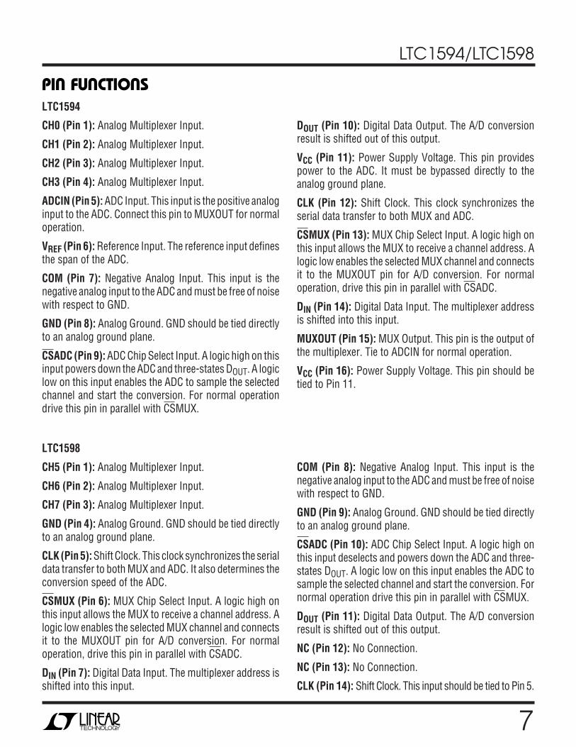
PIN FUNCTIONS
UUU
LTC1594
CH0 (Pin 1): Analog Multiplexer Input.
CH1 (Pin 2): Analog Multiplexer Input.
CH2 (Pin 3): Analog Multiplexer Input.
CH3 (Pin 4): Analog Multiplexer Input.
ADCIN (Pin 5): ADC Input. This input is the positive analoginput to the ADC. Connect this pin to MUXOUT for normaloperation.
VREF (Pin 6): Reference Input. The reference input definesthe span of the ADC.
COM (Pin 7): Negative Analog Input. This input is thenegative analog input to the ADC and must be free of noisewith respect to GND.
GND (Pin 8): Analog Ground. GND should be tied directlyto an analog ground plane.
CSADC (Pin 9): ADC Chip Select Input. A logic high on thisinput powers down the ADC and three-states DOUT. A logiclow on this input enables the ADC to sample the selectedchannel and start the conversion. For normal operationdrive this pin in parallel with CSMUX.
LTC1598
CH5 (Pin 1): Analog Multiplexer Input.
CH6 (Pin 2): Analog Multiplexer Input.
CH7 (Pin 3): Analog Multiplexer Input.
GND (Pin 4): Analog Ground. GND should be tied directlyto an analog ground plane.
CLK (Pin 5): Shift Clock. This clock synchronizes the serialdata transfer to both MUX and ADC. It also determines theconversion speed of the ADC.
CSMUX (Pin 6): MUX Chip Select Input. A logic high onthis input allows the MUX to receive a channel address. Alogic low enables the selected MUX channel and connectsit to the MUXOUT pin for A/D conversion. For normaloperation, drive this pin in parallel with CSADC.
DIN (Pin 7): Digital Data Input. The multiplexer address isshifted into this input.
DOUT (Pin 10): Digital Data Output. The A/D conversionresult is shifted out of this output.
VCC (Pin 11): Power Supply Voltage. This pin providespower to the ADC. It must be bypassed directly to theanalog ground plane.
CLK (Pin 12): Shift Clock. This clock synchronizes theserial data transfer to both MUX and ADC.
CSMUX (Pin 13): MUX Chip Select Input. A logic high onthis input allows the MUX to receive a channel address. Alogic low enables the selected MUX channel and connectsit to the MUXOUT pin for A/D conversion. For normaloperation, drive this pin in parallel with CSADC.
DIN (Pin 14): Digital Data Input. The multiplexer addressis shifted into this input.
MUXOUT (Pin 15): MUX Output. This pin is the output ofthe multiplexer. Tie to ADCIN for normal operation.
VCC (Pin 16): Power Supply Voltage. This pin should betied to Pin 11.
COM (Pin 8): Negative Analog Input. This input is thenegative analog input to the ADC and must be free of noisewith respect to GND.
GND (Pin 9): Analog Ground. GND should be tied directlyto an analog ground plane.
CSADC (Pin 10): ADC Chip Select Input. A logic high onthis input deselects and powers down the ADC and three-states DOUT. A logic low on this input enables the ADC tosample the selected channel and start the conversion. Fornormal operation drive this pin in parallel with CSMUX.
DOUT (Pin 11): Digital Data Output. The A/D conversionresult is shifted out of this output.
NC (Pin 12): No Connection.
NC (Pin 13): No Connection.
CLK (Pin 14): Shift Clock. This input should be tied to Pin 5.

8
LTC1594/LTC1598
PIN FUNCTIONS
UUU
VCC (Pin 15): Power Supply Voltage. This pin providespower to the A/D Converter. It must be bypassed directlyto the analog ground plane.
VREF (Pin 16): Reference Input. The reference input de-fines the span of the ADC.
ADCIN (Pin 17): ADC Input. This input is the positiveanalog input to the ADC. Connect this pin to MUXOUT fornormal operation.
MUXOUT (Pin 18): MUX Output. This pin is the output ofthe multiplexer. Tie to ADCIN for normal operation.
VCC (Pin 19): Power Supply Voltage. This pin should betied to Pin 15.
CH0 (Pin 20): Analog Multiplexer Input.
CH1 (Pin 21): Analog Multiplexer Input.
CH2 (Pin 22): Analog Multiplexer Input.
CH3 (Pin 23): Analog Multiplexer Input.
CH4 (Pin 24): Analog Multiplexer Input.
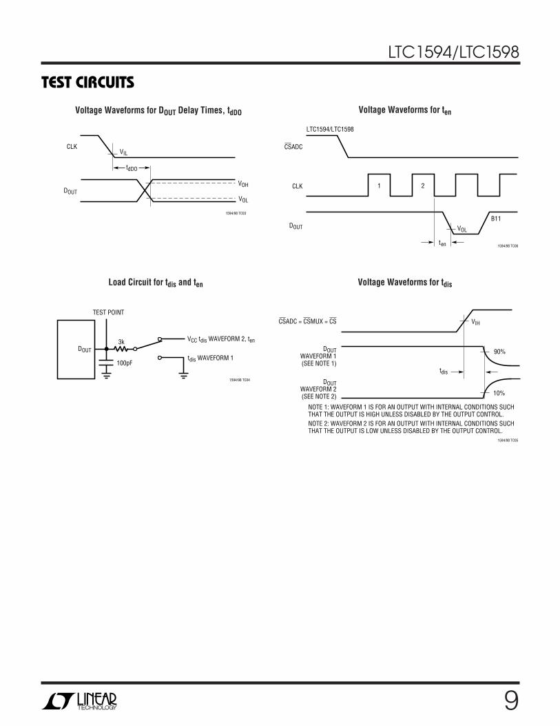
TEST CIRCUITS
Voltage Waveforms for DOUT Rise and Fall Times, tr, tfLoad Circuit for tdDO, tr and tf
DOUT
1.4V
3k
100pF
TEST POINT
1594/98 TC01
DOUTVOL
VOH
tr tf 1594/98 TC02
1594/98 BD
CH0
CH1
CH2
CH3
CH4
CH5
CH6
CH7
20
21
22
23
24
1
2
3
+
–
8-CHANNELMUX
8 COMGND
4, 9
10
6
5, 14
7
11
CSADC
CSMUX
CLK
DIN
DOUT12
13NC
NC
12-BITSAMPLING
ADC
ADCINMUXOUT
18 17 16 15, 19
VREF VCC
CH0
CH1
CH2
CH3
1
2
3
4
+
–
4-CHANNELMUX
7 COMGND
8
9
13
12
14
10
CSADC
CSMUX
CLK
DIN
DOUT
12-BITSAMPLING
ADC
ADCINMUXOUT
15 5 6 16
VREF VCC
LTC1594
LTC1598
BLOCK DIAGRA S
W
LTC1594 LTC1598
9
LTC1594/LTC1598
TEST CIRCUITS
Voltage Waveforms for tenVoltage Waveforms for DOUT Delay Times, tdDO
CLK
DOUT
VIL
tdDO
VOL
VOH
1594/98 TC03
1594/98 TC06
CSADC
LTC1594/LTC1598
1CLK
DOUT
ten
B11VOL
2
DOUTWAVEFORM 1(SEE NOTE 1)
VIH
tdis
90%
10%
DOUTWAVEFORM 2(SEE NOTE 2)
CSADC = CSMUX = CS
NOTE 1: WAVEFORM 1 IS FOR AN OUTPUT WITH INTERNAL CONDITIONS SUCHTHAT THE OUTPUT IS HIGH UNLESS DISABLED BY THE OUTPUT CONTROL.NOTE 2: WAVEFORM 2 IS FOR AN OUTPUT WITH INTERNAL CONDITIONS SUCHTHAT THE OUTPUT IS LOW UNLESS DISABLED BY THE OUTPUT CONTROL.
1594/98 TC05
Load Circuit for tdis and ten
DOUT3k
100pF
TEST POINT
VCC tdis WAVEFORM 2, ten
tdis WAVEFORM 1
1594/98 TC04
Voltage Waveforms for tdis
10
LTC1594/LTC1598
APPLICATIONS INFORMATION
WU UU
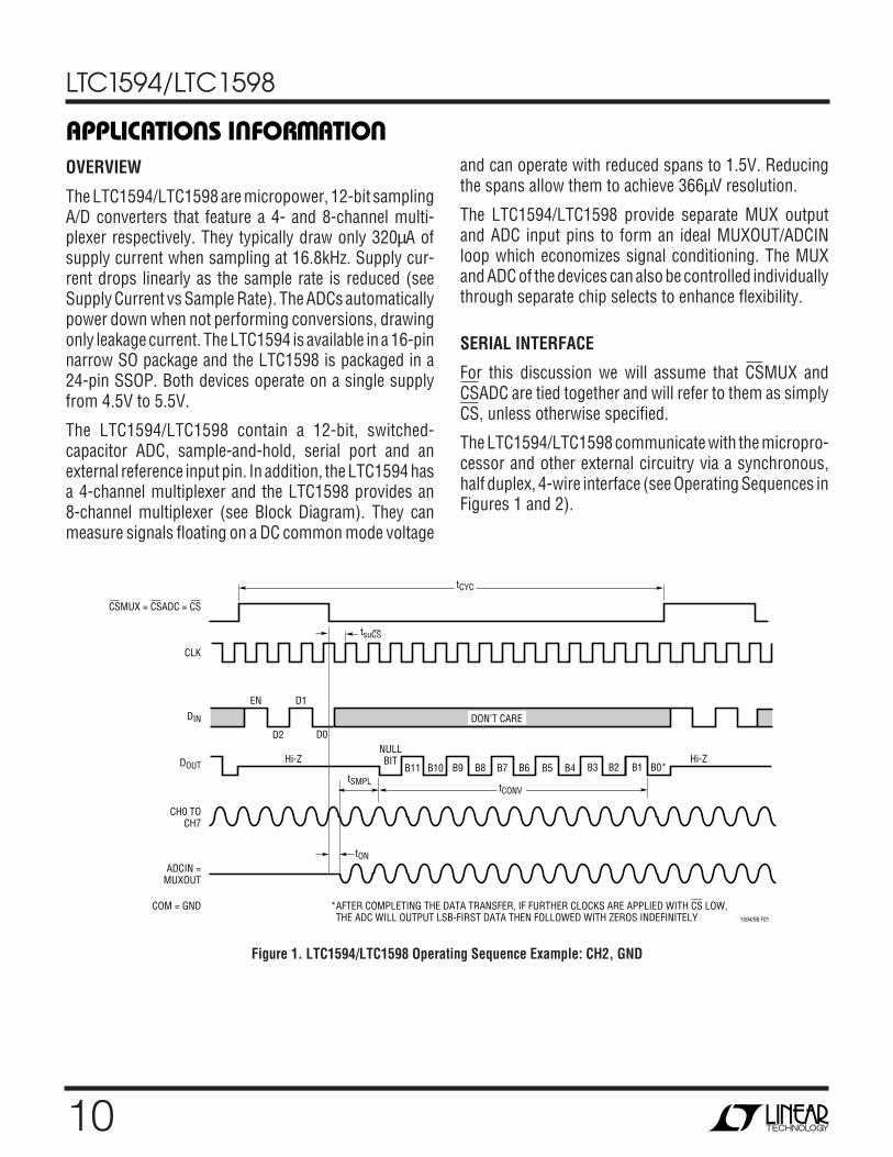
OVERVIEW
The LTC1594/LTC1598 are micropower, 12-bit samplingA/D converters that feature a 4- and 8-channel multi-plexer respectively. They typically draw only 320µA ofsupply current when sampling at 16.8kHz. Supply cur-rent drops linearly as the sample rate is reduced (seeSupply Current vs Sample Rate). The ADCs automaticallypower down when not performing conversions, drawingonly leakage current. The LTC1594 is available in a 16-pinnarrow SO package and the LTC1598 is packaged in a24-pin SSOP. Both devices operate on a single supplyfrom 4.5V to 5.5V.
The LTC1594/LTC1598 contain a 12-bit, switched-capacitor ADC, sample-and-hold, serial port and anexternal reference input pin. In addition, the LTC1594 hasa 4-channel multiplexer and the LTC1598 provides an8-channel multiplexer (see Block Diagram). They canmeasure signals floating on a DC common mode voltage
and can operate with reduced spans to 1.5V. Reducingthe spans allow them to achieve 366µV resolution.
The LTC1594/LTC1598 provide separate MUX outputand ADC input pins to form an ideal MUXOUT/ADCINloop which economizes signal conditioning. The MUXand ADC of the devices can also be controlled individuallythrough separate chip selects to enhance flexibility.
SERIAL INTERFACE
For this discussion we will assume that CSMUX andCSADC are tied together and will refer to them as simplyCS, unless otherwise specified.
The LTC1594/LTC1598 communicate with the micropro-cessor and other external circuitry via a synchronous,half duplex, 4-wire interface (see Operating Sequences inFigures 1 and 2).
CLK
EN D1
D2
CSMUX = CSADC = CS
tCYC
B5B6B7B8B9B10B11Hi-ZDOUT
CH0 TOCH7
DIN
tCONV
Hi-Z
tsuCS
NULLBIT
D0
B4 B3 B2 B1 B0*tSMPL
tON
DON’T CARE
ADCIN =MUXOUT
COM = GND *AFTER COMPLETING THE DATA TRANSFER, IF FURTHER CLOCKS ARE APPLIED WITH CS LOW, THE ADC WILL OUTPUT LSB-FIRST DATA THEN FOLLOWED WITH ZEROS INDEFINITELY 1594/98 F01
Figure 1. LTC1594/LTC1598 Operating Sequence Example: CH2, GND
11
LTC1594/LTC1598
APPLICATIONS INFORMATION
WU UU
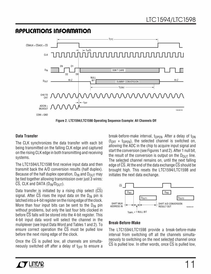
Figure 2. LTC1594/LTC1598 Operating Sequence Example: All Channels Off
CLK
EN D1
D2
tCYC
Hi-ZDOUT
CH0 TOCH7
DIN
tCONV
Hi-Z
tsuCS
NULLBIT
D0
tOFF
D0N‘T CARE
ADCIN =MUXOUT
COM = GND
1594/98 F02
DUMMY CONVERSION
CSMUX = CSADC = CS
break-before-make interval, tOPEN. After a delay of tON(tOFF + tOPEN), the selected channel is switched on,allowing the ADC in the chip to acquire input signal andstart the conversion (see Figures 1 and 2). After 1 null bit,the result of the conversion is output on the DOUT line.The selected channel remains on, until the next fallingedge of CS. At the end of the data exchange CS should bebrought high. This resets the LTC1594/LTC1598 andinitiates the next data exchange.
DIN1 DIN2
DOUT1 DOUT2
CS
SHIFT MUXADDRESS IN
tSMPL + 1 NULL BIT
SHIFT A/D CONVERSIONRESULT OUT 1594/98 AI01
Break-Before-Make
The LTC1594/LTC1598 provide a break-before-makeinterval from switching off all the channels simulta-neously to switching on the next selected channel onceCS is pulled low. In other words, once CS is pulled low,
Data Transfer
The CLK synchronizes the data transfer with each bitbeing transmitted on the falling CLK edge and capturedon the rising CLK edge in both transmitting and receivingsystems.
The LTC1594/LTC1598 first receive input data and thentransmit back the A/D conversion results (half duplex).Because of the half duplex operation, DIN and DOUT maybe tied together allowing transmission over just 3 wires:CS, CLK and DATA (DIN/DOUT).
Data transfer is initiated by a rising chip select (CS)signal. After CS rises the input data on the DIN pin islatched into a 4-bit register on the rising edge of the clock.More than four input bits can be sent to the DIN pinwithout problems, but only the last four bits clocked inbefore CS falls will be stored into the 4-bit register. This4-bit input data word will select the channel in themuliplexer (see Input Data Word and Tables 1 and 2). Toensure correct operation the CS must be pulled lowbefore the next rising edge of the clock.
Once the CS is pulled low, all channels are simulta-neously switched off after a delay of tOFF to ensure a

12
LTC1594/LTC1598
after a delay of tOFF, all the channels are switched off toensure a break-before-make interval. After this interval,the selected channel is switched on allowing signaltransmission. The selected channel remains on until thenext falling edge of CS and the process repeats itself withthe “EN” bit being logic high. If the “EN” bit is logic low,all the channels are switched off simultaneously after adelay of tOFF from CS being pulled low and all thechannels remain off until the next falling edge of CS.
Input Data Word
When CS is high, the LTC1594/LTC1598 clock data intothe DIN inputs on the rising edge of the clock and store thedata into a 4-bit register. The input data words are definedas follows:
D0EN D2 D1
CHANNEL SELECTION1594/98 AI02
“EN” Bit
The first bit in the 4-bit register is an “EN” bit. If the “EN”bit is a logic high, as illustrated in Figure 1, it enables theselected channel after a delay of tON when the CS is pulledlow. If the “EN” bit is logic low, as illustrated in Figure 2,it disables all channels after a delay of tOFF when the CSis pulled low.
Multiplexer (MUX) Address
The 3 bits of input word following the “EN” bit select thechannel in the MUX for the requested conversion. For agiven channel selection, the converter will measure thevoltage of the selected channel with respect to the voltageon the COM pin. Tables 1 and 2 show the various bitcombinations for the LTC1594/LTC1598 channel selection.
Table 1. Logic Table for the LTC1594 Channel SelectionCHANNEL STATUS EN D2 D1 DO
All Off 0 X X X
CH0 1 0 0 0
CH1 1 0 0 1
CH2 1 0 1 0
CH3 1 0 1 1
APPLICATIONS INFORMATION
WU UU
Table 2. Logic Table for the LTC1598 Channel SelectionCHANNEL STATUS EN D2 D1 DO
All Off 0 X X X
CH0 1 0 0 0
CH1 1 0 0 1
CH2 1 0 1 0
CH3 1 0 1 1
CH4 1 1 0 0
CH5 1 1 0 1
CH6 1 1 1 0
CH7 1 1 1 1
Transfer Curve
The LTC1594/LTC1598 are permanently configured forunipolar only. The input span and code assignment forthis conversion type is illustrated below.
Transfer Curve
0V 1LSB
VREF –2LSB
VREF4096
VREF –1LSB
VREF
VIN 0 0 0 0 0 0 0 0 0 0 0 1
0 0 0 0 0 0 0 0 0 0 0 0
1 1 1 1 1 1 1 1 1 1 1 1
1 1 1 1 1 1 1 1 1 1 1 0
•••
1594/98 • AI03
1LSB =
Output Code
OUTPUT CODE
•••
1 1 1 1 1 1 1 1 1 1 1 1 1 1 1 1 1 1 1 1 1 1 1 1 1 1 1 0
0 0 0 0 0 0 0 0 0 0 0 0 0 1 0 0 0 0 0 0 0 0 0 0 0 0 0 0
INPUT VOLTAGE
VREF – 1LSBVREF – 2LSB
•••
1LSB0V
INPUT VOLTAGE(VREF = 5.000V)
4.99878V4.99756V
•••
0.00122V0V
1594/98 • AI04

13
LTC1594/LTC1598
APPLICATIONS INFORMATION
WU UU
Operation with DIN and DOUT Tied Together
The LTC1594/LTC1598 can be operated with DIN andDOUT tied together. This eliminates one of the linesrequired to communicate to the microprocessor (MPU).Data is transmitted in both directions on a single wire.The processor pin connected to this data line should beconfigurable as either an input or an output. The LTC1594/LTC1598 will take control of the data line after CS fallingand before the 6th falling CLK while the processor takescontrol of the data line when CS is high (see Figure 3).
Therefore the processor port line must be switched to aninput with CS being low to avoid a conflict.
Separate Chip Selects for MUX and ADC
The LTC1594/LTC1598 provide separate chip selects,CSMUX and CSADC, to control MUX and ADC separately.This feature not only provides the flexibility to select aparticular channel once for multiple conversions (seeFigure 4) but also maximizes the sample rate up to20ksps (see Figure 5).
Figure 4. Select Certain Channel Once for Mulitple Conversions
CLK
EN D1
D2
CSADC
CSMUX
B5B6B7B8B9B10B11Hi-ZDOUT
CH0 TOCH7
DIN
tCONV
Hi-Z
tsuCS
NULLBIT
D0
B4 B3 B2 B1 B0tSMPL
tON
B5B6B7B8B9B10B11Hi-Z
tCONV
tsuCS
NULLBIT
D0
B4 B3 B2 B1 B0tSMPL
ADCIN =MUXOUT
COM = GND1594 TD01
DON’T CARE DON’T CARE
1 2 3 4 5 6
CS
CLK
DATA (DIN/DOUT) EN D2 D1 D0 B11 B10 • • •
LTC1594/LTC1598 CONTROLS DATA LINE AND SENDSA/D RESULT BACK TO MPU
MPU CONTROLS DATA LINE AND SENDSMUX ADDRESS TO LTC1594/LTC1598
PROCESSOR MUST RELEASE DATALINE AFTER CS FALLING AND
BEFORE THE 6TH FALLING CLK
LTC1594/LTC1598 TAKES CONTROL OF DATALINE AFTER CS FALLING AND BEFORE THE 6TH FALLING CLK 1594/98 F03
tsuCS
Figure 3. LTC1594/LTC1598 Operation with DIN and DOUT Tied Together

14
LTC1594/LTC1598
APPLICATIONS INFORMATION
WU UU
CLK
EN D1
D2
CSMUX
CSADC
B5B6B7B8B9B10B11DOUT
CH0 TOCH7
DIN
tCONV
tsuCS
NULLBIT
D0
B4 B3 B2 B1 B0
EN D1
tSMPL
tON tON
B5B6B7B8B9B10B11
tCONV
tsuCS
NULLBIT
D0D2
EN D1
D0D2
B4 B3 B2 B1 B0tSMPL
ADCIN =MUXOUT
COM = GND1594/98 F05
B4 B3 B2 B1 B0
DON’T CARE DON’T CARE
MUXOUT/ADCIN Loop EconomizesSignal Conditioning
The MUXOUT and ADCIN pins of the LTC1594/LTC1598form a very flexible external loop that allows Program-mable Gain Amplifier (PGA) and/or processing analoginput signals prior to conversion. This loop is also a costeffective way to perform the conditioning, because onlyone circuit is needed instead of one for each channel.
In the Typical Applications section, there are a fewexamples illustrating how to use the MUXOUT/ADCIN loopto form a PGA and to antialias filter several analog inputs.
ACHIEVING MICROPOWER PERFORMANCE
With typical operating currents of 320µA and automaticshutdown between conversions, the LTC1594/LTC1598achieve extremely low power consumption over a widerange of sample rates (see Figure 6). The auto shutdownallows the supply current to drop with reduced samplerate. Several things must be taken into account to achievesuch a low power consumption.
Shutdown
The LTC1594/LTC1598 are equipped with automatic shut-down features. They draw power when the CS pin is low.The bias circuits and comparator of the ADC powers downand the reference input becomes high impedance at theend of each conversion leaving the CLK running to clockout the LSB first data or zeroes (see Figures 1 and 2). Whenthe CS pin is high, the ADC powers down completely
leaving the CLK running to clock the input data word intoMUX. If the CS, DIN and CLK are not running rail-to-rail, theinput logic buffers will draw currents. These currents maybe large compared to the typical supply current. To obtainthe lowest supply current, run the CS, DIN and CLK pinsrail-to-rail.
DOUT Loading
Capacitive loading on the digital output can increasepower consumption. A 100pF capacitor on the DOUT pincan add more than 80mA to the supply current at a320kHz clock frequency. An extra 80mA or so of currentgoes into charging and discharging the load capacitor.The same goes for digital lines driven at a high frequencyby any logic. The (C)(V)(f) currents must be evaluatedand the troublesome ones minimized.
Figure 5. Use Separate Chip Selects to Maximize Sample Rate
SAMPLE FREQUENCY (kHz)0.1
1
SUPP
LY C
URRE
NT (µ
A)
10
100
1000
1 10 100
1594/98 F06
TA = 25°CVCC = 5VVREF = 5VfCLK = 320kHz
Figure 6. Automatic Power Shutdown Between ConversionsAllows Power Consumption to Drop with Sample Rate
15
LTC1594/LTC1598
APPLICATIONS INFORMATION
WU UU
BOARD LAYOUT CONSIDERATIONS
Grounding and Bypassing
The LTC1594/LTC1598 are easy to use if some care istaken. They should be used with an analog ground planeand single point grounding techniques. The GND pinshould be tied directly to the ground plane.
The VCC pin should be bypassed to the ground plane witha 10µF tantalum capacitor with leads as short as possible.If the power supply is clean, the LTC1594/LTC1598 canalso operate with smaller 1µF or less surface mount orceramic bypass capacitors. All analog inputs should bereferenced directly to the single point ground. Digitalinputs and outputs should be shielded from and/orrouted away from the reference and analog circuitry.
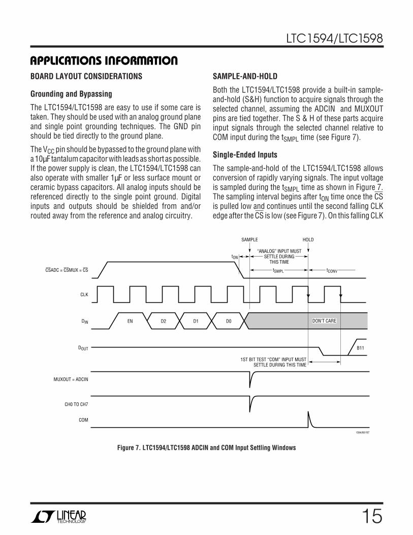
SAMPLE-AND-HOLD
Both the LTC1594/LTC1598 provide a built-in sample-and-hold (S&H) function to acquire signals through theselected channel, assuming the ADCIN and MUXOUTpins are tied together. The S & H of these parts acquireinput signals through the selected channel relative toCOM input during the tSMPL time (see Figure 7).
Single-Ended Inputs
The sample-and-hold of the LTC1594/LTC1598 allowsconversion of rapidly varying signals. The input voltageis sampled during the tSMPL time as shown in Figure 7.The sampling interval begins after tON time once the CSis pulled low and continues until the second falling CLKedge after the CS is low (see Figure 7). On this falling CLK
Figure 7. LTC1594/LTC1598 ADCIN and COM Input Settling Windows
CLK
DIN
DOUT
MUXOUT = ADCIN
CH0 TO CH7
SAMPLE HOLD
“ANALOG” INPUT MUSTSETTLE DURING
THIS TIME
tSMPL
tON
tCONVCSADC = CSMUX = CS
D2 D1EN D0 DON‘T CARE
1ST BIT TEST “COM” INPUT MUSTSETTLE DURING THIS TIME
B11
COM
1594/98 F07

16
LTC1594/LTC1598
APPLICATIONS INFORMATION
WU UU
edge, the S & H goes into hold mode and the conversionbegins. The voltage on the “COM” input must remainconstant and be free of noise and ripple throughout theconversion time. Otherwise, the conversion operationmay not be performed accurately. The conversion time is12 CLK cycles. Therefore, a change in the “COM” inputvoltage during this interval can cause conversion errors.For a sinusoidal voltage on the “COM” input this errorwould be:
VERROR(MAX) = VPEAK(2π)(f)(“COM”)12/fCLK
Where f(“COM”) is the frequency of the “COM” inputvoltage, VPEAK is its peak amplitude and fCLK is thefrequency of the CLK. In most cases VERROR will not besignificant. For a 60Hz signal on the “COM” input togenerate a 1/4LSB error (305µV) with the converterrunning at CLK = 320kHz, its peak value would have to be8.425mV.
ANALOG INPUTS
Because of the capacitive redistribution A/D conversiontechniques used, the analog inputs of the LTC1594/LTC1598 have capacitive switching input current spikes.These current spikes settle quickly and do not cause aproblem. However, if large source resistances are usedor if slow settling op amps drive the inputs, care must betaken to insure that the transients caused by the currentspikes settle completely before the conversion begins.
“Analog” Input Settling
The input capacitor of the LTC1594/LTC1598 is switchedonto the selected channel input during the tSMPL time (seeFigure 7) and samples the input signal within that time. Thesample phase is at least 1 1/2 CLK cycles before conver-sion starts. The voltage on the “analog” input must settlecompletely within tSMPL. Minimizing RSOURCE
+ and C1 willimprove the input settling time. If a large “analog” inputsource resistance must be used, the sample time can beincreased by using a slower CLK frequency.
“COM” Input Settling
At the end of the tSMPL, the input capacitor switches to the“COM” input and conversion starts (see Figures 1 and 7).
During the conversion, the “analog” input voltage iseffectively “held” by the sample-and-hold and will notaffect the conversion result. However, it is critical that the“COM” input voltage settles completely during the firstCLK cycle of the conversion time and be free of noise.Minimizing RSOURCE
– and C2 will improve settling time.If a large “COM” input source resistance must be used,the time allowed for settling can be extended by using aslower CLK frequency.
Input Op Amps
When driving the analog inputs with an op amp it isimportant that the op amp settle within the allowed time(see Figure 7). Again, the “analog” and “COM” inputsampling times can be extended as described above toaccommodate slower op amps. Most op amps, includingthe LT®1006 and LT1413 single supply op amps, can bemade to settle well even with the minimum settlingwindows of 4.8µs (“analog” input) which occur at themaximum clock rate of 320kHz.
Source Resistance
The analog inputs of the LTC1594/LTC1598 look like a20pF capacitor (CIN) in series with a 500Ω resistor (RON)and a 45Ω channel resistance as shown in Figure 8.CIN gets switched between the selected “analog” and“COM” inputs once during each conversion cycle. Largeexternal source resistors and capacitances will slow thesettling of the inputs. It is important that the overall RCtime constants be short enough to allow the analoginputs to completely settle within the allowed time.
Figure 8. Analog Input Equivalent Circuit
RON500Ω
RON45Ω
CIN20pF
LTC1594LTC1598
“ANALOG”INPUTRSOURCE+
VIN+
C1
“COM”INPUT
MUXOUT
MUX
ADCIN
RSOURCE–VIN–
C2 1594/98 • F08

17
LTC1594/LTC1598
Input Leakage Current
Input leakage currents can also create errors if the sourceresistance gets too large. For instance, the maximuminput leakage specification of 200nA (at 85°C) flowingthrough a source resistance of 1.2k will cause a voltagedrop of 240µV or 0.2LSB. This error will be muchreduced at lower temperatures because leakage dropsrapidly (see typical curve Input Channel Leakage Currentvs Temperature).
REFERENCE INPUTS
The reference input of the LTC1594/LTC1598 is effec-tively a 50k resistor from the time CS goes low to the endof the conversion. The reference input becomes a highimpedance node at any other time (see Figure 9). Sincethe voltage on the reference input defines the voltagespan of the A/D converter, the reference input should bedriven by a reference with low ROUT (ex. LT1004, LT1019and LT1021) or a voltage source with low ROUT.
Reduced Reference Operation
The effective resolution of the LTC1594/LTC1598 can beincreased by reducing the input span of the converters.The LTC1594/LTC1598 exhibit good linearity and gainover a wide range of reference voltages (see typicalcurves Change in Linearity vs Reference Voltage andChange in Gain vs Reference Voltage). However, caremust be taken when operating at low values of VREFbecause of the reduced LSB step size and the resultinghigher accuracy requirement placed on the converters.The following factors must be considered when operat-ing at low VREF values:
1. Offset2. Noise3. Conversion speed (CLK frequency)
Offset with Reduced VREF
The offset of the LTC1594/LTC1598 has a larger effect onthe output code when the ADCs are operated withreduced reference voltage. The offset (which is typicallya fixed voltage) becomes a larger fraction of an LSB as thesize of the LSB is reduced. The typical curve of Change inOffset vs Reference Voltage shows how offset in LSBs isrelated to reference voltage for a typical value of VOS. Forexample, a VOS of 122µV which is 0.1LSB with a 5Vreference becomes 0.5LSB with a 1V reference and2.5LSBs with a 0.2V reference. If this offset is unaccept-able, it can be corrected digitally by the receiving systemor by offsetting the “COM” input of the LTC1594/LTC1598.
Noise with Reduced VREF
The total input referred noise of the LTC1594/LTC1598can be reduced to approximately 400µV peak-to-peakusing a ground plane, good bypassing, good layouttechniques and minimizing noise on the reference inputs.This noise is insignificant with a 5V reference but willbecome a larger fraction of an LSB as the size of the LSBis reduced.
For operation with a 5V reference, the 400µV noise is only0.33LSB peak-to-peak. In this case, the LTC1594/LTC1598noise will contribute virtually no uncertainty to the outputcode. However, for reduced references the noise maybecome a significant fraction of an LSB and causeundesirable jitter in the output code. For example, with a2.5V reference this same 400µV noise is 0.66LSB peak-to-peak. This will reduce the range of input voltages overwhich a stable output code can be achieved by 1LSB. Ifthe reference is further reduced to 1V, the 400µV noisebecomes equal to 1.65LSBs and a stable code may bedifficult to achieve. In this case averaging multiple read-ings may be necessary.
This noise data was taken in a very clean setup. Any setupinduced noise (noise or ripple on VCC, VREF or VIN) willadd to the internal noise. The lower the reference voltageto be used the more critical it becomes to have a clean,noise free setup.
LTC1594LTC1598
REF+
ROUT
VREF
1
4GND
1594/98 F09
Figure 9. Reference Input Equivalent Circuit
APPLICATIONS INFORMATION
WU UU

18
LTC1594/LTC1598
Conversion Speed with Reduced VREF
With reduced reference voltages, the LSB step size isreduced and the LTC1594/LTC1598 internal comparatoroverdrive is reduced. Therefore, it may be necessary toreduce the maximum CLK frequency when low values ofVREF are used.
DYNAMIC PERFORMANCE
The LTC1594/LTC1598 have exceptional sampling capa-bility. Fast Fourier Transform (FFT) test techniques areused to characterize the ADC’s frequency response,distortion and noise at the rated throughput. By applyinga low distortion sine wave and analyzing the digitaloutput using an FFT algorithm, the ADC’s spectral con-tent can be examined for frequencies outside the funda-mental. Figure 10 shows a typical LTC1594/LTC1598plot.
APPLICATIONS INFORMATION
WU UU
Effective Number of Bits
The Effective Number of Bits (ENOBs) is a measurement ofthe resolution of an ADC and is directly related to S/(N + D)by the equation:
ENOB = [S/(N + D) – 1.76]/6.02
where S/(N + D) is expressed in dB. At the maximumsampling rate of 16.8kHz with a 5V supply, the LTC1594/LTC1598 maintain above 11 ENOBs at 10kHz inputfrequency. Above 10kHz the ENOBs gradually decline, asshown in Figure 11, due to increasing second harmonicdistortion. The noise floor remains low.
FREQUENCY (kHz)0
–60
–40
0
3 5
1594/98 G14
–80
–100
1 2 4 6 7
–120
–140
–20
MAG
NITU
DE (d
B)
TA = 25°CVCC = VREF = 5VfIN = 5kHzfCLK = 320kHzfSMPL = 12.5kHz
Figure 10. LTC1594/LTC1598 Nonaveraged, 4096 Point FFT Plot
INPUT FREQUENCY (kHz)1
0
EFFE
CTIV
E NU
MBE
R OF
BIT
S (E
NOBs
)
87
109
1211
10 100 1000
1594/98 G10
6
5044
6256
7468
385
43
21
TA = 25°CVCC = 5VfCLK = 320kHzfSMPL = 16.8kHz
Figure 11. Effective Bits and S/(N + D) vs Input Frequency
Total Harmonic Distortion
Total Harmonic Distortion (THD) is the ratio of the RMSsum of all harmonics of the input signal to the fundamen-tal itself. The out-of-band harmonics alias into the fre-quency band between DC and half of the samplingfrequency. THD is defined as:
THD =+ + + +
20logV V V V
V22
32
42
N2
1
...
where V1 is the RMS amplitude of the fundamentalfrequency and V2 through VN are the amplitudes of thesecond through the Nth harmonics. The typical THD
Signal-to-Noise Ratio
The Signal-to-Noise plus Distortion Ratio (S/N + D) is theratio between the RMS amplitude of the fundamentalinput frequency to the RMS amplitude of all other fre-quency components at the ADC’s output. The output isband limited to frequencies above DC and below one halfthe sampling frequency. Figure 11 shows a typical spec-tral content with a 16.8kHz sampling rate.
19
LTC1594/LTC1598
specification in the Dynamic Accuracy table includes the2nd through 5th harmonics. With a 7kHz input signal, theLTC1594/LTC1598 have typical THD of 80dB with VCC = 5V.
Intermodulation Distortion
If the ADC input signal consists of more than onespectral component, the ADC transfer function nonlin-earity can produce intermodulation distortion (IMD)in addition to THD. IMD is the change in one sinusoi-dal input caused by the presence of another sinusoidalinput at a different frequency.
If two pure sine waves of frequencies fa and fb are appliedto the ADC input, nonlinearities in the ADC transferfunction can create distortion products at sum anddifference frequencies of mfa ± nfb, where m and n = 0,1, 2, 3, etc. For example, the 2nd order IMD terms include(fa + fb) and (fa – fb) while 3rd order IMD terms include(2fa + fb), (2fa – fb), (fa + 2fb), and (fa – 2fb). If the two inputsine waves are equal in magnitudes, the value (in dB) ofthe 2nd order IMD products can be expressed by thefollowing formula:
IMD f fmplitude f f
a ba b
±( ) =±( )
20loga
amplitude at fa
APPLICATIONS INFORMATION
WU UU
For input frequencies of 5kHz and 6kHz, the IMD of theLTC1594/LTC1598 is 73dB with a 5V supply.
Peak Harmonic or Spurious Noise
The peak harmonic or spurious noise is the largestspectral component excluding the input signal and DC.This value is expressed in dBs relative to the RMS valueof a full-scale input signal.
Full-Power and Full-Linear Bandwidth
The full-power bandwidth is that input frequency at whichthe amplitude of the reconstructed fundamental is re-duced by 3dB for a full-scale input.
The full-linear bandwidth is the input frequency at whichthe effective bits rating of the ADC falls to 11 bits. Beyondthis frequency, distortion of the sampled input signalincreases. The LTC1594/LTC1598 have been designed tooptimize input bandwidth, allowing the ADCs toundersample input signals with frequencies above theconverters’ Nyquist Frequency.
TYPICAL APPLICATIONS N
U
Microprocessor Interfaces
The LTC1594/LTC1598 can interface directly (withoutexternal hardware) to most popular microprocessors’(MPU) synchronous serial formats includingMICROWIRE, SPI and QSPI. If an MPU without a dedi-cated serial port is used, then three of the MPU’s parallelport lines can be programmed to form the serial link to theLTC1594/LTC1598. Included here is one serial interfaceexample.
Motorola SPI (MC68HC05)
The MC68HC05 has been chosen as an example of an MPUwith a dedicated serial port. This MPU transfers data MSB-first and in 8-bit increments. The DIN word sent to the dataregister starts the SPI process. With three8-bit transfers the A/D result is read into the MPU. Thesecond 8-bit transfer clocks B11 through B7 of the A/Dconversion result into the processor. The third 8-bit trans-fer clocks the remaining bits B6 through B0 into the MPU.ANDing the second byte with 1FHEX clears the three mostsignificant bits and ANDing the third byte with FEHEX clearsthe least significant bit. Shifting the data to the right by onebit results in a right justified word.
20
LTC1594/LTC1598
TYPICAL APPLICATIONS N
U
LDA #$52 Configuration data for serial peripheralcontrol register (Interrupts disabled, outputenabled, master, Norm = 0, Ph = 0, Clk/16)
STA $0A Load configuration data into location $0A (SPCR)LDA #$FF Configuration data for I/O ports
(all bits are set as outputs)STA $04 Load configuration data into Port A DDR ($04)STA $05 Load configuration data into Port B DDR ($05)STA $06 Load configuration data into Port C DDR ($06)LDA #$08 Put DIN word for LTC1598 into Accumulator
(CH0 with respect to GND)STA $50 Load DIN word into memory location $50
START BSET 0,$02 Bit 0 Port C ($02) goes high (CS goes high)LDA $50 Load DIN word at $50 into AccumulatorSTA $0C Load DIN word into SPI data register ($0C) and
start clocking dataLOOP1 TST $0B Test status of SPIF bit in SPI status register ($0B)
MC68HC05 CODEBPL LOOP1 Loop if not done with transfer to previous instructionBCLR 0,$02 Bit 0 Port C ($02) goes low (CS goes low)LDA $0C Load contents of SPI data register into AccumulatorSTA $0C Start next SPI cycle
LOOP2 TST $0B Test status of SPIFBPL LOOP2 Loop if not doneLDA $0C Load contents of SPI data register into AccumulatorSTA $0C Start next SPI cycleAND #$IF Clear 3 MSBs of first DOUT wordSTA $00 Load Port A ($00) with MSBs
LOOP3 TST $0B Test status of SPIFBPL LOOP3 Loop if not doneLDA $0C Load contents of SPI data register into AccumulatorAND #$FE Clear LSB of second DOUT wordSTA $01 Load Port B ($01) with LSBsJMP START Go back to start and repeat program
1594/98 TA04
DOUT FROM LTC1598 STORED IN MC68HC05 RAM
B1 B0 0B2B3B5B6 B4
00
LSB
MSB
#00
#01
0 B11 B10 B9 B8 B7
CLK
DIN
CSMUX
CSADCANALOGINPUTS
C0
SCK
MC68HC05
DOUT
MOSI
LTC1598
BYTE 1
BYTE 2 MISO
Hardware and Software Interface to Motorola MC68HC05
Data Exchange Between LTC1598 and MC68HC05
CSMUX= CSADC
= CS
CLK
DOUT
MPURECEIVED
WORD1594/98 TA03
B3B7 B6 B5 B4 B2 B1 B0 B1 B2B11 B10 B9 B8
DIN
MPUTRANSMIT
WORDBYTE 3 BYTE 2
EN D20 D1 XD0
BYTE 1
XX X X X XX0 0 0 X X XX X X XX
BYTE 3BYTE 2BYTE 1
B10? ? 0 B11 B9 B7B8 B6 B5 B3B4 B2 B1 B1B0
DON‘T CARED1D2
?? ? ??? ? ?
DOEN

21
LTC1594/LTC1598
TYPICAL APPLICATIONS N
U
MULTICHANNEL A/D USES A SINGLE ANTIALIASINGFILTER
This circuit demonstrates how the LTC1598’s indepen-dent analog multiplexer can simplify design of a 12-bitdata acquisition system. All eight channels are MUXed intoa single 1kHz, 4th order Sallen-Key antialiasing filter,which is designed for single supply operation. Since theLTC1598’s data converter accepts inputs from ground tothe positive supply, rail-to-rail op amps were chosen forthe filter to maximize dynamic range. The LT1368 dual rail-to-rail op amp is designed to operate with 0.1µF loadcapacitors (C1 and C2). These capacitors provide fre-quency compensation for the amplifiers and help reducethe amplifier’s output impedance and improve supplyrejection at high frequencies. The filter contributes less
than 1LSB of error due to offsets and bias currents. Thefilter’s noise and distortion are less than –72dB for a100Hz, 2VP-P offset sine input.
The combined MUX and A/D errors result in an integralnonlinearity error of ±3LSB (maximum) and a differentialnonlinearity error of ±3/4LSB (maximum). The typicalsignal-to-noise plus distortion ratio is 71dB, with approxi-mately –78dB of total harmonic distortion. The LTC1598is programmed through a 4-wire serial interface that iscompatable with MICROWIRE, SPI and QSPI. Maximumserial clock speed is 320kHz, which corresponds to a16.8kHz sampling rate.
The complete circuit consumes approximately 800µAfrom a single 5V supply.
Simple Data Acquisition System Takes Advantage of the LTC1598’sMUXOUT/ADCIN Pins-to-Filter Analog Signals Prior to A/D Conversion
1
2
3
4
5
6
7
8
9
10
11
12
24
23
22
21
20
19
18
17
16
15
14
13
CH5
CH6
CH7
GND
CLK
CSMUX
DIN
COM
GND
CSADC
DOUT
NC
CH4
CH3
CH2
CH1
CH0
VCC
MUXOUT
ADCIN
VREF
VCC
CLK
NC
LTC1598
ANALOG INPUTS0V TO 5V
RANGE
7.5k 7.5k
1µF
5V
1594/98 TA05DATA INCHIP SELECTCLOCK
DATA OUT
–
+
1µF0.015µF
0.03µFC20.1µF
7.5k 7.5k
0.03µF
0.015µF
–
+
C10.1µF
5V
1/2LT1368
1/2LT1368

22
LTC1594/LTC1598
TYPICAL APPLICATIONS N
U
Using MUXOUT/ADCIN Loop as PGA
This figure shows the LTC1598’s MUXOUT/ADCIN loopand an LT1368 being used to create a single channel PGAwith eight noninverting gains. Combined with the LTC1391,the system can expand to eight channels and eight gainsfor each channel. Using the LTC1594, the PGA is reducedto four gains. The output of the LT1368 drives the ADCINand the resistor ladder. The resistors above the selectedMUX channel form the feedback for the LT1368. The loopgain for this amplifier is RS1/RS2 + 1. RS1 is the summationof the resistors above the selected MUX channel and RS2
Using the MUXOUT/ADCIN Loop of the LTC1598 to Form a PGA with Eight Gains in a Noninverting Configuration
1594/98 TA06
CH0
CH1
CH2
CH3
CH4
CH5
CH6
CH7
20
21
22
23
24
1
2
3
64R
32R
16R
8R
4R
2R
R
R
+
–
8 COM18 MUXOUT
GND
4, 9
10
6
5, 14
11
7
CSADC
CSMUX
CLK
DOUT
DIN
12
13NC
NC
12-BITSAMPLING
ADC
8-CHANNELMUX
1
2
3
4
5
6
7
8
16
15
14
13
12
11
10
9
LTC1391
5V
1µF
ADCIN17 16 15, 19 1µF
0.1µF
5V
1µF
5V
VREF VCC
–
+CH0
CH1
CH2
CH3
CH4
CH5
CH6
CH7
V+
D
V–
DOUT
DIN
CS
CLK
GND
1/2 LT1368
LTC1598
µP/µC
is the summation of the resistors below the selected MUXchannel. If CH0 is selected, the loop gain is 1 since RS1 is0. Table 1 shows the gain for each MUX channel. TheLT1368 dual rail-to-rail op amp is designed to operate with0.1µF load capacitors. These capacitors provide frequencycompensation for the amplifiers, help reduce the amplifi-ers’ output impedance and improve supply rejection athigh frequencies. Because the LT1368’s IB is low, the RONof the selected channel will not affect the loop gain givenby the formula above.

23
LTC1594/LTC1598
G Package24-Lead Plastic SSOP (0.209)
(LTC DWG # 05-08-1640)
Dimensions in inches (millimeters) unless otherwise noted.PACKAGE DESCRIPTION
U0.016 – 0.0500.406 – 1.270
0.010 – 0.020(0.254 – 0.508)
× 45°
0° – 8° TYP0.008 – 0.010
(0.203 – 0.254)
1 2 3 4 5 6 7 8
0.150 – 0.157**(3.810 – 3.988)
16 15 14 13
0.386 – 0.394*(9.804 – 10.008)
0.228 – 0.244(5.791 – 6.197)
12 11 10 9
S16 0695
0.053 – 0.069(1.346 – 1.752)
0.014 – 0.019(0.355 – 0.483)
0.004 – 0.010(0.101 – 0.254)
0.050(1.270)
TYPDIMENSION DOES NOT INCLUDE MOLD FLASH. MOLD FLASH SHALL NOT EXCEED 0.006" (0.152mm) PER SIDEDIMENSION DOES NOT INCLUDE INTERLEAD FLASH. INTERLEAD FLASH SHALL NOT EXCEED 0.010" (0.254mm) PER SIDE
*
**
S Package16-Lead Plastic Small Outline (Narrow 0.150)
(LTC DWG # 05-08-1610)
G24 SSOP 0595
0.005 – 0.009(0.13 – 0.22)
0° – 8°
0.022 – 0.037(0.55 – 0.95)
0.205 – 0.212**(5.20 – 5.38)
0.301 – 0.311(7.65 – 7.90)
1 2 3 4 5 6 7 8 9 10 11 12
0.318 – 0.328*(8.07 – 8.33)
2122 18 17 16 15 14 1319202324
0.068 – 0.078(1.73 – 1.99)
0.002 – 0.008(0.05 – 0.21)
0.0256(0.65)BSC
0.010 – 0.015(0.25 – 0.38)DIMENSIONS DO NOT INCLUDE MOLD FLASH. MOLD FLASH
SHALL NOT EXCEED 0.006" (0.152mm) PER SIDEDIMENSIONS DO NOT INCLUDE INTERLEAD FLASH. INTERLEAD FLASH SHALL NOT EXCEED 0.010" (0.254mm) PER SIDE
*
**
Information furnished by Linear Technology Corporation is believed to be accurate and reliable.However, no responsibility is assumed for its use. Linear Technology Corporation makes no represen-tation that the interconnection of its circuits as described herein will not infringe on existing patent rights.

24
LTC1594/LTC1598
LINEAR TECHNOLOGY CORPORATION 1996
sn15948 15948fs LT/GP 1296 7K • PRINTED IN USA
TYPICAL APPLICATION
U
RELATED PARTSPART NUMBER DESCRIPTION COMMENTSLTC1096/LTC1098 8-Pin SO, Micropower 8-Bit ADC Low Power, Small Size, Low Cost
LTC1096L/LTC1098L 8-Pin SO, 2.65V Micropower 8-Bit ADC Low Power, Small Size, Low Cost
LTC1196/LTC1198 8-Pin SO, 1Msps 8-Bit ADC Low Power, Small Size, Low Cost
LTC1282 3V High Speed Parallel 12-Bit ADC 140ksps, Complete with VREF, CLK, Sample-and-Hold
LTC1285/LTC1288 8-Pin SO, 3V, Micropower 1- or 2-Channel, Auto Shutdown
LTC1286/LTC1298 8-Pin SO, 5V, Micropower 1- or 2-Channel, Auto Shutdown
LTC1290 Multiplexed 12-Bit ADC 8-Channel 12-Bit Serial I/O
LTC1289 Multiplexed 3V, 1A, 12-Bit ADC 8-Channel 12-Bit Serial I/O
LTC1415 5V High Speed Parallel 12-Bit ADC 1.25Msps, Complete with VREF, CLK, Sample-and-Hold
LTC1594L 4-Channel, 3V Micropower 12-Bit ADC Low Power, Small Size, Low Cost
LTC1598L 8-Channel, 3V Micropower 12-Bit ADC Low Power, Small Size, Low Cost
Using the LTC1598 and LTC1391 as an 8-Channel Differential 12-Bit ADC System
1594/98 TA07
CH0
CH1
CH2
CH3
CH4
CH5
CH6
CH7
20
21
22
23
24
1
2
3
+
–
8-CHANNELMUX
8 COMGND
4, 9
10
6
5, 14
7
11
CSADC
CSMUX
CLK
DIN
DOUT
12
13NC
NC
12-BITSAMPLING
ADC
ADCINMUXOUT18 17 16 15, 19 1µF
1µF
5V
VREF VCC
1
2
3
4
5
6
7
8
16
15
14
13
12
11
10
9
LTC1391
CH0
CH7
DIN
CLK
CS
DOUT
5V
CH0
CH1
CH2
CH3
CH4
CH5
CH6
CH7
V+
D
V–
DOUT
DIN
CS
CLK
GND
LTC1598
Linear Technology Corporation1630 McCarthy Blvd., Milpitas, CA 95035-7417 (408) 432-1900FAX: (408) 434-0507 TELEX: 499-3977 www.linear-tech.com