Feasibility Study of Future HPC Systems for Memory ... · Hiroaki Kobayashi Director and ... MS and...
43
Feasibility Study of Future HPC Systems for Memory-Intensive Applications toward the Post Petascale/Exascale Computing Hiroaki Kobayashi Director and Professor Cyberscience Center, Tohoku University [email protected] March. 18-19, 2013 1st International Workshop on Strategic Development of High Performance Computers 1
-
Upload
truongphuc -
Category
Documents
-
view
219 -
download
0
Transcript of Feasibility Study of Future HPC Systems for Memory ... · Hiroaki Kobayashi Director and ... MS and...
Feasibility Study of Future HPC Systems for Memory-Intensive Applications toward the Post Petascale/Exascale Computing
Hiroaki KobayashiDirector and Professor
Cyberscience Center, Tohoku [email protected]
March. 18-19, 20131st International Workshop
on Strategic Development of High Performance Computers
1
Hiroaki Kobayashi, Tohoku University
1st ISDHPC March 18-19, 2013
Agenda
• HPC Activity of Cyberscience Center, Tohoku University
• Feasibility Study of A Future HPC System for Memory-Intensive Applications toward Post-Petascale/Exascale Computing
• Architecting a New-Generation Heterogeneous Vector-Scalar Integrated Multi-Core Processor with 3D Die-Stacking Technology
2
Hiroaki Kobayashi, Tohoku University
1st ISDHPC March 18-19, 2013
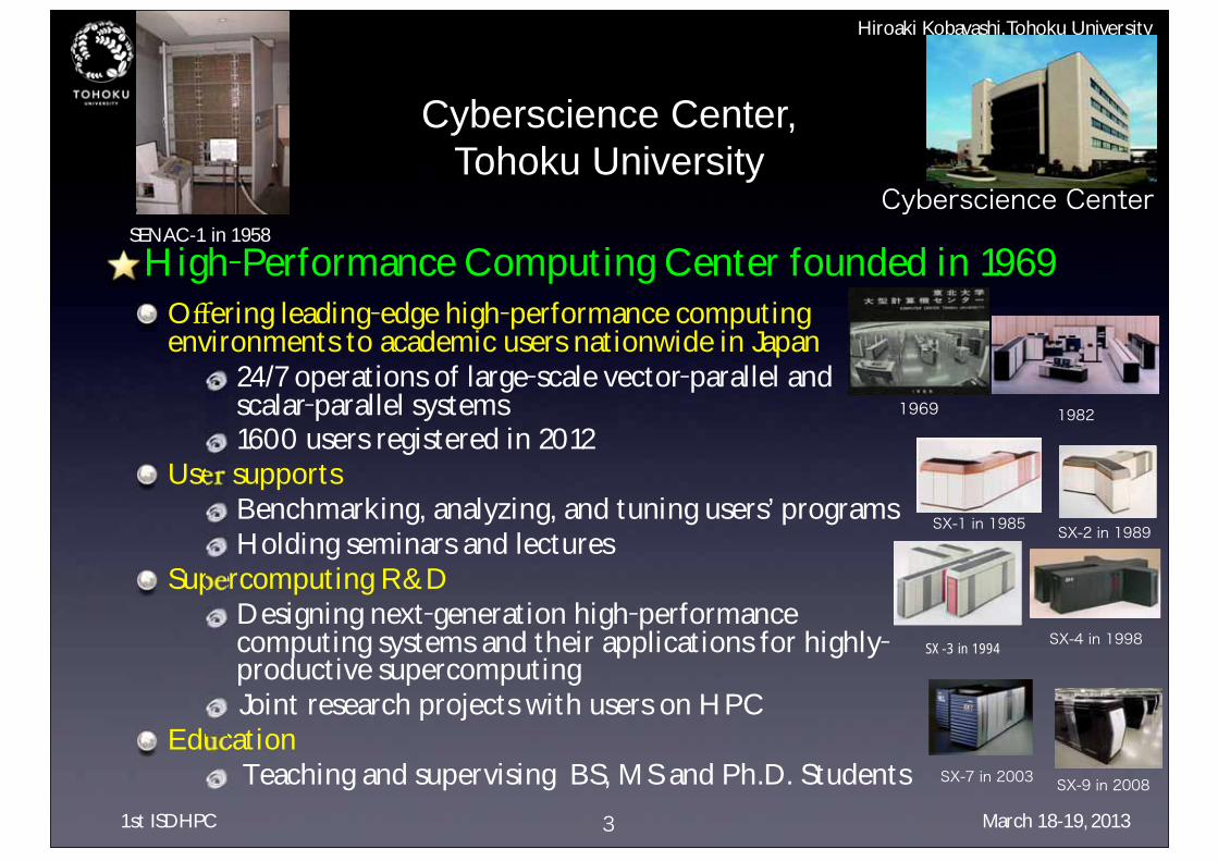
Cyberscience Center,Tohoku University
Offering leading-edge high-performance computing environments to academic users nationwide in Japan
24/7 operations of large-scale vector-parallel and scalar-parallel systems1600 users registered in 2012
User supportsBenchmarking, analyzing, and tuning users’ programsHolding seminars and lectures
Supercomputing R&DDesigning next-generation high-performance computing systems and their applications for highly-productive supercomputingJoint research projects with users on HPC
Education Teaching and supervising BS, MS and Ph.D. Students
3
Cyberscience Center
High-Performance Computing Center founded in 1969
1969 1982
SX-1 in 1985 SX-2 in 1989
SX-4 in 1998
SX-7 in 2003 SX-9 in 2008
SX-3 in 1994
SENAC-1 in 1958

Hiroaki Kobayashi, Tohoku University
1st ISDHPC March 18-19, 2013
Supercomputing Systems of Tohoku University
4
Installed in 2008Installed in 2010
Hiroaki Kobayashi, Tohoku University
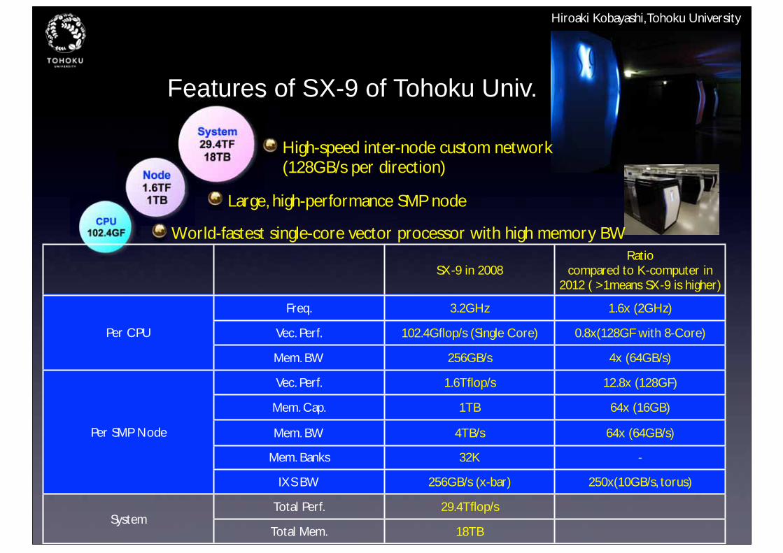
System29.4TF18TB High-speed inter-node custom network
(128GB/s per direction)Node1.6TF1TB Large, high-performance SMP node
Features of SX-9 of Tohoku Univ.
CPU102.4GF World-fastest single-core vector processor with high memory BW
SX-9 in 2008Ratio
compared to K-computer in 2012 ( >1means SX-9 is higher)
Freq. 3.2GHz 1.6x (2GHz)
Per CPU Vec. Perf. 102.4Gflop/s (Single Core) 0.8x(128GF with 8-Core)
Mem. BW 256GB/s 4x (64GB/s)
Vec. Perf. 1.6Tflop/s 12.8x (128GF)
Mem. Cap. 1TB 64x (16GB)
Per SMP Node Mem. BW 4TB/s 64x (64GB/s)
Mem. Banks 32K -
IXS BW 256GB/s (x-bar) 250x(10GB/s, torus)
SystemTotal Perf. 29.4Tflop/s
SystemTotal Mem. 18TB
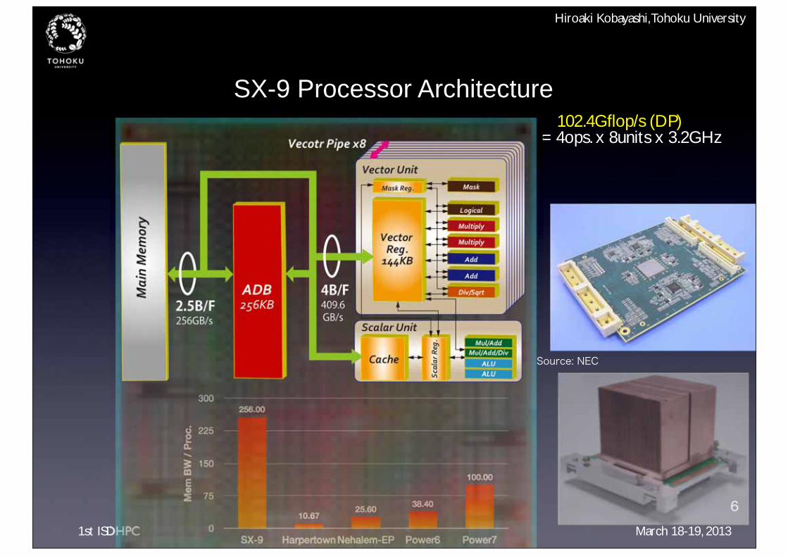
Hiroaki Kobayashi, Tohoku University
1st ISDHPC March 18-19, 2013
SX-9 Processor Architecture102.4Gflop/s (DP)
= 4ops. x 8units x 3.2GHz
60
75
150
225
300
SX-9 Harpertown Nehalem-EP Power6 Power7
Mem
BW
/ P
roc.
Source: NEC
Hiroaki Kobayashi, Tohoku University
1st ISDHPC March 18-19, 2013
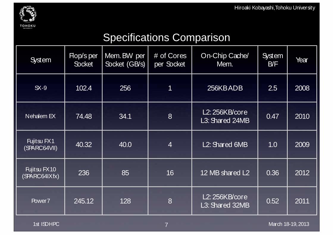
Specifications Comparison
7
SystemFlop/s per
SocketMem. BW per Socket (GB/s)
# of Cores per Socket
On-Chip Cache/Mem.
System B/F
Year
SX-9 102.4 256 1 256KB ADB 2.5 2008
Nehalem EX 74.48 34.1 8L2: 256KB/coreL3: Shared 24MB
0.47 2010
Fujitsu FX1(SPARC64VII) 40.32 40.0 4 L2: Shared 6MB 1.0 2009
Fujitsu FX10 (SPARC64IXfx) 236 85 16 12 MB shared L2 0.36 2012
Power7 245.12 128 8L2: 256KB/coreL3: Shared 32MB
0.52 2011
Hiroaki Kobayashi, Tohoku University
1st ISDHPC March 18-19, 2013
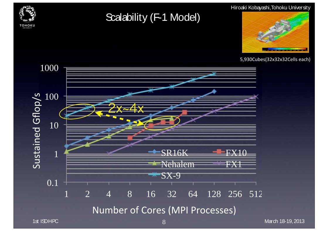
Scalability (F-1 Model)
8
0.1
1
10
100
1000
1 2 4 8 16 32 64 128 256 512
SR16K FX10 Nehalem FX1 SX-9
2x~4x
Hiroaki Kobayashi, Tohoku University
1st ISDHPC March 18-19, 2013
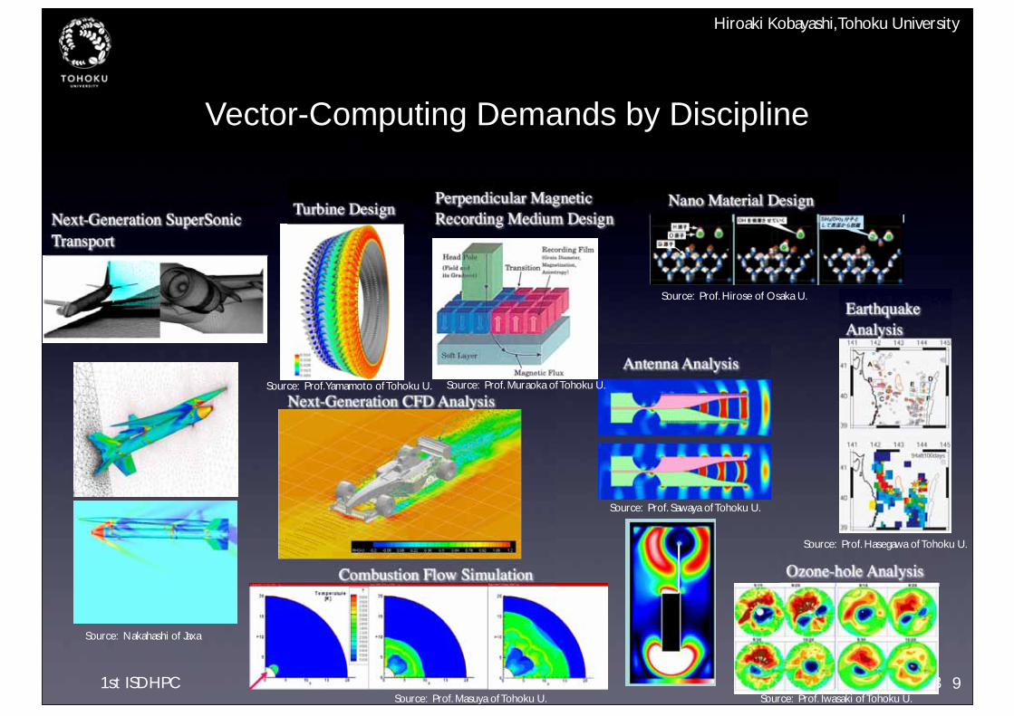
Vector-Computing Demands by Discipline
9
Source: Prof. Yamamoto of Tohoku U. Source: Prof. Muraoka of Tohoku U.
Source: Nakahashi of Jaxa
Source: Prof. Hirose of Osaka U.
Source: Prof. Sawaya of Tohoku U.
Source: Prof. Hasegawa of Tohoku U.
Source: Prof. Iwasaki of Tohoku U.Source: Prof. Masuya of Tohoku U.
Feasibility Study of A Future HPC System for Memory-Intensive Applications toward Post-Petascale/Exascale Computing
Hiroaki Kobayashi, Tohoku University
1st ISDHPC March 18-19, 2013
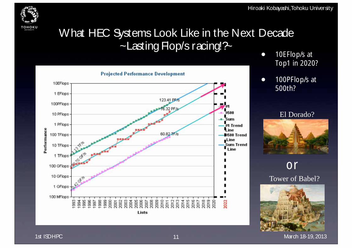
What HEC Systems Look Like in the Next Decade~Lasting Flop/s racing!?~
• 10EFlop/s at Top1 in 2020?
• 100PFlop/s at 500th?
11
2022
El Dorado?
Tower of Babel?
or
Hiroaki Kobayashi, Tohoku University
1st ISDHPC March 18-19, 2013
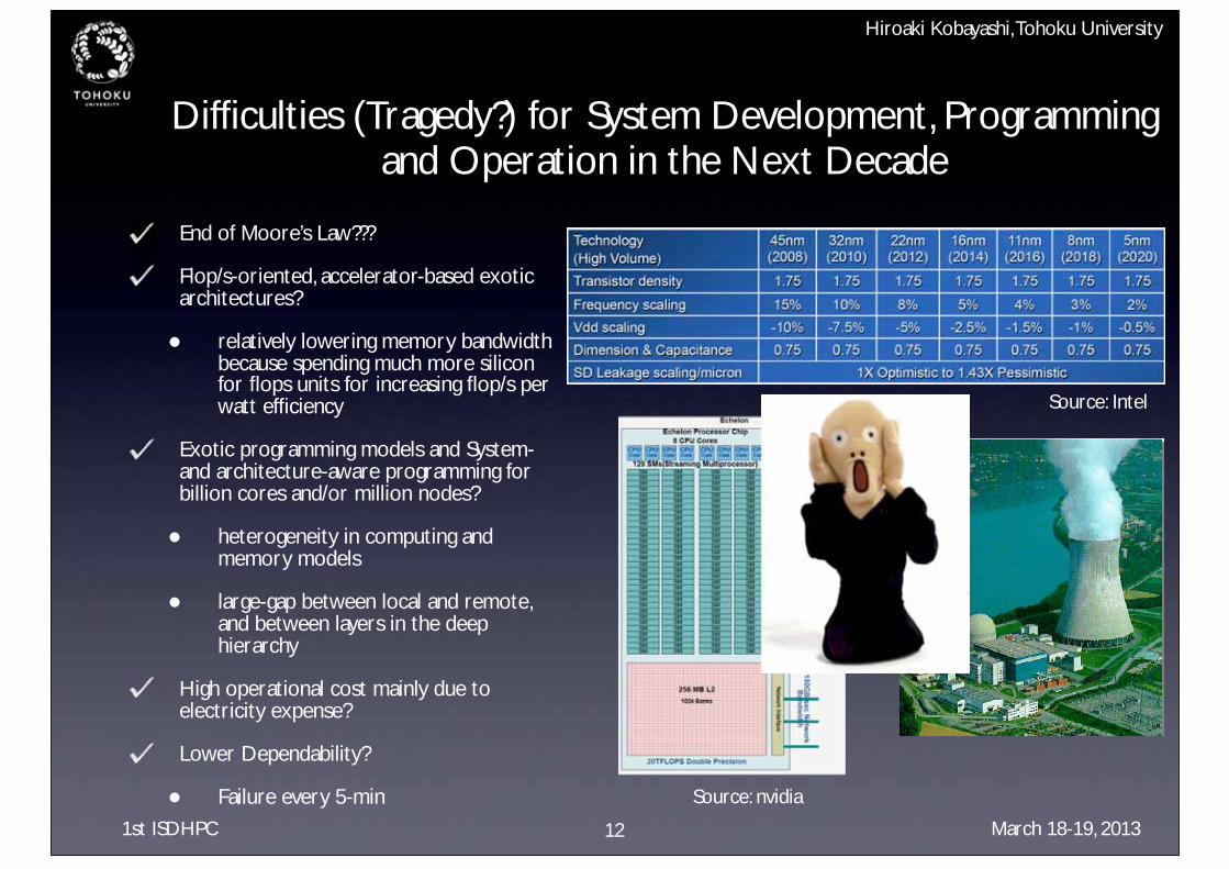
Difficulties (Tragedy?) for System Development, Programming and Operation in the Next Decade
End of Moore’s Law???
Flop/s-oriented, accelerator-based exotic architectures?
• relatively lowering memory bandwidth because spending much more silicon for flops units for increasing flop/s per watt efficiency
Exotic programming models and System- and architecture-aware programming for billion cores and/or million nodes?
• heterogeneity in computing and memory models
• large-gap between local and remote, and between layers in the deep hierarchy
High operational cost mainly due to electricity expense?
Lower Dependability?
• Failure every 5-min
12
Source: Intel
Source: nvidia

Hiroaki Kobayashi, Tohoku University
1st ISDHPC March 18-19, 2013
Applications May Change Players in HPC?~Memory Bandwidth-Oriented Systems vs. Flop/s Oriented Systems~
13
256.0
128.0
64.0
32.0
16.0
8.0
4.0
2.0
1.0
0.5
Att
aina
ble
Perf
orm
ance
(G
flops
/s)
Application B/F (Memory Access Intensity)
8 4 2 1 0.5 0.25 0.125 0.063
Stream
BW 72
.95GB/s
Tesla C1060 1.3B/F (78Gflop/s)
SX-9 2.5B/F(102.4Gflop/s)
Stream
BW 25
6GB/s
NGV 1B/F (256Gflop/s)
Stream
BW 17
.6GB/s
Nehalem EX 0.47B/F (72.48Gflop/s)
Stream
BW 17
.0GB/s
Nehalem EP 0.55B/F (46.93Gflop/s)
Stream
BW 34
.8GB/s
Sandy Bridge 0.27B/F (187.5Gflop/s)
Stream
BW 58
.61GB/s
Power7 0.52B/F(245.1Gflop/s)
Stream
BW 10
.0 GB/s
Stream
BW 43
.3GB/s
FX-1 1.0B/F (40.32Gflop/s)
FX-10 0.36B/F (236.5Gflop/s)
Stream
BW 64
.7GB/s
K computer 0.5B/F(128Gflop/s)
0.03 0.01
SX-8 4B/F (35.2Gflop/s)
For Memory intensive
applicationsFor Computation-
intensive applications
Source: 2012 report of computational science roadmap
Hiroaki Kobayashi, Tohoku University
1st ISDHPC March 18-19, 2013
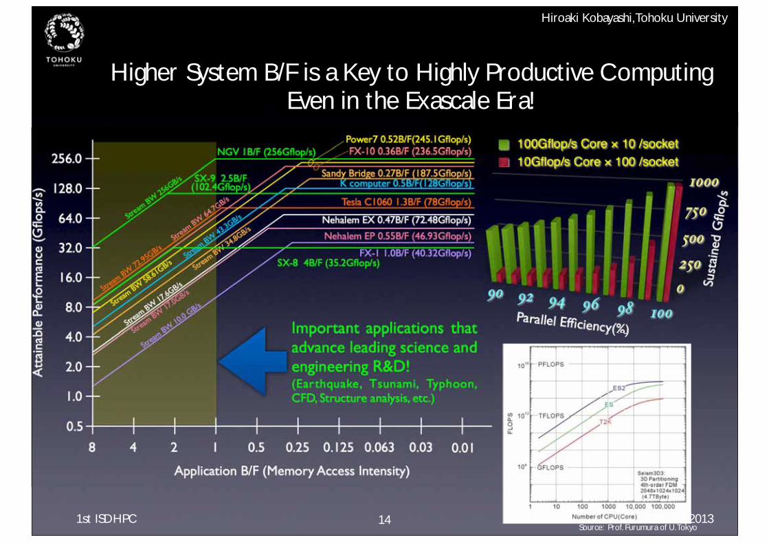
Higher System B/F is a Key to Highly Productive Computing Even in the Exascale Era!
14
Important applications that advance leading science and engineering R&D! (Earthquake, Tsunami, Typhoon, CFD, Structure analysis, etc.)
Parallel Efficiency(%)
Sust
aine
d G
flop/
s
256.0
128.0
64.0
32.0
16.0
8.0
4.0
2.0
1.0
0.5
Att
aina
ble
Perf
orm
ance
(G
flops
/s)
Application B/F (Memory Access Intensity)
8 4 2 1 0.5 0.25 0.125 0.063
Stream
BW 72
.95GB/s
Tesla C1060 1.3B/F (78Gflop/s)
SX-9 2.5B/F(102.4Gflop/s)
Stream
BW 25
6GB/s
NGV 1B/F (256Gflop/s)
Stream
BW 17
.6GB/s
Nehalem EX 0.47B/F (72.48Gflop/s)
Stream
BW 17
.0GB/s
Nehalem EP 0.55B/F (46.93Gflop/s)
Stream
BW 34
.8GB/s
Sandy Bridge 0.27B/F (187.5Gflop/s)
Stream
BW 58
.61GB/s
Power7 0.52B/F(245.1Gflop/s)
Stream
BW 10
.0 GB/s
Stream
BW 43
.3GB/s
FX-1 1.0B/F (40.32Gflop/s)
FX-10 0.36B/F (236.5Gflop/s)
Stream
BW 64
.7GB/s
K computer 0.5B/F(128Gflop/s)
0.03 0.01
SX-8 4B/F (35.2Gflop/s)
Source: Prof. Furumura of U. Tokyo
Hiroaki Kobayashi, Tohoku University
1st ISDHPC March 18-19, 2013
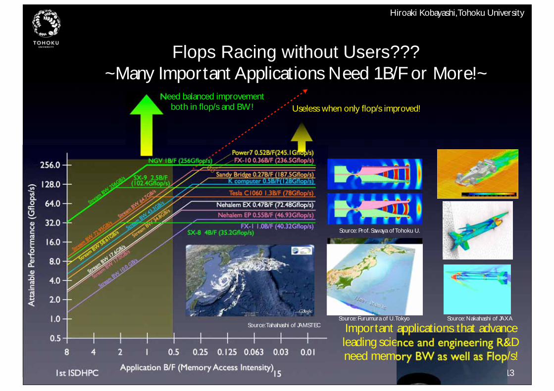
Flops Racing without Users??? ~Many Important Applications Need 1B/F or More!~
15
Important applications that advance leading science and engineering R&D need memory BW as well as Flop/s!
Need balanced improvement both in flop/s and BW! Useless when only flop/s improved!
256.0
128.0
64.0
32.0
16.0
8.0
4.0
2.0
1.0
0.5
Att
aina
ble
Perf
orm
ance
(G
flops
/s)
Application B/F (Memory Access Intensity)
8 4 2 1 0.5 0.25 0.125 0.063
Stream
BW 72
.95GB/s
Tesla C1060 1.3B/F (78Gflop/s)
SX-9 2.5B/F(102.4Gflop/s)
Stream
BW 25
6GB/s
NGV 1B/F (256Gflop/s)
Stream
BW 17
.6GB/s
Nehalem EX 0.47B/F (72.48Gflop/s)
Stream
BW 17
.0GB/s
Nehalem EP 0.55B/F (46.93Gflop/s)
Stream
BW 34
.8GB/s
Sandy Bridge 0.27B/F (187.5Gflop/s)
Stream
BW 58
.61GB/s
Power7 0.52B/F(245.1Gflop/s)
Stream
BW 10
.0 GB/s
Stream
BW 43
.3GB/s
FX-1 1.0B/F (40.32Gflop/s)
FX-10 0.36B/F (236.5Gflop/s)
Stream
BW 64
.7GB/s
K computer 0.5B/F(128Gflop/s)
0.03 0.01
SX-8 4B/F (35.2Gflop/s)
Source: Tahahashi of JAMSTECSource: Furumura of U. Tokyo
Source: Prof. Sawaya of Tohoku U.
Source: Nakahashi of JAXA
Hiroaki Kobayashi, Tohoku University
1st ISDHPC March 18-19, 2013
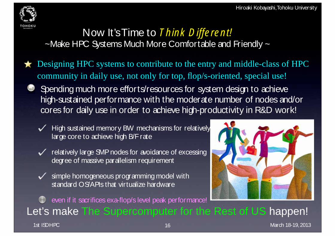
Now It’s Time to Think Different!~Make HPC Systems Much More Comfortable and Friendly ~
High sustained memory BW mechanisms for relatively large core to achieve high B/F rate
relatively large SMP nodes for avoidance of excessing degree of massive parallelism requirement
simple homogeneous programming model with standard OS/APIs that virtualize hardware
even if it sacrifices exa-flop/s level peak performance!
16
Let’s make The Supercomputer for the Rest of US happen!
Designing HPC systems to contribute to the entry and middle-class of HPC community in daily use, not only for top, flop/s-oriented, special use!
Spending much more efforts/resources for system design to achieve high-sustained performance with the moderate number of nodes and/or cores for daily use in order to achieve high-productivity in R&D work!

Hiroaki Kobayashi, Tohoku University
1st ISDHPC March 18-19, 2013
Feasibility Study of Future HPC Systems for Memory Intensive-Applications
Tohoku Univ., NEC and JAMSTEC team that investigate the feasibility of a mult-vectorcore architecture with a high-memory bandwidth for memory intensive applications
Target areas: memory-intensive applications that need high B/F rates
• Analysis of Planet Earth Variations for Mitigating Natural Disasters
weather, climate, environment changes, earthquake, tsunami
• Advanced simulation tools that accelerate industrial innovation
CFD, Structural analysis, material design ...
17
Source: Kaneda of JAMSTEC Source: Tahahashi of JAMSTECSource: Furumura of U. TokyoSource: Nakahashi of JAXA
Source: Prof. Yamamoto of Tohoku U.Source: Prof. Imamura&Koshimura of Tohoku U.Source: Prof. Hori of U. Tokyo

Hiroaki Kobayashi, Tohoku University
1st ISDHPC March 18-19, 2013
Team Organization
18
Application ResearchGroup
System ResearchGroup
Device TechnologiesResearch Group
Tohoku University Leader Hiroaki Kobayashi)
Jamstec (Co-Leaders: Yoshiyuki Kaneda & Kunihiko Watanabe)
(Takahashi, Hori, Itakura, Uehara, et al.)
NEC (Leader: Yukiko Hashimoto)(Hagiwara, Momose, Musa, Watanabe, Hayashi, Nakazato, et al.)
Imamura, Koshimura, Yamamoto, Matsuoka,
Toyokuni et al.Applications
Egawa, Architecture
Takizawa, Sys. Soft.
Muraoka, Storage
Koyanagi, et al. 3D Device
Hanyu, NV Mem.
Furumura, Hori et al. University of Tokyo
Applications
Nakahashi, JAXAApplications
Hasegawa, Arakawa, Osaka University, Network
Sato, JAIST, Sys. Soft.
Yokokawa, Uno, RikenSys. Soft & I/O & Storage
Motoyoshi, Tohoku MicroTec3D Device Fab.
Sano, Network
Komatsu, Benchmark

Hiroaki Kobayashi, Tohoku University
1st ISDHPC March 18-19, 2013
Exascale Computing Requirements in 2020
19
Hiroaki Kobayashi, Tohoku University
1st ISDHPC March 18-19, 2013
Other Demands for Future HPC systems
High processing efficiency
memory subsystem that realizes 2B/F or More (hopefully 4B/F)!
Efficient handling of short vectors and indirect memory access
• gather/scatter
High sustained performance and scalability with moderate degree of parallelism
Keep the number of cores/socket and nodes as small as possible to obtain the target performance
• larger processing granularity of core performance for MPI processing
Low MPI communication overhead
System software to provides standard programming environment and flexible, power-efficient, and fault-tolerant operation capability, while keeping high sustained performance of individual applications
20

Hiroaki Kobayashi, Tohoku University
1st ISDHPC March 18-19, 2013
N
21
StandardizationCustomization
Shorten time to solution/market
Reduce development cost
Increase operation efficiency
Desire to differentiate from others
More performance
Less Power/Energy
Standard design methodology
and tools
Open source software
&Standard library/user
interface
Innov
ative
devic
es
New ar
chite
cture
s
Friendly Programming Models and API
High B/F. Big Core and Large SMP
N
So What to Do~Our Approach based on Design Pendulum~
Hiroaki Kobayashi, Tohoku University
Hiroaki Kobayashi, Tohoku University
1st ISDHPC March 18-19, 2013
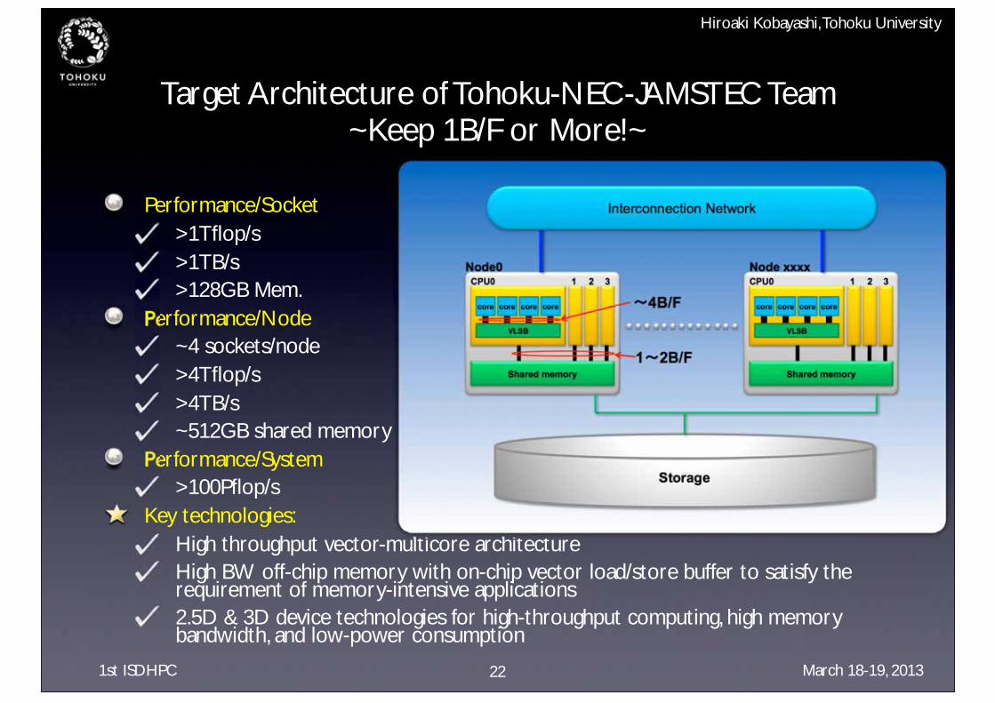
Target Architecture of Tohoku-NEC-JAMSTEC Team~Keep 1B/F or More!~
Performance/Socket>1Tflop/s>1TB/s>128GB Mem.
Performance/Node~4 sockets/node>4Tflop/s>4TB/s~512GB shared memory
Performance/System>100Pflop/s
Key technologies:High throughput vector-multicore architectureHigh BW off-chip memory with on-chip vector load/store buffer to satisfy the requirement of memory-intensive applications2.5D & 3D device technologies for high-throughput computing, high memory bandwidth, and low-power consumption
22
VLSB
core core core core
Shared memory
CPU0 1 2 3Node0
VLSB
core core core core
Shared memory
CPU0 1 2 3Node xxxx
Storage
Interconnection Network
1 2B/F
4B/F
1st ISDHPC March 18-19, 2013
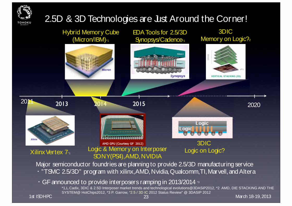
2.5D & 3D Technologies are Just Around the Corner!Hybrid Memory Cube
(Micron/IBM)*1
2020201520142013
Xilinx Vertex 7*1
EDA Tools for 2.5/3DSynopsys/Cadence*1
Logic & Memory on InterposerSONY(PS4), AMD, NVIDIA
3DIC Logic on Logic?
3DICMemory on Logic?*2
*1,L.Cadix, 3DIC & 2.5D Interposer market trends and technological evolutions@3DASiP2012, *2 AMD, DIE STACKING AND THE SYSTEM@ HotChips2012, *3 P. Garrow, “2.5 / 3D IC 2012 Status Review” @ 3DASIP 2012
2011
Major semiconductor foundries are planning to provide 2.5/3D manufacturing service ・”TSMC 2.5/3D” program with xilinx, AMD, Nvidia, Qualcomm, TI, Marvell, and Altera
・GF announced to provide interposers ramping in 2013/2014 *3
23

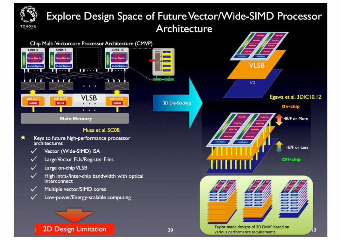
Design Space Exploration of the Vector Processor Architecture using 2.5/3D Die-Stacking Technology
1st ISDHPC March 18-19, 2013
0
15
30
45
60
25
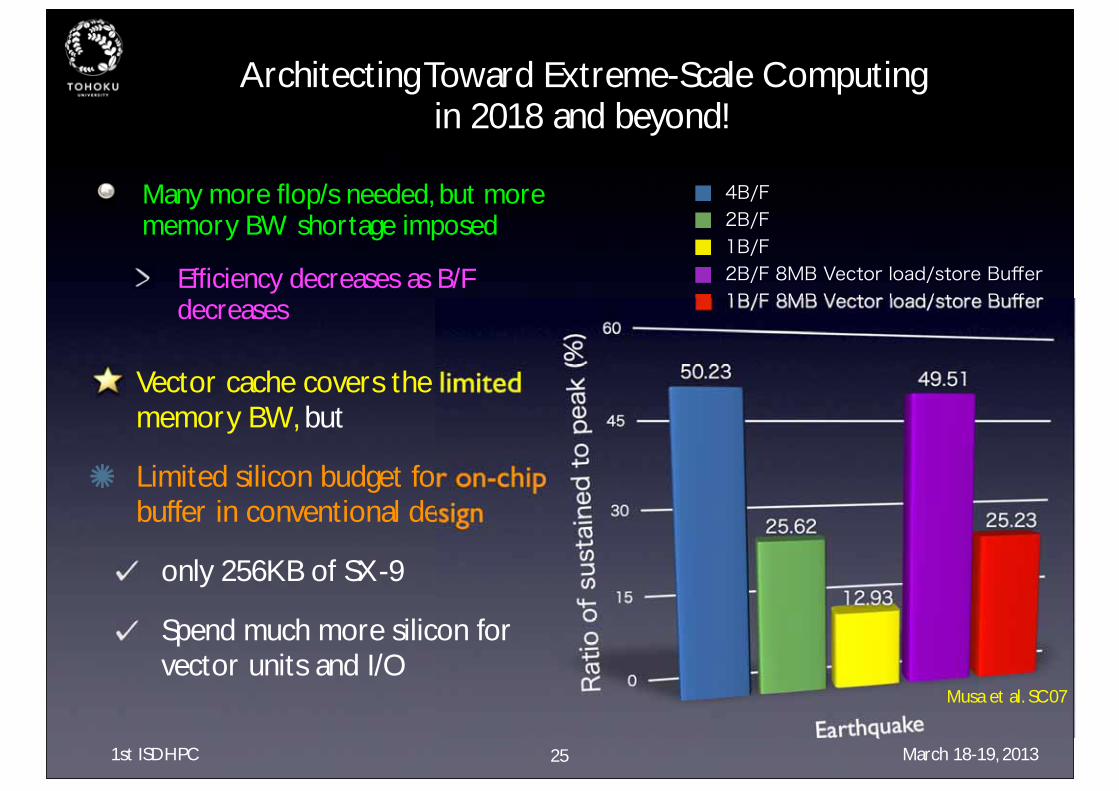
Architecting Toward Extreme-Scale Computing in 2018 and beyond!
4B/F2B/F 1B/F 2B/F 8MB Vector load/store Buffer1B/F 8MB Vector load/store Buffer
Earthquake
Ratio
of s
usta
ined
to p
eak
(%)
Many more flop/s needed, but more memory BW shortage imposed
Efficiency decreases as B/F decreases
Vector cache covers the limited memory BW, but
Limited silicon budget for on-chip buffer in conventional design
only 256KB of SX-9
Spend much more silicon for vector units and I/O
Musa et al. SC07
1st ISDHPC March 18-19, 201326
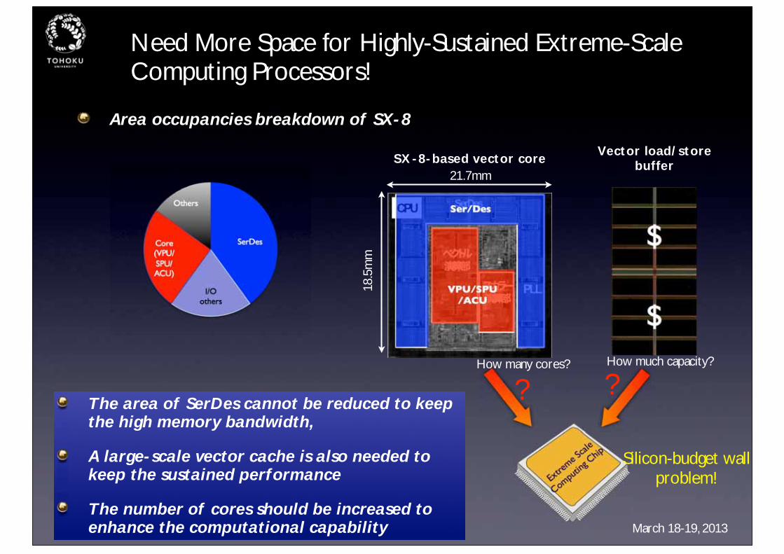
Need More Space for Highly-Sustained Extreme-Scale Computing Processors!
Area occupancies breakdown of SX-8
SerDes
I/O others
Core (VPU/SPU/ACU)
OthersSer/Des
VPU/SPU/ACU
21.7mm
18.5
mm
$
$
SX-8-based vector coreVector load/store
buffer
Extre
me Scal
e
Computin
g Chip
The area of SerDes cannot be reduced to keep the high memory bandwidth,
A large-scale vector cache is also needed to keep the sustained performance
The number of cores should be increased to enhance the computational capability
? ?How many cores? How much capacity?
Silicon-budget wall problem!
1st ISDHPC March 18-19, 201327
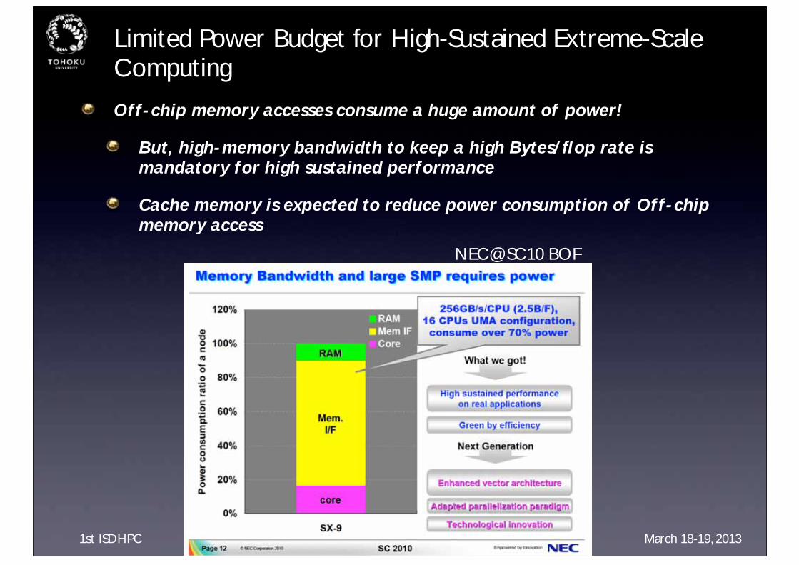
Limited Power Budget for High-Sustained Extreme-Scale Computing
Off-chip memory accesses consume a huge amount of power!
But, high-memory bandwidth to keep a high Bytes/flop rate is mandatory for high sustained performance
Cache memory is expected to reduce power consumption of Off-chip memory access
NEC@SC10 BOF
1st ISDHPC March 18-19, 2013
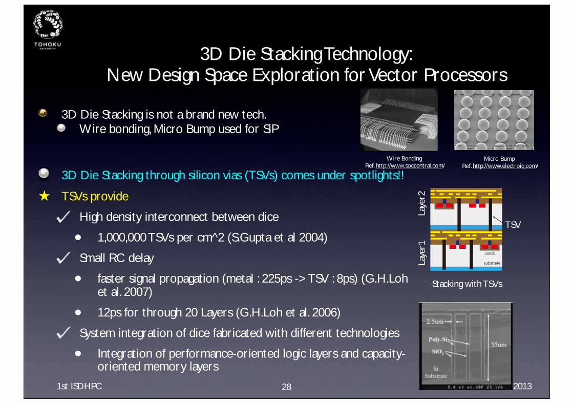
3D Die Stacking Technology:New Design Space Exploration for Vector Processors
3D Die Stacking is not a brand new tech.Wire bonding, Micro Bump used for SiP
3D Die Stacking through silicon vias (TSVs) comes under spotlights!!
TSVs provide
High density interconnect between dice
• 1,000,000 TSVs per cm^2 (S.Gupta et al 2004)
Small RC delay
• faster signal propagation (metal : 225ps -> TSV : 8ps) (G.H.Loh et al. 2007)
• 12ps for through 20 Layers (G.H.Loh et al. 2006)
System integration of dice fabricated with different technologies
• Integration of performance-oriented logic layers and capacity-oriented memory layers
28
Wire Bonding Ref. http://www.soccentral.com/
Micro Bump Ref. http://www.electroiq.com/
substrate
CMOS
TSV
Stacking with TSVs
Laye
r1La
yer2

1st ISDHPC March 18-19, 2013
Preliminary Evaluations of TSVClarifying the potential of TSVs in terms of power, delay, and cost
・Simulation : SPICE・Parameters (TSVs and CMOS tech) : Based on ITRS・Transistor size : Minimizing DelayMicroBump T: 95mΩ,5.4fF
=
TSV2D Wire
?? µmm
30 Egawa et al. 3DIC12

1st ISDHPC March 18-19, 2013
Potential of TSVs (Delay)
TSV diameter (Length = 50µmm fixed)
Equi
vale
nt 2
D W
ire
Leng
th (
µmm
)
31
Egawa et al. 3DIC12
1st ISDHPC March 18-19, 2013
3D
Vector Processor
Onchip memoryVector Processor
Onchip memory
x[0 : 31] y[0 : 31]
x[0 : 15]x[16 : 31]
y[0 : 15]y[16 : 31]
3D
3D
REG
ALU
REG
ALUTSV
3D
Vector Processor
Vector ProcessorVector Processor Vector Processor
ALU bit splitting
ALU on Register
Onchip memory on Core
Core on Core
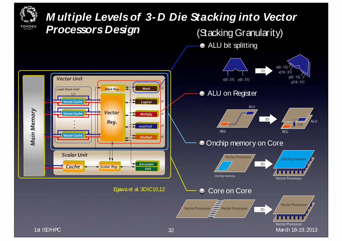
Multiple Levels of 3-D Die Stacking into Vector Processors Design (Stacking Granularity)
32
Egawa et al. 3DIC10,12
1st ISDHPC March 18-19, 2013
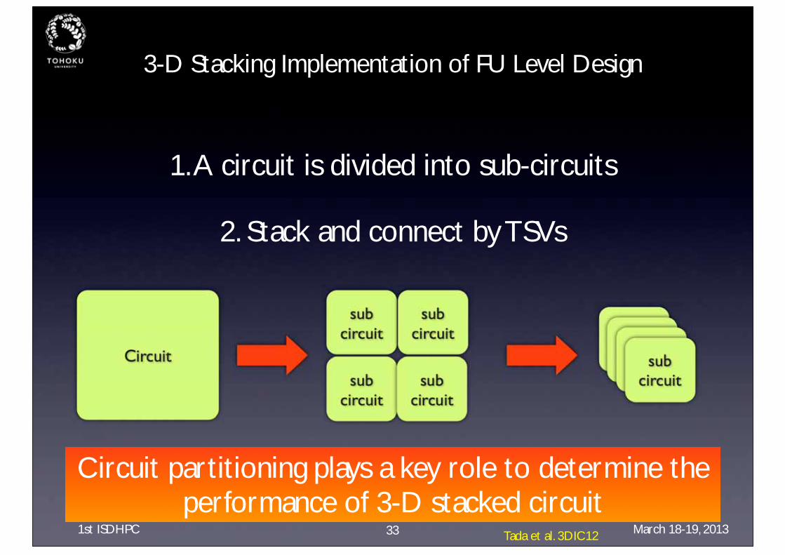
3-D Stacking Implementation of FU Level Design
1. A circuit is divided into sub-circuits
2. Stack and connect by TSVs
Circuit partitioning plays a key role to determine the performance of 3-D stacked circuit
33 Tada et al. 3DIC12
1st ISDHPC March 18-19, 2013
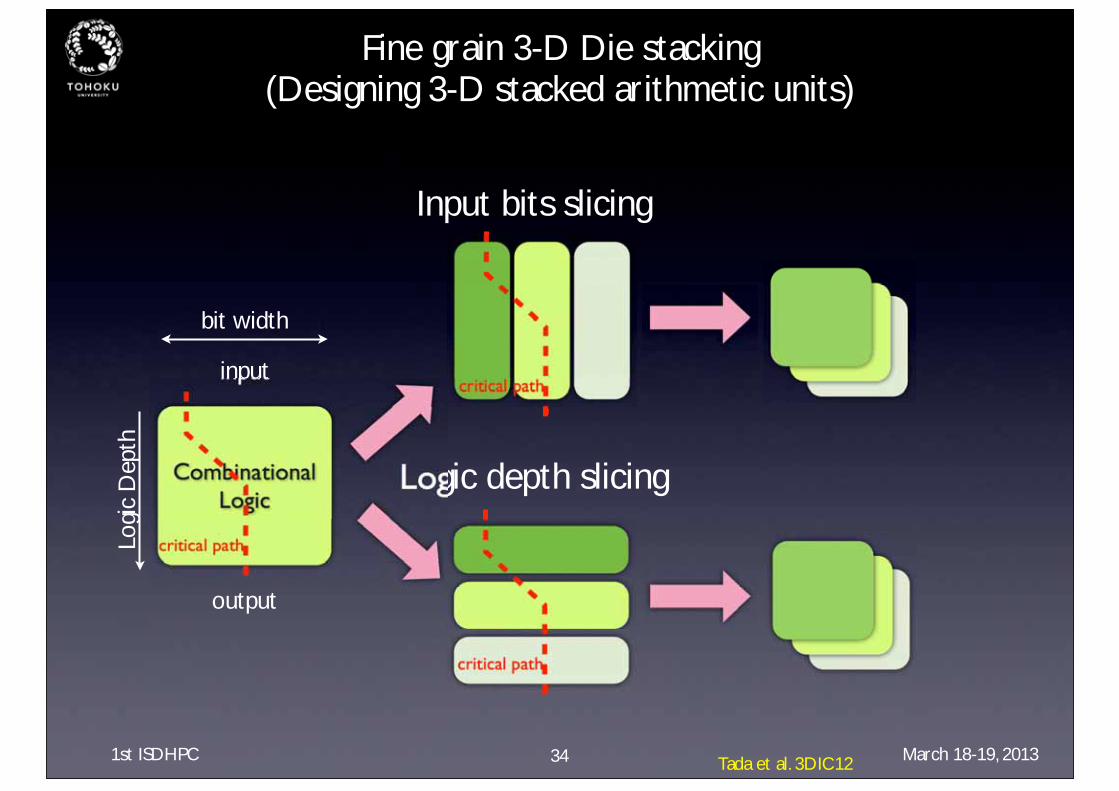
Fine grain 3-D Die stacking (Designing 3-D stacked arithmetic units)
input
output
Logi
c D
epth
critical path
critical path
critical path
Input bits slicing
Logic depth slicing
bit width
34 Tada et al. 3DIC12
1st ISDHPC March 18-19, 2013
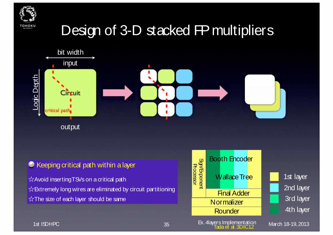
Design of 3-D stacked FP multipliers
input
output
Logi
c D
epth
critical path
Keeping critical path within a layer
☆Avoid inserting TSVs on a critical path
☆Extremely long wires are eliminated by circuit partitioning
☆The size of each layer should be same
Wallace Tree
Booth Encoder
Final AdderNormalizer
Rounder
Sign/Exponent Processor
Ex. 4layers Implementation
1st layer
2nd layer
3rd layer
4th layer
bit width
35 Tada et al. 3DIC12

1st ISDHPC March 18-19, 2013
Effects of a 3D Die-Stacking FP Multiplier Design
0
3
6
9
12
15
8layers4layers2layers2D8layers4layers2layers2D
Del
ay (
ns)
Single precision FP Double precision FP
Appropriate circuit partitioning can exploit the potential of 3D stacking technologies in arithmetic unit designs
9% 16% 42%
Delay reduction
1% 8% 28%Delay reduction
36 Tada et al. 3DIC12

1st ISDHPC March 18-19, 2013
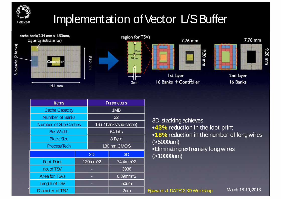
Design Strategies of 3D Stacked Vector L/S Buffer
TSVs region
Sub Cache(bank)Controller
Data array Tag array
the longest wire
Course grain partitioning supports replacing long wires between controller and banks by TSV
-- Eliminating the long wires contributes to both power and delay reduction
TSVs regions are placed to the out side of coresBanks are paced near the TSVs region
The longest wire connects
banks and controller
37
Chip Photo
14.1 mm
9.20 mm
2D Design 3D Design (2-layer)
Egawa et al. DATE12 3D Workshop
1st ISDHPC March 18-19, 2013
Implementation of Vector L/S Buffer
items Parameters
Cache Capacity 1MB
Number of Banks 32
Number of Sub-Caches 16 (2 banks/sub-cache)
Bus Width 64 bits
Block Size 8 Byte
Process Tech 180 nm CMOS
2D 3D
Foot Print 130mm^2 74.4mm^2
no. of TSV - 3936
Area for TSVs - 0.39mm^2
Length of TSV - 50um
Diameter of TSV 2um
cache bank(2.34 mm x 1.53mm, tag array &data array)
14.1 mm
9.20 mm
Controller
Sub-
cach
e (2
ban
ks)
10um
10um
1st layer 2nd layer
region for TSVs7.76 mm
9.20 mm
7.76 mm
9.20 mm
16 Banks +Controller 16 Banks 2um 12
3D stacking achieves•43% reduction in the foot print•18% reduction in the number of long wires (>5000um)•Eliminating extremely long wires(>10000um)
Egawa et al. DATE12 3D Workshop
1st ISDHPC March 18-19, 201339
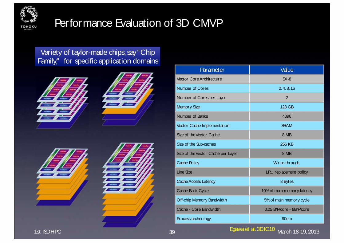
Performance Evaluation of 3D CMVP
Parameter Value
Vector Core Architecture SX-8
Number of Cores 2, 4, 8, 16
Number of Cores per Layer 2
Memory Size 128 GB
Number of Banks 4096
Vector Cache Implementation SRAM
Size of the Vector Cache 8 MB
Size of the Sub-caches 256 KB
Size of the Vector Cache per Layer 8 MB
Cache Policy Write-through,
Line Size LRU replacement policy
Cache Access Latency 8 Bytes
Cache Bank Cycle 10% of main memory latency
Off-chip Memory Bandwidth 5% of main memory cycle
Cache - Core Bandwidth 0.25 B/F/core - 8B/F/core
Process technology 90nm
Variety of taylor-made chips, say “Chip Family,” for specific application domains
Egawa et al. 3DIC10

1st ISDHPC March 18-19, 2013
Impacts of 3D Die-Stacking on 3D-CMVP Design
Effects of Enhancing Memory BW
☆Enhancing off-chip memory BW improves the sustained performance with high-scalability
☆Introducing Vector Load/Store Buffer also improves the performance
Rel
ativ
e Pe
rfor
man
ce
the performance is normalized by the single core, without VLSB, with baseline off-chip memory BW case
0
3
6
9
12
2 cores 4 cores 8 cores 16cores
0.25B/F
0.5B/F
1B/F
2B/F
0.5B/F
1B/F
4B/F
2B/F
1B/F
8B/F
4B/F
2B/F
Effects of employing an 8MB VLSB
Rel
ativ
e Pe
rfor
man
ce0
3
6
9
12
2 cores 4 cores 8 cores 16cores
0.25B/F
0.5B/F
1B/F
2B/F
0.5B/F
1B/F
4B/F
2B/F
1B/F
4B/F
2B/F
highlow
highlow
Off chip mem BW
1x 2x 4x
40
FDTD Code
Egawa et al. 3DIC10
1st ISDHPC March 18-19, 2013
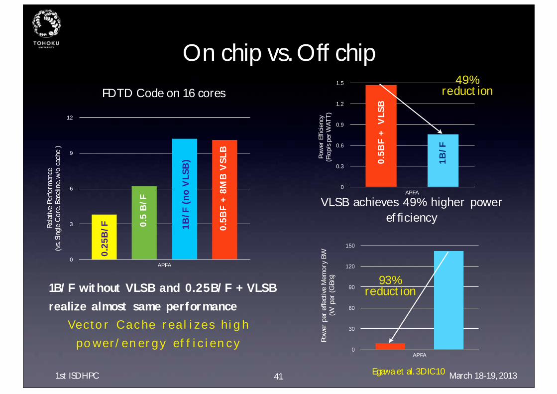
On chip vs. Off chip
0
3
6
9
12
APFA
0.2
5B
/F 0.5
B/F
1B
/F (
no
VLS
B)
0.5
BF
+ 8
MB
VS
LB
Rel
ativ
e Pe
rfor
man
ce
(vs.
Sing
le C
ore.
Bas
elin
e. w
/o c
ache
)
0
0.3
0.6
0.9
1.2
1.5
APFA
Pow
er E
ffici
ency
(Flo
p/s
per W
ATT
)
1B
/F
VLSB achieves 49% higher power efficiency
FDTD Code on 16 cores
1B/F without VLSB and 0.25B/F + VLSB realize almost same performance
0
30
60
90
120
150
APFA
Pow
er p
er e
ffect
ive
Mem
ory
BW(W
per
(G
B/s)
Vector Cache realizes high power/energy efficiency
93%reduction
0.5
BF
+
VLS
B41
49%reduction
Egawa et al. 3DIC10
1st ISDHPC March 18-19, 2013
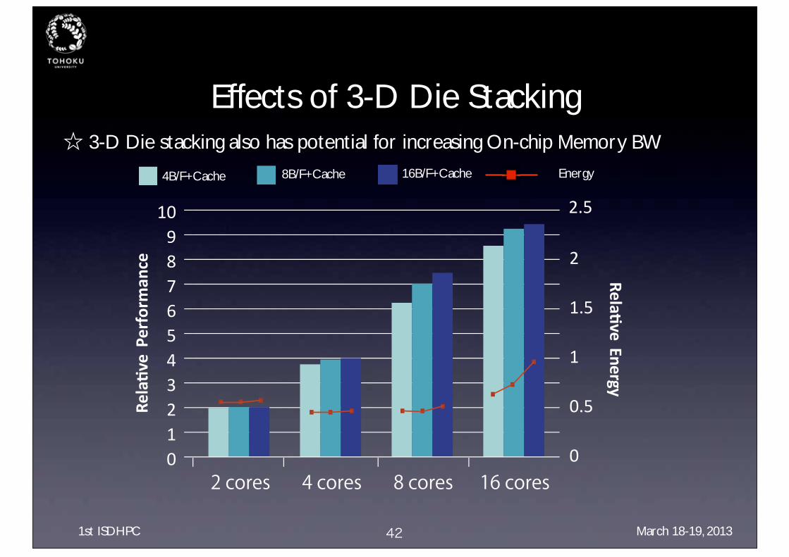
Effects of 3-D Die Stacking☆ 3-D Die stacking also has potential for increasing On-chip Memory BW
4B/F+Cache 8B/F+Cache 16B/F+Cache
2 cores 4 cores 8 cores 16 cores
Energy
42
1st ISDHPC March 18-19, 2013
Summary
Well balanced HEC systems regarding memory performance is still key to high productivity in science and engineering in the post peta-scale era
Great potential of the new generation vector architecture with 2.5D/3D die-stacking technologies
Extending the design space of the vector architecture by Increasing the number of cores, Enhancing I/O performance and Introducing vector cache mechanism contribute to realize high-performance computing.
High sustained memory BW to fuel vector function units with lower power/energy expected.
The vector cache can boost the sustained memory bandwidth energy-efficiently
When such new technologies will be available as production services?
Design tools, fab. and markets steer the future of the technologies! 43