
FCC Test Report (PART 22) · FCC Test Report (PART 22) Report No.: RF170810C05A FCC ID: 2ANKMFS040U...
52
Report No.: RF170810C05A Page No. 1 / 52 Report Format Version: 6.1.1 Reference No.: 170811C04 FCC Test Report (PART 22) Report No.: RF170810C05A FCC ID: 2ANKMFS040U Test Model: FS040U Received Date: Aug. 11, 2017 Test Date: Aug. 16, 2017 ~ Aug. 20, 2017 Issued Date: Aug. 31, 2017 Applicant: Shanghai Tricheer Technology Co., Ltd. Address: Rm 907, Building 1, Lane 399, Shengxia Road, Zhangjiang Hi-Tech Park, Pudong District, Shanghai Issued By: Bureau Veritas Consumer Products Services (H.K.) Ltd., Taoyuan Branch Lab Address: No. 47-2, 14th Ling, Chia Pau Vil., Lin Kou Dist., New Taipei City, Taiwan ( R.O.C ) Test Location (1): No. 19, Hwa Ya 2nd Rd, Wen Hwa Tsuen, Kwei Shan Hsiang, Taoyuan Hsien 333, Taiwan, R.O.C. Test Location (2): No.215, Sec. 3, Beixin Rd., Xindian Dist., New Taipei City 231, Taiwan, R.O.C This report is for your exclusive use. Any copying or replication of this report to or for any other person or entity, or use of our name or trademark, is permitted only with our prior written permission. This report sets forth our findings solely with respect to the test samples identified herein. The results set forth in this report are not indicative or representative of the quality or characteristics of the lot from which a test sample was taken or any similar or identical product unless specifically and expressly noted. Our report includes all of the tests requested by you and the results thereof based upon the information that you provided to us. You have 60 days from date of issuance of this report to notify us of any material error or omission caused by our negligence, provided, however, that such notice shall be in writing and shall specifically address the issue you wish to raise. A failure to raise such issue within the prescribed time shall constitute your unqualified acceptance of the completeness of this report, the tests conducted and the correctness of the report contents. Unless specific mention, the uncertainty of measurement has been explicitly taken into account to declare the compliance or non-compliance to the specification. The report must not be used by the client to claim product certification, approval, or endorsement by TAF or any government agencies
Transcript of FCC Test Report (PART 22) · FCC Test Report (PART 22) Report No.: RF170810C05A FCC ID: 2ANKMFS040U...
Report No.: RF170810C05A Page No. 1 / 52 Report Format Version: 6.1.1 Reference No.: 170811C04
FCC Test Report
(PART 22)
Report No.: RF170810C05A
FCC ID: 2ANKMFS040U
Test Model: FS040U
Received Date: Aug. 11, 2017
Test Date: Aug. 16, 2017 ~ Aug. 20, 2017
Issued Date: Aug. 31, 2017
Applicant: Shanghai Tricheer Technology Co., Ltd.
Address: Rm 907, Building 1, Lane 399, Shengxia Road, Zhangjiang Hi-Tech Park, Pudong District, Shanghai
Issued By: Bureau Veritas Consumer Products Services (H.K.) Ltd., Taoyuan Branch
Lab Address: No. 47-2, 14th Ling, Chia Pau Vil., Lin Kou Dist., New Taipei City, Taiwan ( R.O.C )
Test Location (1): No. 19, Hwa Ya 2nd Rd, Wen Hwa Tsuen, Kwei Shan Hsiang, Taoyuan Hsien 333, Taiwan, R.O.C.
Test Location (2): No.215, Sec. 3, Beixin Rd., Xindian Dist., New Taipei City 231, Taiwan, R.O.C
This report is for your exclusive use. Any copying or replication of this report to or for any other person or entity, or use of our name or trademark, is permitted only with our prior written permission. This report sets forth our findings solely with respect to the test samples identified herein. The results set forth in this report are not indicative or representative of the quality or characteristics of the lot from which a test sample was taken or any similar or identical product unless specifically and expressly noted. Our report includes all of the tests requested by you and the results thereof based upon the information that you provided to us. You have 60 days from date of issuance of this report to notify us of any material error or omission caused by our negligence, provided, however, that such notice shall be in writing and shall specifically address the issue you wish to raise. A failure to raise such issue within the prescribed time shall constitute your unqualified acceptance of the completeness of this report, the tests conducted and the correctness of the report contents. Unless specific mention, the uncertainty of measurement has been explicitly taken into account to declare the compliance or non-compliance to the specification. The report must not be used by the client to claim product certification, approval, or endorsement by TAF or any government agencies
Report No.: RF170810C05A Page No. 2 / 52 Report Format Version: 6.1.1 Reference No.: 170811C04
Table of Contents Release Control Record .................................................................................................................................. 3
1 Certificate of Conformity ........................................................................................................................... 4
2 Summary of Test Results ........................................................................................................................... 5
2.1 Measurement Uncertainty ..................................................................................................................... 5 2.2 Test Site and Instruments ..................................................................................................................... 6
3 General Information ................................................................................................................................... 7
3.1 General Description of EUT .................................................................................................................. 7 3.2 Configuration of System under Test ...................................................................................................... 8
3.2.1 Description of Support Units ....................................................................................................... 8 3.3 Test Mode Applicability and Tested Channel Detail .............................................................................. 9 3.4 EUT Operating Conditions .................................................................................................................. 10 3.5 General Description of Applied Standards .......................................................................................... 10
4 Test Types and Results ............................................................................................................................. 11
4.1 Output Power Measurement ................................................................................................................ 11 4.1.1 Limits of Output Power Measurement ....................................................................................... 11 4.1.2 Test Procedures ......................................................................................................................... 11 4.1.3 Test Setup ................................................................................................................................. 12 4.1.4 Test Results .............................................................................................................................. 13
4.2 Frequency Stability Measurement ...................................................................................................... 18 4.2.1 Limits of Frequency Stabiliity Measurement ............................................................................. 18 4.2.2 Test Procedure ......................................................................................................................... 18 4.2.3 Test Setup ................................................................................................................................. 18 4.2.4 Test Results .............................................................................................................................. 19
4.3 Occupied Bandwidth Measurement .................................................................................................... 24 4.3.1 Test Procedure ......................................................................................................................... 24 4.3.2 Test Setup ................................................................................................................................. 24 4.3.3 Test Result ................................................................................................................................ 25
4.4 Band Edge Measurement ................................................................................................................... 28 4.4.1 Limits of Band Edge Measurement .......................................................................................... 28 4.4.2 Test Setup ................................................................................................................................. 28 4.4.3 Test Procedures ........................................................................................................................ 28 4.4.4 Test Results .............................................................................................................................. 29
4.5 Peak to Average Ratio ........................................................................................................................ 34 4.5.1 Limits of Peak to Average Ratio Measurement ........................................................................ 34 4.5.2 Test Setup ................................................................................................................................. 34 4.5.3 Test Procedures ........................................................................................................................ 34 4.5.4 Test Results .............................................................................................................................. 35
4.6 Conducted Spurious Emissions .......................................................................................................... 38 4.6.1 Limits of Conducted Spurious Emissions Measurement .......................................................... 38 4.6.2 Test Setup ................................................................................................................................. 38 4.6.3 Test Procedure ......................................................................................................................... 38 4.6.4 Test Results .............................................................................................................................. 39
4.7 Radiated Emission Measurement ....................................................................................................... 44 4.7.1 Limits of Radiated Emission Measurement .............................................................................. 44 4.7.2 Test Procedure ......................................................................................................................... 44 4.7.3 Deviation from Test Standard ................................................................................................... 44 4.7.4 Test Setup ................................................................................................................................. 44 4.7.5 Test Results .............................................................................................................................. 45
5 Pictures of Test Arrangements................................................................................................................ 51
Appendix – Information on the Testing Laboratories ................................................................................ 52
Report No.: RF170810C05A Page No. 3 / 52 Report Format Version: 6.1.1 Reference No.: 170811C04
Release Control Record
Issue No. Description Date Issued
RF170810C05A Original Release Aug. 31, 2017
Report No.: RF170810C05A Page No. 4 / 52 Report Format Version: 6.1.1 Reference No.: 170811C04
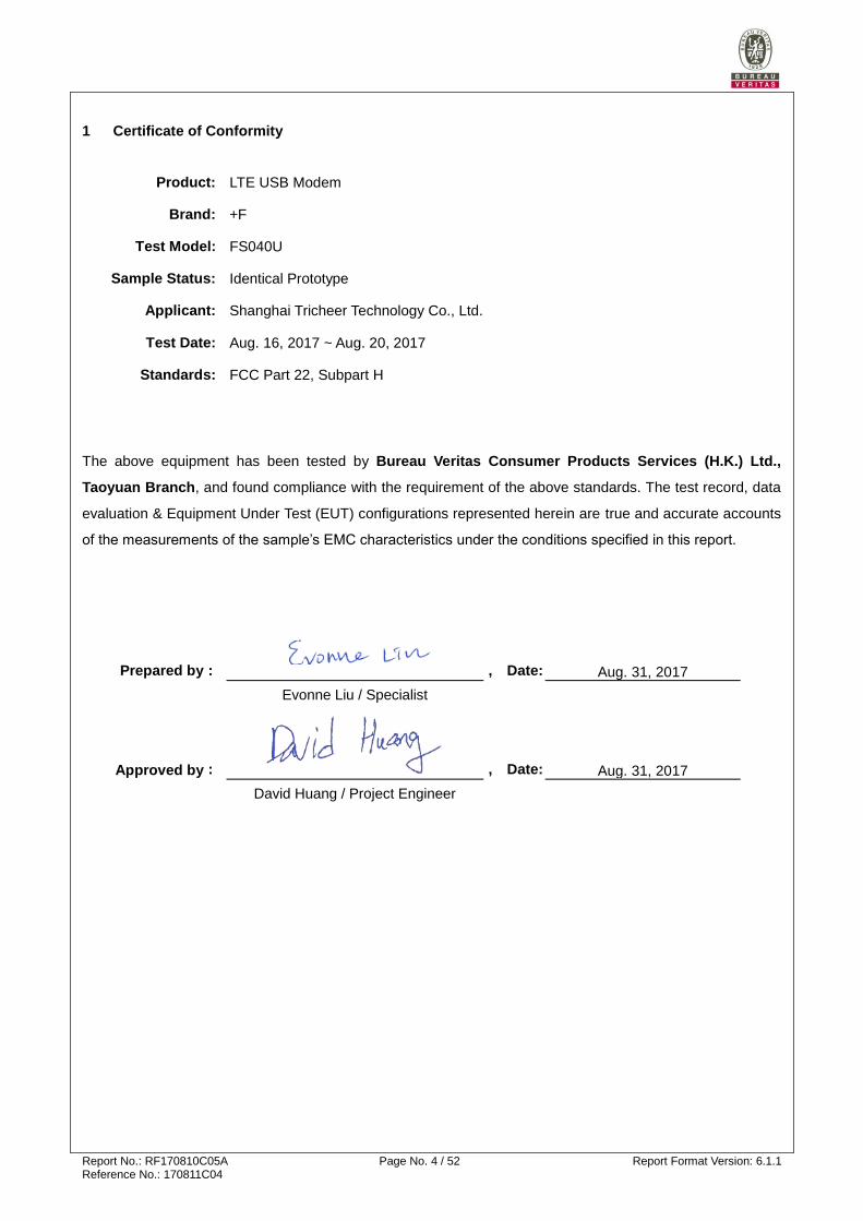
1 Certificate of Conformity
Product: LTE USB Modem
Brand: +F
Test Model: FS040U
Sample Status: Identical Prototype
Applicant: Shanghai Tricheer Technology Co., Ltd.
Test Date: Aug. 16, 2017 ~ Aug. 20, 2017
Standards: FCC Part 22, Subpart H
The above equipment has been tested by Bureau Veritas Consumer Products Services (H.K.) Ltd.,
Taoyuan Branch, and found compliance with the requirement of the above standards. The test record, data
evaluation & Equipment Under Test (EUT) configurations represented herein are true and accurate accounts
of the measurements of the sample’s EMC characteristics under the conditions specified in this report.
Prepared by :
, Date: Aug. 31, 2017
Evonne Liu / Specialist
Approved by
:
, Date: Aug. 31, 2017
David Huang / Project Engineer
Report No.: RF170810C05A Page No. 5 / 52 Report Format Version: 6.1.1 Reference No.: 170811C04
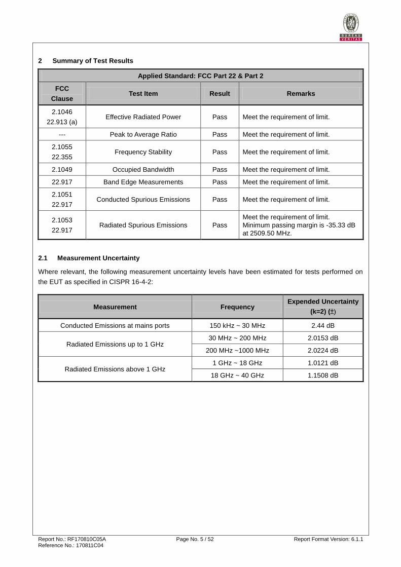
2 Summary of Test Results
Applied Standard: FCC Part 22 & Part 2
FCC
Clause Test Item Result Remarks
2.1046
22.913 (a) Effective Radiated Power Pass Meet the requirement of limit.
--- Peak to Average Ratio Pass Meet the requirement of limit.
2.1055
22.355 Frequency Stability Pass Meet the requirement of limit.
2.1049 Occupied Bandwidth Pass Meet the requirement of limit.
22.917 Band Edge Measurements Pass Meet the requirement of limit.
2.1051
22.917 Conducted Spurious Emissions Pass Meet the requirement of limit.
2.1053
22.917 Radiated Spurious Emissions Pass
Meet the requirement of limit.
Minimum passing margin is -35.33 dB
at 2509.50 MHz.
2.1 Measurement Uncertainty
Where relevant, the following measurement uncertainty levels have been estimated for tests performed on
the EUT as specified in CISPR 16-4-2:
Measurement Frequency Expended Uncertainty
(k=2) (±)
Conducted Emissions at mains ports 150 kHz ~ 30 MHz 2.44 dB
Radiated Emissions up to 1 GHz 30 MHz ~ 200 MHz 2.0153 dB
200 MHz ~1000 MHz 2.0224 dB
Radiated Emissions above 1 GHz 1 GHz ~ 18 GHz 1.0121 dB
18 GHz ~ 40 GHz 1.1508 dB
Report No.: RF170810C05A Page No. 6 / 52 Report Format Version: 6.1.1 Reference No.: 170811C04
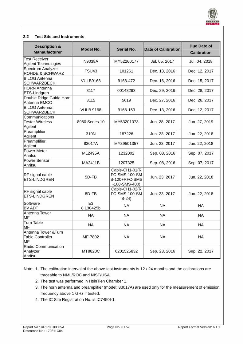
2.2 Test Site and Instruments
Description &
Manaufacturer Model No. Serial No. Date of Calibration
Due Date of
Calibration
Test Receiver Agilent Technologies
N9038A MY52260177 Jul. 05, 2017 Jul. 04, 2018
Spectrum Analyzer ROHDE & SCHWARZ
FSU43 101261 Dec. 13, 2016 Dec. 12, 2017
BILOG Antenna SCHWARZBECK
VULB9168 9168-472 Dec. 16, 2016 Dec. 15, 2017
HORN Antenna ETS-Lindgren
3117 00143293 Dec. 29, 2016 Dec. 28, 2017
Double Ridge Guide Horn Antenna EMCO
3115 5619 Dec. 27, 2016 Dec. 26, 2017
BILOG Antenna SCHWARZBECK
VULB 9168 9168-153 Dec. 13, 2016 Dec. 12, 2017
Communications Tester-Wireless Agilent
8960 Series 10 MY53201073 Jun. 28, 2017 Jun. 27, 2019
Preamplifier Agilent
310N 187226 Jun. 23, 2017 Jun. 22, 2018
Preamplifier Agilent
83017A MY39501357 Jun. 23, 2017 Jun. 22, 2018
Power Meter Anritsu
ML2495A 1232002 Sep. 08, 2016 Sep. 07, 2017
Power Sensor Anritsu
MA2411B 1207325 Sep. 08, 2016 Sep. 07, 2017
RF signal cable ETS-LINDGREN
5D-FB
Cable-CH1-01(RFC-SMS-100-SMS-120+RFC-SMS-100-SMS-400)
Jun. 23, 2017 Jun. 22, 2018
RF signal cable ETS-LINDGREN
8D-FB Cable-CH1-02(RFC-SMS-100-SM
S-24) Jun. 23, 2017 Jun. 22, 2018
Software BV ADT
E3 8.130425b
NA NA NA
Antenna Tower MF
NA NA NA NA
Turn Table MF
NA NA NA NA
Antenna Tower &Turn Table Controller MF
MF-7802 NA NA NA
Radio Communication Analyzer Anritsu
MT8820C 6201525832 Sep. 23, 2016 Sep. 22, 2017
Note: 1. The calibration interval of the above test instruments is 12 / 24 months and the calibrations are
traceable to NML/ROC and NIST/USA.
2. The test was performed in HsinTien Chamber 1.
3. The horn antenna and preamplifier (model: 83017A) are used only for the measurement of emission
frequency above 1 GHz if tested.
4. The IC Site Registration No. is IC7450I-1.
Report No.: RF170810C05A Page No. 7 / 52 Report Format Version: 6.1.1 Reference No.: 170811C04
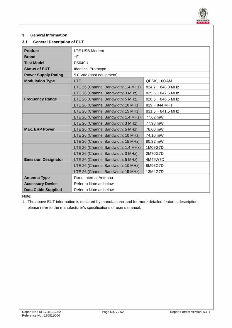
3 General Information
3.1 General Description of EUT
Product LTE USB Modem
Brand +F
Test Model FS040U
Status of EUT Identical Prototype
Power Supply Rating 5.0 Vdc (host equipment)
Modulation Type LTE QPSK, 16QAM
Frequency Range
LTE 26 (Channel Bandwidth: 1.4 MHz) 824.7 ~ 848.3 MHz
LTE 26 (Channel Bandwidth: 3 MHz) 825.5 ~ 847.5 MHz
LTE 26 (Channel Bandwidth: 5 MHz) 826.5 ~ 846.5 MHz
LTE 26 (Channel Bandwidth: 10 MHz) 829 ~ 844 MHz
LTE 26 (Channel Bandwidth: 15 MHz) 831.5 ~ 841.5 MHz
Max. ERP Power
LTE 26 (Channel Bandwidth: 1.4 MHz) 77.62 mW
LTE 26 (Channel Bandwidth: 3 MHz) 77.98 mW
LTE 26 (Channel Bandwidth: 5 MHz) 76.00 mW
LTE 26 (Channel Bandwidth: 10 MHz) 74.10 mW
LTE 26 (Channel Bandwidth: 15 MHz) 80.32 mW
Emission Designator
LTE 26 (Channel Bandwidth: 1.4 MHz) 1M09G7D
LTE 26 (Channel Bandwidth: 3 MHz) 2M70G7D
LTE 26 (Channel Bandwidth: 5 MHz) 4M49W7D
LTE 26 (Channel Bandwidth: 10 MHz) 8M95G7D
LTE 26 (Channel Bandwidth: 15 MHz) 13M4G7D
Antenna Type Fixed Internal Antenna
Accessory Device Refer to Note as below
Data Cable Supplied Refer to Note as below
Note:
1. The above EUT information is declared by manufacturer and for more detailed features description,
please refer to the manufacturer's specifications or user's manual.
Report No.: RF170810C05A Page No. 8 / 52 Report Format Version: 6.1.1 Reference No.: 170811C04
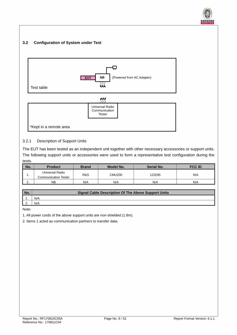
3.2 Configuration of System under Test
3.2.1 Description of Support Units
The EUT has been tested as an independent unit together with other necessary accessories or support units.
The following support units or accessories were used to form a representative test configuration during the
tests.
No. Product Brand Model No. Serial No. FCC ID
1. Universal Radio
Communication Tester R&S CMU200 123295 N/A
2. NB N/A N/A N/A N/A
No. Signal Cable Description Of The Above Support Units
1. N/A
2. N/A
Note:
1. All power cords of the above support units are non-shielded (1.8m).
2. Items 1 acted as communication partners to transfer data.
Test table
(Powered from AC Adapter)
Universal Radio Communication
Tester
*Kept in a remote area
NB EUT
Report No.: RF170810C05A Page No. 9 / 52 Report Format Version: 6.1.1 Reference No.: 170811C04
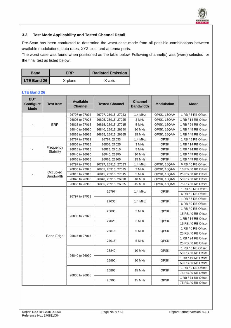
3.3 Test Mode Applicability and Tested Channel Detail
Pre-Scan has been conducted to determine the worst-case mode from all possible combinations between
available modulations, data rates, XYZ axis, and antenna ports.
The worst case was found when positioned as the table below. Following channel(s) was (were) selected for
the final test as listed below:
Band ERP Radiated Emission
LTE Band 26 X-plane X-axis
LTE Band 26
EUT
Configure
Mode
Test Item Available
Channel Tested Channel
Channel
Bandwidth Modulation Mode
- ERP
26797 to 27033 26797, 26915, 27033 1.4 MHz QPSK, 16QAM 1 RB / 5 RB Offset
26805 to 27025 26805, 26915, 27025 3 MHz QPSK, 16QAM 1 RB / 14 RB Offset
26815 to 27015 26815, 26915, 27015 5 MHz QPSK, 16QAM 1 RB / 24 RB Offset
26840 to 26990 26840, 26915, 26990 10 MHz QPSK, 16QAM 1 RB / 49 RB Offset
26865 to 26965 26865, 26915, 26965 15 MHz QPSK, 16QAM 1 RB / 49 RB Offset
- Frequency
Stability
26797 to 27033 26797, 27033 1.4 MHz QPSK 1 RB / 5 RB Offset
26805 to 27025 26805, 27025 3 MHz QPSK 1 RB / 14 RB Offset
26815 to 27015 26815, 27015 5 MHz QPSK 1 RB / 24 RB Offset
26840 to 26990 26840, 26990 10 MHz QPSK 1 RB / 49 RB Offset
26865 to 26965 26865, 26965 15 MHz QPSK 1 RB / 49 RB Offset
- Occupied Bandwidth
26797 to 27033 26797, 26915, 27033 1.4 MHz QPSK, 16QAM 6 RB / 0 RB Offset
26805 to 27025 26805, 26915, 27025 3 MHz QPSK, 16QAM 15 RB / 0 RB Offset
26815 to 27015 26815, 26915, 27015 5 MHz QPSK, 16QAM 25 RB / 0 RB Offset
26840 to 26990 26840, 26915, 26990 10 MHz QPSK, 16QAM 50 RB / 0 RB Offset
26865 to 26965 26865, 26915, 26965 15 MHz QPSK, 16QAM 75 RB / 0 RB Offset
- Band Edge
26797 to 27033
26797 1.4 MHz QPSK 1 RB / 0 RB Offset
6 RB / 0 RB Offset
27033 1.4 MHz QPSK 1 RB / 5 RB Offset
6 RB / 0 RB Offset
26805 to 27025
26805 3 MHz QPSK 1 RB / 0 RB Offset
15 RB / 0 RB Offset
27025 3 MHz QPSK 1 RB / 14 RB Offset
15 RB / 0 RB Offset
26815 to 27015
26815 5 MHz QPSK 1 RB / 0 RB Offset
25 RB / 0 RB Offset
27015 5 MHz QPSK 1 RB / 24 RB Offset
25 RB / 0 RB Offset
26840 to 26990
26840 10 MHz QPSK 1 RB / 0 RB Offset
50 RB / 0 RB Offset
26990 10 MHz QPSK 1 RB / 49 RB Offset
50 RB / 0 RB Offset
26865 to 26965
26865 15 MHz QPSK 1 RB / 0 RB Offset
75 RB / 0 RB Offset
26965 15 MHz QPSK 1 RB / 74 RB Offset
75 RB / 0 RB Offset
Report No.: RF170810C05A Page No. 10 / 52 Report Format Version: 6.1.1 Reference No.: 170811C04
EUT
Configure
Mode
Test Item Available
Channel Tested Channel
Channel
Bandwidth Modulation Mode
- Peak to
Average Ratio
26797 to 27033 26797, 26915, 27033 1.4 MHz QPSK, 16QAM 1 RB / 0 RB Offset
26805 to 27025 26805, 26915, 27025 3 MHz QPSK, 16QAM 15 RB / 0 RB Offset
26815 to 27015 26815, 26915, 27015 5 MHz QPSK, 16QAM 25 RB / 0 RB Offset
26840 to 26990 26840, 26915, 26990 10 MHz QPSK, 16QAM 50 RB / 0 RB Offset
26865 to 26965 26865, 26915, 26965 15 MHz QPSK, 16QAM 75 RB / 0 RB Offset
- Conducted Emission
26797 to 27033 26797, 26915, 27033 1.4 MHz QPSK 1 RB / 0 RB Offset
26805 to 27025 26805, 26915, 27025 3 MHz QPSK 15 RB / 0 RB Offset
26815 to 27015 26815, 26915, 27015 5 MHz QPSK 25 RB / 0 RB Offset
26840 to 26990 26840, 26915, 26990 10 MHz QPSK 1 RB / 0 RB Offset
26865 to 26965 26865, 26915, 26965 15 MHz QPSK 25 RB / 0 RB Offset
- Radiated Emission
26865 to 26965 26865, 26915, 26965 15 MHz QPSK 1 RB / 0 RB Offset
Note: This device was tested under all bandwidths, RB configurations and modulations. The worst case was
found in QPSK modulation.
Test Condition:
Test Item Environmental Conditions Input Power Tested By
ERP 25 deg. C, 65 % RH 4.5 Vdc Carlos Chen
Frequency Stability 25 deg. C, 65 % RH 4.5 Vdc Carlos Chen
Occupied Bandwidth 25 deg. C, 65 % RH 4.5 Vdc Carlos Chen
Band Edge 25 deg. C, 65 % RH 4.5 Vdc Carlos Chen
Peak to Average Ratio 25 deg. C, 65 % RH 4.5 Vdc Carlos Chen
Condcudeted Emission 25 deg. C, 65 % RH 4.5 Vdc Carlos Chen
Radiated Emission 25 deg. C, 65 % RH 120 Vac, 60 Hz Charles Hsiao
3.4 EUT Operating Conditions
The EUT makes a call to the communication simulator. The communication simulator station system
controlled a EUT to export maximum output power under transmission mode and specific channel frequency.
3.5 General Description of Applied Standards
The EUT is a RF Product. According to the specifications of the manufacturer, it must comply with the
requirements of the following standards:
FCC 47 CFR Part 2
FCC 47 CFR Part 22
KDB 971168 D01 Power Meas License Digital Systems v02r02
ANSI/TIA/EIA-603-D 2010
Note: All test items have been performed and recorded as per the above standards.
Report No.: RF170810C05A Page No. 11 / 52 Report Format Version: 6.1.1 Reference No.: 170811C04
4 Test Types and Results
4.1 Output Power Measurement
4.1.1 Limits of Output Power Measurement
Mobile / Portable station are limited to 7 watts e.r.p.
4.1.2 Test Procedures
EIRP / ERP Measurement:
a. All measurements were done at low, middle and high operational frequency range. RBW and VBW is 1
MHz for GSM, GPRS & EDGE, and 5 MHz for WCDMA and CDMA, and 10 MHz for LTE mode.
b. Substitution method is used for E.I.R.P measurement. In the semi-anechoic chamber, EUT placed on the
0.8 m height of Turn Table, rotated the table around 360 degrees to search the maximum radiation power
and receiver antenna shall be rotated vertical and horizontal polarization and moved height from 1 m to 4
m to find the maximum polar radiated power. The “Read Value” is the spectrum reading the maximum
power value.
c. The substitution horn antenna is substituted for EUT at the same position and signals generator export the
CW signal to the substitution antenna via a tx cable. Rotated the Turn Table and moved receiving antenna
to find the maximum radiation power. Adjust output power level of S.G to get a Value of spectrum reading
equal to “Read Value” of step b. Record the power level of S.G.
d. EIRP = Output power level of S.G – TX cable loss + Antenna gain of substitution horn.E.R.P power can
be calculated form E.I.R.P power by subtracting the gain of dipole, E.R.P power = E.I.P.R power - 2.15
dBi.
Conducted Power Measurement:
The EUT was set up for the maximum power with GSM, GPRS, EDGE, WCDMA, CDMA, and LTE link data
modulation and link up with simulator. Set the EUT to transmit under low, middle and high channel and record
the power level shown on simulator.
Report No.: RF170810C05A Page No. 12 / 52 Report Format Version: 6.1.1 Reference No.: 170811C04
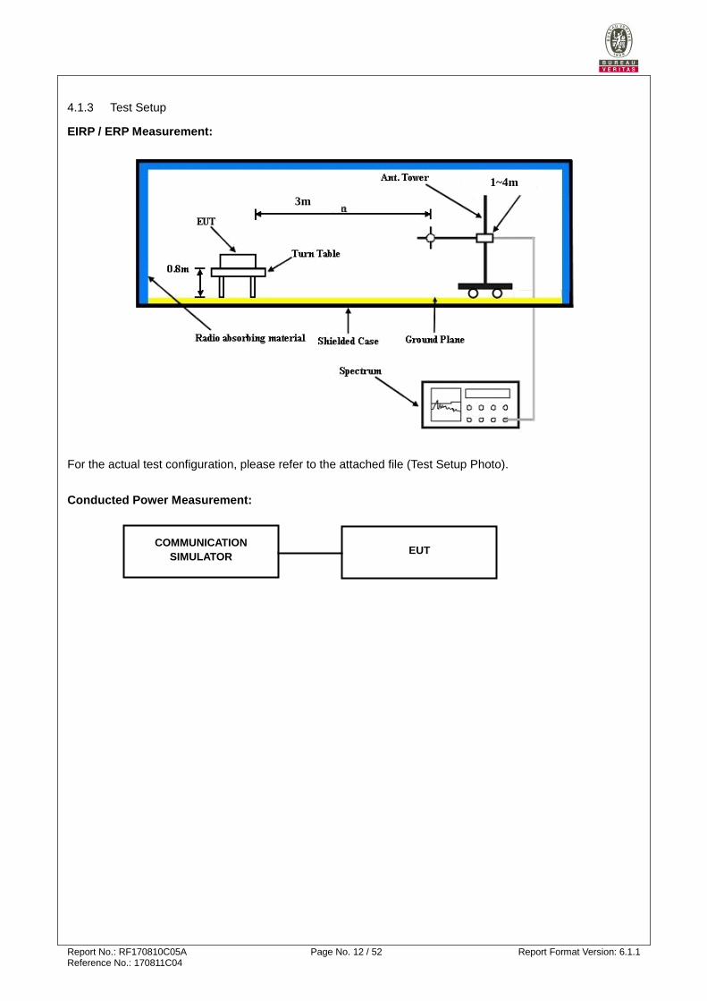
4.1.3 Test Setup
EIRP / ERP Measurement:
For the actual test configuration, please refer to the attached file (Test Setup Photo).
Conducted Power Measurement:
3m
1~4m
COMMUNICATION
SIMULATOR EUT
Report No.: RF170810C05A Page No. 13 / 52 Report Format Version: 6.1.1 Reference No.: 170811C04
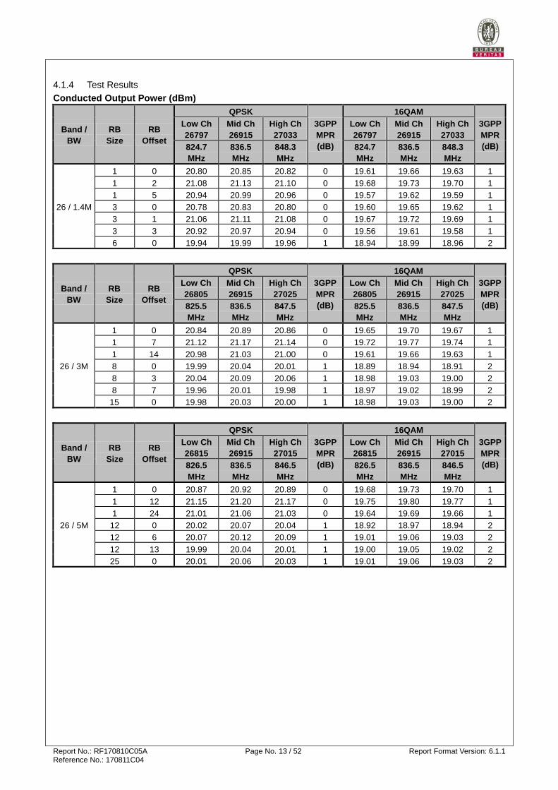
4.1.4 Test Results
Conducted Output Power (dBm)
Band /
BW
RB
Size
RB
Offset
QPSK
3GPP
MPR
(dB)
16QAM
3GPP
MPR
(dB)
Low Ch
26797
Mid Ch
26915
High Ch
27033
Low Ch
26797
Mid Ch
26915
High Ch
27033
824.7
MHz
836.5
MHz
848.3
MHz
824.7
MHz
836.5
MHz
848.3
MHz
26 / 1.4M
1 0 20.80 20.85 20.82 0 19.61 19.66 19.63 1
1 2 21.08 21.13 21.10 0 19.68 19.73 19.70 1
1 5 20.94 20.99 20.96 0 19.57 19.62 19.59 1
3 0 20.78 20.83 20.80 0 19.60 19.65 19.62 1
3 1 21.06 21.11 21.08 0 19.67 19.72 19.69 1
3 3 20.92 20.97 20.94 0 19.56 19.61 19.58 1
6 0 19.94 19.99 19.96 1 18.94 18.99 18.96 2
Band /
BW
RB
Size
RB
Offset
QPSK
3GPP
MPR
(dB)
16QAM
3GPP
MPR
(dB)
Low Ch
26805
Mid Ch
26915
High Ch
27025
Low Ch
26805
Mid Ch
26915
High Ch
27025
825.5
MHz
836.5
MHz
847.5
MHz
825.5
MHz
836.5
MHz
847.5
MHz
26 / 3M
1 0 20.84 20.89 20.86 0 19.65 19.70 19.67 1
1 7 21.12 21.17 21.14 0 19.72 19.77 19.74 1
1 14 20.98 21.03 21.00 0 19.61 19.66 19.63 1
8 0 19.99 20.04 20.01 1 18.89 18.94 18.91 2
8 3 20.04 20.09 20.06 1 18.98 19.03 19.00 2
8 7 19.96 20.01 19.98 1 18.97 19.02 18.99 2
15 0 19.98 20.03 20.00 1 18.98 19.03 19.00 2
Band /
BW
RB
Size
RB
Offset
QPSK
3GPP
MPR
(dB)
16QAM
3GPP
MPR
(dB)
Low Ch
26815
Mid Ch
26915
High Ch
27015
Low Ch
26815
Mid Ch
26915
High Ch
27015
826.5
MHz
836.5
MHz
846.5
MHz
826.5
MHz
836.5
MHz
846.5
MHz
26 / 5M
1 0 20.87 20.92 20.89 0 19.68 19.73 19.70 1
1 12 21.15 21.20 21.17 0 19.75 19.80 19.77 1
1 24 21.01 21.06 21.03 0 19.64 19.69 19.66 1
12 0 20.02 20.07 20.04 1 18.92 18.97 18.94 2
12 6 20.07 20.12 20.09 1 19.01 19.06 19.03 2
12 13 19.99 20.04 20.01 1 19.00 19.05 19.02 2
25 0 20.01 20.06 20.03 1 19.01 19.06 19.03 2
Report No.: RF170810C05A Page No. 14 / 52 Report Format Version: 6.1.1 Reference No.: 170811C04
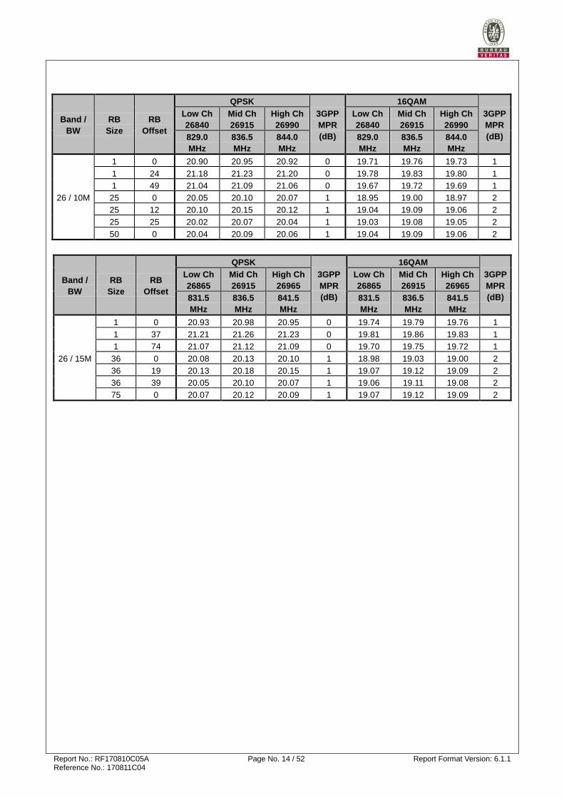
Band /
BW
RB
Size
RB
Offset
QPSK
3GPP
MPR
(dB)
16QAM
3GPP
MPR
(dB)
Low Ch
26840
Mid Ch
26915
High Ch
26990
Low Ch
26840
Mid Ch
26915
High Ch
26990
829.0
MHz
836.5
MHz
844.0
MHz
829.0
MHz
836.5
MHz
844.0
MHz
26 / 10M
1 0 20.90 20.95 20.92 0 19.71 19.76 19.73 1
1 24 21.18 21.23 21.20 0 19.78 19.83 19.80 1
1 49 21.04 21.09 21.06 0 19.67 19.72 19.69 1
25 0 20.05 20.10 20.07 1 18.95 19.00 18.97 2
25 12 20.10 20.15 20.12 1 19.04 19.09 19.06 2
25 25 20.02 20.07 20.04 1 19.03 19.08 19.05 2
50 0 20.04 20.09 20.06 1 19.04 19.09 19.06 2
Band /
BW
RB
Size
RB
Offset
QPSK
3GPP
MPR
(dB)
16QAM
3GPP
MPR
(dB)
Low Ch
26865
Mid Ch
26915
High Ch
26965
Low Ch
26865
Mid Ch
26915
High Ch
26965
831.5
MHz
836.5
MHz
841.5
MHz
831.5
MHz
836.5
MHz
841.5
MHz
26 / 15M
1 0 20.93 20.98 20.95 0 19.74 19.79 19.76 1
1 37 21.21 21.26 21.23 0 19.81 19.86 19.83 1
1 74 21.07 21.12 21.09 0 19.70 19.75 19.72 1
36 0 20.08 20.13 20.10 1 18.98 19.03 19.00 2
36 19 20.13 20.18 20.15 1 19.07 19.12 19.09 2
36 39 20.05 20.10 20.07 1 19.06 19.11 19.08 2
75 0 20.07 20.12 20.09 1 19.07 19.12 19.09 2
Report No.: RF170810C05A Page No. 15 / 52 Report Format Version: 6.1.1 Reference No.: 170811C04
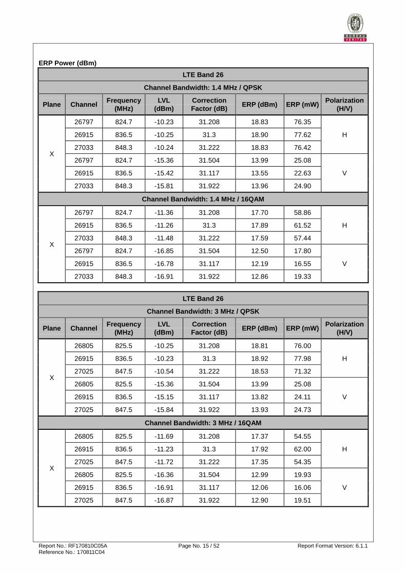
ERP Power (dBm)
LTE Band 26
Channel Bandwidth: 1.4 MHz / QPSK
Plane Channel Frequency
(MHz)
LVL
(dBm)
Correction
Factor (dB) ERP (dBm) ERP (mW)
Polarization
(H/V)
X
26797 824.7 -10.23 31.208 18.83 76.35
H 26915 836.5 -10.25 31.3 18.90 77.62
27033 848.3 -10.24 31.222 18.83 76.42
26797 824.7 -15.36 31.504 13.99 25.08
V 26915 836.5 -15.42 31.117 13.55 22.63
27033 848.3 -15.81 31.922 13.96 24.90
Channel Bandwidth: 1.4 MHz / 16QAM
X
26797 824.7 -11.36 31.208 17.70 58.86
H 26915 836.5 -11.26 31.3 17.89 61.52
27033 848.3 -11.48 31.222 17.59 57.44
26797 824.7 -16.85 31.504 12.50 17.80
V 26915 836.5 -16.78 31.117 12.19 16.55
27033 848.3 -16.91 31.922 12.86 19.33
LTE Band 26
Channel Bandwidth: 3 MHz / QPSK
Plane Channel Frequency
(MHz)
LVL
(dBm)
Correction
Factor (dB) ERP (dBm) ERP (mW)
Polarization
(H/V)
X
26805 825.5 -10.25 31.208 18.81 76.00
H 26915 836.5 -10.23 31.3 18.92 77.98
27025 847.5 -10.54 31.222 18.53 71.32
26805 825.5 -15.36 31.504 13.99 25.08
V 26915 836.5 -15.15 31.117 13.82 24.11
27025 847.5 -15.84 31.922 13.93 24.73
Channel Bandwidth: 3 MHz / 16QAM
X
26805 825.5 -11.69 31.208 17.37 54.55
H 26915 836.5 -11.23 31.3 17.92 62.00
27025 847.5 -11.72 31.222 17.35 54.35
26805 825.5 -16.36 31.504 12.99 19.93
V 26915 836.5 -16.91 31.117 12.06 16.06
27025 847.5 -16.87 31.922 12.90 19.51
Report No.: RF170810C05A Page No. 16 / 52 Report Format Version: 6.1.1 Reference No.: 170811C04
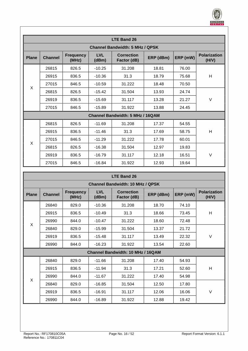
LTE Band 26
Channel Bandwidth: 5 MHz / QPSK
Plane Channel Frequency
(MHz)
LVL
(dBm)
Correction
Factor (dB) ERP (dBm) ERP (mW)
Polarization
(H/V)
X
26815 826.5 -10.25 31.208 18.81 76.00
H 26915 836.5 -10.36 31.3 18.79 75.68
27015 846.5 -10.59 31.222 18.48 70.50
26815 826.5 -15.42 31.504 13.93 24.74
V 26919 836.5 -15.69 31.117 13.28 21.27
27015 846.5 -15.89 31.922 13.88 24.45
Channel Bandwidth: 5 MHz / 16QAM
X
26815 826.5 -11.69 31.208 17.37 54.55
H 26915 836.5 -11.46 31.3 17.69 58.75
27015 846.5 -11.29 31.222 17.78 60.01
26815 826.5 -16.38 31.504 12.97 19.83
V 26919 836.5 -16.79 31.117 12.18 16.51
27015 846.5 -16.84 31.922 12.93 19.64
LTE Band 26
Channel Bandwidth: 10 MHz / QPSK
Plane Channel Frequency
(MHz)
LVL
(dBm)
Correction
Factor (dB) ERP (dBm) ERP (mW)
Polarization
(H/V)
X
26840 829.0 -10.36 31.208 18.70 74.10
H 26915 836.5 -10.49 31.3 18.66 73.45
26990 844.0 -10.47 31.222 18.60 72.48
26840 829.0 -15.99 31.504 13.37 21.72
V 26919 836.5 -15.48 31.117 13.49 22.32
26990 844.0 -16.23 31.922 13.54 22.60
Channel Bandwidth: 10 MHz / 16QAM
X
26840 829.0 -11.66 31.208 17.40 54.93
H 26915 836.5 -11.94 31.3 17.21 52.60
26990 844.0 -11.67 31.222 17.40 54.98
26840 829.0 -16.85 31.504 12.50 17.80
V 26919 836.5 -16.91 31.117 12.06 16.06
26990 844.0 -16.89 31.922 12.88 19.42
Report No.: RF170810C05A Page No. 17 / 52 Report Format Version: 6.1.1 Reference No.: 170811C04
LTE Band 26
Channel Bandwidth: 15 MHz / QPSK
Plane Channel Frequency
(MHz)
LVL
(dBm)
Correction
Factor (dB) ERP (dBm) ERP (mW)
Polarization
(H/V)
X
26865 831.5 -10.01 31.208 19.05 80.32
H 26915 836.5 -10.75 31.3 18.40 69.18
26965 841.5 -10.49 31.222 18.58 72.14
26865 831.5 -15.48 31.504 13.87 24.40
V 26915 836.5 -15.76 31.117 13.21 20.93
26965 841.5 -15.98 31.922 13.79 23.94
Channel Bandwidth: 15 MHz / 16QAM
X
26865 831.5 -11.04 31.208 18.02 63.42
H 26915 836.5 -11.20 31.3 17.95 62.37
26965 841.5 -11.58 31.222 17.49 56.13
26865 831.5 -16.36 31.504 12.99 19.93
V 26915 836.5 -16.85 31.117 12.12 16.28
26965 841.5 -16.99 31.922 12.78 18.98
Report No.: RF170810C05A Page No. 18 / 52 Report Format Version: 6.1.1 Reference No.: 170811C04
4.2 Frequency Stability Measurement
4.2.1 Limits of Frequency Stabiliity Measurement
1.5 ppm is for base and fixed station. 2.5 ppm is for mobile station.
4.2.2 Test Procedure
a. Device is placed at the oven room. The oven room could control the temperatures and humidity. Power
warm up is at least 15 min and power applied should perform before recording frequency error.
b. EUT is connected the external power supply to control the DC input power. The test voltage range is from
minimum to maximum working voltage. Each step shall be record the frequency error rate.
c. The temperature range step is 10 degrees in this test items. All temperature levels shall be hold the ±0.5
℃ during the measurement testing. The each temperature step shall be at least 0.5 hours, consider the
EUT could be test under the stability condition.
NOTE: The frequency error was recorded frequency error from the communication simulator.
4.2.3 Test Setup
Communication
Simulator
DC Power Supply
Oven Room
Antenna
External Power Source
EUT
Report No.: RF170810C05A Page No. 19 / 52 Report Format Version: 6.1.1 Reference No.: 170811C04
4.2.4 Test Results
Frequency Error vs. Voltage
Voltage
(Volts)
LTE Band 26
Limit (ppm)
Channel Bandwidth: 1.4 MHz
Low Channel High Channel
Frequency (MHz) Frequency Error
(ppm) Frequency (MHz)
Frequency Error
(ppm)
5.0 824.700004 0.004 848.300001 0.002 2.5
4.5 824.700004 0.005 848.300002 0.002 2.5
5.5 824.700002 0.003 848.300001 0.002 2.5
Note: The applicant defined the normal working voltage of the battery is from 4.5 Vdc to 5.5 Vdc.
Frequency Error vs. Temperature
Temp. (℃)
LTE Band 26
Limit (ppm)
Channel Bandwidth: 1.4 MHz
Low Channel High Channel
Frequency (MHz) Frequency Error
(ppm) Frequency (MHz)
Frequency Error
(ppm)
-20 824.700004 0.005 848.300002 0.003 2.5
-10 824.700002 0.002 848.300004 0.004 2.5
0 824.700004 0.005 848.300001 0.001 2.5
10 824.700002 0.003 848.300001 0.001 2.5
20 824.699999 -0.002 848.299998 -0.002 2.5
30 824.699997 -0.004 848.299998 -0.002 2.5
40 824.699997 -0.004 848.299998 -0.003 2.5
50 824.699998 -0.003 848.299998 -0.002 2.5
55 824.699997 -0.003 848.299996 -0.004 2.5

Report No.: RF170810C05A Page No. 20 / 52 Report Format Version: 6.1.1 Reference No.: 170811C04
Frequency Error vs. Voltage
Voltage
(Volts)
LTE Band 26
Limit (ppm)
Channel Bandwidth: 3 MHz
Low Channel High Channel
Frequency (MHz) Frequency Error
(ppm) Frequency (MHz)
Frequency Error
(ppm)
5.0 825.500003 0.004 847.500000 0.000 2.5
4.5 825.500004 0.005 847.500000 0.000 2.5
5.5 825.500002 0.002 847.500000 0.000 2.5
Note: The applicant defined the normal working voltage of the battery is from 4.5 Vdc to 5.5 Vdc.
Frequency Error vs. Temperature
Temp. (℃)
LTE Band 26
Limit (ppm)
Channel Bandwidth: 3 MHz
Low Channel High Channel
Frequency (MHz) Frequency Error
(ppm) Frequency (MHz)
Frequency Error
(ppm)
-20 825.500002 0.002 847.500003 0.003 2.5
-10 825.500002 0.003 847.500004 0.004 2.5
0 825.500002 0.003 847.500002 0.002 2.5
10 825.500003 0.003 847.500004 0.004 2.5
20 825.499997 -0.004 847.499997 -0.004 2.5
30 825.499999 -0.002 847.499997 -0.004 2.5
40 825.499998 -0.002 847.499998 -0.003 2.5
50 825.499996 -0.004 847.499997 -0.003 2.5
55 825.499998 -0.003 847.499998 -0.003 2.5
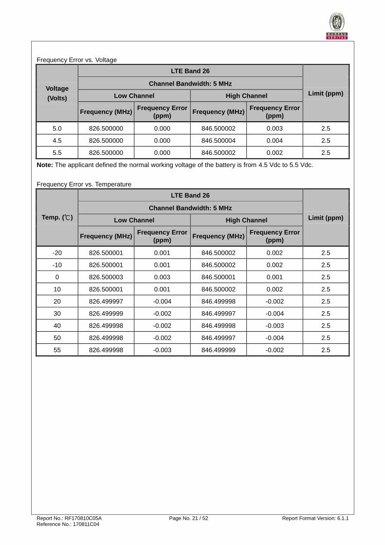
Report No.: RF170810C05A Page No. 21 / 52 Report Format Version: 6.1.1 Reference No.: 170811C04
Frequency Error vs. Voltage
Voltage
(Volts)
LTE Band 26
Limit (ppm)
Channel Bandwidth: 5 MHz
Low Channel High Channel
Frequency (MHz) Frequency Error
(ppm) Frequency (MHz)
Frequency Error
(ppm)
5.0 826.500000 0.000 846.500002 0.003 2.5
4.5 826.500000 0.000 846.500004 0.004 2.5
5.5 826.500000 0.000 846.500002 0.002 2.5
Note: The applicant defined the normal working voltage of the battery is from 4.5 Vdc to 5.5 Vdc.
Frequency Error vs. Temperature
Temp. (℃)
LTE Band 26
Limit (ppm)
Channel Bandwidth: 5 MHz
Low Channel High Channel
Frequency (MHz) Frequency Error
(ppm) Frequency (MHz)
Frequency Error
(ppm)
-20 826.500001 0.001 846.500002 0.002 2.5
-10 826.500001 0.001 846.500002 0.002 2.5
0 826.500003 0.003 846.500001 0.001 2.5
10 826.500001 0.001 846.500002 0.002 2.5
20 826.499997 -0.004 846.499998 -0.002 2.5
30 826.499999 -0.002 846.499997 -0.004 2.5
40 826.499998 -0.002 846.499998 -0.003 2.5
50 826.499998 -0.002 846.499997 -0.004 2.5
55 826.499998 -0.003 846.499999 -0.002 2.5

Report No.: RF170810C05A Page No. 22 / 52 Report Format Version: 6.1.1 Reference No.: 170811C04
Frequency Error vs. Voltage
Voltage
(Volts)
LTE Band 26
Limit (ppm)
Channel Bandwidth: 10 MHz
Low Channel High Channel
Frequency (MHz) Frequency Error
(ppm) Frequency (MHz)
Frequency Error
(ppm)
5.0 829.000004 0.005 844.000003 0.004 2.5
4.5 829.000002 0.002 844.000002 0.003 2.5
5.5 829.000003 0.004 844.000003 0.003 2.5
Note: The applicant defined the normal working voltage of the battery is from 4.5 Vdc to 5.5 Vdc.
Frequency Error vs. Temperature
Temp. (℃)
LTE Band 26
Limit (ppm)
Channel Bandwidth: 10 MHz
Low Channel High Channel
Frequency (MHz) Frequency Error
(ppm) Frequency (MHz)
Frequency Error
(ppm)
-20 829.000001 0.002 844.000001 0.001 2.5
-10 829.000002 0.002 844.000001 0.002 2.5
0 829.000003 0.003 844.000002 0.002 2.5
10 829.000002 0.003 844.000004 0.004 2.5
20 828.999996 -0.004 843.999998 -0.003 2.5
30 828.999998 -0.003 843.999999 -0.002 2.5
40 828.999997 -0.004 843.999996 -0.005 2.5
50 828.999996 -0.005 843.999996 -0.005 2.5
55 828.999998 -0.002 843.999998 -0.002 2.5

Report No.: RF170810C05A Page No. 23 / 52 Report Format Version: 6.1.1 Reference No.: 170811C04
Frequency Error vs. Voltage
Voltage
(Volts)
LTE Band 26
Limit (ppm)
Channel Bandwidth: 15 MHz
Low Channel High Channel
Frequency (MHz) Frequency Error
(ppm) Frequency (MHz)
Frequency Error
(ppm)
5.0 831.500002 0.003 841.500003 0.003 2.5
4.5 831.500003 0.003 841.500002 0.002 2.5
5.5 831.500002 0.002 841.500003 0.004 2.5
Note: The applicant defined the normal working voltage of the battery is from 4.5 Vdc to 5.5 Vdc.
Frequency Error vs. Temperature
Temp. (℃)
LTE Band 26
Limit (ppm)
Channel Bandwidth: 15 MHz
Low Channel High Channel
Frequency (MHz) Frequency Error
(ppm) Frequency (MHz)
Frequency Error
(ppm)
-20 831.500002 0.002 841.500003 0.003 2.5
-10 831.500001 0.002 841.500002 0.002 2.5
0 831.500002 0.002 841.500004 0.004 2.5
10 831.500004 0.005 841.500002 0.002 2.5
20 831.499997 -0.004 841.499998 -0.002 2.5
30 831.499998 -0.002 841.499998 -0.002 2.5
40 831.499999 -0.002 841.499998 -0.003 2.5
50 831.499998 -0.002 841.499998 -0.002 2.5
55 831.499997 -0.004 841.499999 -0.002 2.5
Report No.: RF170810C05A Page No. 24 / 52 Report Format Version: 6.1.1 Reference No.: 170811C04
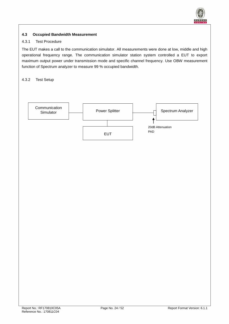
4.3 Occupied Bandwidth Measurement
4.3.1 Test Procedure
The EUT makes a call to the communication simulator. All measurements were done at low, middle and high
operational frequency range. The communication simulator station system controlled a EUT to export
maximum output power under transmission mode and specific channel frequency. Use OBW measurement
function of Spectrum analyzer to measure 99 % occupied bandwidth.
4.3.2 Test Setup
Communication
Simulator Spectrum Analyzer Power Splitter
EUT
20dB Attenuation
PAD
Report No.: RF170810C05A Page No. 25 / 52 Report Format Version: 6.1.1 Reference No.: 170811C04
4.3.3 Test Result
LTE Band 26
Channel Bandwidth: 1.4 MHz Channel Bandwidth: 3 MHz
Channel Frequency
(MHz)
99 % Occupied
Bandwidth (MHz) Channel Frequency
(MHz)
99 % Occupied
Bandwidth (MHz)
QPSK 16QAM QPSK 16QAM
26797 824.7 1.0877 1.0902 26805 825.5 2.7024 2.6975
26915 836.5 1.0890 1.0919 26915 836.5 2.7001 2.6977
27033 848.3 1.0908 1.0903 27025 847.5 2.7021 2.6969
Spectrum Plot of Worst Value
1.4 MHz / QPSK 1.4 MHz / 16QAM
3 MHz / QPSK 3 MHz / 16QAM
Report No.: RF170810C05A Page No. 26 / 52 Report Format Version: 6.1.1 Reference No.: 170811C04
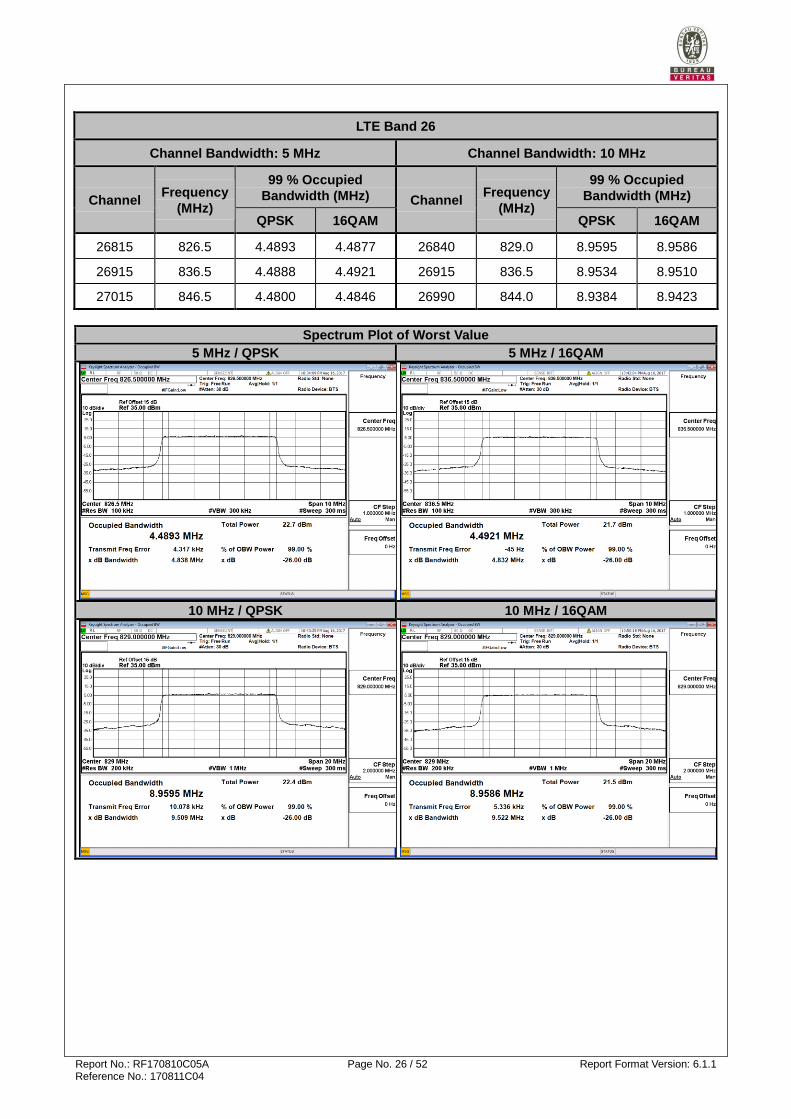
LTE Band 26
Channel Bandwidth: 5 MHz Channel Bandwidth: 10 MHz
Channel Frequency
(MHz)
99 % Occupied
Bandwidth (MHz) Channel Frequency
(MHz)
99 % Occupied
Bandwidth (MHz)
QPSK 16QAM QPSK 16QAM
26815 826.5 4.4893 4.4877 26840 829.0 8.9595 8.9586
26915 836.5 4.4888 4.4921 26915 836.5 8.9534 8.9510
27015 846.5 4.4800 4.4846 26990 844.0 8.9384 8.9423
Spectrum Plot of Worst Value
5 MHz / QPSK 5 MHz / 16QAM
10 MHz / QPSK 10 MHz / 16QAM
Report No.: RF170810C05A Page No. 27 / 52 Report Format Version: 6.1.1 Reference No.: 170811C04
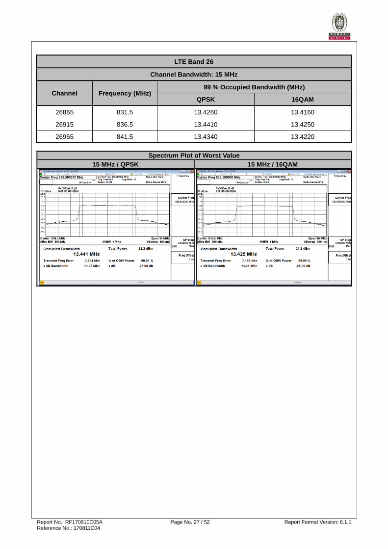
LTE Band 26
Channel Bandwidth: 15 MHz
Channel Frequency (MHz) 99 % Occupied Bandwidth (MHz)
QPSK 16QAM
26865 831.5 13.4260 13.4160
26915 836.5 13.4410 13.4250
26965 841.5 13.4340 13.4220
Spectrum Plot of Worst Value
15 MHz / QPSK 15 MHz / 16QAM
Report No.: RF170810C05A Page No. 28 / 52 Report Format Version: 6.1.1 Reference No.: 170811C04
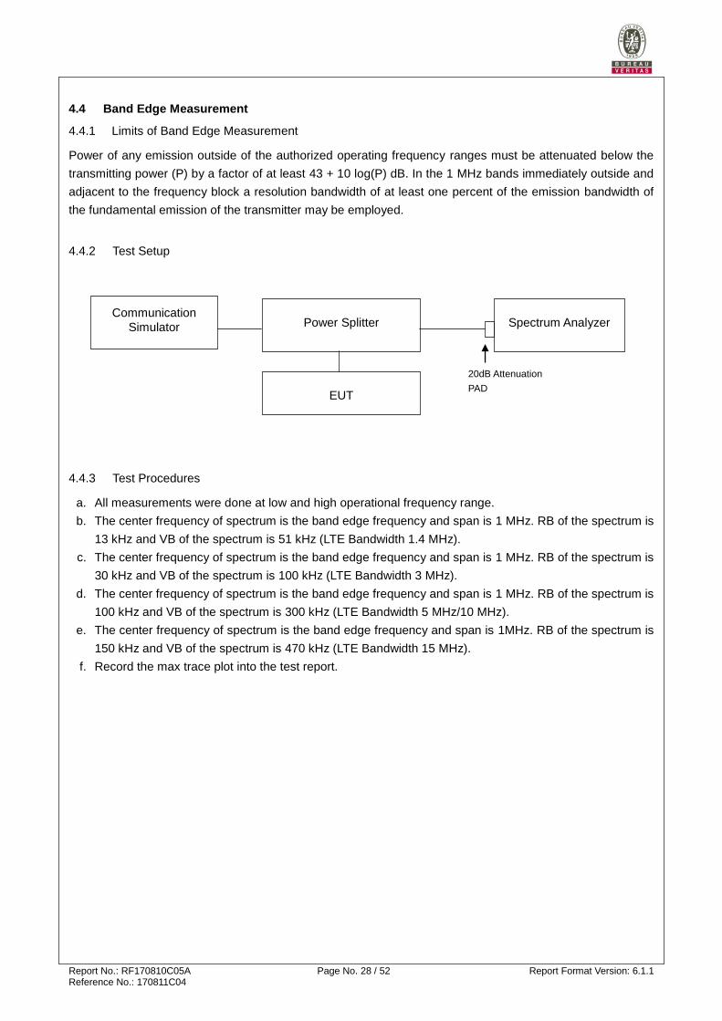
4.4 Band Edge Measurement
4.4.1 Limits of Band Edge Measurement
Power of any emission outside of the authorized operating frequency ranges must be attenuated below the
transmitting power (P) by a factor of at least 43 + 10 log(P) dB. In the 1 MHz bands immediately outside and
adjacent to the frequency block a resolution bandwidth of at least one percent of the emission bandwidth of
the fundamental emission of the transmitter may be employed.
4.4.2 Test Setup
4.4.3 Test Procedures
a. All measurements were done at low and high operational frequency range.
b. The center frequency of spectrum is the band edge frequency and span is 1 MHz. RB of the spectrum is
13 kHz and VB of the spectrum is 51 kHz (LTE Bandwidth 1.4 MHz).
c. The center frequency of spectrum is the band edge frequency and span is 1 MHz. RB of the spectrum is
30 kHz and VB of the spectrum is 100 kHz (LTE Bandwidth 3 MHz).
d. The center frequency of spectrum is the band edge frequency and span is 1 MHz. RB of the spectrum is
100 kHz and VB of the spectrum is 300 kHz (LTE Bandwidth 5 MHz/10 MHz).
e. The center frequency of spectrum is the band edge frequency and span is 1MHz. RB of the spectrum is
150 kHz and VB of the spectrum is 470 kHz (LTE Bandwidth 15 MHz).
f. Record the max trace plot into the test report.
Communication
Simulator Spectrum Analyzer Power Splitter
EUT
20dB Attenuation
PAD
Report No.: RF170810C05A Page No. 29 / 52 Report Format Version: 6.1.1 Reference No.: 170811C04
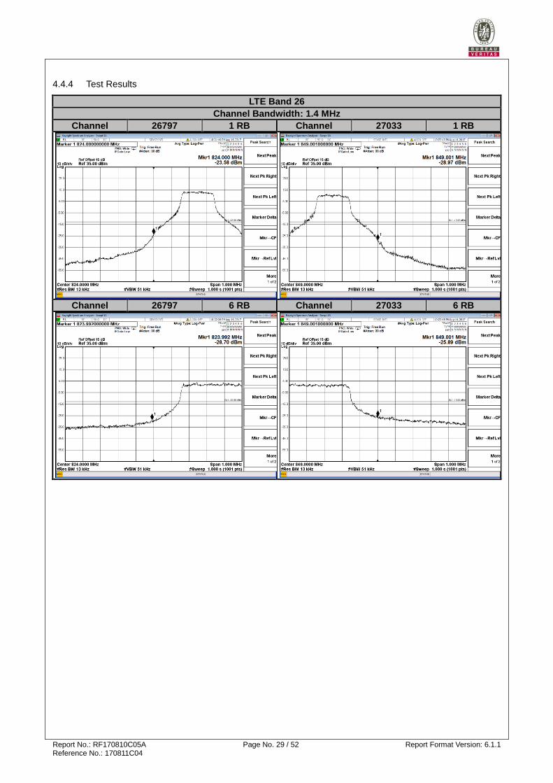
4.4.4 Test Results
LTE Band 26
Channel Bandwidth: 1.4 MHz
Channel 26797 1 RB Channel 27033 1 RB
Channel 26797 6 RB Channel 27033 6 RB

Report No.: RF170810C05A Page No. 30 / 52 Report Format Version: 6.1.1 Reference No.: 170811C04
LTE Band 26
Channel Bandwidth: 3 MHz
Channel 26805 1 RB Channel 27025 1 RB
Channel 26805 15 RB Channel 27025 15 RB

Report No.: RF170810C05A Page No. 31 / 52 Report Format Version: 6.1.1 Reference No.: 170811C04
LTE Band 26
Channel Bandwidth: 5 MHz
Channel 26815 1 RB Channel 27015 1 RB
Channel 26815 25 RB Channel 27015 25 RB
Report No.: RF170810C05A Page No. 32 / 52 Report Format Version: 6.1.1 Reference No.: 170811C04
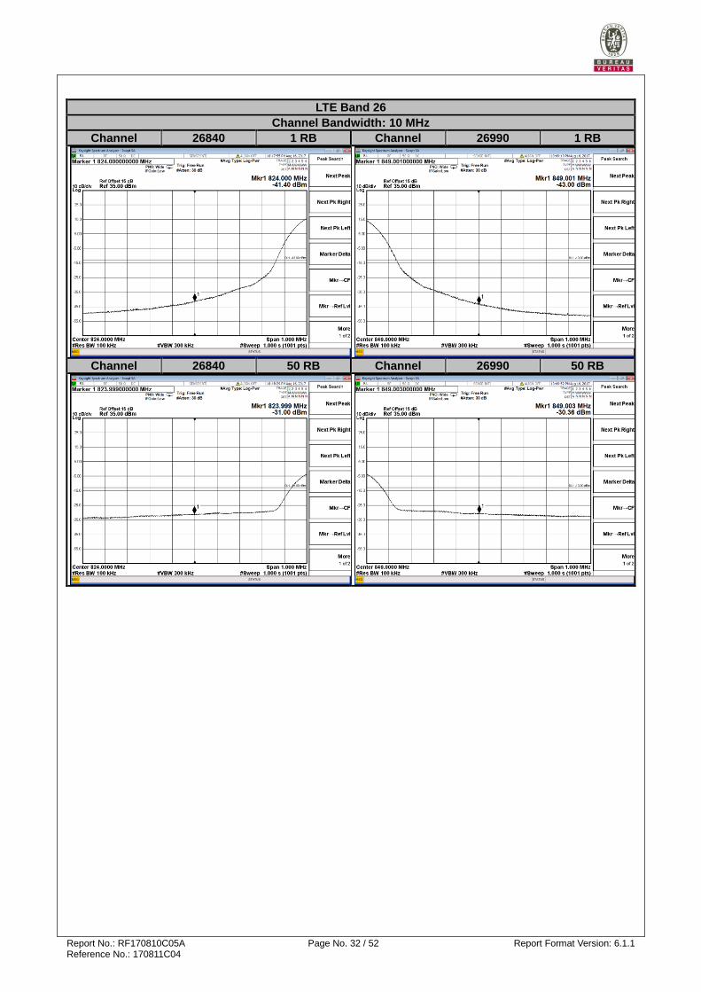
LTE Band 26
Channel Bandwidth: 10 MHz
Channel 26840 1 RB Channel 26990 1 RB
Channel 26840 50 RB Channel 26990 50 RB
Report No.: RF170810C05A Page No. 33 / 52 Report Format Version: 6.1.1 Reference No.: 170811C04
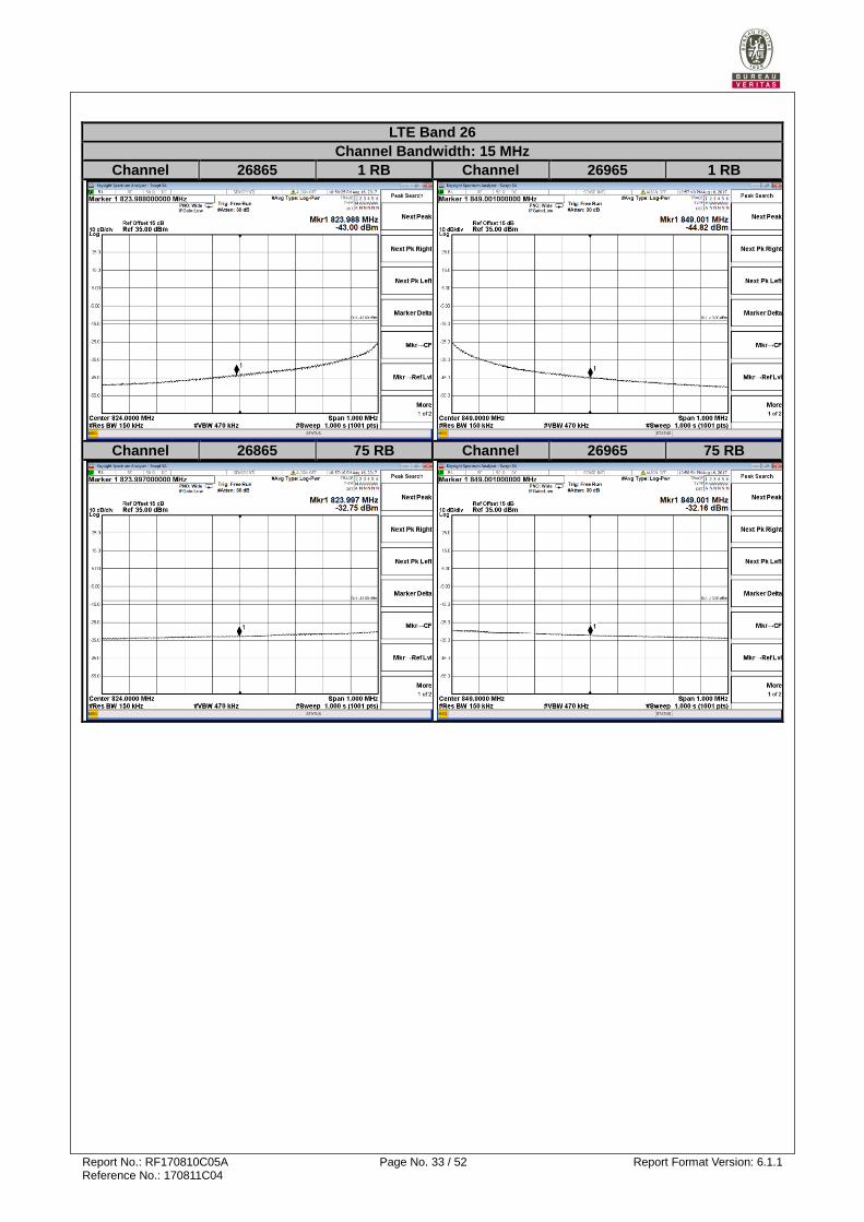
LTE Band 26
Channel Bandwidth: 15 MHz
Channel 26865 1 RB Channel 26965 1 RB
Channel 26865 75 RB Channel 26965 75 RB
Report No.: RF170810C05A Page No. 34 / 52 Report Format Version: 6.1.1 Reference No.: 170811C04
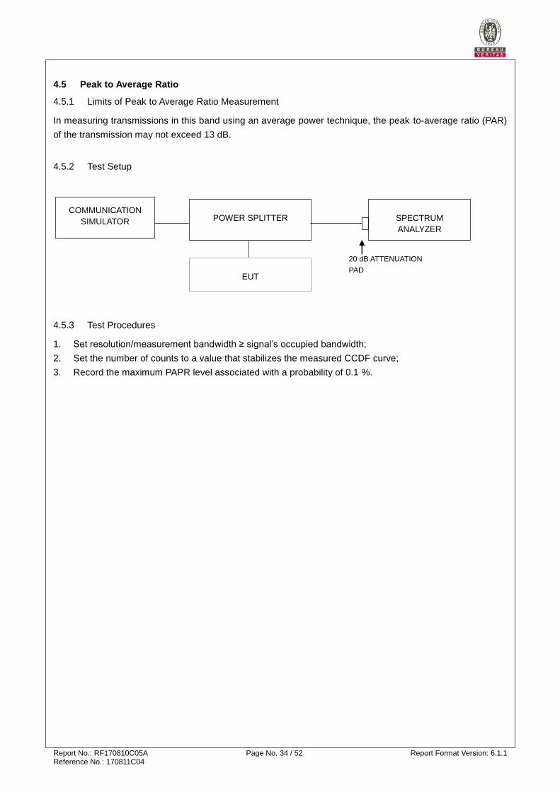
4.5 Peak to Average Ratio
4.5.1 Limits of Peak to Average Ratio Measurement
In measuring transmissions in this band using an average power technique, the peak to-average ratio (PAR)
of the transmission may not exceed 13 dB.
4.5.2 Test Setup
4.5.3 Test Procedures
1. Set resolution/measurement bandwidth ≥ signal’s occupied bandwidth;
2. Set the number of counts to a value that stabilizes the measured CCDF curve;
3. Record the maximum PAPR level associated with a probability of 0.1 %.
COMMUNICATION
SIMULATOR SPECTRUM
ANALYZER
POWER SPLITTER
EUT
20 dB ATTENUATION
PAD
Report No.: RF170810C05A Page No. 35 / 52 Report Format Version: 6.1.1 Reference No.: 170811C04
4.5.4 Test Results
LTE Band 26
Channel Bandwidth: 1.4 MHz Channel Bandwidth: 3 MHz
Channel Frequency
(MHz)
Peak to Average Ratio
(dB) Channel Frequency
(MHz)
Peak to Average Ratio
(dB)
QPSK 16QAM QPSK 16QAM
26797 824.7 3.65 4.51 26805 825.5 3.62 4.62
26915 836.5 3.65 4.48 26915 836.5 3.59 4.46
27033 848.3 2.96 3.89 27025 847.5 3.16 4.24
Spectrum Plot of Worst Value
1.4 MHz / QPSK 1.4 MHz / 16QAM
3 MHz / QPSK 3 MHz / 16QAM
Report No.: RF170810C05A Page No. 36 / 52 Report Format Version: 6.1.1 Reference No.: 170811C04
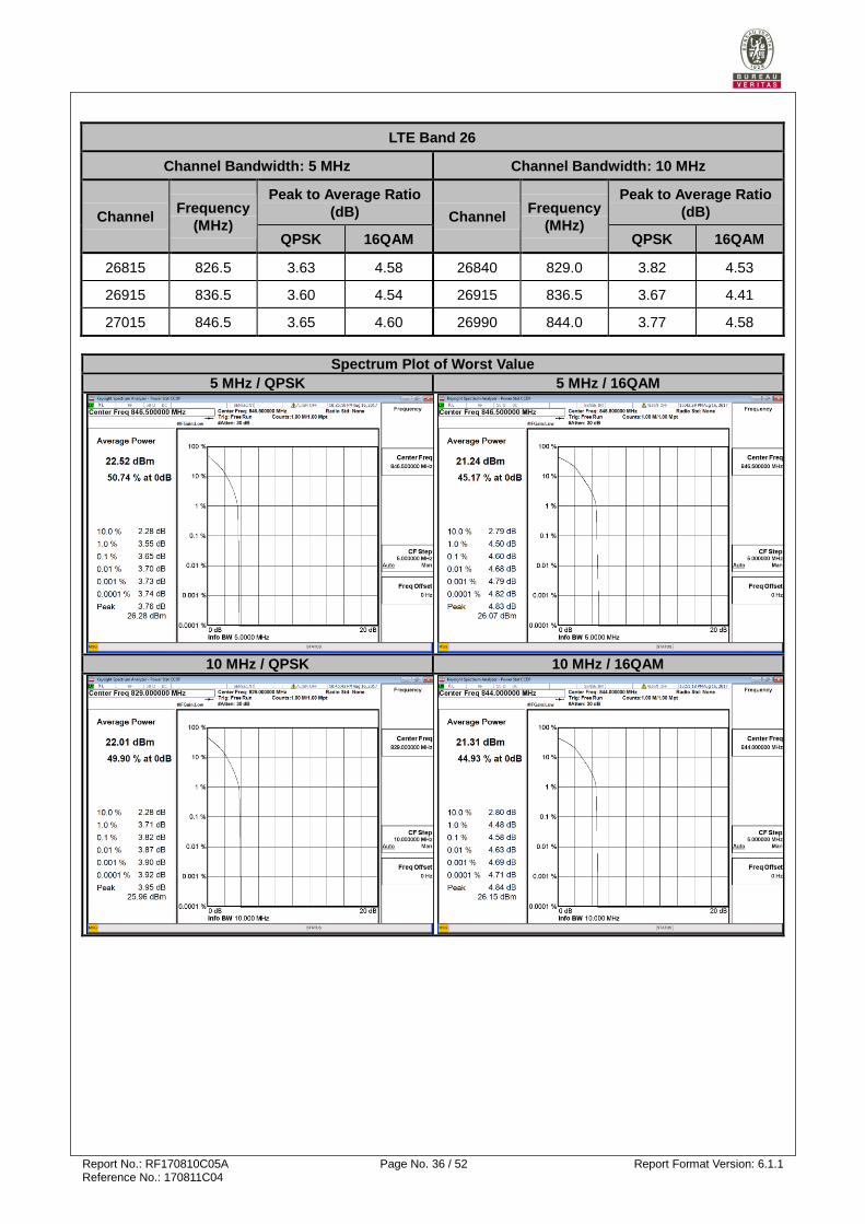
LTE Band 26
Channel Bandwidth: 5 MHz Channel Bandwidth: 10 MHz
Channel Frequency
(MHz)
Peak to Average Ratio
(dB) Channel Frequency
(MHz)
Peak to Average Ratio
(dB)
QPSK 16QAM QPSK 16QAM
26815 826.5 3.63 4.58 26840 829.0 3.82 4.53
26915 836.5 3.60 4.54 26915 836.5 3.67 4.41
27015 846.5 3.65 4.60 26990 844.0 3.77 4.58
Spectrum Plot of Worst Value
5 MHz / QPSK 5 MHz / 16QAM
10 MHz / QPSK 10 MHz / 16QAM
Report No.: RF170810C05A Page No. 37 / 52 Report Format Version: 6.1.1 Reference No.: 170811C04
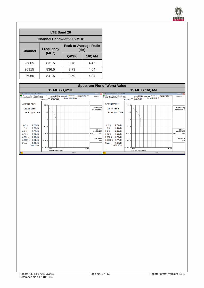
LTE Band 26
Channel Bandwidth: 15 MHz
Channel Frequency
(MHz)
Peak to Average Ratio
(dB)
QPSK 16QAM
26865 831.5 3.78 4.46
26915 836.5 3.73 4.64
26965 841.5 3.59 4.34
Spectrum Plot of Worst Value
15 MHz / QPSK 15 MHz / 16QAM
Report No.: RF170810C05A Page No. 38 / 52 Report Format Version: 6.1.1 Reference No.: 170811C04
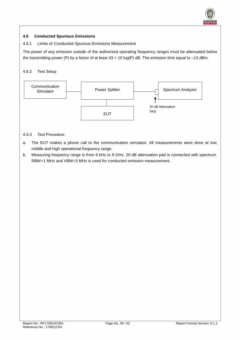
4.6 Conducted Spurious Emissions
4.6.1 Limits of Conducted Spurious Emissions Measurement
The power of any emission outside of the authorized operating frequency ranges must be attenuated below
the transmitting power (P) by a factor of at least 43 + 10 log(P) dB. The emission limit equal to –13 dBm.
4.6.2 Test Setup
4.6.3 Test Procedure
a. The EUT makes a phone call to the communication simulator. All measurements were done at low,
middle and high operational frequency range.
b. Measuring frequency range is from 9 kHz to 9 GHz. 20 dB attenuation pad is connected with spectrum.
RBW=1 MHz and VBW=3 MHz is used for conducted emission measurement.
Communication
Simulator Spectrum Analyzer Power Splitter
EUT
20 dB Attenuation
PAD
Report No.: RF170810C05A Page No. 39 / 52 Report Format Version: 6.1.1 Reference No.: 170811C04
4.6.4 Test Results
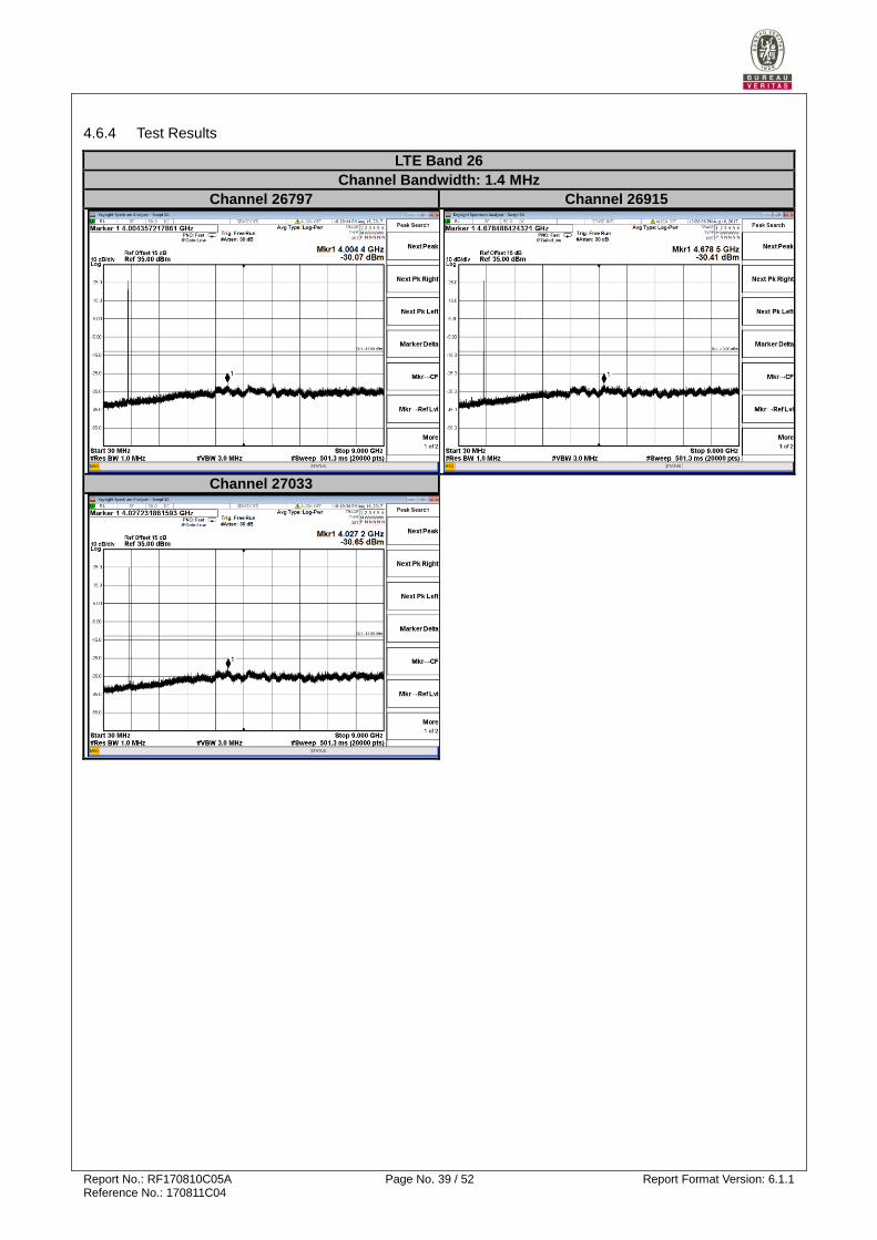
LTE Band 26
Channel Bandwidth: 1.4 MHz
Channel 26797 Channel 26915
Channel 27033
Report No.: RF170810C05A Page No. 40 / 52 Report Format Version: 6.1.1 Reference No.: 170811C04
LTE Band 26
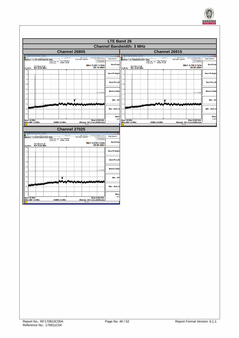
Channel Bandwidth: 3 MHz
Channel 26805 Channel 26915
Channel 27025
Report No.: RF170810C05A Page No. 41 / 52 Report Format Version: 6.1.1 Reference No.: 170811C04
LTE Band 26
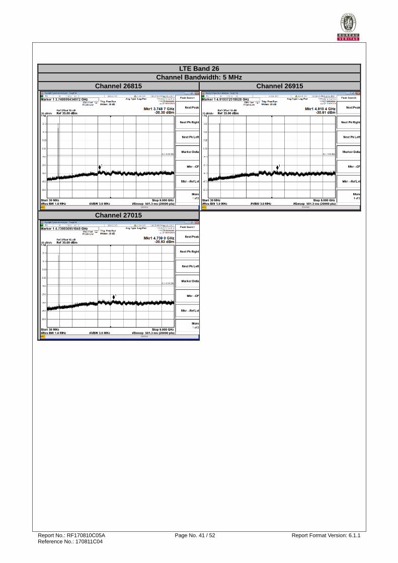
Channel Bandwidth: 5 MHz
Channel 26815 Channel 26915
Channel 27015

Report No.: RF170810C05A Page No. 42 / 52 Report Format Version: 6.1.1 Reference No.: 170811C04
LTE Band 26
Channel Bandwidth: 10 MHz
Channel 26840 Channel 26915
Channel 26990
Report No.: RF170810C05A Page No. 43 / 52 Report Format Version: 6.1.1 Reference No.: 170811C04
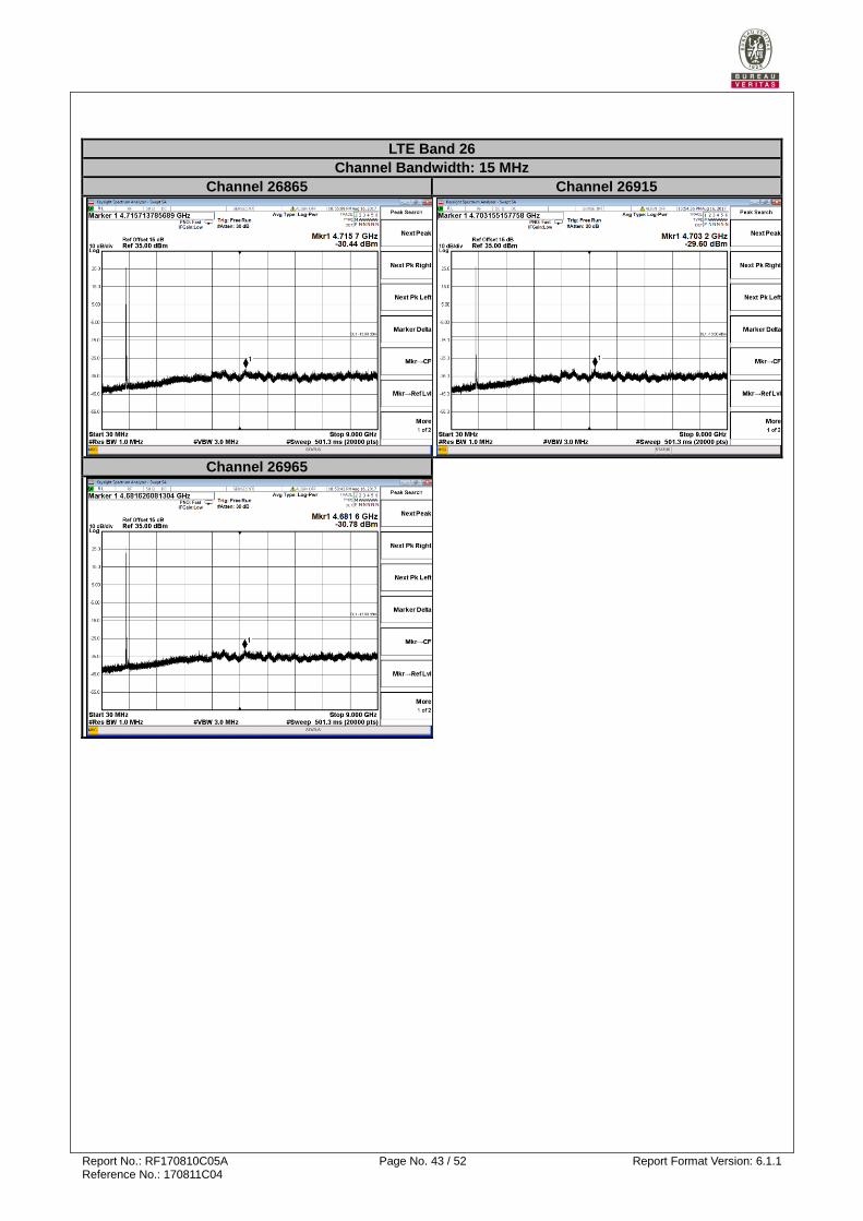
LTE Band 26
Channel Bandwidth: 15 MHz
Channel 26865 Channel 26915
Channel 26965
Report No.: RF170810C05A Page No. 44 / 52 Report Format Version: 6.1.1 Reference No.: 170811C04
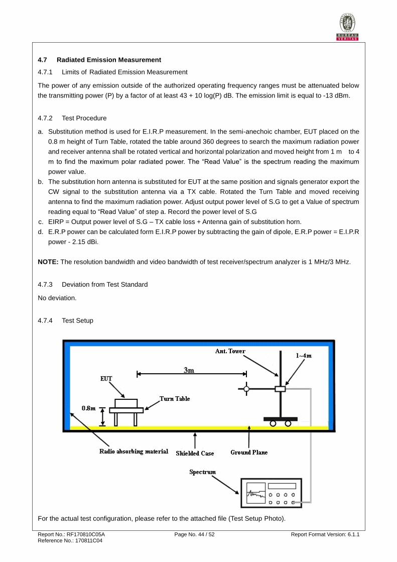
4.7 Radiated Emission Measurement
4.7.1 Limits of Radiated Emission Measurement
The power of any emission outside of the authorized operating frequency ranges must be attenuated below
the transmitting power (P) by a factor of at least 43 + 10 log(P) dB. The emission limit is equal to -13 dBm.
4.7.2 Test Procedure
a. Substitution method is used for E.I.R.P measurement. In the semi-anechoic chamber, EUT placed on the
0.8 m height of Turn Table, rotated the table around 360 degrees to search the maximum radiation power
and receiver antenna shall be rotated vertical and horizontal polarization and moved height from 1 m to 4
m to find the maximum polar radiated power. The “Read Value” is the spectrum reading the maximum
power value.
b. The substitution horn antenna is substituted for EUT at the same position and signals generator export the
CW signal to the substitution antenna via a TX cable. Rotated the Turn Table and moved receiving
antenna to find the maximum radiation power. Adjust output power level of S.G to get a Value of spectrum
reading equal to “Read Value” of step a. Record the power level of S.G
c. EIRP = Output power level of S.G – TX cable loss + Antenna gain of substitution horn.
d. E.R.P power can be calculated form E.I.R.P power by subtracting the gain of dipole, E.R.P power = E.I.P.R
power - 2.15 dBi.
NOTE: The resolution bandwidth and video bandwidth of test receiver/spectrum analyzer is 1 MHz/3 MHz.
4.7.3 Deviation from Test Standard
No deviation.
4.7.4 Test Setup
For the actual test configuration, please refer to the attached file (Test Setup Photo).
Report No.: RF170810C05A Page No. 45 / 52 Report Format Version: 6.1.1 Reference No.: 170811C04
4.7.5 Test Results
LTE Band 26
Channel Bandwidth: 15 MHz / QPSK
Low Channel
Report No.: RF170810C05A Page No. 46 / 52 Report Format Version: 6.1.1 Reference No.: 170811C04
Frequency (MHz)
ERP(dBm) Limit(dBm) Over Limit
(dB)
SPA. Reading (dBm)
S.G. Power (dBm)
TX Cable loss (dB)
TX Antenna
Gain (dBi)
Polarization (H/V)
Result
2494.5 -50.58 -13 -37.58 -59.35 -50.01 4.57 6.15 H Pass
2494.5 -53.28 -13 -40.28 -62.14 -52.71 4.57 6.15 V Pass
Report No.: RF170810C05A Page No. 47 / 52 Report Format Version: 6.1.1 Reference No.: 170811C04
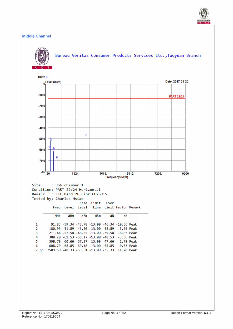
Middle Channel
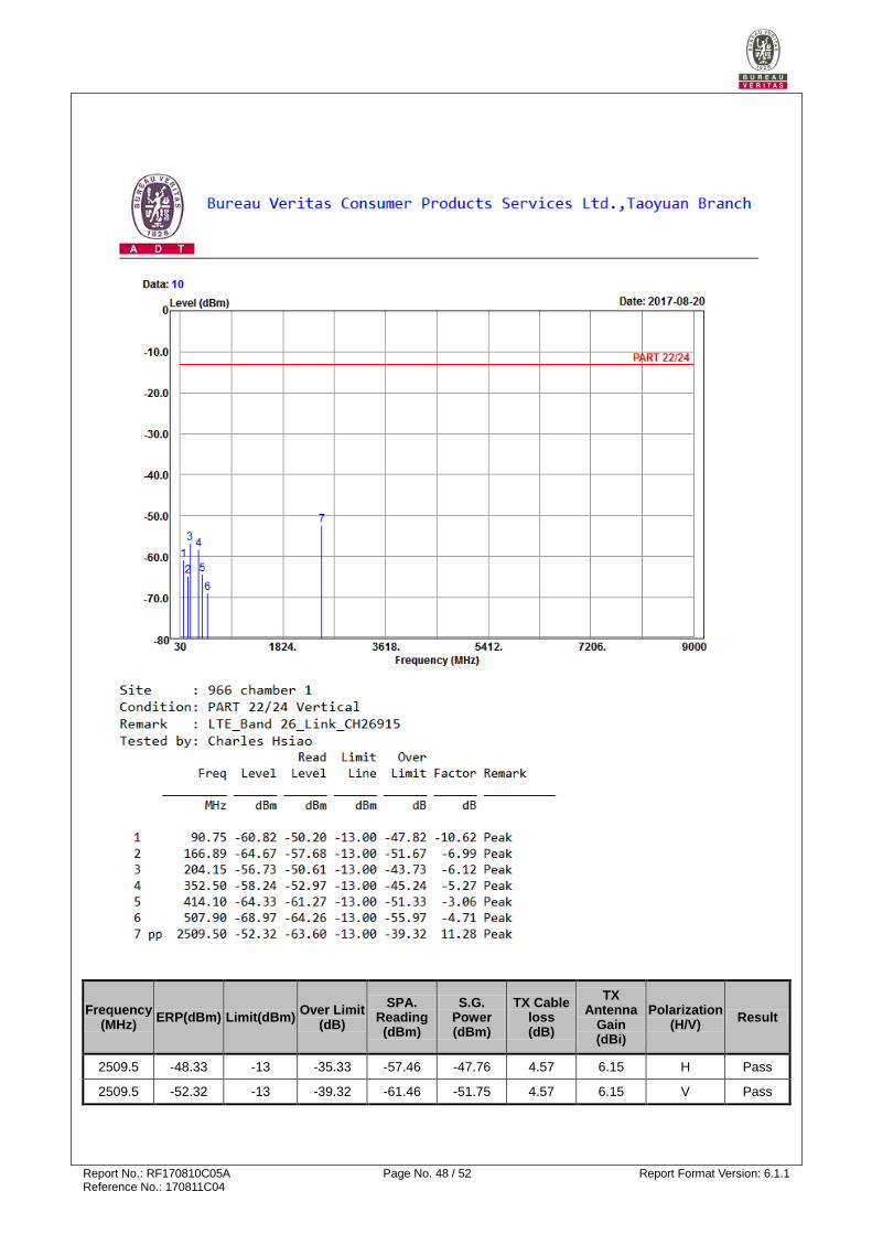
Report No.: RF170810C05A Page No. 48 / 52 Report Format Version: 6.1.1 Reference No.: 170811C04
Frequency (MHz)
ERP(dBm) Limit(dBm) Over Limit
(dB)
SPA. Reading (dBm)
S.G. Power (dBm)
TX Cable loss (dB)
TX Antenna
Gain (dBi)
Polarization (H/V)
Result
2509.5 -48.33 -13 -35.33 -57.46 -47.76 4.57 6.15 H Pass
2509.5 -52.32 -13 -39.32 -61.46 -51.75 4.57 6.15 V Pass
Report No.: RF170810C05A Page No. 49 / 52 Report Format Version: 6.1.1 Reference No.: 170811C04
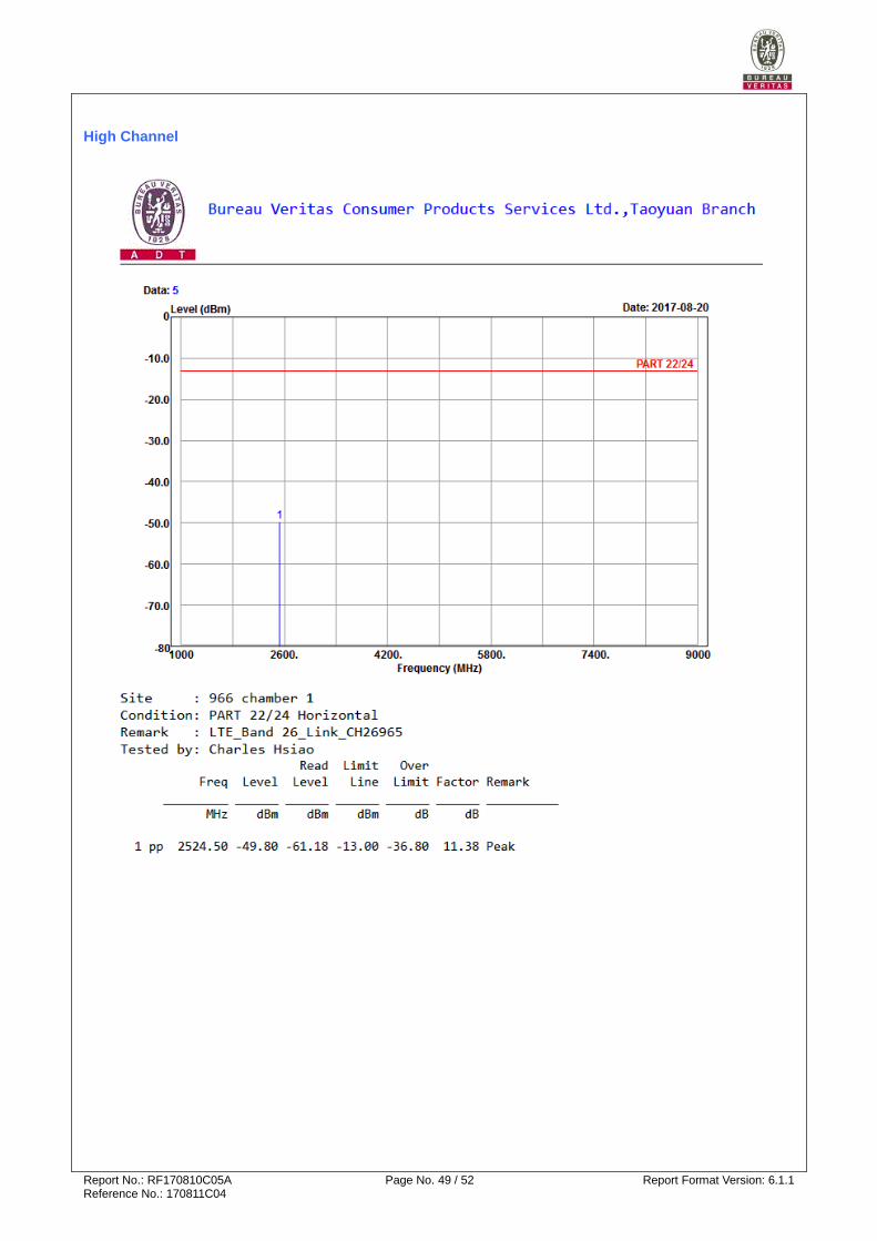
High Channel
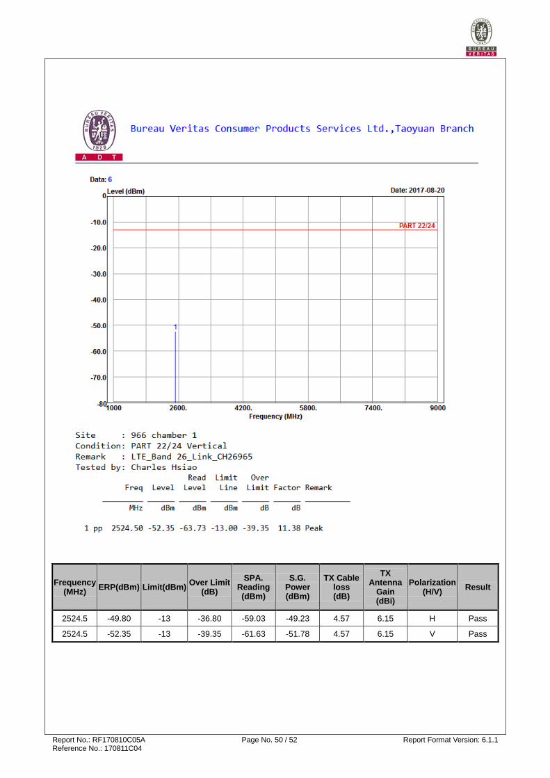
Report No.: RF170810C05A Page No. 50 / 52 Report Format Version: 6.1.1 Reference No.: 170811C04
Frequency (MHz)
ERP(dBm) Limit(dBm) Over Limit
(dB)
SPA. Reading (dBm)
S.G. Power (dBm)
TX Cable loss (dB)
TX Antenna
Gain (dBi)
Polarization (H/V)
Result
2524.5 -49.80 -13 -36.80 -59.03 -49.23 4.57 6.15 H Pass
2524.5 -52.35 -13 -39.35 -61.63 -51.78 4.57 6.15 V Pass
Report No.: RF170810C05A Page No. 51 / 52 Report Format Version: 6.1.1 Reference No.: 170811C04
5 Pictures of Test Arrangements
Please refer to the attached file (Test Setup Photo).
Report No.: RF170810C05A Page No. 52 / 52 Report Format Version: 6.1.1 Reference No.: 170811C04
Appendix – Information on the Testing Laboratories
We, Bureau Veritas Consumer Products Services (H.K.) Ltd., Taoyuan Branch, were founded in 1988 to
provide our best service in EMC, Radio, Telecom and Safety consultation. Our laboratories are FCC
recognized accredited test firms and accredited according to ISO/IEC 17025.
If you have any comments, please feel free to contact us at the following:
Linko EMC/RF Lab
Tel: 886-2-26052180
Fax: 886-2-26051924
Hsin Chu EMC/RF/Telecom Lab
Tel: 886-3-6668565
Fax: 886-3-6668323
Hwa Ya EMC/RF/Safety
Tel: 886-3-3183232
Fax: 886-3-3270892
Email: [email protected]
Web Site: www.bureauveritas-adt.com
The address and road map of all our labs can be found in our web site also.
--- END ---


