FAN7385 Dual-Channel High-Side Gate-Drive ICdocs-europe.electrocomponents.com/webdocs/12cf/... ·...
15
© 2006 Fairchild Semiconductor Corporation www.fairchildsemi.com FAN7385 Dual-Channel High-Side Gate-Drive IC February 2007 FAN7385 Rev. 1.0.2 FAN7385 Dual-Channel High-Side Gate-Drive IC Features Floating Channel for Bootstrap Operation to +600V Typically 350mA/650mA Sourcing/Sinking Current Driving Capability Extended Allowable Negative V S Swing to -9.8V for Signal Propagation at V DD =V BS =15V High-Side Output In-Phase of Input Signal V DD & V BS Supply Range from 10V to 20V 3.3V and 5V Input Logic Compatible Built-in Common Mode dv/dt Noise Canceling Circuit Built-in UVLO Functions for Both Channels Applications Normal Half-Bridge and Full-Bridge Driver PDP Energy Recovery Switch Control Driver Switching Mode Power Supply Description The FAN7385 is a monolithic high side gate drive IC designed for high voltage, high speed driving MOSFETs and IGBTs operating up to +600V. Fairchild’s high-voltage process and common-mode noise canceling technique provide stable operation of high-side drivers under high-dv/dt noise circumstances. An advanced level-shift circuit allows high-side gate driver operation up to V S = -9.8V (typical) for V BS = 15V. The UVLO circuits prevent malfunction when V BS1 and V BS2 are lower than the specified threshold voltage. Output drivers typically source/sink 350mA/650mA, respectively, which is suitable for dual high-side switches and half-bridge inverters. Ordering Information Note: 1. These devices passed wave soldering test by JESD22A-111. 14-SOP Part Number Package Pb-Free Operating Temperature Range Packing Method FAN7385M (1) 14-SOP Yes -40°C ~ 125°C Tube FAN7385MX (1) Tape & Reel
Transcript of FAN7385 Dual-Channel High-Side Gate-Drive ICdocs-europe.electrocomponents.com/webdocs/12cf/... ·...

© 2006 Fairchild Semiconductor Corporation www.fairchildsemi.com
FAN
7385 Dual-C
hannel High-Side G
ate-Drive IC
February 2007
FAN7385 Rev. 1.0.2
FAN7385Dual-Channel High-Side Gate-Drive ICFeatures
Floating Channel for Bootstrap Operation to +600VTypically 350mA/650mA Sourcing/Sinking Current Driving Capability Extended Allowable Negative VS Swing to -9.8V for Signal Propagation at VDD=VBS=15VHigh-Side Output In-Phase of Input SignalVDD & VBS Supply Range from 10V to 20V 3.3V and 5V Input Logic CompatibleBuilt-in Common Mode dv/dt Noise Canceling CircuitBuilt-in UVLO Functions for Both Channels
ApplicationsNormal Half-Bridge and Full-Bridge DriverPDP Energy Recovery Switch Control DriverSwitching Mode Power Supply
Description The FAN7385 is a monolithic high side gate drive ICdesigned for high voltage, high speed driving MOSFETsand IGBTs operating up to +600V.
Fairchild’s high-voltage process and common-modenoise canceling technique provide stable operation ofhigh-side drivers under high-dv/dt noise circumstances.
An advanced level-shift circuit allows high-side gatedriver operation up to VS = -9.8V (typical) for VBS = 15V.
The UVLO circuits prevent malfunction when VBS1 andVBS2 are lower than the specified threshold voltage.
Output drivers typically source/sink 350mA/650mA,respectively, which is suitable for dual high-side switchesand half-bridge inverters.
Ordering Information
Note:1. These devices passed wave soldering test by JESD22A-111.
1
14-SOP
Part Number Package Pb-FreeOperating Temperature
Range Packing MethodFAN7385M(1)
14-SOP Yes -40°C ~ 125°CTube
FAN7385MX(1) Tape & Reel
FAN
7385 Dual-C
hannel High-Side G
ate-Drive IC
© 2006 Fairchild Semiconductor Corporation www.fairchildsemi.comFAN7385 Rev. 1.0.2 2
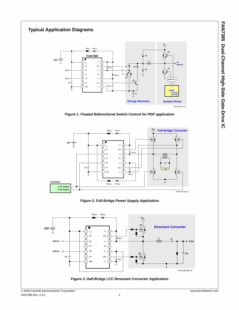
Typical Application Diagrams
Figure 1. Floated Bidirectional Switch Control for PDP application
Figure 2. Full-Bridge Power Supply Application
Figure 3. Half-Bridge LCC Resonant Converter Application
Energy Recovery Sustain Driver
VS
HVICFAN7380FAN7382
DBOOT1
D2
C2
C1
IN1
To Pannel
DBOOT2
CBOOT2
CBOOT1
Q1
Q2
D1
D3
D4
Q3
Q4
L1
IN2
15VFAN7385
Buffer IC
FAN7385 Rev.01
RBOOT
IN1
IN2
GND
NC
HO1
NC
HO2
1
2 NC
5
7
13
11
10
9
12
8
14
3
4
6
NC
VDD
VS1
VB1
VB2
VS2
Full-Bridge ConverterDBOOT1
C1
CBOOT1
15V
VDC
Load
CBOOT2
DBOOT2
L-CH OutputR-CH Output
Controller
IN1
IN2
GND
NC
HO1
NC
HO2
1
2 NC
5
7
13
11
10
9
12
8
14
3
4
6
NC
VDD
VS1
VB1
VB2
VS2
RBOOT1
RBOOT2
FAN7385 Rev.01
Resonant Converter
DBOOT
C1
INPUT1
CBOOT
15V
INPUT2
FAN7385 Rev.01
C2
Q1
Q2
L CVout
Co
IN1
IN2
GND
NC
HO1
NC
HO2
1
2 NC
5
7
13
11
10
9
12
8
14
3
4
6
NC
VDD
VS1
VB1
VB2
VS2
RBOOT
VDC

FAN
7385 Dual-C
hannel High-Side G
ate-Drive IC
© 2006 Fairchild Semiconductor Corporation www.fairchildsemi.comFAN7385 Rev. 1.0.2 3
Internal Block Diagram
Figure 4. Functional Block Diagram
NOISECANCELLER
UVLO
RRS Q
DR
IVERPULSE
GEN
ERA
TOR
NOISECANCELLER
UVLO
RRS Q
DR
IVERPULSE
GEN
ERA
TOR
5
1
10
9
8
14
13
500K
500K
12
IN2
IN1
VDD
GND
VB2
VS2
HO2
VB1
HO1
VS1
Pin 2, 4, 6 and 11 are not connection
SCHMITT TRIGGER INPUT
7
3
FAN7385 Rev.01

FAN
7385 Dual-C
hannel High-Side G
ate-Drive IC
© 2006 Fairchild Semiconductor Corporation www.fairchildsemi.comFAN7385 Rev. 1.0.2 4
Pin Configuration
Figure 5. Pin Configuration (Top View)
Pin DefinitionsPin # Name Description
1 VDD Power supply
2 NC Not connection
3 IN1 Channel 1 control input
4 NC Not connection
5 IN2 Channel 2 control input
6 NC Not connection
7 GND Ground
8 VS2 Channel 2 floating supply return
9 HO2 Channel 2 output
10 VB2 Channel 2 floating supply
11 NC Not connection
12 VS1 Channel 1 floating supply return
13 HO1 Channel 1 output
14 VB1 Channel 1 floating supply
FAN7385
VB1VDD
IN1
IN2
NC
GND
HO1
VS1
NC
VB2
HO2
VS2
NC
NC
FAN7385 Rev.00
14
13
12
11
10
9
8
1
2
3
4
5
6
7

FAN
7385 Dual-C
hannel High-Side G
ate-Drive IC
© 2006 Fairchild Semiconductor Corporation www.fairchildsemi.comFAN7385 Rev. 1.0.2 5
Absolute Maximum RatingsStresses exceeding the absolute maximum ratings may damage the device. The device may not function or be opera-ble above the recommended operating conditions and stressing the parts to these levels is not recommended. In addi-tion, extended exposure to stresses above the recommended operating conditions may affect device reliability. Theabsolute maximum ratings are stress ratings only. TA=25°C, unless otherwise specified.
Notes: 2. Mounted on 76.2 x 114.3 x 1.6mm PCB (FR-4 glass epoxy material).3. Refer to the following standards: JESD51-2: Integral circuits thermal test method environmental conditions - natural convection JESD51-3: Low effective thermal conductivity test board for leaded surface mount packages4. Do not exceed PD under any circumstances.
Recommended Operating ConditionsThe Recommended Operating Conditions table defines the conditions for actual device operation. Recommendedoperating conditions are specified to ensure optimal performance to the datasheet specifications. Fairchild does notrecommend exceeding them or designing to Absolute Maximum Ratings.
Symbol Parameter Min. Max. UnitVS High-side offset voltage VS1 ,VS2 VB-25 VB+0.3 V
VB High-side floating supply voltage VB1 ,VB2 -0.3 625 V
VHO High-side floating output voltage HO1, HO2 VS-0.3 VB+0.3 V
VDD Low-side and logic-fixed supply voltage -0.3 25 V
VIN Logic input voltage (IN1, IN2) -0.3 VDD+0.3 V
GND Logic ground VDD-25 VDD+0.3 V
dVS/dt Allowable offset voltage slew rate 50 V/ns
PD(2)(3)(4) Power dissipation 1.0 W
θJA Thermal resistance, junction-to-ambient 110 °C/W
TJ Junction temperature 150 °C
TS Storage temperature 150 °C
Symbol Parameter Condition Min. Max. UnitVB High-side floating supply voltage VS+10 VS+20 V
VS High-side floating supply offset voltage 6-VDD 600 V
VDD Supply voltage 10 20 V
VHO High-side (HO1, HO2) output voltage VS VB V
VIN Logic input voltage (IN1, IN2) GND VDD V
TA Ambient temperature -40 125 °C

FAN
7385 Dual-C
hannel High-Side G
ate-Drive IC
© 2006 Fairchild Semiconductor Corporation www.fairchildsemi.comFAN7385 Rev. 1.0.2 6
Electrical CharacteristicsVBIAS (VDD, VBS1, VBS2) = 15.0V, TA = 25°C, unless otherwise specified. The VIN and IIN parameters are referenced toGND. The VO and IO parameters are referenced to VS1 and VS2 and are applicable to the respective outputs HO1 andHO2.
Dynamic Electrical CharacteristicsTA=25°C, VBIAS (VDD, VBS1, VBS2) = 15.0V, VS1 = VS2 = GND, CLoad = 1000pF unless otherwise specified.
Notes: 5. This parameter guaranteed by design.
Symbol Characteristics Condition Min. Typ. Max. UnitSUPPLY CURRENT SECTION
IQDD Quiescent VDD supply current VIN1=VIN2=0V or 5V 28 50 μAIPDD Operating VDD supply current fIN1=fIN2=10kHz, rms value 35 70 μA
BOOTSTRAPPED POWER SUPPLY SECTION
VBSUV+VBS1 and VBS2 supply under-voltage positive going threshold VBS1=VBS2=Sweep 8.2 9.1 10.2 V
VBSUV-VBS1 and VBS2 supply under-voltage negative going threshold VBS1=VBS2=Sweep 7.6 8.5 9.6 V
VBSHYSVBS1 and VBS2 supply under-voltage lockout hysteresis VBS1=VBS2=Sweep 0.6 V
ILK Offset supply leakage current VB=VS=600V 10 μAIQBS1,2 Quiescent VBS1 and VBS2 supply current VIN1=0V or 5V 50 85 μAIPBS1,2 Operating VBS1 and VBS2 supply current fIN1=10kHz, rms value 220 300 μA
GATE DRIVER OUTPUT SECTIONVOH High-level output voltage, VBIAS-VO IO=0mA (No Load) 30 mVVOL Low-level output voltage, VO IO=0mA (No Load) 30 mVIO+ Output HIGH short-circuit pulse current VO=0V, VIN=5V with PW<10µs 250 350 mAIO- Output LOW short-circuit pulsed current VO=15V, VIN=0V with PW<10µs 500 650 mA
VSAllowable negative VS pin voltage for IN signal propagation to HO
-9.8 -7.0 V
LOGIC INPUT SECTION (IN1 AND IN2)VIH Logic "1" input voltage 2.5 VVIL Logic "0" input voltage 1.3 VIIN+ Logic "1" input bias current VIN=5V 10 20 μAIIN- Logic "0" input bias current VIN=0V 2.0 μARIN Input pull-down resistance 400 500 600 KΩ
Symbol Parameter Conditions Min. Typ. Max. Unitton Turn-on propagation delay VS=0V 110 180 ns
toff Turn-off propagation delay VS=0V or 600V(5) 110 180 ns
tr Turn-on rise time 50 90 ns
tf Turn-off fall time 30 70 ns
MT Delay matching, Channel 1 & 2 turn-on/off 0 ns

FAN
7385 Dual-C
hannel High-Side G
ate-Drive IC
© 2006 Fairchild Semiconductor Corporation www.fairchildsemi.comFAN7385 Rev. 1.0.2 7
Typical Characteristics
Figure 6. VBS UVLO (+) vs. Temperature Figure 7. VBS UVLO (-) vs. Temperature
Figure 8. VBS UVLO Hysteresis vs. Temperature Figure 9. VDD Quiescent Current vs. Temperature
Figure 10. VBS Quiescent Current vs. Temperature Figure 11. VDD Operating Current vs. Temperature
-40 -20 0 20 40 60 80 100 1208.00
8.25
8.50
8.75
9.00
9.25
9.50
9.75
10.00
V BSU
VP [V
]
Temperature [°C]-40 -20 0 20 40 60 80 100 120
8.0
8.2
8.4
8.6
8.8
9.0
VBS
UVN
[V]
Temperature [°C]
-40 -20 0 20 40 60 80 100 1200.0
0.2
0.4
0.6
0.8
1.0
VBS
HYS
[V]
Temperature [°C]-40 -20 0 20 40 60 80 100 1200
10
20
30
40
50
60
70
I Q
DD [μ
A]
Temperature [°C]
VIN1= VIN2=GND
-40 -20 0 20 40 60 80 100 1200
10
20
30
40
50
60
70
I QBS
[μA
]
Temperature [°C]
VIN1= VIN2=GND
-40 -20 0 20 40 60 80 100 12010
20
30
40
50
60
70
80
I PDD [μ
A]
Temperature [°C]

FAN
7385 Dual-C
hannel High-Side G
ate-Drive IC
© 2006 Fairchild Semiconductor Corporation www.fairchildsemi.comFAN7385 Rev. 1.0.2 8
Typical Characteristics (Continued)
Figure 12. VBS Operating Current vs. Temperature Figure 13. Logic High Input Current vs. Temperature
Figure 14. Logic Low Input Current vs. Temperature Figure 15. Logic Input High Voltage vs. Temperature
Figure 16. Logic Input Low Voltage vs. Temperature Figure 17. Logic Input Resistance vs. Temperature
-40 -20 0 20 40 60 80 100 120100
125
150
175
200
225
250
275
300
I PBS [μ
A]
Temperature [°C]-40 -20 0 20 40 60 80 100 12002468
101214161820
IN+
[μA
]
Temperature [°C]
-40 -20 0 20 40 60 80 100 120-2.0
-1.5
-1.0
-0.5
0.0
0.5
1.0
1.5
2.0
IN- [μA
]
Temperature [°C]-40 -20 0 20 40 60 80 100 120
2.0
2.1
2.2
2.3
2.4
2.5
2.6
2.7
V
IH [V
]
Temperature [°C]
-40 -20 0 20 40 60 80 100 1201.01.11.21.31.41.51.61.71.81.92.0
VIL [V
]
Temperature [°C]-40 -20 0 20 40 60 80 100 1200
200
400
600
800
1000
RIN
[kΩ
]
Temperature [°C]

FAN
7385 Dual-C
hannel High-Side G
ate-Drive IC
© 2006 Fairchild Semiconductor Corporation www.fairchildsemi.comFAN7385 Rev. 1.0.2 9
Typical Characteristics (Continued)
Figure 18. Rising Time vs. Temperature Figure 19. Falling Time vs. Temperature
Figure 20. Turn-On Delay Time vs. Temperature Figure 21. Turn-Off Delay Time vs. Temperature
Figure 22. Delay Matching Time vs. Temperature Figure 23. Allowable Negative VS Voltage for Signal Propagation to High Side vs. Temperature
-40 -20 0 20 40 60 80 100 120102030405060708090
100
t R [n
s]
Temperature [°C]-40 -20 0 20 40 60 80 100 1200
10
20
30
40
50
60
70
80
t F [ns]
Temperature [°C]
-40 -20 0 20 40 60 80 100 12090
100110120130140150160170180
t ON [n
s]
Temperature [°C]-40 -20 0 20 40 60 80 100 120
100
110
120
130
140
150
160
170
180
t O
FF [n
s]
Temperature [°C]
-40 -20 0 20 40 60 80 100 120-15
-10
-5
0
5
10
15
20
MT
[ns]
Temperature [°C]-40 -20 0 20 40 60 80 100 120
-6
-8
-10
-12
-14
VS [V
]
Temperature [°C]

FAN
7385 Dual-C
hannel High-Side G
ate-Drive IC
© 2006 Fairchild Semiconductor Corporation www.fairchildsemi.comFAN7385 Rev. 1.0.2 10
Typical Characteristics (Continued)
Figure 24. Output High Short-Circuit Pulse Current vs. Temperature
Figure 25. Output Low Short-Circuit Pulse Current vs. Temperature
Figure 26. VDD Quiescent Current vs. Supply Voltage
Figure 27. VDD Operating Current vs. Supply Voltage
Figure 28. VBS Operating Current vs. Supply Voltage Figure 29. Rising Time vs. Supply Voltage
-40 -20 0 20 40 60 80 100 120300
320
340
360
380
400
I O+
[V]
Temperature [°C]-40 -20 0 20 40 60 80 100 120
500
550
600
650
700
750
I O- [
V]
Temperature [°C]
0 5 10 15 20 250
20
40
60
80
I QD
D [μ
A]
Supply Voltage [V]0 5 10 15 20
0
20
40
60
80
I PD
D [μ
A]
Supply Voltage [V]
0 5 10 15 200
50
100
150
200
250
I PBS [μ
A]
Supply Voltage [V]10 11 12 13 14 15 16 17 18 19 20
10
20
30
40
50
60
70
80
t R [n
s]
Supply Voltage [V]

FAN
7385 Dual-C
hannel High-Side G
ate-Drive IC
© 2006 Fairchild Semiconductor Corporation www.fairchildsemi.comFAN7385 Rev. 1.0.2 11
Typical Characteristics (Continued)
Figure 30. Falling Time vs. Supply Voltage Figure 31. Turn-On Delay Time vs. Supply Voltage
Figure 32. Turn-Off Delay Time vs. Supply Voltage Figure 33. Output Source Current vs. Supply Voltage
Figure 34. Output Sink Current vs. Supply Voltage Figure 35. Allowable Negative VS Voltage for Signal Propagation to High Side vs. Supply Voltage
10 11 12 13 14 15 16 17 18 19 2010
20
30
40
50
t F [ns]
Supply Voltage [V]10 11 12 13 14 15 16 17 18 19 20
80
90
100
110
120
130
140
150
160
t ON [n
s]
Supply Voltage [V]
10 11 12 13 14 15 16 17 18 19 2080
90
100
110
120
130
140
150
160
t OFF
[ns]
Supply Voltage [V]10 11 12 13 14 15 16 17 18 19 20
200
250
300
350
400
450
500
O
utpu
t Sou
rcin
g C
urre
nt [m
A]
Supply Voltage [V]
10 11 12 13 14 15 16 17 18 19 20400
500
600
700
800
900
1000
Out
put S
ourc
ing
Cur
rent
[mA
]
Supply Voltage [V]10 11 12 13 14 15 16 17 18 19 20
-16
-14
-12
-10
-8
-6
-4
VS
[V]
Supply Voltage [V]

FAN
7385 Dual-C
hannel High-Side G
ate-Drive IC
© 2006 Fairchild Semiconductor Corporation www.fairchildsemi.comFAN7385 Rev. 1.0.2 12
Switching Time Definitions
Figure 36. Switching Time Test Circuit
Figure 37. Input / Output Waveforms
(B)(A)
10μF 0.1μFVDD
15V
HVIC
GND
IN
VB
VS
HO
10μF 0.1μF
IN 15V
1000pF
IN
OUT
50%
90%
50%
ton
10%
tr toff tf
10%
90%
FAN7385 Rev.00
IN1
IN2
HO1
HO2
FAN7385 Rev.00

FAN
7385 Dual-C
hannel High-Side G
ate-Drive IC
© 2006 Fairchild Semiconductor Corporation www.fairchildsemi.comFAN7385 Rev. 1.0.2 13
Typical Application Information1. Under-Voltage Lockout (UVLO)The FAN7385 has an under-voltage lockout (UVLO)protection circuit to prevent malfunction when VBS1 andVBS2 are lower than the specified threshold voltage. TheUVLO circuit monitors the bootstrap capacitor voltages(VBS1, VBS2) independently.
2. Layout ConsiderationFor optimum performance, considerations must be givenduring printed circuit board (PCB) layout.
2.1 Supply Capacitors
If the output stages are able to quickly turn on a switch-ing device with a high current value, the supply capaci-tors must be placed as close as possible to the devicepins (VDD and GND for the ground-tied supply, VB andVS for the floating supply) to minimize parasitic induc-tance and resistance.
2.2 Gate Drive Loop
Current loops behave like antennae, able to receive andtransmit noise. To reduce the noise coupling/emissionand improve the power switch turn-on and off perfor-mances, gate drive loops must be reduced as much aspossible.
2.3 Ground Plane
To minimize noise coupling, avoid placing the groundplane under or near the high-voltage floating side.

FAN
7385 Dual-C
hannel High-Side G
ate-Drive IC
© 2006 Fairchild Semiconductor Corporation www.fairchildsemi.comFAN7385 Rev. 1.0.2 14
Package Dimensions14-SOPDimensions are in millimeters unless otherwise noted.
Figure 38. 14-Lead Small Outline Package (SOP)
January 2001, Rev. A
14sop225b_dim.pdf
8.56
±0.2
0
0.33
7±0
.008
1.27
0.05
0
5.720.225
1.55 ±0.10
0.061 ±0.004
0.050.002
6.00 ±0.30
0.236 ±0.012
3.95 ±0.20
0.156 ±0.008
0.60 ±0.20
0.024 ±0.008
8.70
0.34
3M
AX
#1
#7 #8
0~8°
#14
0.47
0.01
9(
)
1.800.071
MA
X0.
10M
AX
0.00
4
MAX
MIN
+0.
10-0
.05
0.20
+0.
004
-0.0
020.
008
+0.
10-0
.05
0.40
6
+0.
004
-0.0
020.
016

TRADEMARKS
The following are registered and unregistered trademarks Fairchild Semiconductor owns or is authorized to use and is not intended to be an exhaustive list of all such trademarks.
ACEx®
Across the board. Around the world.
ActiveArray
Bottomless
Build it Now
CoolFET
CROSSVOLTCTL™Current Transfer Logic™
DOME
E2CMOS
EcoSPARK®
EnSignaFACT Quiet Series™ FACT
®
FAST®
FASTr
FPSFRFET
®
GlobalOptoisolator
GTO
HiSeC
i-LoImpliedDisconnect
IntelliMAX
ISOPLANAR
MICROCOUPLER
MicroPak
MICROWIRE
MSX
MSXPro
OCX
OCXProOPTOLOGIC
®
OPTOPLANAR®
PACMAN
POPPower220
®
Power247®
PowerEdge
PowerSaver
PowerTrench®
Programmable Active DroopQFET
®
QS
QT Optoelectronics
Quiet Series
RapidConfigure
RapidConnect
ScalarPump
SMART STARTSPM
®
SuperFET
SuperSOT -3
SuperSOT -6
SuperSOT -8
TCMThe Power Franchise
®
™
TinyBoost
TinyBuck
TinyLogic®
TINYOPTO
TinyPower
TinyWire
TruTranslation
SerDesUHC
®
UniFET
VCX
Wire
DISCLAIMER
FAIRCHILD SEMICONDUCTOR RESERVES THE RIGHT TO MAKE CHANGES WITHOUT FURTHER NOTICE TO ANY PRODUCTS HEREIN TO IMPROVE RELIABILITY, FUNCTION OR DESIGN. FAIRCHILD DOES NOT ASSUME ANY LIABILITY ARISING OUT OF THE APPLICATION OR USE OF ANY PRODUCT OR CIRCUIT DESCRIBED HEREIN; NEITHER DOES IT CONVEY ANY LICENSE UNDER ITS PATENT RIGHTS, NOR THE RIGHTS OF OTHERS. THESE SPECIFICATIONS DO NOT EXPAND THE TERMS OF FAIRCHILD’S WORLDWIDE TERMS AND CONDITIONS, SPECIFICALLY THE WARRANTY THEREIN, WHICH COVERS THESE PRODUCTS.
LIFE SUPPORT POLICY
FAIRCHILD’S PRODUCTS ARE NOT AUTHORIZED FOR USE AS CRITICAL COMPONENTS IN LIFE SUPPORT DEVICES OR SYSTEMS WITHOUT THE EXPRESS WRITTEN APPROVAL OF FAIRCHILD SEMICONDUCTOR CORPORATION.
As used herein:
1. Life support devices or systems are devices or systems which, (a) are intended for surgical implant into the body or (b) support or sustain life, and (c) whose failure to perform when properly used in accordance with instructions for use provided in the labeling, can be reasonably expected to result in a significant injury of the user.
2. A critical component in any component of a life support, device, or system whose failure to perform can be reasonably expected to cause the failure of the life support device or system, or to affect its safety or effectiveness.
PRODUCT STATUS DEFINITIONS
Definition of Terms
Datasheet Identification Product Status Definition
Advance Information Formative or In Design This datasheet contains the design specifications for product development. Specifications may change in any manner without notice.
Preliminary First Production This datasheet contains preliminary data; supplementary data will be published at a later date. Fairchild Semiconductor reserves the right to make changes at any time without notice to improve design.
No Identification Needed Full Production This datasheet contains final specifications. Fairchild Semiconductor reserves the right to make changes at any time without notice to improve design.
Obsolete Not In Production This datasheet contains specifications on a product that has been discontinued by Fairchild Semiconductor. The datasheet is printed for reference information only.
Rev. I23
FAN
7385 Dual-C
hannel High-Side G
ate-Drive IC
© 2006 Fairchild Semiconductor Corporation www.fairchildsemi.comFAN7385 Rev. 1.0.2 15
![Index [docs-europe.electrocomponents.com]docs-europe.electrocomponents.com/webdocs/134b/0900766b8134bb17.pdfIndex by product group Technical Info ... S1-M2-02 + Single trigger + 2](https://static.fdocuments.us/doc/165x107/5adcde717f8b9a1a088c933f/index-docs-docs-by-product-group-technical-info-s1-m2-02-single-trigger.jpg)


![Untitled Document [docs-europe.electrocomponents.com]docs-europe.electrocomponents.com/webdocs/0920/0900766b809201d… · Schneider Electric Brands ZELIO-CONTROL Measurement Relays](https://static.fdocuments.us/doc/165x107/5abeae277f8b9a5d718d478e/untitled-document-docs-docs-schneider-electric-brands-zelio-control-measurement.jpg)