


FAMILY OF WIDE-BANDWIDTHHIGH-OUTPUT ... OF WIDE-BANDWIDTHHIGH-OUTPUT-DRIVESINGLE SUPPLY OPERATIONAL...
52
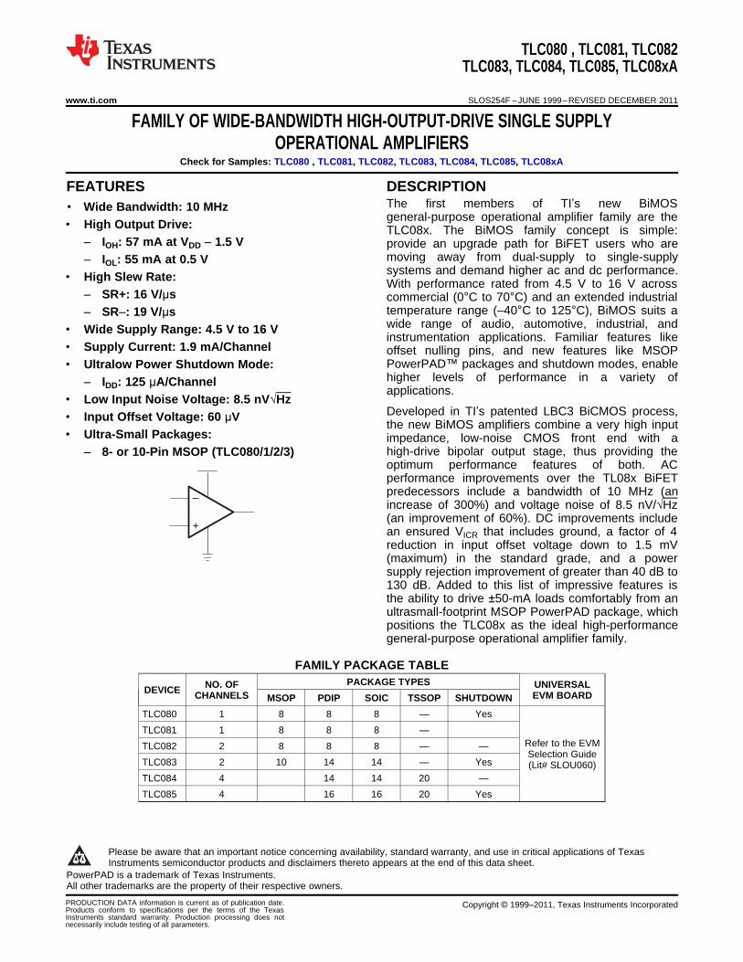
+ – TLC080 , TLC081, TLC082 TLC083, TLC084, TLC085, TLC08xA www.ti.com SLOS254F – JUNE 1999 – REVISED DECEMBER 2011 FAMILY OF WIDE-BANDWIDTH HIGH-OUTPUT-DRIVE SINGLE SUPPLY OPERATIONAL AMPLIFIERS Check for Samples: TLC080 , TLC081, TLC082, TLC083, TLC084, TLC085, TLC08xA 1FEATURES DESCRIPTION The first members of TI’s new BiMOS 23• Wide Bandwidth: 10 MHz general-purpose operational amplifier family are the • High Output Drive: TLC08x. The BiMOS family concept is simple: – I OH : 57 mA at V DD – 1.5 V provide an upgrade path for BiFET users who are moving away from dual-supply to single-supply – I OL : 55 mA at 0.5 V systems and demand higher ac and dc performance. • High Slew Rate: With performance rated from 4.5 V to 16 V across – SR+: 16 V/µs commercial (0°C to 70°C) and an extended industrial temperature range (–40°C to 125°C), BiMOS suits a – SR–: 19 V/µs wide range of audio, automotive, industrial, and • Wide Supply Range: 4.5 V to 16 V instrumentation applications. Familiar features like • Supply Current: 1.9 mA/Channel offset nulling pins, and new features like MSOP PowerPAD™ packages and shutdown modes, enable • Ultralow Power Shutdown Mode: higher levels of performance in a variety of – I DD : 125 µA/Channel applications. • Low Input Noise Voltage: 8.5 nV√Hz Developed in TI’s patented LBC3 BiCMOS process, • Input Offset Voltage: 60 µV the new BiMOS amplifiers combine a very high input • Ultra-Small Packages: impedance, low-noise CMOS front end with a high-drive bipolar output stage, thus providing the – 8- or 10-Pin MSOP (TLC080/1/2/3) optimum performance features of both. AC performance improvements over the TL08x BiFET predecessors include a bandwidth of 10 MHz (an increase of 300%) and voltage noise of 8.5 nV/√Hz (an improvement of 60%). DC improvements include an ensured V ICR that includes ground, a factor of 4 reduction in input offset voltage down to 1.5 mV (maximum) in the standard grade, and a power supply rejection improvement of greater than 40 dB to 130 dB. Added to this list of impressive features is the ability to drive ±50-mA loads comfortably from an ultrasmall-footprint MSOP PowerPAD package, which positions the TLC08x as the ideal high-performance general-purpose operational amplifier family. FAMILY PACKAGE TABLE PACKAGE TYPES NO. OF UNIVERSAL DEVICE CHANNELS EVM BOARD MSOP PDIP SOIC TSSOP SHUTDOWN TLC080 1 8 8 8 — Yes TLC081 1 8 8 8 — Refer to the EVM TLC082 2 8 8 8 — — Selection Guide TLC083 2 10 14 14 — Yes (Lit# SLOU060) TLC084 4 14 14 20 — TLC085 4 16 16 20 Yes 1 Please be aware that an important notice concerning availability, standard warranty, and use in critical applications of Texas Instruments semiconductor products and disclaimers thereto appears at the end of this data sheet. 2PowerPAD is a trademark of Texas Instruments. 3All other trademarks are the property of their respective owners. PRODUCTION DATA information is current as of publication date. Copyright © 1999–2011, Texas Instruments Incorporated Products conform to specifications per the terms of the Texas Instruments standard warranty. Production processing does not necessarily include testing of all parameters.
Transcript of FAMILY OF WIDE-BANDWIDTHHIGH-OUTPUT ... OF WIDE-BANDWIDTHHIGH-OUTPUT-DRIVESINGLE SUPPLY OPERATIONAL...
+
–
TLC080 , TLC081, TLC082TLC083, TLC084, TLC085, TLC08xA
www.ti.com SLOS254F –JUNE 1999–REVISED DECEMBER 2011
FAMILY OF WIDE-BANDWIDTH HIGH-OUTPUT-DRIVE SINGLE SUPPLYOPERATIONAL AMPLIFIERS
Check for Samples: TLC080 , TLC081, TLC082, TLC083, TLC084, TLC085, TLC08xA
1FEATURES DESCRIPTIONThe first members of TI’s new BiMOS
23• Wide Bandwidth: 10 MHzgeneral-purpose operational amplifier family are the• High Output Drive: TLC08x. The BiMOS family concept is simple:
– IOH: 57 mA at VDD – 1.5 V provide an upgrade path for BiFET users who aremoving away from dual-supply to single-supply– IOL: 55 mA at 0.5 Vsystems and demand higher ac and dc performance.• High Slew Rate: With performance rated from 4.5 V to 16 V across
– SR+: 16 V/µs commercial (0°C to 70°C) and an extended industrialtemperature range (–40°C to 125°C), BiMOS suits a– SR–: 19 V/µswide range of audio, automotive, industrial, and• Wide Supply Range: 4.5 V to 16 Vinstrumentation applications. Familiar features like
• Supply Current: 1.9 mA/Channel offset nulling pins, and new features like MSOPPowerPAD™ packages and shutdown modes, enable• Ultralow Power Shutdown Mode:higher levels of performance in a variety of– IDD: 125 µA/Channelapplications.
• Low Input Noise Voltage: 8.5 nV√HzDeveloped in TI’s patented LBC3 BiCMOS process,• Input Offset Voltage: 60 µVthe new BiMOS amplifiers combine a very high input
• Ultra-Small Packages: impedance, low-noise CMOS front end with ahigh-drive bipolar output stage, thus providing the– 8- or 10-Pin MSOP (TLC080/1/2/3)optimum performance features of both. ACperformance improvements over the TL08x BiFETpredecessors include a bandwidth of 10 MHz (anincrease of 300%) and voltage noise of 8.5 nV/√Hz(an improvement of 60%). DC improvements includean ensured VICR that includes ground, a factor of 4reduction in input offset voltage down to 1.5 mV(maximum) in the standard grade, and a powersupply rejection improvement of greater than 40 dB to130 dB. Added to this list of impressive features isthe ability to drive ±50-mA loads comfortably from anultrasmall-footprint MSOP PowerPAD package, whichpositions the TLC08x as the ideal high-performancegeneral-purpose operational amplifier family.
FAMILY PACKAGE TABLEPACKAGE TYPESNO. OF UNIVERSALDEVICE CHANNELS EVM BOARDMSOP PDIP SOIC TSSOP SHUTDOWN
TLC080 1 8 8 8 — Yes
TLC081 1 8 8 8 —Refer to the EVMTLC082 2 8 8 8 — —Selection Guide
TLC083 2 10 14 14 — Yes (Lit# SLOU060)TLC084 4 14 14 20 —TLC085 4 16 16 20 Yes
1
Please be aware that an important notice concerning availability, standard warranty, and use in critical applications of TexasInstruments semiconductor products and disclaimers thereto appears at the end of this data sheet.
2PowerPAD is a trademark of Texas Instruments.3All other trademarks are the property of their respective owners.
PRODUCTION DATA information is current as of publication date. Copyright © 1999–2011, Texas Instruments IncorporatedProducts conform to specifications per the terms of the TexasInstruments standard warranty. Production processing does notnecessarily include testing of all parameters.

TLC080 , TLC081, TLC082TLC083, TLC084, TLC085, TLC08xA
SLOS254F –JUNE 1999–REVISED DECEMBER 2011 www.ti.com
TLC080 and TLC081 AVAILABLE OPTIONSPACKAGED DEVICES
TA SMALL OUTLINE SMALL OUTLINE PLASTIC DIPSYMBOL(D) (1) (DGN) (1) (P)
TLC080CD TLC080CDGN xxTIACW TLC080CP0°C to 70°C
TLC081CD TLC081CDGN xxTIACY TLC081CP
TLC080ID TLC080IDGN xxTIACX TLC080IP
TLC081ID TLC081IDGN xxTIACZ TLC081IP–40°C to 125°C
TLC080AID — — TLC080AIP
TLC081AID — — TLC081AIP
(1) This package is available taped and reeled. To order this packaging option, add an R suffix to the part number (e.g., TLC080CDR).
TLC082 and TLC083 AVAILABLE OPTIONSPACKAGED DEVICES
SMALL MSOP PLASTIC PLASTICTAOUTLINE DIP DIP
(DGN) (1) SYMBOL (2) (DGQ) (1) SYMBOL (2)(D) (1) (N) (P)
TLC082CD TLC082CDGN xxTIADZ — — — TLC082CP0°C to 70°C
TLC083CD — — TLC083CDGQ xxTIAEB TLC083CN —TLC082ID TLC082IDGN xxTIAEA — — — TLC082IP
TLC083ID — — TLC083IDGQ xxTIAEC TLC083IN —–40°C to 125°C
TLC082AID — — — — — TLC082AIP
TLC083AID — — — — TLC083AIN —
(1) This package is available taped and reeled. To order this packaging option, add an R suffix to the part number (e.g., TLC082CDR).(2) xx represents the device date code.
TLC084 and TLC085 AVAILABLE OPTIONSPACKAGED DEVICES
TA SMALL OUTLINE PLASTIC DIP TSSOP(D) (1) (N) (PWP) (1)
TLC084CD TLC084CN TLC084CPWP0°C to 70°C
TLC085CD TLC085CN TLC085CPWP
TLC084ID TLC084IN TLC084IPWP
TLC085ID TLC085IN TLC085IPWP–40°C to 125°C
TLC084AID TLC084AIN TLC084AIPWP
TLC085AID TLC085AIN TLC085AIPWP
(1) This package is available taped and reeled. To order this packaging option, add an R suffix to the part number (e.g., TLC084CDR).space
For the most current package and ordering information, see the Package Option Addendum at the end of thisdata sheet, or see the TI web site at www.ti.com.
2 Submit Documentation Feedback Copyright © 1999–2011, Texas Instruments Incorporated
Product Folder Link(s): TLC080 TLC081 TLC082 TLC083 TLC084 TLC085 TLC08xA

NC - No internal connection
1
2
3
4
8
7
6
5
NULL
IN
IN+
GND
SHDN
VDD
OUT
NULL
TLC080
D, DGN, OR P PACKAGE
(TOP VIEW)
1
2
3
4
8
7
6
5
NULL
IN
IN+
GND
NC
VDD
OUT
NULL
TLC081
D, DGN, OR P PACKAGE
(TOP VIEW)
1
2
3
4
5
6
7
14
13
12
11
10
9
8
1OUT
1IN
1IN+
GND
NC
1SHDN
NC
VDD
2OUT
2IN
2IN+
NC
2SHDN
NC
(TOP VIEW)
1
2
3
4
8
7
6
5
1OUT
1IN
1IN+
GND
VDD
2OUT
2IN
2IN+
TLC082
D, DGN, OR P PACKAGE
(TOP VIEW)
TLC083
D OR N PACKAGE
1
2
3
4
5
6
7
8
16
15
14
13
12
11
10
9
1OUT
1IN
1IN+
VDD
2IN+
2IN
2OUT
1/2SHDN
4OUT
4IN
4IN+
GND
3IN+
3IN
3OUT
3/4SHDN
(TOP VIEW)
TLC085
D OR N PACKAGE
1
2
3
4
5
6
7
14
13
12
11
10
9
8
1OUT
1IN
1IN+
VDD
2IN+
2IN
2OUT
4OUT
4IN
4IN+
GND
3IN+
3IN
3OUT
(TOP VIEW)
TLC084
D OR N PACKAGE
1
2
3
4
5
10
9
8
7
6
1OUT
1IN
1IN+
GND
1SHDN
VDD
2OUT
2IN
2IN+
2SHDN
TLC083
DGQ PACKAGE
(TOP VIEW)
1
2
3
4
5
6
7
8
9
10
20
19
18
17
16
15
14
13
12
11
(TOP VIEW)
TLC084
PWP PACKAGE
1OUT
1IN
1IN+
VDD
2IN+
2IN
2OUT
NC
NC
NC
4OUT
4IN
4IN+
GND
3IN+
3IN
3OUT
NC
NC
NC
1
2
3
4
5
6
7
8
9
10
20
19
18
17
16
15
14
13
12
11
1OUT
1IN
1IN+
VDD
2IN+
2IN
2OUT
1/2SHDN
NC
NC
4OUT
4IN
4IN+
GND
3IN+
3IN
3OUT
3/4SHDN
NC
NC
(TOP VIEW)
TLC085
PWP PACKAGE
Printed or
Molded Dot Bevel Edges
Pin 1
Molded ”U” Shape
Pin 1
StripePin 1 Pin 1
TLC080 , TLC081, TLC082TLC083, TLC084, TLC085, TLC08xA
www.ti.com SLOS254F –JUNE 1999–REVISED DECEMBER 2011
TYPICAL PIN 1 INDICATORS
Copyright © 1999–2011, Texas Instruments Incorporated Submit Documentation Feedback 3
Product Folder Link(s): TLC080 TLC081 TLC082 TLC083 TLC084 TLC085 TLC08xA

TLC080 , TLC081, TLC082TLC083, TLC084, TLC085, TLC08xA
SLOS254F –JUNE 1999–REVISED DECEMBER 2011 www.ti.com
ABSOLUTE MAXIMUM RATINGSover operating free-air temperature range (unless otherwise noted) (1)
VALUE UNIT
Supply voltage, VDD(2) 17 V
Differential input voltage range, VID ±VDD
Continuous total power dissipation See Dissipation Rating Table
C suffix 0 to 70 °COperating free-air temperature range, TA:
I suffix −40 to 125 °CMaximum junction temperature, TJ 150 °CStorage temperature range, Tstg –65 to 150 °CLead temperature 1,6 mm (1/16 inch) from case for 10 seconds 260 °C
(1) Stresses beyond those listed under “absolute maximum ratings” may cause permanent damage to the device. These are stress ratingsonly, and functional operation of the device at these or any other conditions beyond those indicated under “recommended operatingconditions” is not implied. Exposure to absolute-maximum-rated conditions for extended periods may affect device reliability.
(2) All voltage values, except differential voltages, are with respect to GND .
DISSIPATION RATING TABLEθJC θJA TA ≤ 25°CPACKAGE (°C/W) (°C/W) POWER RATING
D (8) 38.3 176 710 mW
D (14) 26.9 122.3 1022 mW
D (16) 25.7 114.7 1090 mW
DGN (8) 4.7 52.7 2.37 W
DGQ (10) 4.7 52.3 2.39 W
N (14, 16) 32 78 1600 mW
P (8) 41 104 1200 mW
PWP (20) 1.40 26.1 4.79 W
RECOMMENDED OPERATING CONDITIONSMIN MAX UNIT
Single supply 4.5 16Supply voltage, VDD V
Split supply ±2.25 ±8
Common-mode input voltage, VICR GND VDD–2 V
VIH 2Shutdown on/off voltage level (1) V
VIL 0.8
C-suffix 0 70Operating free-air temperature, TA °C
I-suffix –40 125
(1) Relative to the voltage on the GND terminal of the device.
4 Submit Documentation Feedback Copyright © 1999–2011, Texas Instruments Incorporated
Product Folder Link(s): TLC080 TLC081 TLC082 TLC083 TLC084 TLC085 TLC08xA

TLC080 , TLC081, TLC082TLC083, TLC084, TLC085, TLC08xA
www.ti.com SLOS254F –JUNE 1999–REVISED DECEMBER 2011
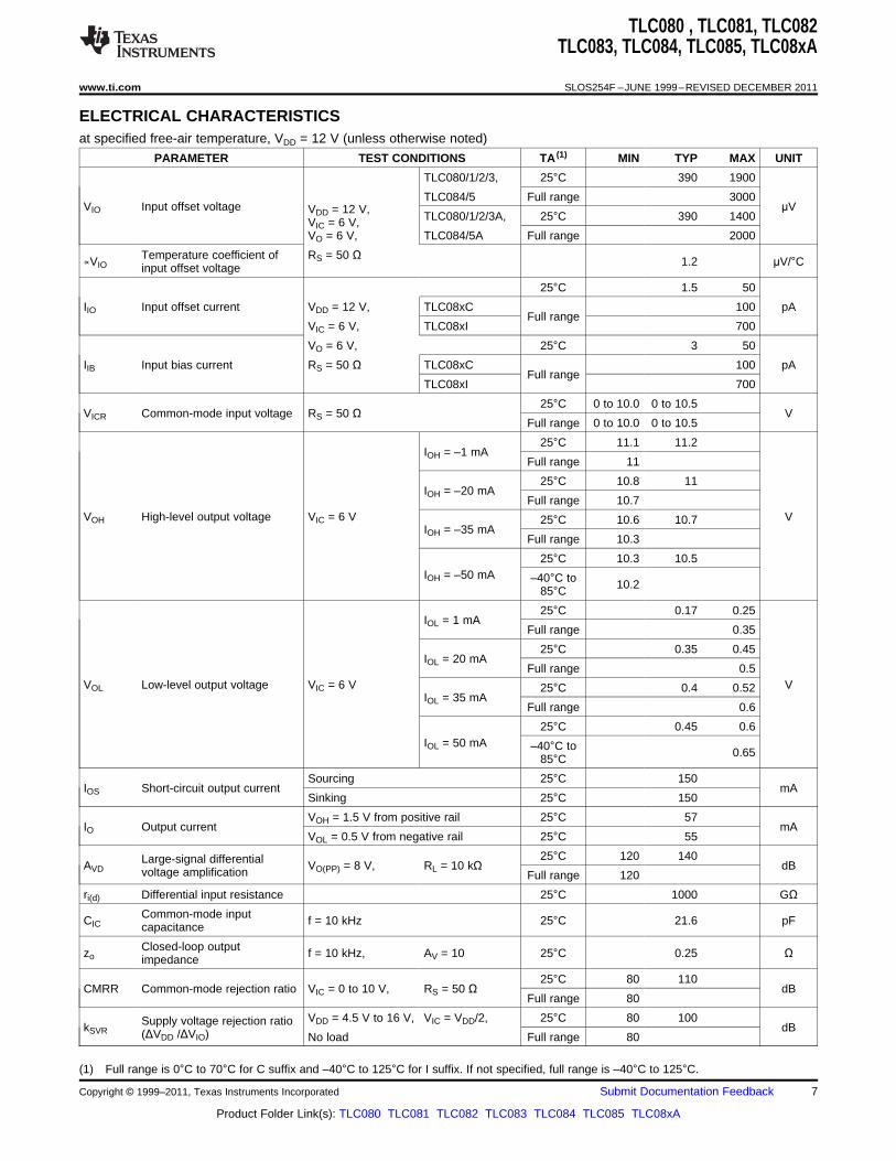
ELECTRICAL CHARACTERISTICSat specified free-air temperature, VDD = 5 V (unless otherwise noted)
PARAMETER TEST CONDITIONS TA (1) MIN TYP MAX UNIT
TLC080/1/2/3, 25°C 390 1900
TLC084/5 Full range 3000VIO Input offset voltage µVVDD = 5 V,
TLC080/1/2/3A, 25°C 390 1400VIC = 2.5 V,VO = 2.5 V, TLC084/5A Full range 2000
Temperature coefficient of RS = 50 Ω∝VIO 1.2 µV/°Cinput offset voltage
25°C 1.9 50
IIO Input offset current VDD = 5 V, TLC08XC 100 pAFull range
VIC = 2.5 V, TLC08XI 700
VO = 2.5 V, 25°C 3 50
IIB Input bias current RS = 50 Ω TLC08XC 100 pAFull range
TLC08XI 700
25°C 0 to 3.0 0 to 3.5VICR Common-mode input voltage RS = 50 Ω V
Full range 0 to 3.0 0 to 3.5
25°C 4.1 4.3IOH = –1 mA
Full range 3.9
25°C 3.7 4IOH = –20 mA
Full range 3.5VOH High-level output voltage VIC = 2.5 V V25°C 3.4 3.8
IOH = –35 mAFull range 3.2
25°C 3.2 3.6IOH = –50 mA –40°C to 385°C
25°C 0.18 0.25IOL = 1 mA
Full range 0.35
25°C 0.35 0.39IOL = 20 mA
Full range 0.45VOL Low-level output voltage VIC = 2.5 V V25°C 0.43 0.55
IOL = 35 mAFull range 0.7
25°C 0.45 0.63IOL = 50 mA –40°C to 0.785°C
Sourcing 25°C 100IOS Short-circuit output current mA
Sinking 25°C 100
VOH = 1.5 V from positive rail 25°C 57IO Output current mA
VOL = 0.5 V from negative rail 25°C 55
25°C 100 120Large-signal differentialAVD VO(PP) = 3 V, RL = 10 kΩ dBvoltage amplification Full range 100
ri(d) Differential input resistance 25°C 1000 GΩCommon-mode inputCIC f = 10 kHz 25°C 22.9 pFcapacitance
Closed-loop outputzo f = 10 kHz, AV = 10 25°C 0.25 Ωimpedance
25°C 80 110CMRR Common-mode rejection ratio VIC = 0 to 3 V, RS = 50 Ω dB
Full range 80
VDD = 4.5 V to 16 V, VIC = VDD/2, 25°C 80 100Supply voltage rejection ratiokSVR dB(ΔVDD /ΔVIO) No load Full range 80
(1) Full range is 0°C to 70°C for C suffix and –40°C to 125°C for I suffix. If not specified, full range is –40°C to 125°C.
Copyright © 1999–2011, Texas Instruments Incorporated Submit Documentation Feedback 5
Product Folder Link(s): TLC080 TLC081 TLC082 TLC083 TLC084 TLC085 TLC08xA

TLC080 , TLC081, TLC082TLC083, TLC084, TLC085, TLC08xA
SLOS254F –JUNE 1999–REVISED DECEMBER 2011 www.ti.com
ELECTRICAL CHARACTERISTICS (continued)at specified free-air temperature, VDD = 5 V (unless otherwise noted)
PARAMETER TEST CONDITIONS TA (1) MIN TYP MAX UNIT
25°C 1.8 2.5IDD Supply current (per channel) VO = 2.5 V, No load mA
Full range 3.5
Supply current in shutdown 25°C 125 200IDD(SHDN) mode (per channel) (TLC080, SHDN ≤ 0.8 V µA
Full range 250TLC083, TLC085)
OPERATING CHARACTERISTICSat specified free-air temperature, VDD = 5 V (unless otherwise noted)
PARAMETER TEST CONDITIONS TA(1) MIN TYP MAX UNIT
VO(PP) = 0.8 V, CL = 50 pF, 25°C 10 16Positive slew rate at unitySR+ V/µsgain RL = 10 kΩ Full range 9.5
VO(PP) = 0.8 V, CL = 50 pF, 25°C 12.5 19Negative slew rate at unitySR– V/µsgain RL = 10 kΩ Full range 10
f = 100 Hz 25°C 12Equivalent input noiseVn nV/√Hzvoltage f = 1 kHz 25°C 8.5
Equivalent input noiseIn f = 1 kHz 25°C 0.6 fA /√Hzcurrent
VO(PP) = 3 V, AV = 1 0.002Total harmonic distortionTHD + N RL = 10 kΩ and 250 Ω, AV = 10 25°C 0.012 %plus noise
f = 1 kHz AV = 100 0.085
t(on) Amplifier turnon time (2) 25°C 0.15 µsRL = 10 kΩ
t(off) Amplifier turnoff time (2) 25°C 1.3 µs
Gain-bandwidth product f = 10 kHz, RL = 10 kΩ 25°C 10 MHz
V(STEP)PP = 1 V, 0.1% 0.18AV = −1,CL = 10 pF, 0.01% 0.39RL = 10 kΩ
ts Settling time 25°C µsV(STEP)PP = 1 V, 0.1% 0.18AV = –1,CL = 47 pF, 0.01% 0.39RL = 10 kΩRL = 10 kΩ, CL = 50 pF 32
φm Phase margin 25°C °RL = 10 kΩ, CL = 0 pF 40
RL = 10 kΩ, CL = 50 pF 2.2Gain margin 25°C dB
RL = 10 kΩ, CL = 0 pF 3.3
(1) Full range is 0°C to 70°C for C suffix and –40°C to 125°C for I suffix. If not specified, full range is –40°C to 125°C.(2) Disable time and enable time are defined as the interval between application of the logic signal to SHDN and the point at which the
supply current has reached half its final value.
6 Submit Documentation Feedback Copyright © 1999–2011, Texas Instruments Incorporated
Product Folder Link(s): TLC080 TLC081 TLC082 TLC083 TLC084 TLC085 TLC08xA
TLC080 , TLC081, TLC082TLC083, TLC084, TLC085, TLC08xA
www.ti.com SLOS254F –JUNE 1999–REVISED DECEMBER 2011
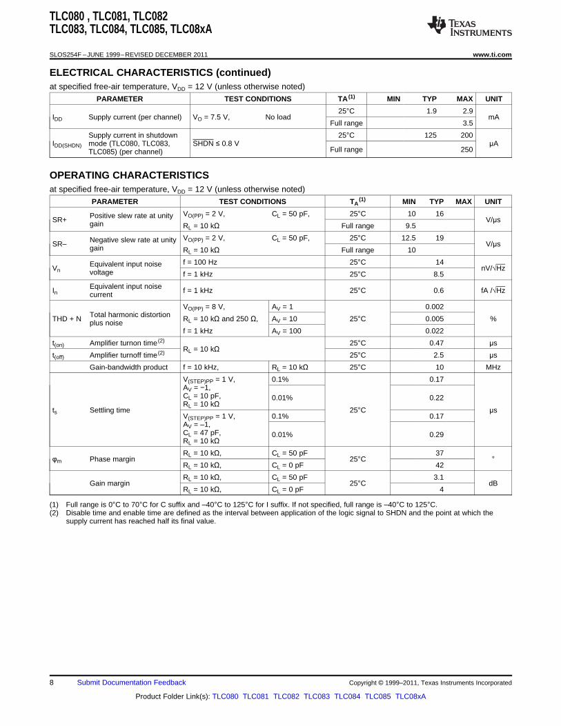
ELECTRICAL CHARACTERISTICSat specified free-air temperature, VDD = 12 V (unless otherwise noted)
PARAMETER TEST CONDITIONS TA (1) MIN TYP MAX UNIT
TLC080/1/2/3, 25°C 390 1900
TLC084/5 Full range 3000VIO Input offset voltage µVVDD = 12 V,
TLC080/1/2/3A, 25°C 390 1400VIC = 6 V,VO = 6 V, TLC084/5A Full range 2000
Temperature coefficient of RS = 50 Ω∝VIO 1.2 µV/°Cinput offset voltage
25°C 1.5 50
IIO Input offset current VDD = 12 V, TLC08xC 100 pAFull range
VIC = 6 V, TLC08xI 700
VO = 6 V, 25°C 3 50
IIB Input bias current RS = 50 Ω TLC08xC 100 pAFull range
TLC08xI 700
25°C 0 to 10.0 0 to 10.5VICR Common-mode input voltage RS = 50 Ω V
Full range 0 to 10.0 0 to 10.5
25°C 11.1 11.2IOH = –1 mA
Full range 11
25°C 10.8 11IOH = –20 mA
Full range 10.7VOH High-level output voltage VIC = 6 V V25°C 10.6 10.7
IOH = –35 mAFull range 10.3
25°C 10.3 10.5IOH = –50 mA –40°C to 10.285°C
25°C 0.17 0.25IOL = 1 mA
Full range 0.35
25°C 0.35 0.45IOL = 20 mA
Full range 0.5VOL Low-level output voltage VIC = 6 V V25°C 0.4 0.52
IOL = 35 mAFull range 0.6
25°C 0.45 0.6IOL = 50 mA –40°C to 0.6585°C
Sourcing 25°C 150IOS Short-circuit output current mA
Sinking 25°C 150
VOH = 1.5 V from positive rail 25°C 57IO Output current mA
VOL = 0.5 V from negative rail 25°C 55
25°C 120 140Large-signal differentialAVD VO(PP) = 8 V, RL = 10 kΩ dBvoltage amplification Full range 120
ri(d) Differential input resistance 25°C 1000 GΩCommon-mode inputCIC f = 10 kHz 25°C 21.6 pFcapacitance
Closed-loop outputzo f = 10 kHz, AV = 10 25°C 0.25 Ωimpedance
25°C 80 110CMRR Common-mode rejection ratio VIC = 0 to 10 V, RS = 50 Ω dB
Full range 80
VDD = 4.5 V to 16 V, VIC = VDD/2, 25°C 80 100Supply voltage rejection ratiokSVR dB(ΔVDD /ΔVIO) No load Full range 80
(1) Full range is 0°C to 70°C for C suffix and –40°C to 125°C for I suffix. If not specified, full range is –40°C to 125°C.
Copyright © 1999–2011, Texas Instruments Incorporated Submit Documentation Feedback 7
Product Folder Link(s): TLC080 TLC081 TLC082 TLC083 TLC084 TLC085 TLC08xA
TLC080 , TLC081, TLC082TLC083, TLC084, TLC085, TLC08xA
SLOS254F –JUNE 1999–REVISED DECEMBER 2011 www.ti.com
ELECTRICAL CHARACTERISTICS (continued)at specified free-air temperature, VDD = 12 V (unless otherwise noted)
PARAMETER TEST CONDITIONS TA (1) MIN TYP MAX UNIT
25°C 1.9 2.9IDD Supply current (per channel) VO = 7.5 V, No load mA
Full range 3.5
Supply current in shutdown 25°C 125 200IDD(SHDN) mode (TLC080, TLC083, SHDN ≤ 0.8 V µA
Full range 250TLC085) (per channel)
OPERATING CHARACTERISTICSat specified free-air temperature, VDD = 12 V (unless otherwise noted)
PARAMETER TEST CONDITIONS TA(1) MIN TYP MAX UNIT
VO(PP) = 2 V, CL = 50 pF, 25°C 10 16Positive slew rate at unitySR+ V/µsgain RL = 10 kΩ Full range 9.5
VO(PP) = 2 V, CL = 50 pF, 25°C 12.5 19Negative slew rate at unitySR– V/µsgain RL = 10 kΩ Full range 10
f = 100 Hz 25°C 14Equivalent input noiseVn nV/√Hzvoltage f = 1 kHz 25°C 8.5
Equivalent input noiseIn f = 1 kHz 25°C 0.6 fA /√Hzcurrent
VO(PP) = 8 V, AV = 1 0.002Total harmonic distortionTHD + N RL = 10 kΩ and 250 Ω, AV = 10 25°C 0.005 %plus noise
f = 1 kHz AV = 100 0.022
t(on) Amplifier turnon time (2) 25°C 0.47 µsRL = 10 kΩ
t(off) Amplifier turnoff time (2) 25°C 2.5 µs
Gain-bandwidth product f = 10 kHz, RL = 10 kΩ 25°C 10 MHz
V(STEP)PP = 1 V, 0.1% 0.17AV = −1,CL = 10 pF, 0.01% 0.22RL = 10 kΩ
ts Settling time 25°C µsV(STEP)PP = 1 V, 0.1% 0.17AV = –1,CL = 47 pF, 0.01% 0.29RL = 10 kΩRL = 10 kΩ, CL = 50 pF 37
φm Phase margin 25°C °RL = 10 kΩ, CL = 0 pF 42
RL = 10 kΩ, CL = 50 pF 3.1Gain margin 25°C dB
RL = 10 kΩ, CL = 0 pF 4
(1) Full range is 0°C to 70°C for C suffix and –40°C to 125°C for I suffix. If not specified, full range is –40°C to 125°C.(2) Disable time and enable time are defined as the interval between application of the logic signal to SHDN and the point at which the
supply current has reached half its final value.
8 Submit Documentation Feedback Copyright © 1999–2011, Texas Instruments Incorporated
Product Folder Link(s): TLC080 TLC081 TLC082 TLC083 TLC084 TLC085 TLC08xA

TLC080 , TLC081, TLC082TLC083, TLC084, TLC085, TLC08xA
www.ti.com SLOS254F –JUNE 1999–REVISED DECEMBER 2011
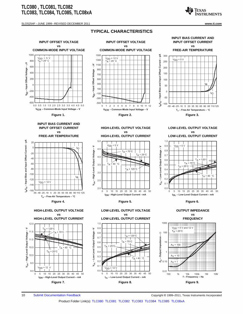
TYPICAL CHARACTERISTICS
Table of GraphsFIGURE
VIO Input offset voltage vs Common-mode input voltage 1, 2
IIO Input offset current vs Free-air temperature 3, 4
IIB Input bias current vs Free-air temperature 3, 4
VOH High-level output voltage vs High-level output current 5, 7
VOL Low-level output voltage vs Low-level output current 6, 8
Zo Output impedance vs Frequency 9
IDD Supply current vs Supply voltage 10
PSRR Power supply rejection ratio vs Frequency 11
CMRR Common-mode rejection ratio vs Frequency 12
Vn Equivalent input noise voltage vs Frequency 13
VO(PP) Peak-to-peak output voltage vs Frequency 14, 15
Crosstalk vs Frequency 16
Differential voltage gain vs Frequency 17, 18
Phase vs Frequency 17, 18
φm Phase margin vs Load capacitance 19, 20
Gain margin vs Load capacitance 21, 22
Gain-bandwidth product vs Supply voltage 23
vs Supply voltage 24SR Slew rate vs Free-air temperature 25, 26
vs Frequency 27, 28THD + N Total harmonic distortion plus noise
vs Peak-to-peak output voltage 29, 30
Large-signal follower pulse response 31, 32
Small-signal follower pulse response 33
Large-signal inverting pulse response 34, 35
Small-signal inverting pulse response 36
Shutdown forward isolation vs Frequency 37, 38
Shutdown reverse isolation vs Frequency 39, 40
vs Supply voltage 41Shutdown supply current
vs Free-air temperature 42
Shutdown pulse 43, 44
Copyright © 1999–2011, Texas Instruments Incorporated Submit Documentation Feedback 9
Product Folder Link(s): TLC080 TLC081 TLC082 TLC083 TLC084 TLC085 TLC08xA
0
-200
-400
-600
0.0 0.5 1.0 1.5 2.0 2.5 3.0
200
400
600
800
1000
3.5 4.0 4.5 5.0
VICR – Common-Mode Input Voltage – V
VDD = 5 V
TA = 25° C
VIO
–In
pu
tO
ffset
Vo
ltag
eV
–m
300
100
-100
-300
-500
0 1 2 3 4 5 6
500
700
900
1100
1500
1300
VICR – Common-Mode Input Voltage – V
VIO
–In
pu
tO
ffset
Vo
ltag
eV
- m
VDD = 12 V
TA = 25° C
7 8 9 10 11 12 I/I
–In
pu
t B
ias
an
d I
np
ut
Off
se
t C
urr
en
t–
pA
IBIO
T – Free-Air Temperature – CA °
-100
-55 -40
50
200
-10 5
150
100
-50
-25 20 35 50
IIB
VDD = 5 V
65 80 95 110125
250
300
IIO0
2.0
2.5
3.0
3.5
4.0
4.5
5.0
0 5 10 15 20 25 30 35 40 45 50
IOH - High-Level Output Current - mA
VDD = 5 V
TA = 125°C
TA = 70°C
TA = 25°C
TA = 40 °C
V–
Hig
h-L
ev
el
Ou
tpu
t V
olt
ag
e–
VO
H
0.0
0.1
0.2
0.3
0.4
0.5
0.6
0.7
0.8
0.9
1.0
0 5 10 15 20 25 30 35 40 45 50
IOL – Low-Level Output Current – mA
TA = 125°C
TA = 70°C
TA = 25°C
TA = 40 °C
VDD = 5 V
V–
Lo
w-L
ev
el
Ou
tpu
t V
olt
ag
e–
VO
L
-120
-55 -40
-80
-20
-10 5
IIO
-40
-60
-100
-25
-140
-160
20 35 50
IIB
VDD = 12 V
65 80 95 110 125
0
20
T – Free-Air Temperature – °CA
I/I
–In
pu
t B
ias
an
d I
np
ut
Off
se
t C
urr
en
t–
pA
IBIO
f – Frequency – Hz100k
1000
1M 10M10k100 1k
100
10
1
0.10
0.01
AV = 100
AV = 1
AV = 10
VDD = 5 V and 12 V
TA = 25°C
Z–
Ou
tpu
t Im
ped
an
ce
–O
W
9.0
9.5
10.0
10.5
11.0
11.5
12.0
0 5 10 15 20 25 30 35 40 45 50
IOH – High-Level Output Current – mA
TA = 125°C
TA = 70°C
TA = 25°C
TA = 40 °C
VDD = 12 V
V–
Hig
h-L
ev
el
Ou
tpu
t V
olt
ag
e–
VO
H
0.0
0.1
0.2
0.3
0.4
0.5
0.6
0.7
0.8
0.9
1.0
0 5 10 15 20 25 30 35 40 45 50
TA = 125°C
TA = 25°C
TA = 40 °C
VDD = 12 V
TA = 70°C
V–
Lo
w-L
ev
el
Ou
tpu
t V
olt
ag
e–
VO
L
I – Low-Level Output Current – mAOL
TLC080 , TLC081, TLC082TLC083, TLC084, TLC085, TLC08xA
SLOS254F –JUNE 1999–REVISED DECEMBER 2011 www.ti.com
TYPICAL CHARACTERISTICSINPUT BIAS CURRENT AND
INPUT OFFSET VOLTAGE INPUT OFFSET VOLTAGE INPUT OFFSET CURRENTvs vs vs
COMMON-MODE INPUT VOLTAGE COMMON-MODE INPUT VOLTAGE FREE-AIR TEMPERATURE
Figure 1. Figure 2. Figure 3.
INPUT BIAS CURRENT ANDINPUT OFFSET CURRENT HIGH-LEVEL OUTPUT VOLTAGE LOW-LEVEL OUTPUT VOLTAGE
vs vs vsFREE-AIR TEMPERATURE HIGH-LEVEL OUTPUT CURRENT LOW-LEVEL OUTPUT CURRENT
Figure 4. Figure 5. Figure 6.
HIGH-LEVEL OUTPUT VOLTAGE LOW-LEVEL OUTPUT VOLTAGE OUTPUT IMPEDANCEvs vs vs
HIGH-LEVEL OUTPUT CURRENT LOW-LEVEL OUTPUT CURRENT FREQUENCY
Figure 7. Figure 8. Figure 9.
10 Submit Documentation Feedback Copyright © 1999–2011, Texas Instruments Incorporated
Product Folder Link(s): TLC080 TLC081 TLC082 TLC083 TLC084 TLC085 TLC08xA

0
20
40
60
80
100
120
140
f – Frequency – Hz
100k 1M 10M10k100 1k
CM
RR
–C
om
mo
n-M
od
e R
eje
cti
on
Rati
o–
dB
VDD = 5 V and 12 V
TA = 25°C
40
0 10
80
140
1k 10k
VDD = 12 V
120
100
60
100
20
0
–P
ow
er
Su
pp
ly R
eje
cti
on
Rati
o–
dB
PS
RR
100k 1M 10M
VDD = 5 V
f – Frequency – Hz
1.0
1.2
1.4
1.6
1.8
2.0
2.2
2.4
4 5 6 7 8 9 10 11 12 13 14 15
TA = 40 °C
AV = 1
SHDN = VDD
Per Channel
TA = 125°C
TA = 70°C
TA = 25°C
V – Supply Voltage – VDD
I–
Su
pp
ly C
urr
en
t–
mA
DD
0
2
4
6
8
10
12
f – Frequency – Hz
100k 1M 10M10k
THD+N < = 5%
RL = 600 Ω
TA = 25°C
VDD = 12 V
VDD = 5 V
VO
(PP
)–
Peak-t
o-P
eak
Ou
tpu
tV
olt
ag
e–
V
0
2
4
6
8
10
12
f – Frequency – H
100k 1M 10M10k
VO
(PP
)–
Peak-t
o-P
eak
Ou
tpu
tV
olt
ag
e–
V
THD+N < = 5%
RL= 10 kΩ
TA = 25°C
VDD = 12 V
VDD = 5 V
0
10 100
10
25
10k 100k
f – Frequency – Hz
VDD = 5 V
40
VDD = 12 V
35
30
20
15
5
1k
nV
/H
z–
Eq
uiv
ale
nt
Inp
ut
No
ise
Vo
ltag
e–
Vn
-120
10 100
-80
-20
10k
f – Frequency – Hz
0
-40
-60
-100
1k
-140
-160
Cro
ssta
lk–
dB
100k
VDD = 5 V and 12 V
AV = 1
RL = 10 kΩ
VI(PP) = 2 V
For All Channels
TLC080 , TLC081, TLC082TLC083, TLC084, TLC085, TLC08xA
www.ti.com SLOS254F –JUNE 1999–REVISED DECEMBER 2011
TYPICAL CHARACTERISTICSPOWER SUPPLY REJECTION
SUPPLY CURRENT RATIO COMMON-MODE REJECTION RATIOvs vs vs
SUPPLY VOLTAGE FREQUENCY FREQUENCY
Figure 10. Figure 11. Figure 12.
PEAK-TO-PEAK OUTPUT PEAK-TO-PEAK OUTPUTEQUIVALENT INPUT NOISEVOLTAGE VOLTAGE VOLTAGE
vs vs vsFREQUENCY FREQUENCY FREQUENCY
Figure 13. Figure 14. Figure 15.
CROSSTALKvs
FREQUENCY
Figure 16.
Copyright © 1999–2011, Texas Instruments Incorporated Submit Documentation Feedback 11
Product Folder Link(s): TLC080 TLC081 TLC082 TLC083 TLC084 TLC085 TLC08xA

0
1k 10k
20
50
1M 10M
f – Frequency – Hz
Gain
80
70
60
40
30
10
100k
-10
-20
–D
iffe
ren
tVo
ltag
eG
ain
–d
BA
VD
100M
-180
-135
0
-45
-90
-225
Phase
VDD = ±2.5 VRL = 10 kΩCL = 0 pFTA = 25°C
Ph
ase
–°
0
1k 10k
20
50
1M 10M
f – Frequency – Hz
Gain
80
70
60
40
30
10
100k
-10
-20
–D
iffe
ren
tVo
ltag
eG
ain
–d
BA
VD
100M
-180
-135
0
-45
-90
-225
Phase
VDD = ±6 VRL = 10 kΩCL = 0 pF TA= 25°C
Ph
ase
–°
10°
10
20°
35°
CL – Load Capacitance – pF
30°
25°
15°
100
5°
0°
Rnull = 0 Ω
Rnull = 20 Ω
Rnull = 50 Ω
Rnull = 100 Ω
VDD = 5 V
RL = 10 kΩ
TA = 25°C
40°
mφ
–P
hase M
arg
in
10°
10
20°
35°
CL – Load Capacitance – pF
30°
25°
15°
100
5°
0°
Rnull = 0 Ω
Rnull = 20 Ω
Rnull = 50 Ω
Rnull = 100 Ω
VDD = 12 V
RL = 10 kΩ
TA = 25°C
40°
45°
mφ
–P
hase
Marg
in
1
10
2
4
CL – Load Capacitance – pF
3.5
2.5
1.5
100
0.5
0
–G
ain
Marg
in–
dB
G
Rnull = 0 Ω
Rnull = 20 Ω
Rnull = 50 Ω
Rnull = 100 Ω
VDD = 5 V
RL = 10 kΩ
TA = 25°C
3
9.0
9.1
9.2
9.3
9.4
9.5
9.6
9.7
9.8
9.9
10.0
4 5 6 7 8 9 10 11 12 13 14 15 16
CL = 11 pF
TA = 25°C
VDD – Supply Voltage – V
GB
WP
–G
ain
Ba
nd
wid
th P
rod
uc
t–
MH
z
RL = 10 kΩ
RL = 600 Ω
12
13
14
15
16
17
18
19
20
21
22
4 5 6 7 8 9 10 11 12 13 14 15 16
VDD – Supply Voltage – V
RL = 600 Ω and 10 kΩCL = 50 pFAV = 1
SR
–S
lew
Rate
–V
/ms
Slew Rate +
Slew Rate
1
10
2
3.5
CL – Load Capacitance – pF
3
2.5
1.5
100
0.5
0
Rnull = 0 Ω
Rnull = 20 Ω
Rnull = 50 Ω
Rnull = 100 Ω
VDD = 12 V
RL = 10 kΩ
TA = 25°C
4
4.5
5
mφ
–P
hase M
arg
in–
dB
TLC080 , TLC081, TLC082TLC083, TLC084, TLC085, TLC08xA
SLOS254F –JUNE 1999–REVISED DECEMBER 2011 www.ti.com
TYPICAL CHARACTERISTICSDIFFERENTIAL VOLTAGE GAIN AND DIFFERENTIAL VOLTAGE GAIN AND
PHASE PHASEvs vs
FREQUENCY FREQUENCY
Figure 17. Figure 18.
PHASE MARGIN PHASE MARGIN GAIN MARGINvs vs vs
LOAD CAPACITANCE LOAD CAPACITANCE LOAD CAPACITANCE
Figure 19. Figure 20. Figure 21.
GAIN MARGIN GAIN BANDWIDTH PRODUCT SLEW RATEvs vs vs
LOAD CAPACITANCE SUPPLY VOLTAGE SUPPLY VOLTAGE
Figure 22. Figure 23. Figure 24.
12 Submit Documentation Feedback Copyright © 1999–2011, Texas Instruments Incorporated
Product Folder Link(s): TLC080 TLC081 TLC082 TLC083 TLC084 TLC085 TLC08xA
0
5
10
15
20
25
-55 -35 -15 5 25 4 565 85 105 125
TA – Free-Air Temperature –°C
VDD = 5 VRL= 600 Ω and 10 kΩCL = 50 pFAV = 1
SR
–S
lew
Rate
–V
/ms
Slew Rate +
Slew Rate
0
5
10
15
20
25
-55 -35 -15 5 25 4 565 85 105 125
TA – Free-Air Temperature – °C
VDD = 12 VRL= 600 Ω and 10 kΩCL = 50 pFAV = 1
SR
–S
lew
Rate
–V
/ms
Slew Rate +
Slew Rate –
0.001
100 1k
0.01
0.1
10k 100k
f – Frequency– Hz
AV = 100
AV = 10
AV = 1
1
To
tal H
arm
on
ic D
isto
rtio
n +
No
ise
–% VDD = 5 V
VO(PP) = 2 V
RL = 10 kΩ
To
tal H
arm
on
ic D
isto
rtio
n +
No
ise
–%
0.001
100 1k
0.01
0.1
10k 100k
f – Frequency – Hz
AV = 100
VDD = 12 V
VO(PP) = 8 V
RL = 10 kΩ
AV = 10
AV = 1
To
tal H
arm
on
ic D
isto
rtio
n +
No
ise
–%
0.0001
0.25 0.75
0.01
0.1
1.25 1.75
VO(PP) – Peak-to-Peak Output Voltage – V
2.25 2.75 3.25 3.75
0.001
1
10VDD = 5 V
AV = 1
f = 1 kHz
RL = 250 Ω
RL = 600 Ω
RL = 10 kΩ
To
tal H
arm
on
ic D
isto
rtio
n +
No
ise
–%
0.0001
0.5 2.5
0.01
0.1
4.5 6.5
VO(PP) – Peak-to-Peak Output Voltage – V
8.5 10.5
0.001
1
10VDD = 12 V
AV = 1
f = 1 kHz
RL = 250 Ω
RL = 600 Ω
RL = 10 kΩ
t – Time – ms
0 0.2 0.4 0.6 0.8 1 1.2 1.4 1.6 1.8 2
–O
utp
ut
Vo
ltag
e–
VV
O
VI (1 V/Div)
VO (500 mV/Div)
VDD = 5 V
RL = 600 Ω
and 10 kΩ
CL = 8 pF
TA = 25°C
t – Time – ms
0 0.2 0.4 0.6 0.8 1 1.2 1.4 1.6 1.8 2
–O
utp
ut
Vo
ltag
e–
VV
O
VI (5 V/Div)
VO (2 V/Div)
VDD = 12 V
RL = 600 Ω
and 10 kΩ
CL = 8 pF
TA = 25°C
0 0.1 0.3 0.4
t – Time – ms
0 .2 0.5 0.6 0.7 0.8 0.9 0.10
VO(50mV/Div)
VI(100mV/Div)
VDD = 5 V and 12 VRL = 600Ω and 10 kΩCL = 8 pFTA = 25°C
–O
utp
ut
Vo
ltag
e–
VVO
.0
TLC080 , TLC081, TLC082TLC083, TLC084, TLC085, TLC08xA
www.ti.com SLOS254F –JUNE 1999–REVISED DECEMBER 2011
TYPICAL CHARACTERISTICSTOTAL HARMONIC DISTORTION
SLEW RATE SLEW RATE PLUS NOISEvs vs vs
FREE-AIR TEMPERATURE FREE-AIR TEMPERATURE FREQUENCY
Figure 25. Figure 26. Figure 27.
TOTAL HARMONIC DISTORTION TOTAL HARMONIC DISTORTION TOTAL HARMONIC DISTORTIONPLUS NOISE PLUS NOISE PLUS NOISE
vs vs vsFREQUENCY PEAK-TO-PEAK OUTPUT VOLTAGE PEAK-TO-PEAK OUTPUT VOLTAGE
Figure 28. Figure 29. Figure 30.
LARGE SIGNAL FOLLOWER LARGE SIGNAL FOLLOWER SMALL SIGNAL FOLLOWERPULSE RESPONSE PULSE RESPONSE PULSE RESPONSE
Figure 31. Figure 32. Figure 33.
Copyright © 1999–2011, Texas Instruments Incorporated Submit Documentation Feedback 13
Product Folder Link(s): TLC080 TLC081 TLC082 TLC083 TLC084 TLC085 TLC08xA

t – Time – ms
0 0.2 0.4 0.6 0.8 1 1.2 1.4 1.6 1.8 2
–O
utp
ut
Vo
ltag
e–
VVO
VI (2 V/div)
VO (500 mV/Div)
VDD = 5 V
RL = 600 Ω
and 10 kΩ
CL = 8 pF
TA = 25°C
t – Time – ms
0 0.2 0.4 0.6 0.8 1 1.2 1.4 1.6 1.8 2–
Ou
tpu
t V
olt
ag
e–
VV
O
VI (5 V/div)
VO (2 V/Div)
VDD = 12 V
RL = 600 Ω
and 10 kΩ
CL = 8 pF
TA = 25°C
t – Time – ms
0 0.1 0.2 0.3 0.4 0.5 0.6 0.7 0.8 0.9 1
–O
utp
ut
Vo
ltag
e–
VV
O
VI (100 mV/div)
VO (50 mV/Div)
VDD = 5 V and 12 V
RL = 600 Ω and 10 kΩ
CL = 8 pF
TA = 25°C
20
40
60
80
100
120
140
f – Frequency – Hz
100k 1M 10M10k100 1k
Su
tdo
wn
Fo
rward
Iso
lati
on
–d
B
100M
VDD = 12 V
CL= 0 pF
TA = 25°C
VI(PP) = 0.1, 8, 12 V
RL = 600 Ω
RL = 10 kΩ
20
40
60
80
100
120
140
f – Frequency – Hz
100k 1M 10M10k100 1k
Su
tdo
wn
Revers
eIs
ola
tio
n–
dB
100M
RL = 600 Ω
RL = 10 kΩ
VDD = 5 V
CL= 0 pF
TA = 25°C
VI(PP) = 0.1, 2.5, and 5 V
20
40
60
80
100
120
140
f – Frequency – Hz
100k 1M 10M10k100 1k
Su
tdo
wn
Fo
rward
Iso
lati
on
–d
B
100M
VDD = 5 V
CL= 0 pF
TA = 25°C
VI(PP) = 0.1, 2.5, and 5 V
RL = 600 Ω
RL = 10 kΩ
118
120
122
124
126
128
130
132
134
136
4 5 6 7 8 9 10 11 12 13 14 15 16
VDD – Supply Voltage – V
I DD
(SH
DN
)–
Sh
utd
ow
n S
up
ply
Cu
rren
t–
Am
Shutdown OnRL = openVIN = VDD/2
60
80
100
120
140
160
180
–55 –25 535 65 95 125
TA – Free-Air Temperature –°C
VDD = 12 V
AV = 1
VIN = VDD/2
I DD
(SH
DN
)–
Sh
utd
ow
n S
up
ply
Cu
rren
t–
Am
VDD = 5 V
20
40
60
80
100
120
140
f – Frequency – Hz
100k 1M 10M10k100 1k
Su
tdo
wn
Revers
eIs
ola
tio
n–
dB
100M
VDD = 12 V
CL= 0 pF
TA = 25°C
VI(PP) = 0.1, 8, 12 V
RL = 600 Ω
RL = 10 kΩ
TLC080 , TLC081, TLC082TLC083, TLC084, TLC085, TLC08xA
SLOS254F –JUNE 1999–REVISED DECEMBER 2011 www.ti.com
TYPICAL CHARACTERISTICSLARGE SIGNAL INVERTING LARGE SIGNAL INVERTING SMALL SIGNAL INVERTING
PULSE RESPONSE PULSE RESPONSE PULSE RESPONSE
Figure 34. Figure 35. Figure 36.
SHUTDOWN FORWARD SHUTDOWN FORWARD SHUTDOWN REVERSEISOLATION ISOLATION ISOLATION
vs vs vsFREQUENCY FREQUENCY FREQUENCY
Figure 37. Figure 38. Figure 39.
SHUTDOWN REVERSEISOLATION SHUTDOWN SUPPLY CURRENT SHUTDOWN SUPPLY CURRENT
vs vs vsFREQUENCY SUPPLY VOLTAGE FREE-AIR TEMPERATURE
Figure 40. Figure 41. Figure 42.
14 Submit Documentation Feedback Copyright © 1999–2011, Texas Instruments Incorporated
Product Folder Link(s): TLC080 TLC081 TLC082 TLC083 TLC084 TLC085 TLC08xA
0.0
0.5
1.0
1.5
2.0
2.5
3.0
3.5
4.0
4.5
5.0
5.5
6.0
0 10 20 30 40 50 60 70 80
-2
-4
2
6
t – Time – ms
0
-6
4Shutdown Pulse
SD Off
VDD = 5 V
CL= 8 pF
TA = 25°C
IDD RL = 600 Ω
IDD RL = 10 kΩ
I DD
–S
up
ply
Cu
rren
t–
mA
Sh
utd
ow
nP
uls
e-
V
0.0
0.5
1.0
1.5
2.0
2.5
3.0
3.5
4.0
4.5
5.0
5.5
6.0
0 10 20 30 40 50 60 70 80
-2
-4
2
6
t – Time – ms
0
-6
4Shutdown Pulse
SD Off
VDD = 12 V
CL= 8 pF
TA = 25°C
IDD RL = 600 Ω
IDD RL = 10 kΩ
I DD
–S
up
ply
Cu
rren
t–
mA
Sh
utd
ow
nP
uls
e-
V
_
+
Rnull
RL CL
Figure 45
N1
100 kΩ
+ N2
R1
VDD
OUT
IN
IN+
TLC080 , TLC081, TLC082TLC083, TLC084, TLC085, TLC08xA
www.ti.com SLOS254F –JUNE 1999–REVISED DECEMBER 2011
TYPICAL CHARACTERISTICSSHUTDOWN PULSE SHUTDOWN PULSE
Figure 43. Figure 44.
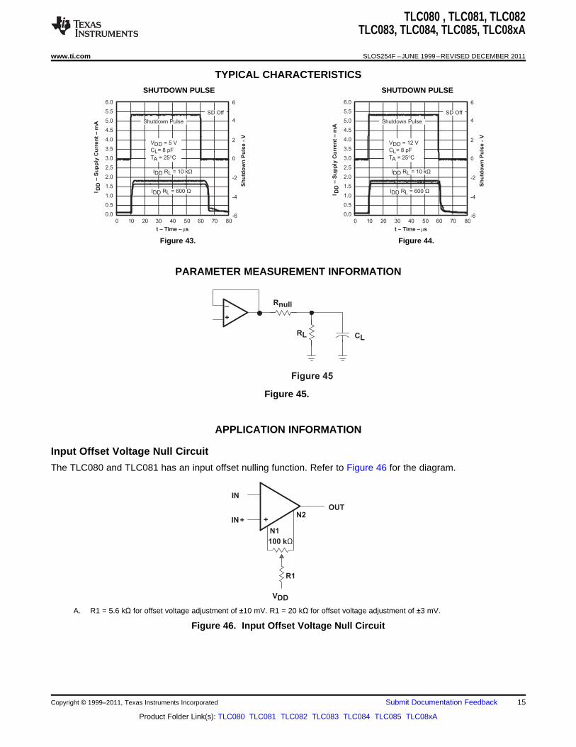
PARAMETER MEASUREMENT INFORMATION
Figure 45.
APPLICATION INFORMATION
Input Offset Voltage Null Circuit
The TLC080 and TLC081 has an input offset nulling function. Refer to Figure 46 for the diagram.
A. R1 = 5.6 kΩ for offset voltage adjustment of ±10 mV. R1 = 20 kΩ for offset voltage adjustment of ±3 mV.
Figure 46. Input Offset Voltage Null Circuit
Copyright © 1999–2011, Texas Instruments Incorporated Submit Documentation Feedback 15
Product Folder Link(s): TLC080 TLC081 TLC082 TLC083 TLC084 TLC085 TLC08xA

CLOAD
RF
InputOutput
RGRNULL_
+
VOO
VIO
1R
F
RG
IIB
RS
1RF
RG
IIB–
RF
+VI
+
RG
RS
RF
IIB–
VO
IIB+
= ( ))( ± + ( ))( ±+ +
TLC080 , TLC081, TLC082TLC083, TLC084, TLC085, TLC08xA
SLOS254F –JUNE 1999–REVISED DECEMBER 2011 www.ti.com
Driving a Capacitive Load
When the amplifier is configured in this manner, capacitive loading directly on the output will decrease thedevice’s phase margin leading to high frequency ringing or oscillations. Therefore, for capacitive loads of greaterthan 10 pF, it is recommended that a resistor be placed in series (RNULL) with the output of the amplifier, asshown in Figure 47. A minimum value of 20 Ω should work well for most applications.
Figure 47. Driving a Capacitive Load
Offset Voltage
The output offset voltage, (VOO) is the sum of the input offset voltage (VIO) and both input bias currents (IIB) timesthe corresponding gains. The following schematic and formula can be used to calculate the output offset voltage:
Figure 48. Output Offset Voltage Model
16 Submit Documentation Feedback Copyright © 1999–2011, Texas Instruments Incorporated
Product Folder Link(s): TLC080 TLC081 TLC082 TLC083 TLC084 TLC085 TLC08xA

_
+
600 Ω 22 pF50 Ω
10 kΩ
10 pF
IN
WithCF = 10 pF
VDD = ±5 VAV = +1RF = 10 kΩRL = 600 ΩCL = 22 pF
0
0.5
1
1.5
1
0
1
2
0 0.2 0.4 0.6 0.8 1 1.2 1.4 1.6
t - Time - ms
VIN
VOUT
0.5
V–
Inp
ut
Vo
ltag
e–
VI
V–
Ou
tpu
t V
olt
ag
e–
VO
TLC080 , TLC081, TLC082TLC083, TLC084, TLC085, TLC08xA
www.ti.com SLOS254F –JUNE 1999–REVISED DECEMBER 2011
High Speed CMOS Input Amplifiers
The TLC08x is a family of high-speed low-noise CMOS input operational amplifiers that has an input capacitanceof the order of 20 pF. Any resistor used in the feedback path adds a pole in the transfer function equivalent to theinput capacitance multiplied by the combination of source resistance and feedback resistance. For example, again of –10, a source resistance of 1 kΩ, and a feedback resistance of 10 kΩ add an additional pole atapproximately 8 MHz. This is more apparent with CMOS amplifiers than bipolar amplifiers due to their greaterinput capacitance.
This is of little consequence on slower CMOS amplifiers, as this pole normally occurs at frequencies above theirunity-gain bandwidth. However, the TLC08x with its 10-MHz bandwidth means that this pole normally occurs atfrequencies where there is on the order of 5dB gain left and the phase shift adds considerably.
The effect of this pole is the strongest with large feedback resistances at small closed loop gains. As thefeedback resistance is increased, the gain peaking increases at a lower frequency and the 180° phase shiftcrossover point also moves down in frequency, decreasing the phase margin.
For the TLC08x, the maximum feedback resistor recommended is 5 kΩ; larger resistances can be used but acapacitor in parallel with the feedback resistor is recommended to counter the effects of the input capacitancepole.
The TLC083 with a 1-V step response has an 80% overshoot with a natural frequency of 3.5 MHz whenconfigured as a unity gain buffer and with a 10-kΩ feedback resistor. By adding a 10-pF capacitor in parallel withthe feedback resistor, the overshoot is reduced to 40% and eliminates the natural frequency, resulting in a muchfaster settling time (see Figure 49). The 10-pF capacitor was chosen for convenience only.
Load capacitance had little effect on these measurements due to the excellent output drive capability of theTLC08x.
Figure 49. 1-V Step Response
Copyright © 1999–2011, Texas Instruments Incorporated Submit Documentation Feedback 17
Product Folder Link(s): TLC080 TLC081 TLC082 TLC083 TLC084 TLC085 TLC08xA

VI
VO
C1
+
RG RF
R1
f–3dB
1
2pR1C1
VO
VI
1
RF
RG
1
1 sR1C1= ( + )( )+
=
VI
C2
R2R1
C1
RFRG
R1 = R2 = R
C1 = C2 = C
Q = Peaking Factor
(Butterworth Q = 0.707)
(
=1
Q2 )
RGRF
_
+
f–3dB
12pRC
–
=
TLC080 , TLC081, TLC082TLC083, TLC084, TLC085, TLC08xA
SLOS254F –JUNE 1999–REVISED DECEMBER 2011 www.ti.com
General Configurations
When receiving low-level signals, limiting the bandwidth of the incoming signals into theFigure 50 system is oftenrequired. The simplest way to accomplish this is to place an RC filter at the noninverting terminal of the amplifier(see ).
Figure 50. Single-Pole Low-Pass Filter
If even more attenuation is needed, a multiple pole filter is required. The Sallen-Key filter can be used for thistask. For best results, the amplifier should have a bandwidth that is 8 to 10 times the filter frequency bandwidth.Failure to do this can result in phase shift of the amplifier.
Figure 51. 2-Pole Low-Pass Sallen-Key Filter
18 Submit Documentation Feedback Copyright © 1999–2011, Texas Instruments Incorporated
Product Folder Link(s): TLC080 TLC081 TLC082 TLC083 TLC084 TLC085 TLC08xA
TLC080 , TLC081, TLC082TLC083, TLC084, TLC085, TLC08xA
www.ti.com SLOS254F –JUNE 1999–REVISED DECEMBER 2011
Shutdown Function
Three members of the TLC08x family (TLC080/3/5) have a shutdown terminal (SHDN) for conserving battery lifein portable applications. When the shutdown terminal is tied low, the supply current is reduced to125 µA/channel, the amplifier is disabled, and the outputs are placed in a high-impedance mode. To enable theamplifier, the shutdown terminal can either be left floating or pulled high. When the shutdown terminal is leftfloating, care should be taken to ensure that parasitic leakage current at the shutdown terminal does notinadvertently place the operational amplifier into shutdown. The shutdown terminal threshold is alwaysreferenced to the voltage on the GND terminal of the device. Therefore, when operating the device with splitsupply voltages (e.g. ±2.5 V), the shutdown terminal needs to be pulled to VDD– (not system ground) to disablethe operational amplifier.
The amplifier’s output with a shutdown pulse is shown in Figure 43 and Figure 44. The amplifier is powered witha single 5-V supply and is configured as noninverting with a gain of 5. The amplifier turnon and turnoff times aremeasured from the 50% point of the shutdown pulse to the 50% point of the output waveform. The times for thesingle, dual, and quad are listed in the data tables.
Figure 37 through Figure 40 show the amplifiers forward and reverse isolation in shutdown. The operationalamplifier is configured as a voltage follower (AV = 1). The isolation performance is plotted across frequency using0.1 VPP, 2.5 VPP, and 5 VPP input signals at ±2.5 V supplies and 0.1 VPP, 8 VPP, and 12 VPP input signals at ±6 Vsupplies.
Circuit Layout Considerations
To achieve the levels of high performance of the TLC08x, follow proper printed-circuit board design techniques.A general set of guidelines is given in the following.• Ground planes – It is highly recommended that a ground plane be used on the board to provide all
components with a low inductive ground connection. However, in the areas of the amplifier inputs and output,the ground plane can be removed to minimize the stray capacitance.
• Proper power supply decoupling – Use a 6.8-µF tantalum capacitor in parallel with a 0.1-µF ceramic capacitoron each supply terminal. It may be possible to share the tantalum among several amplifiers depending on theapplication, but a 0.1-µF ceramic capacitor should always be used on the supply terminal of every amplifier.In addition, the 0.1-µF capacitor should be placed as close as possible to the supply terminal. As this distanceincreases, the inductance in the connecting trace makes the capacitor less effective. The designer shouldstrive for distances of less than 0.1 inches between the device power terminals and the ceramic capacitors.
• Sockets – Sockets can be used but are not recommended. The additional lead inductance in the socket pinswill often lead to stability problems. Surface-mount packages soldered directly to the printed-circuit board isthe best implementation.
• Short trace runs/compact part placements – Optimum high performance is achieved when stray seriesinductance has been minimized. To realize this, the circuit layout should be made as compact as possible,thereby minimizing the length of all trace runs. Particular attention should be paid to the inverting input of theamplifier. Its length should be kept as short as possible. This will help to minimize stray capacitance at theinput of the amplifier.
• Surface-mount passive components – Using surface-mount passive components is recommended for highperformance amplifier circuits for several reasons. First, because of the extremely low lead inductance ofsurface-mount components, the problem with stray series inductance is greatly reduced. Second, the smallsize of surface-mount components naturally leads to a more compact layout thereby minimizing both strayinductance and capacitance. If leaded components are used, it is recommended that the lead lengths be keptas short as possible.
Copyright © 1999–2011, Texas Instruments Incorporated Submit Documentation Feedback 19
Product Folder Link(s): TLC080 TLC081 TLC082 TLC083 TLC084 TLC085 TLC08xA

DIE
Side View (a)
End View (b)Bottom View (c)
DIE
Thermal
Pad
TLC080 , TLC081, TLC082TLC083, TLC084, TLC085, TLC08xA
SLOS254F –JUNE 1999–REVISED DECEMBER 2011 www.ti.com
General PowerPAD Design Considerations
The TLC08x is available in a thermally-enhanced PowerPAD family of packages. These packages areconstructed using a downset leadframe upon which the die is mounted [see Figure 52(a) and Figure 52(b)]. Thisarrangement results in the lead frame being exposed as a thermal pad on the underside of the package [seeFigure 52(c)]. Because this thermal pad has direct thermal contact with the die, excellent thermal performancecan be achieved by providing a good thermal path away from the thermal pad.
A. The thermal pad is electrically isolated from all terminals in the package.
Figure 52. Views of Thermally-Enhanced DGN Package
The PowerPAD package allows for both assembly and thermal management in one manufacturing operation.During the surface-mount solder operation (when the leads are being soldered), the thermal pad must besoldered to a copper area underneath the package. Through the use of thermal paths within this copper area,heat can be conducted away from the package into either a ground plane or other heat dissipating device.Soldering the PowerPAD to the printed circuit board (PCB) is always required, even with applicationsthat have low power dissipation. This soldering provides the necessary thermal and mechanical connectionbetween the lead frame die pad and the PCB.
Although there are many ways to properly heatsink the PowerPAD package, the following steps illustrate therecommended approach.
20 Submit Documentation Feedback Copyright © 1999–2011, Texas Instruments Incorporated
Product Folder Link(s): TLC080 TLC081 TLC082 TLC083 TLC084 TLC085 TLC08xA
TAMAX
D
JA
T -P =
θ
æ öç ÷è ø
TLC080 , TLC081, TLC082TLC083, TLC084, TLC085, TLC08xA
www.ti.com SLOS254F –JUNE 1999–REVISED DECEMBER 2011
The PowerPAD must be connected to the most negative supply voltage (GND pin potential) of the device.1. Prepare the PCB with a top side etch pattern (see the landing patterns at the end of this data sheet). There
should be etch for the leads as well as etch for the thermal pad.2. Place five holes (dual) or nine holes (quad) in the area of the thermal pad. These holes should be 13 mils in
diameter. Keep them small so that solder wicking through the holes is not a problem during reflow.3. Additional vias may be placed anywhere along the thermal plane outside of the thermal pad area. This helps
dissipate the heat generated by the TLC08x IC. These additional vias may be larger than the 13-mil diametervias directly under the thermal pad. They can be larger because they are not in the thermal pad area to besoldered so that wicking is not a problem.
4. Connect all holes to the internal plane that is at the same potential as the ground pin of the device.5. When connecting these holes to this internal plane, do not use the typical web or spoke via connection
methodology. Web connections have a high thermal resistance connection that is useful for slowing the heattransfer during soldering operations. This makes the soldering of vias that have plane connections easier. Inthis application, however, low thermal resistance is desired for the most efficient heat transfer. Therefore, theholes under the TLC08x PowerPAD package should make their connection to the internal ground plane witha complete connection around the entire circumference of the plated-through hole.
6. The top-side solder mask should leave the terminals of the package and the thermal pad area with its fiveholes (dual) or nine holes (quad) exposed. The bottom-side solder mask should cover the five or nine holesof the thermal pad area. This prevents solder from being pulled away from the thermal pad area during thereflow process.
7. Apply solder paste to the exposed thermal pad area and all of the IC terminals.8. With these preparatory steps in place, the TLC08x IC is simply placed in position and run through the solder
reflow operation as any standard surface-mount component. This results in a part that is properly installed.
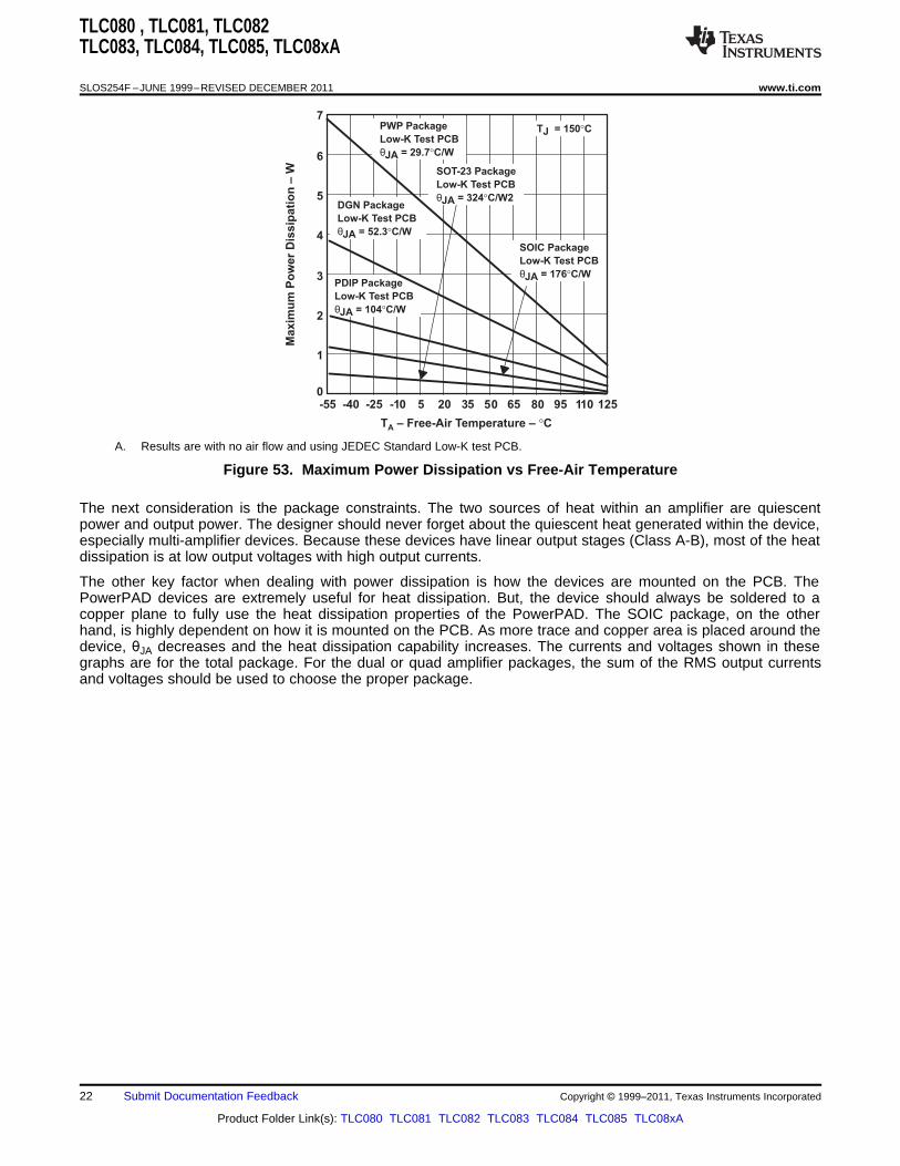
For a given θJA, the maximum power dissipation is shown in Figure 53 and is calculated by the following formula:
(1)
Where:
PD = Maximum power dissipation of TLC08x IC (watts)
TMAX = Absolute maximum junction temperature (150°C)
TA = Free-ambient air temperature (°C)
θJA = θJC + θCA
θJC = Thermal coefficient from junction to case
θCA = Thermal coefficient from case to ambient air (°C/W)
Copyright © 1999–2011, Texas Instruments Incorporated Submit Documentation Feedback 21
Product Folder Link(s): TLC080 TLC081 TLC082 TLC083 TLC084 TLC085 TLC08xA
TJ = 150°C
4
3
2
0-55 -40 -10 20 35
Maxim
um
Po
wer
Dis
sip
ati
on
–W
5
6
7
65 95 125
1
DGN Package
Low-K Test PCB
θJA = 52.3°C/W
SOT-23 Package
Low-K Test PCB
θJA = 324°C/W2
-25 5 50 80 110
PWP Package
Low-K Test PCB
θJA = 29.7°C/W
SOIC Package
Low-K Test PCB
θJA = 176°C/WPDIP Package
Low-K Test PCB
θJA = 104°C/W
T – Free-Air Temperature – CA °
TLC080 , TLC081, TLC082TLC083, TLC084, TLC085, TLC08xA
SLOS254F –JUNE 1999–REVISED DECEMBER 2011 www.ti.com
A. Results are with no air flow and using JEDEC Standard Low-K test PCB.
Figure 53. Maximum Power Dissipation vs Free-Air Temperature
The next consideration is the package constraints. The two sources of heat within an amplifier are quiescentpower and output power. The designer should never forget about the quiescent heat generated within the device,especially multi-amplifier devices. Because these devices have linear output stages (Class A-B), most of the heatdissipation is at low output voltages with high output currents.
The other key factor when dealing with power dissipation is how the devices are mounted on the PCB. ThePowerPAD devices are extremely useful for heat dissipation. But, the device should always be soldered to acopper plane to fully use the heat dissipation properties of the PowerPAD. The SOIC package, on the otherhand, is highly dependent on how it is mounted on the PCB. As more trace and copper area is placed around thedevice, θJA decreases and the heat dissipation capability increases. The currents and voltages shown in thesegraphs are for the total package. For the dual or quad amplifier packages, the sum of the RMS output currentsand voltages should be used to choose the proper package.
22 Submit Documentation Feedback Copyright © 1999–2011, Texas Instruments Incorporated
Product Folder Link(s): TLC080 TLC081 TLC082 TLC083 TLC084 TLC085 TLC08xA
TLC080 , TLC081, TLC082TLC083, TLC084, TLC085, TLC08xA
www.ti.com SLOS254F –JUNE 1999–REVISED DECEMBER 2011
Macromodel Information
Macromodel information provided was derived using Microsim Parts™, the model generation software used withMicrosim PSpice™. The Boyle macromodel (see (1)) and subcircuit in Figure 54 are generated using the TLC08xtypical electrical and operating characteristics at TA = 25°C. Using this information, output simulations of thefollowing key parameters can be generated to a tolerance of 20% (in most cases):• Maximum positive output voltage swing• Maximum negative output voltage swing• Slew rate• Quiescent power dissipation• Input bias current• Open-loop voltage amplification• Unity-gain frequency• Common-mode rejection ratio• Phase margin• DC output resistance• AC output resistance• Short-circuit output current limit(1) G. R. Boyle, B. M. Cohn, D. O. Pederson, and J. E. Solomon, “Macromodeling of Integrated Circuit Operational Amplifiers,” IEEE
Journal of Solid-State Circuits, SC-9, 353 (1974).
Copyright © 1999–2011, Texas Instruments Incorporated Submit Documentation Feedback 23
Product Folder Link(s): TLC080 TLC081 TLC082 TLC083 TLC084 TLC085 TLC08xA

TLC080 , TLC081, TLC082TLC083, TLC084, TLC085, TLC08xA
SLOS254F –JUNE 1999–REVISED DECEMBER 2011 www.ti.com
Figure 54. Boyle Macromodel and Subcircuit
24 Submit Documentation Feedback Copyright © 1999–2011, Texas Instruments Incorporated
Product Folder Link(s): TLC080 TLC081 TLC082 TLC083 TLC084 TLC085 TLC08xA

TLC080 , TLC081, TLC082TLC083, TLC084, TLC085, TLC08xA
www.ti.com SLOS254F –JUNE 1999–REVISED DECEMBER 2011
REVISION HISTORY
NOTE: Page numbers for previous revisions may differ from page numbers in the current version.
Changes from Revision E (April 2006) to Revision F Page
• Updated Figure 9 ................................................................................................................................................................ 10
Copyright © 1999–2011, Texas Instruments Incorporated Submit Documentation Feedback 25
Product Folder Link(s): TLC080 TLC081 TLC082 TLC083 TLC084 TLC085 TLC08xA
PACKAGE OPTION ADDENDUM
www.ti.com 17-Mar-2017
Addendum-Page 1
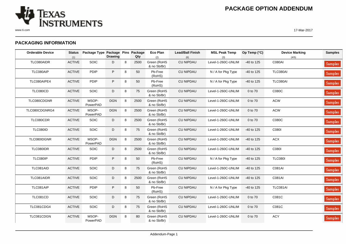
PACKAGING INFORMATION
Orderable Device Status(1)
Package Type PackageDrawing
Pins PackageQty
Eco Plan(2)
Lead/Ball Finish(6)
MSL Peak Temp(3)
Op Temp (°C) Device Marking(4/5)
Samples
TLC080AIDR ACTIVE SOIC D 8 2500 Green (RoHS& no Sb/Br)
CU NIPDAU Level-1-260C-UNLIM -40 to 125 C080AI
TLC080AIP ACTIVE PDIP P 8 50 Pb-Free(RoHS)
CU NIPDAU N / A for Pkg Type -40 to 125 TLC080AI
TLC080AIPE4 ACTIVE PDIP P 8 50 Pb-Free(RoHS)
CU NIPDAU N / A for Pkg Type -40 to 125 TLC080AI
TLC080CD ACTIVE SOIC D 8 75 Green (RoHS& no Sb/Br)
CU NIPDAU Level-1-260C-UNLIM 0 to 70 C080C
TLC080CDGNR ACTIVE MSOP-PowerPAD
DGN 8 2500 Green (RoHS& no Sb/Br)
CU NIPDAU Level-1-260C-UNLIM 0 to 70 ACW
TLC080CDGNRG4 ACTIVE MSOP-PowerPAD
DGN 8 2500 Green (RoHS& no Sb/Br)
CU NIPDAU Level-1-260C-UNLIM 0 to 70 ACW
TLC080CDR ACTIVE SOIC D 8 2500 Green (RoHS& no Sb/Br)
CU NIPDAU Level-1-260C-UNLIM 0 to 70 C080C
TLC080ID ACTIVE SOIC D 8 75 Green (RoHS& no Sb/Br)
CU NIPDAU Level-1-260C-UNLIM -40 to 125 C080I
TLC080IDGNR ACTIVE MSOP-PowerPAD
DGN 8 2500 Green (RoHS& no Sb/Br)
CU NIPDAU Level-1-260C-UNLIM -40 to 125 ACX
TLC080IDR ACTIVE SOIC D 8 2500 Green (RoHS& no Sb/Br)
CU NIPDAU Level-1-260C-UNLIM -40 to 125 C080I
TLC080IP ACTIVE PDIP P 8 50 Pb-Free(RoHS)
CU NIPDAU N / A for Pkg Type -40 to 125 TLC080I
TLC081AID ACTIVE SOIC D 8 75 Green (RoHS& no Sb/Br)
CU NIPDAU Level-1-260C-UNLIM -40 to 125 C081AI
TLC081AIDR ACTIVE SOIC D 8 2500 Green (RoHS& no Sb/Br)
CU NIPDAU Level-1-260C-UNLIM -40 to 125 C081AI
TLC081AIP ACTIVE PDIP P 8 50 Pb-Free(RoHS)
CU NIPDAU N / A for Pkg Type -40 to 125 TLC081AI
TLC081CD ACTIVE SOIC D 8 75 Green (RoHS& no Sb/Br)
CU NIPDAU Level-1-260C-UNLIM 0 to 70 C081C
TLC081CDG4 ACTIVE SOIC D 8 75 Green (RoHS& no Sb/Br)
CU NIPDAU Level-1-260C-UNLIM 0 to 70 C081C
TLC081CDGN ACTIVE MSOP-PowerPAD
DGN 8 80 Green (RoHS& no Sb/Br)
CU NIPDAU Level-1-260C-UNLIM 0 to 70 ACY
PACKAGE OPTION ADDENDUM
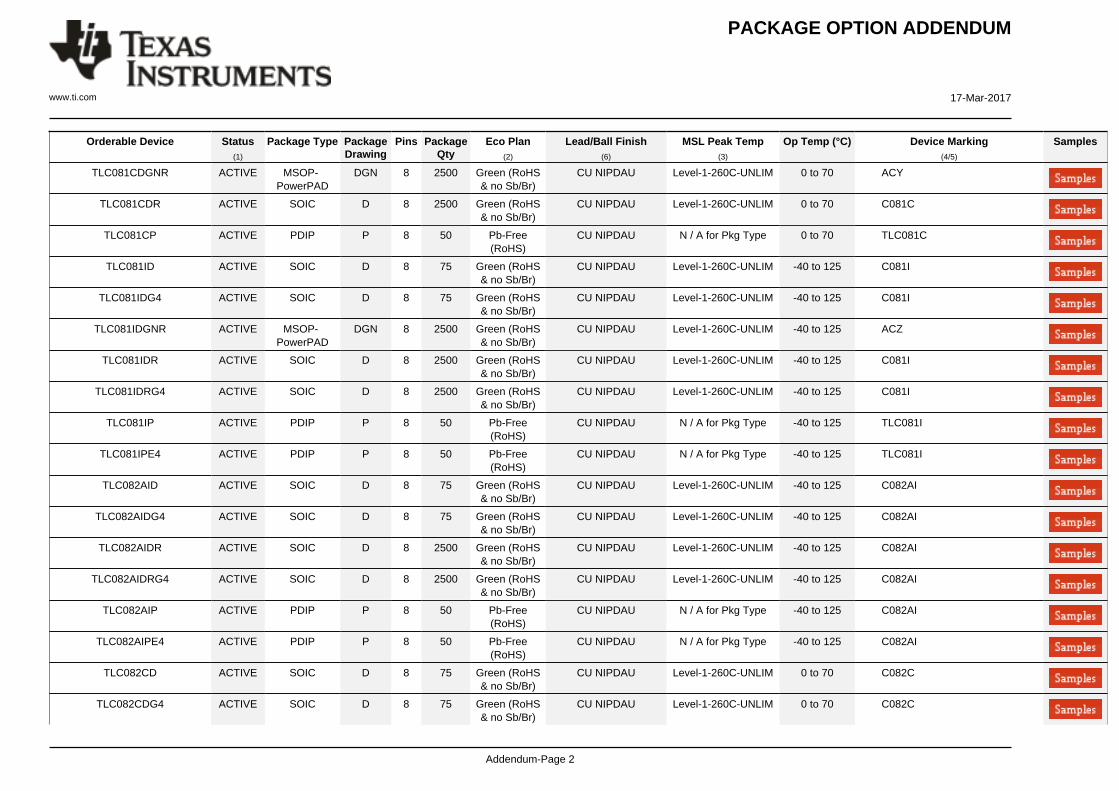
www.ti.com 17-Mar-2017
Addendum-Page 2
Orderable Device Status(1)
Package Type PackageDrawing
Pins PackageQty
Eco Plan(2)
Lead/Ball Finish(6)
MSL Peak Temp(3)
Op Temp (°C) Device Marking(4/5)
Samples
TLC081CDGNR ACTIVE MSOP-PowerPAD
DGN 8 2500 Green (RoHS& no Sb/Br)
CU NIPDAU Level-1-260C-UNLIM 0 to 70 ACY
TLC081CDR ACTIVE SOIC D 8 2500 Green (RoHS& no Sb/Br)
CU NIPDAU Level-1-260C-UNLIM 0 to 70 C081C
TLC081CP ACTIVE PDIP P 8 50 Pb-Free(RoHS)
CU NIPDAU N / A for Pkg Type 0 to 70 TLC081C
TLC081ID ACTIVE SOIC D 8 75 Green (RoHS& no Sb/Br)
CU NIPDAU Level-1-260C-UNLIM -40 to 125 C081I
TLC081IDG4 ACTIVE SOIC D 8 75 Green (RoHS& no Sb/Br)
CU NIPDAU Level-1-260C-UNLIM -40 to 125 C081I
TLC081IDGNR ACTIVE MSOP-PowerPAD
DGN 8 2500 Green (RoHS& no Sb/Br)
CU NIPDAU Level-1-260C-UNLIM -40 to 125 ACZ
TLC081IDR ACTIVE SOIC D 8 2500 Green (RoHS& no Sb/Br)
CU NIPDAU Level-1-260C-UNLIM -40 to 125 C081I
TLC081IDRG4 ACTIVE SOIC D 8 2500 Green (RoHS& no Sb/Br)
CU NIPDAU Level-1-260C-UNLIM -40 to 125 C081I
TLC081IP ACTIVE PDIP P 8 50 Pb-Free(RoHS)
CU NIPDAU N / A for Pkg Type -40 to 125 TLC081I
TLC081IPE4 ACTIVE PDIP P 8 50 Pb-Free(RoHS)
CU NIPDAU N / A for Pkg Type -40 to 125 TLC081I
TLC082AID ACTIVE SOIC D 8 75 Green (RoHS& no Sb/Br)
CU NIPDAU Level-1-260C-UNLIM -40 to 125 C082AI
TLC082AIDG4 ACTIVE SOIC D 8 75 Green (RoHS& no Sb/Br)
CU NIPDAU Level-1-260C-UNLIM -40 to 125 C082AI
TLC082AIDR ACTIVE SOIC D 8 2500 Green (RoHS& no Sb/Br)
CU NIPDAU Level-1-260C-UNLIM -40 to 125 C082AI
TLC082AIDRG4 ACTIVE SOIC D 8 2500 Green (RoHS& no Sb/Br)
CU NIPDAU Level-1-260C-UNLIM -40 to 125 C082AI
TLC082AIP ACTIVE PDIP P 8 50 Pb-Free(RoHS)
CU NIPDAU N / A for Pkg Type -40 to 125 C082AI
TLC082AIPE4 ACTIVE PDIP P 8 50 Pb-Free(RoHS)
CU NIPDAU N / A for Pkg Type -40 to 125 C082AI
TLC082CD ACTIVE SOIC D 8 75 Green (RoHS& no Sb/Br)
CU NIPDAU Level-1-260C-UNLIM 0 to 70 C082C
TLC082CDG4 ACTIVE SOIC D 8 75 Green (RoHS& no Sb/Br)
CU NIPDAU Level-1-260C-UNLIM 0 to 70 C082C

PACKAGE OPTION ADDENDUM
www.ti.com 17-Mar-2017
Addendum-Page 3
Orderable Device Status(1)
Package Type PackageDrawing
Pins PackageQty
Eco Plan(2)
Lead/Ball Finish(6)
MSL Peak Temp(3)
Op Temp (°C) Device Marking(4/5)
Samples
TLC082CDGN ACTIVE MSOP-PowerPAD
DGN 8 80 Green (RoHS& no Sb/Br)
CU NIPDAU Level-1-260C-UNLIM 0 to 70 ADZ
TLC082CDGNG4 ACTIVE MSOP-PowerPAD
DGN 8 80 Green (RoHS& no Sb/Br)
CU NIPDAU Level-1-260C-UNLIM 0 to 70 ADZ
TLC082CDGNR ACTIVE MSOP-PowerPAD
DGN 8 2500 Green (RoHS& no Sb/Br)
CU NIPDAU Level-1-260C-UNLIM 0 to 70 ADZ
TLC082CDR ACTIVE SOIC D 8 2500 Green (RoHS& no Sb/Br)
CU NIPDAU Level-1-260C-UNLIM 0 to 70 C082C
TLC082CDRG4 ACTIVE SOIC D 8 2500 Green (RoHS& no Sb/Br)
CU NIPDAU Level-1-260C-UNLIM 0 to 70 C082C
TLC082CP ACTIVE PDIP P 8 50 Pb-Free(RoHS)
CU NIPDAU N / A for Pkg Type 0 to 70 C082C
TLC082ID ACTIVE SOIC D 8 75 Green (RoHS& no Sb/Br)
CU NIPDAU Level-1-260C-UNLIM -40 to 125 C082I
TLC082IDG4 ACTIVE SOIC D 8 75 Green (RoHS& no Sb/Br)
CU NIPDAU Level-1-260C-UNLIM -40 to 125 C082I
TLC082IDGN ACTIVE MSOP-PowerPAD
DGN 8 80 Green (RoHS& no Sb/Br)
CU NIPDAU Level-1-260C-UNLIM -40 to 125 AEA
TLC082IDGNG4 ACTIVE MSOP-PowerPAD
DGN 8 80 Green (RoHS& no Sb/Br)
CU NIPDAU Level-1-260C-UNLIM -40 to 125 AEA
TLC082IDGNR ACTIVE MSOP-PowerPAD
DGN 8 2500 Green (RoHS& no Sb/Br)
CU NIPDAU Level-1-260C-UNLIM -40 to 125 AEA
TLC082IDGNRG4 ACTIVE MSOP-PowerPAD
DGN 8 2500 Green (RoHS& no Sb/Br)
CU NIPDAU Level-1-260C-UNLIM -40 to 125 AEA
TLC082IDR ACTIVE SOIC D 8 2500 Green (RoHS& no Sb/Br)
CU NIPDAU Level-1-260C-UNLIM -40 to 125 C082I
TLC082IDRG4 ACTIVE SOIC D 8 2500 Green (RoHS& no Sb/Br)
CU NIPDAU Level-1-260C-UNLIM -40 to 125 C082I
TLC082IP ACTIVE PDIP P 8 50 Pb-Free(RoHS)
CU NIPDAU N / A for Pkg Type -40 to 125 C082I
TLC082IPE4 ACTIVE PDIP P 8 50 Pb-Free(RoHS)
CU NIPDAU N / A for Pkg Type -40 to 125 C082I
TLC083AID ACTIVE SOIC D 14 50 Green (RoHS& no Sb/Br)
CU NIPDAU Level-1-260C-UNLIM -40 to 125 C083AI
TLC083AIN ACTIVE PDIP N 14 25 Pb-Free(RoHS)
CU NIPDAU N / A for Pkg Type -40 to 125 C083AI

PACKAGE OPTION ADDENDUM
www.ti.com 17-Mar-2017
Addendum-Page 4
Orderable Device Status(1)
Package Type PackageDrawing
Pins PackageQty
Eco Plan(2)
Lead/Ball Finish(6)
MSL Peak Temp(3)
Op Temp (°C) Device Marking(4/5)
Samples
TLC083CDGQR ACTIVE MSOP-PowerPAD
DGQ 10 2500 Green (RoHS& no Sb/Br)
CU NIPDAU Level-1-260C-UNLIM 0 to 70 AEB
TLC083CDR ACTIVE SOIC D 14 2500 Green (RoHS& no Sb/Br)
CU NIPDAU Level-1-260C-UNLIM 0 to 70 C083C
TLC083CN ACTIVE PDIP N 14 25 Pb-Free(RoHS)
CU NIPDAU N / A for Pkg Type 0 to 70 C083C
TLC083IDGQ ACTIVE MSOP-PowerPAD
DGQ 10 80 Green (RoHS& no Sb/Br)
CU NIPDAU Level-1-260C-UNLIM -40 to 125 AEC
TLC083IN ACTIVE PDIP N 14 25 Pb-Free(RoHS)
CU NIPDAU N / A for Pkg Type -40 to 125 C083I
TLC084AID ACTIVE SOIC D 14 50 Green (RoHS& no Sb/Br)
CU NIPDAU Level-1-260C-UNLIM -40 to 125 TLC084AI
TLC084AIDG4 ACTIVE SOIC D 14 50 Green (RoHS& no Sb/Br)
CU NIPDAU Level-1-260C-UNLIM -40 to 125 TLC084AI
TLC084AIDR ACTIVE SOIC D 14 2500 Green (RoHS& no Sb/Br)
CU NIPDAU Level-1-260C-UNLIM -40 to 125 TLC084AI
TLC084AIDRG4 ACTIVE SOIC D 14 2500 Green (RoHS& no Sb/Br)
CU NIPDAU Level-1-260C-UNLIM -40 to 125 TLC084AI
TLC084AIN ACTIVE PDIP N 14 25 Pb-Free(RoHS)
CU NIPDAU N / A for Pkg Type -40 to 125 TLC084AI
TLC084AIPWP ACTIVE HTSSOP PWP 20 70 Green (RoHS& no Sb/Br)
CU NIPDAU Level-2-260C-1 YEAR -40 to 125 TLC084AI
TLC084AIPWPR ACTIVE HTSSOP PWP 20 2000 Green (RoHS& no Sb/Br)
CU NIPDAU Level-2-260C-1 YEAR -40 to 125 TLC084AI
TLC084AIPWPRG4 ACTIVE HTSSOP PWP 20 2000 Green (RoHS& no Sb/Br)
CU NIPDAU Level-2-260C-1 YEAR -40 to 125 TLC084AI
TLC084CD ACTIVE SOIC D 14 50 Green (RoHS& no Sb/Br)
CU NIPDAU Level-1-260C-UNLIM 0 to 70 TLC084C
TLC084CDG4 ACTIVE SOIC D 14 50 Green (RoHS& no Sb/Br)
CU NIPDAU Level-1-260C-UNLIM 0 to 70 TLC084C
TLC084CDR ACTIVE SOIC D 14 2500 Green (RoHS& no Sb/Br)
CU NIPDAU Level-1-260C-UNLIM 0 to 70 TLC084C
TLC084CDRG4 ACTIVE SOIC D 14 2500 Green (RoHS& no Sb/Br)
CU NIPDAU Level-1-260C-UNLIM 0 to 70 TLC084C
TLC084CN ACTIVE PDIP N 14 25 Pb-Free(RoHS)
CU NIPDAU N / A for Pkg Type 0 to 70 TLC084C

PACKAGE OPTION ADDENDUM
www.ti.com 17-Mar-2017
Addendum-Page 5
Orderable Device Status(1)
Package Type PackageDrawing
Pins PackageQty
Eco Plan(2)
Lead/Ball Finish(6)
MSL Peak Temp(3)
Op Temp (°C) Device Marking(4/5)
Samples
TLC084CNE4 ACTIVE PDIP N 14 25 Pb-Free(RoHS)
CU NIPDAU N / A for Pkg Type 0 to 70 TLC084C
TLC084CPWP ACTIVE HTSSOP PWP 20 70 Green (RoHS& no Sb/Br)
CU NIPDAU Level-2-260C-1 YEAR 0 to 70 TLC084C
TLC084CPWPR ACTIVE HTSSOP PWP 20 2000 Green (RoHS& no Sb/Br)
CU NIPDAU Level-2-260C-1 YEAR 0 to 70 TLC084C
TLC084ID ACTIVE SOIC D 14 50 Green (RoHS& no Sb/Br)
CU NIPDAU Level-1-260C-UNLIM -40 to 125 TLC084I
TLC084IDG4 ACTIVE SOIC D 14 50 Green (RoHS& no Sb/Br)
CU NIPDAU Level-1-260C-UNLIM -40 to 125 TLC084I
TLC084IDR ACTIVE SOIC D 14 2500 Green (RoHS& no Sb/Br)
CU NIPDAU Level-1-260C-UNLIM -40 to 125 TLC084I
TLC084IDRG4 ACTIVE SOIC D 14 2500 Green (RoHS& no Sb/Br)
CU NIPDAU Level-1-260C-UNLIM -40 to 125 TLC084I
TLC084IPWP ACTIVE HTSSOP PWP 20 70 Green (RoHS& no Sb/Br)
CU NIPDAU Level-2-260C-1 YEAR -40 to 125 TLC084I
TLC084IPWPR ACTIVE HTSSOP PWP 20 2000 Green (RoHS& no Sb/Br)
CU NIPDAU Level-2-260C-1 YEAR -40 to 125 TLC084I
TLC084IPWPRG4 ACTIVE HTSSOP PWP 20 2000 Green (RoHS& no Sb/Br)
CU NIPDAU Level-2-260C-1 YEAR -40 to 125 TLC084I
TLC085AID ACTIVE SOIC D 16 40 Green (RoHS& no Sb/Br)
CU NIPDAU Level-1-260C-UNLIM -40 to 125 TLC085AI
TLC085AIDR ACTIVE SOIC D 16 2500 Green (RoHS& no Sb/Br)
CU NIPDAU Level-1-260C-UNLIM -40 to 125 TLC085AI
TLC085AIN ACTIVE PDIP N 16 25 Pb-Free(RoHS)
CU NIPDAU N / A for Pkg Type -40 to 125 TLC085AI
TLC085AIPWP ACTIVE HTSSOP PWP 20 70 Green (RoHS& no Sb/Br)
CU NIPDAU Level-2-260C-1 YEAR -40 to 125 TLC085AI
TLC085CN ACTIVE PDIP N 16 25 Pb-Free(RoHS)
CU NIPDAU N / A for Pkg Type 0 to 70 TLC085C
TLC085CPWP ACTIVE HTSSOP PWP 20 70 Green (RoHS& no Sb/Br)
CU NIPDAU Level-2-260C-1 YEAR 0 to 70 TLC085C
(1) The marketing status values are defined as follows:ACTIVE: Product device recommended for new designs.LIFEBUY: TI has announced that the device will be discontinued, and a lifetime-buy period is in effect.NRND: Not recommended for new designs. Device is in production to support existing customers, but TI does not recommend using this part in a new design.

PACKAGE OPTION ADDENDUM
www.ti.com 17-Mar-2017
Addendum-Page 6
PREVIEW: Device has been announced but is not in production. Samples may or may not be available.OBSOLETE: TI has discontinued the production of the device.
(2) Eco Plan - The planned eco-friendly classification: Pb-Free (RoHS), Pb-Free (RoHS Exempt), or Green (RoHS & no Sb/Br) - please check http://www.ti.com/productcontent for the latest availabilityinformation and additional product content details.TBD: The Pb-Free/Green conversion plan has not been defined.Pb-Free (RoHS): TI's terms "Lead-Free" or "Pb-Free" mean semiconductor products that are compatible with the current RoHS requirements for all 6 substances, including the requirement thatlead not exceed 0.1% by weight in homogeneous materials. Where designed to be soldered at high temperatures, TI Pb-Free products are suitable for use in specified lead-free processes.Pb-Free (RoHS Exempt): This component has a RoHS exemption for either 1) lead-based flip-chip solder bumps used between the die and package, or 2) lead-based die adhesive used betweenthe die and leadframe. The component is otherwise considered Pb-Free (RoHS compatible) as defined above.Green (RoHS & no Sb/Br): TI defines "Green" to mean Pb-Free (RoHS compatible), and free of Bromine (Br) and Antimony (Sb) based flame retardants (Br or Sb do not exceed 0.1% by weightin homogeneous material)
(3) MSL, Peak Temp. - The Moisture Sensitivity Level rating according to the JEDEC industry standard classifications, and peak solder temperature.
(4) There may be additional marking, which relates to the logo, the lot trace code information, or the environmental category on the device.
(5) Multiple Device Markings will be inside parentheses. Only one Device Marking contained in parentheses and separated by a "~" will appear on a device. If a line is indented then it is a continuationof the previous line and the two combined represent the entire Device Marking for that device.
(6) Lead/Ball Finish - Orderable Devices may have multiple material finish options. Finish options are separated by a vertical ruled line. Lead/Ball Finish values may wrap to two lines if the finishvalue exceeds the maximum column width.
Important Information and Disclaimer:The information provided on this page represents TI's knowledge and belief as of the date that it is provided. TI bases its knowledge and belief on informationprovided by third parties, and makes no representation or warranty as to the accuracy of such information. Efforts are underway to better integrate information from third parties. TI has taken andcontinues to take reasonable steps to provide representative and accurate information but may not have conducted destructive testing or chemical analysis on incoming materials and chemicals.TI and TI suppliers consider certain information to be proprietary, and thus CAS numbers and other limited information may not be available for release.
In no event shall TI's liability arising out of such information exceed the total purchase price of the TI part(s) at issue in this document sold by TI to Customer on an annual basis.
OTHER QUALIFIED VERSIONS OF TLC082, TLC084 :
• Automotive: TLC082-Q1, TLC084-Q1
NOTE: Qualified Version Definitions:
• Automotive - Q100 devices qualified for high-reliability automotive applications targeting zero defects

TAPE AND REEL INFORMATION
*All dimensions are nominal
Device PackageType
PackageDrawing
Pins SPQ ReelDiameter
(mm)
ReelWidth
W1 (mm)
A0(mm)
B0(mm)
K0(mm)
P1(mm)
W(mm)
Pin1Quadrant
TLC080AIDR SOIC D 8 2500 330.0 12.4 6.4 5.2 2.1 8.0 12.0 Q1
TLC080CDGNR MSOP-Power PAD
DGN 8 2500 330.0 12.4 5.3 3.4 1.4 8.0 12.0 Q1
TLC080CDR SOIC D 8 2500 330.0 12.4 6.4 5.2 2.1 8.0 12.0 Q1
TLC080IDGNR MSOP-Power PAD
DGN 8 2500 330.0 12.4 5.3 3.4 1.4 8.0 12.0 Q1
TLC080IDR SOIC D 8 2500 330.0 12.4 6.4 5.2 2.1 8.0 12.0 Q1
TLC081AIDR SOIC D 8 2500 330.0 12.4 6.4 5.2 2.1 8.0 12.0 Q1
TLC081CDGNR MSOP-Power PAD
DGN 8 2500 330.0 12.4 5.3 3.4 1.4 8.0 12.0 Q1
TLC081CDR SOIC D 8 2500 330.0 12.4 6.4 5.2 2.1 8.0 12.0 Q1
TLC081IDGNR MSOP-Power PAD
DGN 8 2500 330.0 12.4 5.3 3.4 1.4 8.0 12.0 Q1
TLC081IDR SOIC D 8 2500 330.0 12.4 6.4 5.2 2.1 8.0 12.0 Q1
TLC082AIDR SOIC D 8 2500 330.0 12.4 6.4 5.2 2.1 8.0 12.0 Q1
TLC082CDGNR MSOP-Power
DGN 8 2500 330.0 12.4 5.3 3.4 1.4 8.0 12.0 Q1
PACKAGE MATERIALS INFORMATION
www.ti.com 13-Jan-2018
Pack Materials-Page 1

Device PackageType
PackageDrawing
Pins SPQ ReelDiameter
(mm)
ReelWidth
W1 (mm)
A0(mm)
B0(mm)
K0(mm)
P1(mm)
W(mm)
Pin1Quadrant
PAD
TLC082CDR SOIC D 8 2500 330.0 12.4 6.4 5.2 2.1 8.0 12.0 Q1
TLC082IDGNR MSOP-Power PAD
DGN 8 2500 330.0 12.4 5.3 3.4 1.4 8.0 12.0 Q1
TLC082IDR SOIC D 8 2500 330.0 12.4 6.4 5.2 2.1 8.0 12.0 Q1
TLC083CDGQR MSOP-Power PAD
DGQ 10 2500 330.0 12.4 5.3 3.4 1.4 8.0 12.0 Q1
TLC083CDR SOIC D 14 2500 330.0 16.4 6.5 9.0 2.1 8.0 16.0 Q1
TLC084AIDR SOIC D 14 2500 330.0 16.4 6.5 9.0 2.1 8.0 16.0 Q1
TLC084AIPWPR HTSSOP PWP 20 2000 330.0 16.4 6.95 7.1 1.6 8.0 16.0 Q1
TLC084CDR SOIC D 14 2500 330.0 16.4 6.5 9.0 2.1 8.0 16.0 Q1
TLC084CPWPR HTSSOP PWP 20 2000 330.0 16.4 6.95 7.1 1.6 8.0 16.0 Q1
TLC084IDR SOIC D 14 2500 330.0 16.4 6.5 9.0 2.1 8.0 16.0 Q1
TLC084IPWPR HTSSOP PWP 20 2000 330.0 16.4 6.95 7.1 1.6 8.0 16.0 Q1
TLC085AIDR SOIC D 16 2500 330.0 16.4 6.5 10.3 2.1 8.0 16.0 Q1
*All dimensions are nominal
Device Package Type Package Drawing Pins SPQ Length (mm) Width (mm) Height (mm)
TLC080AIDR SOIC D 8 2500 340.5 338.1 20.6
PACKAGE MATERIALS INFORMATION
www.ti.com 13-Jan-2018
Pack Materials-Page 2
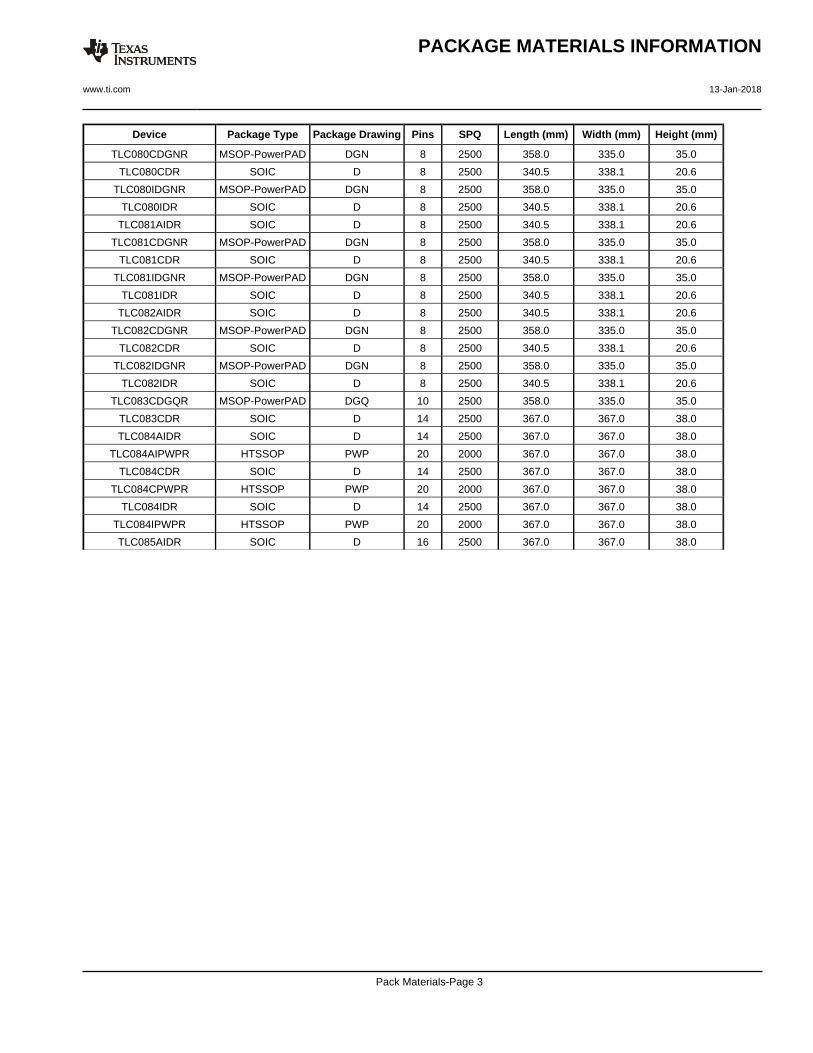
Device Package Type Package Drawing Pins SPQ Length (mm) Width (mm) Height (mm)
TLC080CDGNR MSOP-PowerPAD DGN 8 2500 358.0 335.0 35.0
TLC080CDR SOIC D 8 2500 340.5 338.1 20.6
TLC080IDGNR MSOP-PowerPAD DGN 8 2500 358.0 335.0 35.0
TLC080IDR SOIC D 8 2500 340.5 338.1 20.6
TLC081AIDR SOIC D 8 2500 340.5 338.1 20.6
TLC081CDGNR MSOP-PowerPAD DGN 8 2500 358.0 335.0 35.0
TLC081CDR SOIC D 8 2500 340.5 338.1 20.6
TLC081IDGNR MSOP-PowerPAD DGN 8 2500 358.0 335.0 35.0
TLC081IDR SOIC D 8 2500 340.5 338.1 20.6
TLC082AIDR SOIC D 8 2500 340.5 338.1 20.6
TLC082CDGNR MSOP-PowerPAD DGN 8 2500 358.0 335.0 35.0
TLC082CDR SOIC D 8 2500 340.5 338.1 20.6
TLC082IDGNR MSOP-PowerPAD DGN 8 2500 358.0 335.0 35.0
TLC082IDR SOIC D 8 2500 340.5 338.1 20.6
TLC083CDGQR MSOP-PowerPAD DGQ 10 2500 358.0 335.0 35.0
TLC083CDR SOIC D 14 2500 367.0 367.0 38.0
TLC084AIDR SOIC D 14 2500 367.0 367.0 38.0
TLC084AIPWPR HTSSOP PWP 20 2000 367.0 367.0 38.0
TLC084CDR SOIC D 14 2500 367.0 367.0 38.0
TLC084CPWPR HTSSOP PWP 20 2000 367.0 367.0 38.0
TLC084IDR SOIC D 14 2500 367.0 367.0 38.0
TLC084IPWPR HTSSOP PWP 20 2000 367.0 367.0 38.0
TLC085AIDR SOIC D 16 2500 367.0 367.0 38.0
PACKAGE MATERIALS INFORMATION
www.ti.com 13-Jan-2018
Pack Materials-Page 3
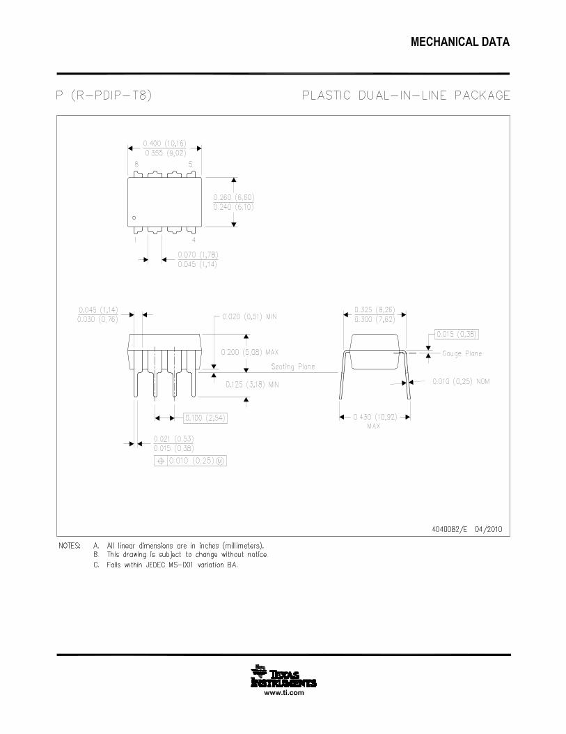
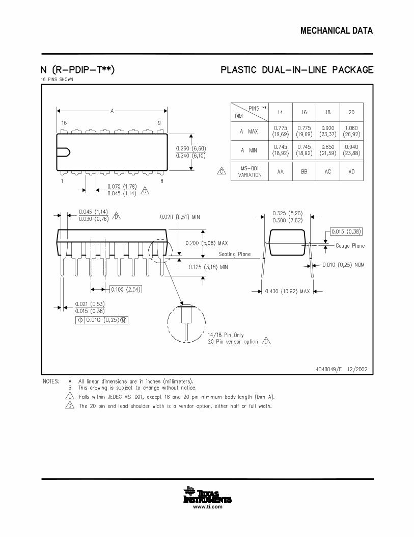


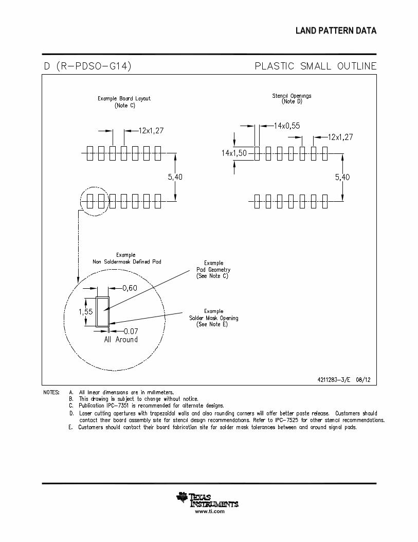
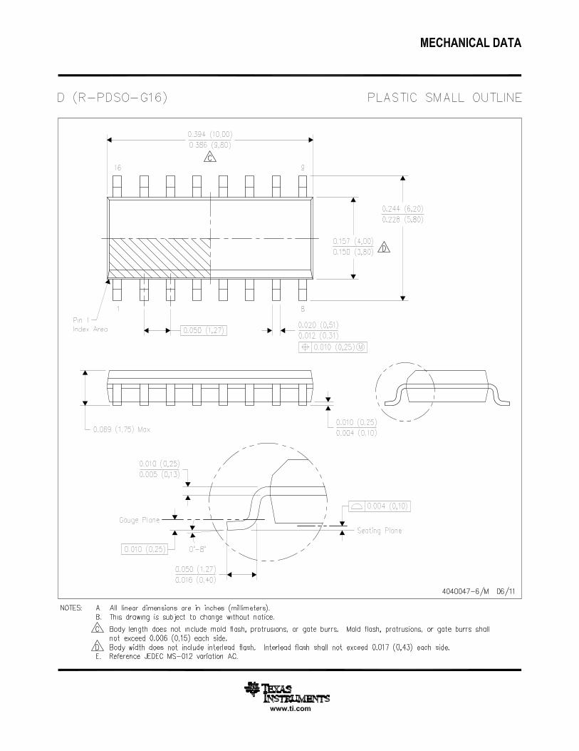
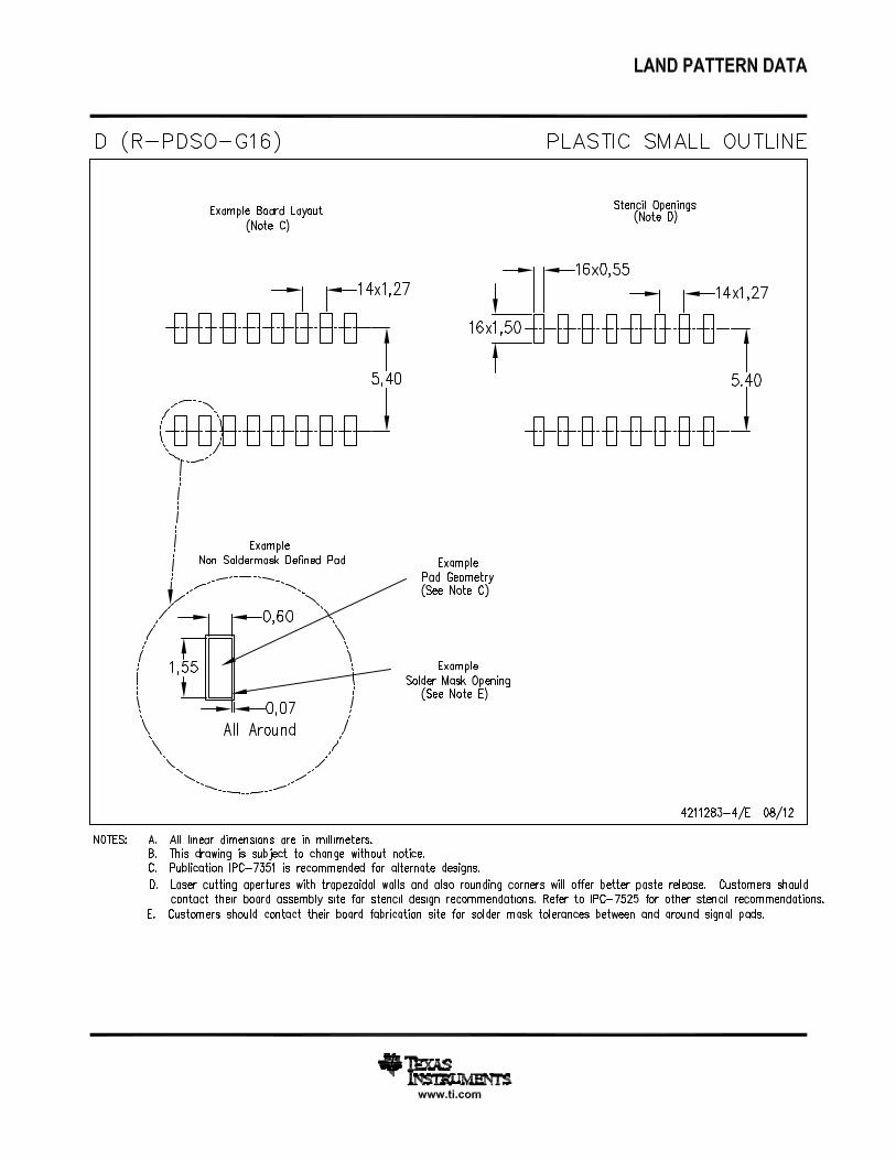
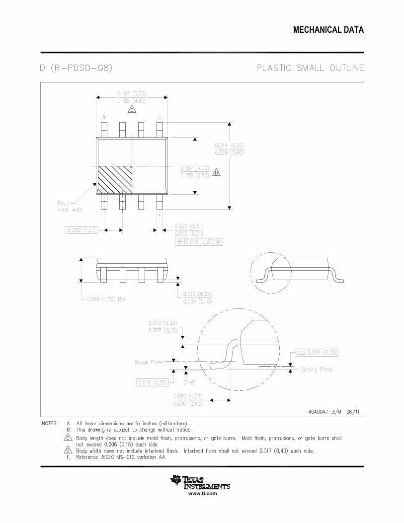


IMPORTANT NOTICE
Texas Instruments Incorporated (TI) reserves the right to make corrections, enhancements, improvements and other changes to itssemiconductor products and services per JESD46, latest issue, and to discontinue any product or service per JESD48, latest issue. Buyersshould obtain the latest relevant information before placing orders and should verify that such information is current and complete.TI’s published terms of sale for semiconductor products (http://www.ti.com/sc/docs/stdterms.htm) apply to the sale of packaged integratedcircuit products that TI has qualified and released to market. Additional terms may apply to the use or sale of other types of TI products andservices.Reproduction of significant portions of TI information in TI data sheets is permissible only if reproduction is without alteration and isaccompanied by all associated warranties, conditions, limitations, and notices. TI is not responsible or liable for such reproduceddocumentation. Information of third parties may be subject to additional restrictions. Resale of TI products or services with statementsdifferent from or beyond the parameters stated by TI for that product or service voids all express and any implied warranties for theassociated TI product or service and is an unfair and deceptive business practice. TI is not responsible or liable for any such statements.Buyers and others who are developing systems that incorporate TI products (collectively, “Designers”) understand and agree that Designersremain responsible for using their independent analysis, evaluation and judgment in designing their applications and that Designers havefull and exclusive responsibility to assure the safety of Designers' applications and compliance of their applications (and of all TI productsused in or for Designers’ applications) with all applicable regulations, laws and other applicable requirements. Designer represents that, withrespect to their applications, Designer has all the necessary expertise to create and implement safeguards that (1) anticipate dangerousconsequences of failures, (2) monitor failures and their consequences, and (3) lessen the likelihood of failures that might cause harm andtake appropriate actions. Designer agrees that prior to using or distributing any applications that include TI products, Designer willthoroughly test such applications and the functionality of such TI products as used in such applications.TI’s provision of technical, application or other design advice, quality characterization, reliability data or other services or information,including, but not limited to, reference designs and materials relating to evaluation modules, (collectively, “TI Resources”) are intended toassist designers who are developing applications that incorporate TI products; by downloading, accessing or using TI Resources in anyway, Designer (individually or, if Designer is acting on behalf of a company, Designer’s company) agrees to use any particular TI Resourcesolely for this purpose and subject to the terms of this Notice.TI’s provision of TI Resources does not expand or otherwise alter TI’s applicable published warranties or warranty disclaimers for TIproducts, and no additional obligations or liabilities arise from TI providing such TI Resources. TI reserves the right to make corrections,enhancements, improvements and other changes to its TI Resources. TI has not conducted any testing other than that specificallydescribed in the published documentation for a particular TI Resource.Designer is authorized to use, copy and modify any individual TI Resource only in connection with the development of applications thatinclude the TI product(s) identified in such TI Resource. NO OTHER LICENSE, EXPRESS OR IMPLIED, BY ESTOPPEL OR OTHERWISETO ANY OTHER TI INTELLECTUAL PROPERTY RIGHT, AND NO LICENSE TO ANY TECHNOLOGY OR INTELLECTUAL PROPERTYRIGHT OF TI OR ANY THIRD PARTY IS GRANTED HEREIN, including but not limited to any patent right, copyright, mask work right, orother intellectual property right relating to any combination, machine, or process in which TI products or services are used. Informationregarding or referencing third-party products or services does not constitute a license to use such products or services, or a warranty orendorsement thereof. Use of TI Resources may require a license from a third party under the patents or other intellectual property of thethird party, or a license from TI under the patents or other intellectual property of TI.TI RESOURCES ARE PROVIDED “AS IS” AND WITH ALL FAULTS. TI DISCLAIMS ALL OTHER WARRANTIES ORREPRESENTATIONS, EXPRESS OR IMPLIED, REGARDING RESOURCES OR USE THEREOF, INCLUDING BUT NOT LIMITED TOACCURACY OR COMPLETENESS, TITLE, ANY EPIDEMIC FAILURE WARRANTY AND ANY IMPLIED WARRANTIES OFMERCHANTABILITY, FITNESS FOR A PARTICULAR PURPOSE, AND NON-INFRINGEMENT OF ANY THIRD PARTY INTELLECTUALPROPERTY RIGHTS. TI SHALL NOT BE LIABLE FOR AND SHALL NOT DEFEND OR INDEMNIFY DESIGNER AGAINST ANY CLAIM,INCLUDING BUT NOT LIMITED TO ANY INFRINGEMENT CLAIM THAT RELATES TO OR IS BASED ON ANY COMBINATION OFPRODUCTS EVEN IF DESCRIBED IN TI RESOURCES OR OTHERWISE. IN NO EVENT SHALL TI BE LIABLE FOR ANY ACTUAL,DIRECT, SPECIAL, COLLATERAL, INDIRECT, PUNITIVE, INCIDENTAL, CONSEQUENTIAL OR EXEMPLARY DAMAGES INCONNECTION WITH OR ARISING OUT OF TI RESOURCES OR USE THEREOF, AND REGARDLESS OF WHETHER TI HAS BEENADVISED OF THE POSSIBILITY OF SUCH DAMAGES.Unless TI has explicitly designated an individual product as meeting the requirements of a particular industry standard (e.g., ISO/TS 16949and ISO 26262), TI is not responsible for any failure to meet such industry standard requirements.Where TI specifically promotes products as facilitating functional safety or as compliant with industry functional safety standards, suchproducts are intended to help enable customers to design and create their own applications that meet applicable functional safety standardsand requirements. Using products in an application does not by itself establish any safety features in the application. Designers mustensure compliance with safety-related requirements and standards applicable to their applications. Designer may not use any TI products inlife-critical medical equipment unless authorized officers of the parties have executed a special contract specifically governing such use.Life-critical medical equipment is medical equipment where failure of such equipment would cause serious bodily injury or death (e.g., lifesupport, pacemakers, defibrillators, heart pumps, neurostimulators, and implantables). Such equipment includes, without limitation, allmedical devices identified by the U.S. Food and Drug Administration as Class III devices and equivalent classifications outside the U.S.TI may expressly designate certain products as completing a particular qualification (e.g., Q100, Military Grade, or Enhanced Product).Designers agree that it has the necessary expertise to select the product with the appropriate qualification designation for their applicationsand that proper product selection is at Designers’ own risk. Designers are solely responsible for compliance with all legal and regulatoryrequirements in connection with such selection.Designer will fully indemnify TI and its representatives against any damages, costs, losses, and/or liabilities arising out of Designer’s non-compliance with the terms and provisions of this Notice.
Mailing Address: Texas Instruments, Post Office Box 655303, Dallas, Texas 75265Copyright © 2018, Texas Instruments Incorporated