
Faculty of Electrical and Electronic Engineering Gerhard ... · Electrical and Electronic...
110
Annual Report 2000 Solid-State Electronics Department Prof.Dr.rer.nat. F.J.Tegude Faculty of Electrical and Electronic Engineering Gerhard-Mercator- Universität Duisburg Fachbereich 9 / Elektrotechnik Halbleitertechnik/Halbleitertechnologie Lotharstrasse 55 / ZHO D-47057 Duisburg Germany Tel.: ++49 (0)203 379 3392 (Secr.) Fax: ++49 (0)203 379 3400 email: [email protected] www: http://www.zho.uni-duisburg.de Editor: Dr.-Ing. Wolfgang Brockerhoff Gerhard - Mercator Universität Duisburg Halbleitertechnik/ Halbleitertechnologie
Transcript of Faculty of Electrical and Electronic Engineering Gerhard ... · Electrical and Electronic...
Annual Report 2000
Solid-State Electronics Department
Prof.Dr.rer.nat. F.J.Tegude
Faculty of
Electrical and Electronic Engineering
Gerhard-Mercator- Universität Duisburg
Fachbereich 9 / Elektrotechnik
Halbleitertechnik/Halbleitertechnologie
Lotharstrasse 55 / ZHO
D-47057 Duisburg
Germany
Tel.: ++49 (0)203 379 3392 (Secr.) Fax: ++49 (0)203 379 3400
email: [email protected]
www: http://www.zho.uni-duisburg.de
Editor: Dr.-Ing. Wolfgang Brockerhoff
Gerhard - MercatorUniversität Duisburg Halbleitertechnik/
Halbleitertechnologie

Annual Report 2000 - Solid-State Electronics Department
Table of Contents
1 Preface ................................................................................................................................. 1
2 Members of the Department ...................................................................................................... 3
3 Teaching Activities .................................................................................................................... 5 3.1 Lectures and Laboratory Exercises ............................................................................................ 5 3.2 Student Reports and Diploma Thesis (Studien-/Diplomarbeiten) ............................................. 8 3.3 Doctor Thesis ............................................................................................................................. 8 3.4 Seminar on Semiconductor Electronics ..................................................................................... 9
4 Research Activities .................................................................................................................. 11 4.1 Materials, Growth and Characterization ............................................................................ 11
4.1.1 Growth and Characterization of InAlP/InGaAs Double Barriers RTDs S.Neumann, P.Velling, M.Haase, A.Osinski, J. Finzel ......................................... 12
4.1.2 LP-MOVPE Growth and Characterization of Ordered InXGa1-XAsy(P1-y) Using Non-Gaseous Sources in N2-Carrier Gas
S. Neumann,. Velling, J. Spieler, T. Kippenberg, Alexandra Lese ....................... 15
4.1.3 High Quality InGaAs/InP HBTs Grown by LP-MOVPE with Non-Gasous Sources
S.Neumann ........................................................................................................... 19
4.1.4 High fT, High Current Gain InP/InGaAs:C HBT Grown by LP-MOVPE with Non-Gaseous Sources
S-O. Kim, P. Velling, M. Agethen ......................................................................... 22
4.1.5 InP-based HBT with graded InGaAlAs Base Layer Grown by LP-MOVPE S-O. Kim, P. Velling, M. Agethen ......................................................................... 25
4.1.6 Characterisation of Interface Effects in Heterostructures by X-ray Rocking Curve Analysis
W. Otten, P. Velling, W. Prost .............................................................................. 28
4.2 Device and Circuit Simulation, Measurement and Modeling .......................................... 31
4.2.1 Two Dimensional Physical Simulation of InP-Heterostructure Bipolar Transistor Using TCAD
B. Schlothmann ..................................................................................................... 32
4.2.2 RF-Noise Modelling of HBT S.Schüller, M.Agethen .......................................................................................... 35
4.2.3 RF-Noise Parameters of HBT in Dependence on Material Parameter S. Schüller, M. Agethen, S. Neumann ................................................................... 38
4.2.4 Cryogenic Temperature Dependence and Modelling of RF-Noise Parameters of InP/InGaAs HBT
M. Agethen, S. Schüller, P. Velling ....................................................................... 41

Annual Report 2000 - Solid-State Electronics Department
4.2.5 Bias Dependent RF-Noise Parameter Modelling of Carbon Doped InP/InGaAs HBT
M. Agethen, S. Schüller, P. Velling ...................................................................... 44
4.2.6. A New Consistent and Scalable PSPICE Model for Enhancement- and Depletion-Type HFET
S. Schüller, R.M. Bertenburg, M. Agethen, A. Brennemann ................................. 47
4.2.7 Magneto Transcondcutance Mobiliy Profiling Carried-Out Using the HP 4145 Parameter Analyser
W. Prost, U. Doerk ............................................................................................... 50
4.2.8 High Frequency Measurement Set-Up for Analog and Digital Circuits in Time Domain
H. van Husen ........................................................................................................ 53
4.2.9 Optical Characterization of Channel Waveguides and Devices M. Yilmaz, M. Swillo, L. Wosinski, W. Brockerhoff ............................................. 56
4.2.10 Development and Implementing of a Test System to Control a Fractional-N-PLL for a Closed Loop Modulation
Th.Kuehn, R.M.Bertenburg .................................................................................. 60
4.2.11 The Development of a Serial Interface for the Connection between Movement Sensors of the Robot and a Controller PC
M. Jürgensen, G. Abba, R. M. Bertenburg ........................................................... 63 4.3 Device and Circuit Processing and Characterization ....................................................... 67
4.3.1 Fabrication of Mushroom Gates in a 2-Layer Resist System Using Electron Beam Lithography
J. Degenhardt ....................................................................................................... 68
4.3.2 Transferred Substrate Technique for InP/InGaAs HBT grown by LP-MOVPE S-O. Kim, P. Velling ............................................................................................. 71
4.3.3 Frequency Dividers Using Gates with Non-linear Negative Feedback A. Brennemann, J. Degenhardt ............................................................................ 74
4.3.4 Design and Layout of RTD/HBT Logic Circuits W. Otten, P. Velling, P. Glösekötter, W. Prost ..................................................... 77
4.3.5 A Depth-2 Full-Adder Circuit using the InP RTD/HFET MOBILE U. Auer, J. Degenhardt, A. Brennemann, W. Prost, C. Pacha ............................. 80
4.3.6 Low-voltage MOBILE Logic Module Based on Si/SiGe Interband Tunnelling Diodes
U. Auer, M. Agethen, W. Prost, R. Duschl, K. Eberl ........................................... 83
4.3.7 Combining HBT and EAM for 1.55µm to a Merged Device T. Reimann, P. Velling, S. Neumann, M. Agethen, R.M. Bertenburg, M. Schneider, R. Heinzelmann, A. Stöhr, M. Haase ............................................ 86

Annual Report 2000 - Solid-State Electronics Department
4.3.8 Laterally Controlled Deposition of Nanoparticles for Microelectronic F. Otten, E.Kruis .................................................................................................. 89
4.4 Conference Contributions ........................................................................................................ 91 4.5 Publications ............................................................................................................................. 94 4.6 12th III/V Semiconductor Devices Simulation Workshop and HBT Workshop...................... 96 4.7 Exhibtion: World on the Wire (Welt am Draht)
R. Glaser, B. Wilken, A. Stöhr, W. Prost ............................................................ 101 4.8 Research Projects .................................................................................................................. 104
5 Guide to the Solid-State Electronics Department ................................................................. 106

Annual Report 2000 - Solid-State Electronics Department 1
1 Preface
This report presents the teaching and research activities of the Solid State Electronics Department (Fachgebiet Halbleitertechnik/Halbleitertechnolgie) during the year 2000. For our Gerhard-Mercator-University as a whole this year was characterized by evaluation and reorganization which tied up a great deal of effort for many of us. Nevertheless, significant progress also has been achieved in our “core business”, teaching and research. Concerning teaching, lectures have been prepared in English, and exercises in III-V-semiconductor technology were conducted for the first time at our department. Students prepare all processing steps necessary to fabricate a hetero-structure-fieldeffect-transistor (HFET).
Research activities are based on three major electronic devices: Heterostructure-FET (HFET), Heterostructure Bipolar Transistor (HBT), and Resonant-Tunnelling-Diode (RTD). But also materials and devices for optoelectronic applications have been prepared, mostly in collaboration with partner groups.
While fundamental HFET work is largely finished and transferred to commercial pilot products, HBT, especially on InP, still suffer from basic problems. So our HFET activities concentrate on design, fabrication and modelling of digital circuits, while the HBT is treated in full span, from MOVPE layer growth with alternative sources and device processing, to rf- and noise characterization as well as simulation and modelling. Special progress has been achieved on RTD/3-terminal devices for digital circuits: Several integrated circuits with RTD/HFET-combinations are realized, including depth-2 full adder circuits. RTD/HBT-elements are fabricated, too, and first elementary gates are realized. For us a new material, we processed Si/SiGe interband tunnelling diodes for the first time.
We were happy to host more than 60 attendees of the 12th III-V Semiconductor Devices Simulation Workshop, this year combined with the HBT Workshop, we organized on October in Duisburg.
Besides research activities we prepared an exhibition of young artists, using our entrance hall, under the motto “World on the Wire”, reflecting a critical dispute with our own work. We particularly appreciate that Uwe Auer, one of my former PhD students, was awarded the best PhD thesis of the Faculty of Electrical and Information Engineering.
Last, but not least, I want to thank all friends and partners for fruitful cooperation and support, and especially all members and students of the department for their efforts and contributions.
Duisburg, March 2001
Prof. Dr.rer.nat. F.J.Tegude

2 Annual Report 2000 - Solid-State Electronics Department
2

Annual Report 2000 - Solid-State Electronics Department 3
2 Members of the Department
head of the department
379- office email
Prof. Dr.rer.nat. Franz-Josef Tegude - 3391 LT 207 [email protected]
secretary
379- office email
Margot Mackenstein (until 4/ 2000)
Dagmar Birke (since 6/2000) - 3392 LT 206 [email protected]
scientific staff
379- office email
Dipl.-Ing. Michael Agethen - 4606 LT 204 [email protected]
Dipl.-Phys. Uwe Auer (until 8/2000) - 3393 LT 105 [email protected]
Dr.-Ing. Ralf M. Bertenburg - 2987 LT 204 [email protected]
Dipl.-Ing. Andreas Brennemann - 2986 LT 104 [email protected]
Dr.-Ing. Wolfgang Brockerhoff (AOR) - 2989 LT 205 [email protected]
Dipl.-Phys. Jan Degenhardt - 3877 LT 104 [email protected]
M. Eng. Seon-Ohk Kim - 4602 LT 106 [email protected]
Dipl.-Phys. Stefan Neumann - 3879 LT 106 [email protected]
Dipl.-Ing. Frank Otten (since 8/2000) - 3393 LT 105 [email protected]
Dr.-Ing. Werner Prost - 4607 LT 205 [email protected]
Dipl.-Phys. Thorsten Reimann - 4605 LT 203 [email protected]
Dipl.-Phys. Holger van Husen - 3394 LT 203 [email protected]
Dipl.-Ing. Peter Velling - 2985 LT 106 [email protected]

4 Annual Report 2000 - Solid-State Electronics Department
technical staff
379- office email
Udo Doerk - 3395 LT 202 [email protected]
Dipl.-Ing. Ralf Geitmann - 4604 LT 202 [email protected]
Dipl.-Ing. Matthias Haase - 4602 LT 106 [email protected]
Dipl.-Ing. Wolfgang Molls - 4603 LT 201 [email protected]
Andrea Osinski - 4600 LT 104 [email protected]
Sabine Schwartz - 4601 LT 105 [email protected]
Ing. (grad.) Reimund Tilders - 3396 LT 201 [email protected]
students
Karsten Bettray Holger Leutfeld
Quoc Thai Do Sascha Mertens
Jörn Driesen Sören Sappok
Jörg Finzel Silja Schüller
Tassilo Gernandt Michael Urlich
Burkhard Heidemann Alexandra Winter
Frank Wittmann
guests
Dr. Dietmar Keiper Royal Institute of Technology, KTH Stockholm, Sweden
Prof.Dr. Landwehr Universität Würzburg, FRG
Alessio Coser Universita di Parma (SOCRATES-program), Parma, Italy
Dr. Thomas Hannappel Hahn-Meitner Institut, Berlin, FRG
Dr. Noren Pan Kopin Corporation, MA, USA
Prof. Dr.rer.nat. M.H.Pillkuhn TU Stuttgart

Annual Report 2000 - Solid-State Electronics Department 5
3 Teaching Activities
3.1 Lectures and Laboratory Exercises
Lectures and exercises Schedule
Solid-State Electronics 1,2 (Festkörperelektronik 1,2)
3rd and 4th semester
Field Effect Electronics (Technische Elektronik 1)
5th semester
Bipolar Transistors and Circuits (Technische Elektronik 2)
6th semester
Semiconductor Microelectronics Technology 1,2 (Halbleitertechnologie 1,2) 7th and 8th semester
Fundamentals of Electronic Devices and Circuits (Grundlagen elektronischer Bauelmente und Schaltungen)
3rd semester / AOS
Basic Electronic Devices and Circuits 6th semester / AOS
III-V Technologies and Components 1/ Semiconductor Technology 1 (Halbleitertechnologie 1)
5th semester
Laboratory exercises
Communication Electronics (Praktikum Technische Elektronik und Hochfrequenztechnik)
7th semester
Introduction to Operational Amplifiers (Operationsverstärker-Praktikum)
6th semester
Semiconductor Technology 2 (Halbleitertechnologie 2)
8th semester
Seminars and Colloquia
Seminar on Semiconductor Electronics (Probleme der modernen Halbleiterphysik)
Seminar on Epitaxial Problems
Colloquium on Optoelectronics (together with other departments)

6 Annual Report 2000 - Solid-State Electronics Department
6
Lectures and Exercises:
Introduction to Solid-State Electronics / Solid-State Electronics 1,2 (Einführung in die Festkörperelektronik) / (Festkörperelektronik 1,2)
These courses start with an introduction to the basics of Quantum physics. Explanations of different atomic-models as well as fundamental physical relations like Schroedinger's equation or uncertainty relation by Heisenberg are given guiding to a comprehensive understanding of semiconductor band structure. The first part (Introduction to Solid-State Electronics) also includes carrier statistics and ends up with a discussion of current continuity and Poisson's equation. In the second part of this lecture the basic building blocks of electronic devices, i.e. semiconductor-metal contact, MIS system, pn junction and heterostructures, are treated for subsequent courses on field effect and bipolar electronics.
Field Effect Electronics (Technische Elektronik 1)
The main topic of this course are the MOS-devices and circuits. Starting with the basics concerning MOS-capacitors and charge-coupled devices, the fundamentals of field-effect transistors (MOSFET, MESFET, JFET) are treated. The basic methods to calculate complex electronic circuits are covered and applied to numerous analog and digital circuits.
Bipolar Transistors and Circuits (Technische Elektronik 2)
This course covers aspects of bipolar devices including an overview about special devices like tunneling and zener diodes. The DC- and AC-behaviour of pn-diodes and bipolar transistors is intensively studied resulting in a discussion of various small-signal equivalent circuits. In the second part complex integrated analog (e.g. operational amplifiers) and digital circuits are analysed and discussed.
Semiconductor Microelectronics Technology 1,2 (Halbleitertechnologie 1,2)
The semiconductor microelectronics technology lectures are devoted to III/V-semiconductor heterostructures for microwave and millimetre wave electronic devices. The process steps from crystal growth to circuit fabrication are discussed. The first semester is focused on heterostructure material issues. Modern growth techniques like molecular beam epitaxy (MBE) and metal-organic vapour-phase epitaxy (MOVPE) are discussed in terms atomic layer control of thickness, composition, and doping. High Resolution X-ray diffraction, photoluminescence, and ellipsometry are explained for non-destructive material assessment in the mono-layer scale. The second semester is devoted to microelectronic fabrication techniques for high speed (f ≥100 GHz) devices and circuits. The lateral and vertical processing of epitaxial films, insulating layers, and metallizations are presented for high performance monolithic millimetre wave integrated circuits.

Annual Report 2000 - Solid-State Electronics Department 7
Laboratory exercises
Communication Electronics (Praktikum Technische Elektronik und Hochfrequenztechnik)
Within the laboratory exercises students apply their theoretical knowledge based on the lectures "Field Effect Electronics" and "Bipolar Transistors and Circuits". The capacitance-voltage charac-teristics of schottky diodes are measured and evaluated. The switching behaviour of bipolar transistors is experimentally investigated as well as the dynamical performance of digital circuits. Additionally, numerical simulation and synthesis of basic electronic circuits are carried out on a UNIX system.
Introduction to Operational Amplifiers (Operationsverstärker-Praktikum)
The aim of this course is the understanding of the basic principles and the characteristics of operational amplifiers (OpAmps). The laboratory exercises demonstrate their applicability in electronic circuits enabling the students to an independent design and understanding of complex circuits. Starting with the measurement and interpretation of the most important characteristic parameters of OpAmps, circuits like adders and multipliers, amplifiers and active filters are intensively calculated and investigated. Oscillators and generators are designed and measured.
Seminars and Colloquia
Seminar on Semiconductor Electronics (Probleme der modernen Halbleiterphysik)
Within this seminar modern topics of the semiconductor electronics are discussed and students, but also members of the department, report about their own work, e.g. the diploma thesis.
Seminar on Epitaxial Problems
Problems of the epitaxial growth of semiconductor structures are analysed, results are interpreted and future trends are discussed.
Colloquium on Optoelectronics Recent developments and problems in the Optoelectronics/Photonics field and neighboured topics are presented by invited experts from all over the world.

8 Annual Report 2000 - Solid-State Electronics Department
3.2 Student Reports and Diploma Thesis
(Studien-/Diplomarbeiten) Student reports
W. OTTEN Röntgendiffraktometrie an Heterostrukturschichten auf InP-Substraten aus der MOVPE
March 2000
S. SCHÜLLER Entwicklung eines SPICE-Modells für InP-Heterostruktur-FET
March 2000
Diploma thesis
M. YILMAZ Optische Charakterisierung von planaren Wellenleitern und Komponenten
January 2000
TH. KUEHN Entwicklung und Inbetriebnahme eines Testsystems zur Ansteuerung einer "Sigma-Delta Fractional-N-PLL" für ein "Closed-Loop"-Modulationsverfahren
August 2000
W. OTTEN Design und Layout von RTD/HBT Logikgattern
Oktober 2000
R.L. MALIK Charakterisierung der spontanen Selbstordnung von InGaAs(P) auf InP
November 2000
S. SCHÜLLER Beiträge zur Hochfrequenz-Rauschmodellierung von HBT
December 2000
B. SCHLOTHMANN Zweidimensionale physikalische Simulation von InP-HBT mit TCAD
December 2000
3.3 Doctor Thesis
W. DAUMANN
Technologie und Charakterisierung von Heterostruktur-Feldeffekttransistoren auf InP-Basis unter Einsatz der Elektronenstrahllithographie
26.06.00
Annual Report 2000 - Solid-State Electronics Department 9
3.4 Seminar on Semiconductor Electronics
17.02.2000 M. JÜRGENSEN, report on the student work:
Entwicklung einer Schnittstellenprogrammierung für die Verbindung zwischen den Bewegungssensoren eines Roboters und dem Steuerechner
MURAT YILMAZ, report on the diploma work: Optische Charakterisierung von planaren Wellenleitern und Komponenten
27.04.2000 S. SCHÜLLER, report on the student work:
Entwicklung eines SPICE-Modells für InP-Heterostruktur-FET
25.05.2000 TH. REIMANN, report on the DFG-project
Wellenleitermodulatoren
08.06.2000 F.-J. TEGUDE, A. BRENNEMANN, report on the conference:
IPRM 2000: 12th Int. Conf. on InP and Related Compounds (14.05.-17.05.2000, Williamsburgh, VA, USA)
15.06.2000 F.-J. TEGUDE, report on the conference:
WOCSDICE 2000: 24th Workshop on Comp. Semicond. Devices and Integrated Circuits (29.05.-02.06.2000, Aegan Sea, Griechenland)
29.06.2000 W. PROST, report on
Schaltungstopologien für RTD/HBT Kombinationen und Anwendungen für digitale Filter
U.AUER, report on the project
Logic Circuits with Reduced Complexity Based on Devices with Higher Functionality
06.07.2000 P. VELLING, report on the conference::
ICMOVPE 2000, Sapporro, Japan, Juni 2000
13.07.2000 M. AGETHEN, report on the conference
Anforderungen und Charakterisierung nichtlinearer Schaltungen" (ITG-Sitzung, München) und "Rauschuntersuchungen an InP-basierenden HBT"
H. VAN HUSEN, report on
Stand und Verbesserung der Hochgeschwindigkeitsdigitalmesstechnik im Fachgebiet HLT
26.10.2000 TH. KÜHN, report on the diploma work:
Entwicklung und Inbetriebnahme eines Testsystems zur Ansteuerung einer "Sigma-Delta Fractional-N-PLL" für ein "Closed-Loop"-Modulationsverfahren

10 Annual Report 2000 - Solid-State Electronics Department
16.11.2000 S.-O.KIM, F.J.TEGUDE, report on the conference:
Europ. GaAs and other Semiconductor Application Symposium ( GAAS 2000), Paris, France, 02.10.00-03.10.00
F.J.TEGUDE, report on the conference:
30th European Microwave Conference, Paris, 02.-05.10.00 A. Brennemann, report on the conference:
Int. Conf. on Union of Radio Science (URSI), Kleinheubach, 25.-29.09.00
30.11.2000 M. PHILIPPENS (RWTH AACHEN), report on the Ph.D.thesis:
Selektive und konforme Abscheidung von (Al)GaAs mittels alternativer chlorhaltiger Metallorganika
07.12.2000 W. OTTEN, report on the diploma work:
Design und Layout von RTD/HBT Logikgattern
14.12.2000 S. SCHÜLLER, report on the diploma work:
Beiträge zur Hochfrequenz-Rauschmodellierung von HBT R.L. MALIK, report on the diploma work:
Charakterisierung der spontanen Selbstordnung von InGaAs(P) auf InP N. PAN, report on the
Reliability of InGaP and AlGaAs HBT, Kopin Corporation, MA, USA

Annual Report 2000 - Solid-State Electronics Department 11
4 Research Activities
4.1 Materials, Growth and Characterization

12 Annual Report 2000 - Solid-State Electronics Department
4.1.1 Growth and Characterization of InAlP/InGaAs Double Barriers RTDs
Scientist: S.Neumann, P.Velling Technical Assistant: M.Haase, A.Osinski Student: J. Finzel
Indroducing
The material system InAlP/InGaAs is of interest especially due to the high conduction band discontinuity at the heterojunction. This material can be used as barrier material for HFET application. A further advantage is the possibility of selective etching of InAlP compared to As containing layers.
In this work we present the first double barrier In0.67Al0.33P/In0.55Ga0.45As/In0.67Al0.33P RTD which is used as a monitor device. The device function is very sensitive to interface effects like roughness, abruptness and homogeneity. However, the growth of this material system is complicated because of the large lattice mismatch of the Al containing material to InP.
A fully non-gaseous source- (ngs-) configuration is used for the growth as described below in detail. The RTD structures are characterized by HRXRD measurements [1], which are compared to simulation results using BEDE Mercury Optimiser software, and dc measurement.
Experimental Setup
All experiments were done on a (001)±0.5 oriented s.i InP:Fe substrate in a low-pressure MOVPE with a horizontal reactor, rf heating and a rotating graphite susceptor (AIX200-System). We use a non-gaseous-source (ngs-) configuration based on TBA and TBP as alternative group V elements, the conventional group III sources TMIn and TEGa and further DitBuSi for n-type doping. With nitrogen as carrier gas we adjust a pressure of ptot=50 mbar and a total flow of Qtot=3.4 slm. The InP layers are grown at Tgr = 600°C ((V/III)InP= 20) while the n+-, nid-InXGa1-XAs and InAlP layers are grown at Tgr= 620°C ((V/III)InGaAs= 5). The n-type doping level of the n+-In0.53Ga0.47As:Si contact layer is determined by van der Pauw Hall measurements to n=1.8.1019cm-3 (µn= 1580 cm2/Vs at 300K) at (IV/III)DitBuSi/TMIn,TEGa= 8%.
The complete device-structure is characterized by high resolution X-ray diffraction with double crystal monochromator and simulated with the commercial program Bede Rads Mercury. The device technology and characterization is done by conventional wet chemical etching procedures and dc-measurements

Annual Report 2000 - Solid-State Electronics Department 13
t= 1.69In0.67Al0.33P
In0.552Ga0.448As
In0.674Al0.326P
t= 5.68 nm
t= 1.69 nm
n+-In0.53Ga0.47As t= 351.4 nm
InP-Substrat, s.i1
2
3
4
6
5
n+-In0.53Ga0.47As t= 148.9 nm
1.8.1019cm-3-1.1016cm-3
1.8.1019cm-3-1.1016cm-3
b)
InAlP/ InGaAs RTD characterization
The layer structures are characterized by HRXRD measurement in the vicinity of the (004)-reflection in a coupled ϖ-2Θ-mode using a double monochromator set-up.
Fig. 1: a) X-Ray characterization result of a strained In0.64Al0.46P/In0.53 Ga0. 47As double barrier RTD. The layer model b) is the result of the simulated rocking curve using BEDE-RADS simulation software.
Figure 1 shows the X-ray measurement and BEDE-RADS simulation of the RTD layer stack, also given in figure 1. The as-grown RTD layer sequence is used for the X-ray simulation and only small variations of about ±10% in composition and thickness of each layer around the intended values are chosen as simulation ranges. An excellent agreement of measured and simulated curve can be achieved with the assumption of ideal interfaces. The Al-content of XAl=33% in the strained InxAl1-xAs barrier layer and the In-content of Xin=56% in the strained InxGa1-xAs well layer is in good agreement with the intended data. The composition of In0.67Al0.33P results in a bandgap of EG,InAlP=2.08 for lattice matched material. The optimiser software is a excellent tool to verify the layers quality, composition and thickness.
∆Θ / arcseconds
101
102
103
104
105
106
-3000 -1000
(400)
simulated
measured
∆ Θ n
1000 3000 50000
log
( in
tens
ity )
/ a.
u.
a)

14 Annual Report 2000 - Solid-State Electronics Department
Measurement and Characterization
Fig. 2 shows the dc-output characteristic of a RTD with an active area of AE=30µm2.
Fig. 2: Output characteristic of a In0.64Al0.46P/In0.53 Ga0. 47As double barrier RTD.
The confinement of electrons in the thin In0.53Ga0.47As-quantum well (W) between the also thin In0.67Al0.33P-barrier layers (B) results in a negative differential resistance regimes (NDR-regime) which were directly correlated to the discrete resonance energy levels existing in the In0.53Ga0.47As-quantum well inside the conduction band.
A very high peak current density of Sp= 3.105 A/cm2 at a VPeak = 1.3 V with an peak to valley current ratio PVR= 1.2 can be achieved. The symmetric behaviour of the dc-measurement shows the high quality of the layerstack and interfaces.
Summary
InAlP/InGaAs structures are grown by LP-MOVPE using a non-gaseous-source configuration with nitrogen carrier gas for the first time. A high peak current density could be achieved. The symmetric behaviour of the output characteristic shows the high material quality . Further investigations are necessary for device application to increase the PVR and to decrease the peak voltage. The RTD structure is useful for X-ray characterisation of the thin strained layers.
References
[1] M. Haase, W. Prost, P. Velling, Q. Liu, F. J. Tegude: "HRXRD for the analysis of ultra thin centre-symmetric strained RTD-heterostructures", Thin Solid Films 319, pp. 25-28, 1998.
T = 300 K, AE=30µm2
S /
105
A/c
m2
UDiode / V-1.5 -1 -0.5 0 0.5 1.5-3
-2
-1
0
1
2
3
bandstructure
EL
EV
E1
(InAl)P - (33% Al, dB= 1.7 nm)
B BW
Barrier (B):
(InGa)As - ( 56% In, dT= 5.6 nm)
NDR-effectWell (W)

Annual Report 2000 - Solid-State Electronics Department 15
ZnSstructure
[010][001]
[100] [111]
CuPtB
structure
4.1.2 LP-MOVPE Growth and Characterization of Ordered InXGa1-XAsy(P1-y) using Non-Gaseous Sources in N2-Carrier Gas
Scientist: S. Neumann, P. Velling, J. Spieler1), T. Kippenberg1) Alexandra Lese1)
1) in collaboration with: Technische Physik I, G. H. Döhler, University Erlangen-Nürnberg
Introduction
The epitaxial growth of ternary and quaternary semiconductor materials, under certain growth conditions [1], yields the spontaneous formation of a superlattice along the [111]B crystal orientations in the form of alternating gallium and indium rich layers along the [111] - and [11 1]- direction (figure 1). The random distribution of the group-III (Indium- and Gallium-) atoms in the zinc-blende- (ZnS-) lattices structure changes to the CuPtB-lattice and the formation of an InAs/GaAs sub lattice is observed.
Fig. 1: Crystal structure of normal (ZnS) and ordered(CuPtB) InGaAs. Ga- and In- rich, monoatomic layers alternate along the [111]B direction.
This symmetry influences the band structure of the crystal and therefore also the electrical and optical characteristics.
Most prominent consequences of the reduced symmetry are a band gap reduction (BGR) and a valence band splitting (VBS) at the Γ point. Optical transitions between the highest valence band and the conduction band are not allowed for light polarized along the [111]B direction. This leads to a strong polarization anisotropy of the optical properties for light propagating perpendicular to the (100) surface.

16 Annual Report 2000 - Solid-State Electronics Department
Further investigation shows spontaneous ordering in the quaternary alloy InGaAsP [2]. By means of electroabsorption measurements (Franz-Keldysh effect FKE) one can obtain very accurate information on a semiconductors band structure as well as on its optoelectronic properties. As both show a significantly anisotropic behaviour for an ordered crystal the experimental results are both of large fundamental interest and extremely useful for polarization dependent optical device applications.
With regard to fibre application it is necessary to use quaternary material. The degree of ordering, described by the odering parameter η, depends on growth parameters like temperature, V/III-ratio and the substrate orientation To achieve the ordering effect, it is necessary to growth at low temperatures. Due to the enhanced cracking efficiency of the metal organic materials TBA, TBP compared to AsH3, PH3 the used ngs-configuration enables growing of quaternary material up to 550°C.
For ordered InGaP [3,4] device applications like polarization sensitive switches [5] or polarization stable light sources [6] have already been demonstrated. A realization in the InGaAs(P)/InP material system seems possible.
Experimental Set-up
The experiments were done on (001) ±0.5° , (001) 2°A and (001) 2°B oriented s.i. InP: Fe epi-ready substrates in an AIX200-system with rf heating at 50mbar reactor pressure using N2 carrier gas and a total gas flow of Qtot = 3.4slm. The ngs-configuration based on TBAs/TBP as group-V the metalorganics TMIn/TEGa/TMAl. A growth temperature range of 500°C < Tgr < 625°C is investigated. The given group-V to group-III ratios (V/III) are calculated from the ratio of the partial pressures of the involved precursors by the assumption of 100% source efficiency. The composition and the quality of the ternary and the quaternary alloys is proven by HRXRD measurements near the 004-reflection in a coupled ω-2Θ-mode using a double monochromator set-up. Further Photoluminescence measurements is used to characterize the layer quality and to specify with HRXRD measurement the composition of the quaternary materials.
Fig. 1: Dependence of the molefraction in the gas phase to achieve lattice matched In0.53Ga0.47As
500 550 600 65040
45
50
55
60
p In
/ (p I
n+ p
Ga)
Tg / °C
InXGa1-XAs, 52% < XIn < 54%

Annual Report 2000 - Solid-State Electronics Department 17
Experimental Results
With the ngs-configuration an N2 carrier gas the growth of InGaAs change above 525°C from the diffusion controlled growth to kinetically controlled growth mode (as can be seen in figure 1).
Above this temperature no modification of the mole fraction in the gas phase is necessary to growth In0.53Ga0.47As lattice matched to InP. With decreasing temperature the mole fraction XGa has to be increased. This is due to the reduced cracking efficiency of the metal organic materials (especially TEGa) at reduced temperatures.
The indium content injected in the gas phase XIn is unchanged during all experiments while for growth temperatures below 525°C the gallium content in the gas phase XGa has to be increased to compensate the reduced cracking efficiency of TEGa.
With polarization dependent electroabsorption measurement (FKE) the BGR can be measurement. These FKE measurements clearly indicate a BGR of up to 40 meV with decreasing growth temperature (figure 3).
Fig. 2: Growth temperature dependent band gap reduction (BGR) for 0.5°, 2°A and 2°B substrates measured with polarization dependent electroabsorption measurements (FKE)
In figure 2 the strong influence of the substrate orientation can be seen. The largest BGR can be observed with 2°B orientated substrate at 525°C. Other substrate orientations show the maximum BGR at higher temperatures. The choice of the substrate orientation and grow temperature enabled a improved band gap engineering.
For most optical devices with regard to fibre application it is necessary to use quaternary material.Figure 3 show the used V/V ratio for lattice matched InGaAsP with a small variation of the composition. With decreasing temperature the TBP partial pressure has to be increased. This is due to the reduced cracking efficiency of TBP at reduced temperature. The composition of the material is calculated from X-ray and PL-measurement. First FKE measurements show a BGR for 550°C and 575°C grown material up to 20 meV.
700
710
720
730
Eg
/ meV
@ 2
0°C
690
0.5°2° [111]A
2° [111]B
Substratorientation:
500 550 600 650Tg / °C

18 Annual Report 2000 - Solid-State Electronics Department
Fig. 3: Dependence of the group V ratio over the growth temperature to achieved lattice matched InxGa1-xAsyP1-y, 65%<xIn<75%, 60%<yAs<70%
Summary
InXGa1-XAsy(P1-y) is grown by LP-MOVPE at reduced temperature which clearly shows ordering. The degree of ordering is studied in dependence of growth temperature and substrate orientation. Similar behaviour which is known from ordered InGaP is found. This material can be used for improved band gap engineering. Further investigations of quaternary material is necessary to determine all growth parameters for lattice matched InGaAsP on InP for 1.3µm and 1.55µm application. First measurements shows a band gap reduction. This enables the material for optical devices in the optical fibre wavelength range.
References:
[1] S. Wei, D. Laks, A. Zunger, APL 62 (16), 1993.
[2] M. A. Shahid and S. Mahajan: „Long-range atomic order in GaxIn1-xAsyP1-y epitaxial layers„, Phys. Rev. B 38(2), 1344 (1988).
[3] Q. Liu, W. Prost, F. J. Tegude, Mat. Sc. and Eng. B 44 (1997), pp 91-95.
[4] Q. Liu, „Characterization of GaInP/GaAs heterostructures by means of x-ray diffractometry and photoluminescence„, Dissertation, Gerhard-Mercator-University-Duisburg, Shaker Verlag 1995.
[5] E. Greger, K. H. Gulden, M. Moser, G. Schmiedel, P. Kiesel, G. H. Döhler, APL 70 (11), 1997.
[6] E. Greger, P. Riel, M. Moser, T. Kippenberg, P. Kiesel, G. H. Döhler, APL 71 (22), 1997.
540 550 560 570 580 590 600 610 620 6300
2
4
6
8
10
12
Tgr [°C]
V/V
rat
io
V/V Gas (pP/pAs)

Annual Report 2000 - Solid-State Electronics Department 19
4.1.3 High Qualitiy InGaAs/InP HBTs Grown By LP-MOVPE With Non Gaseous Sources
Scientist: S. Neumann, P. Velling Student: J. Finzel Technical Assistant: M. Haase, A. Osinski
Introduction
InGaAs/InP HBTs are of pronounced interest for high speed applications. For future commercial application of complex circuits it is necessary to have highly uniform layers. In this work we present stable and robust process based on LP-MOVPE with a non-gaseous-source (ngs-) configuration. HRXRD (high resolution x-ray diffractometer) measurements in the 004- and 002-reflection are compared to simulation results using Bede Rads simulator to estimate the layer quality and homogeneity. In addition, SIMS- and dc-measurement we carried out showing the high quality of the grown layers.
Experimental Set-up
The experiments were done on (001)±0.5° orientated s.i. InP:Fe epi-ready substrates in an AIX200-system with rf-heating at 50mbar reactor pressure using N2 carrier gas and a total gas flow of Qtot= 3.4slm. The ngs-configuration is based on TBAs/TBP/TMAs as group-V, DtBSi/ CBr4 as group-IV dopant sources and the metalorganics TMIn/TEGa/TMAl. A growth temperature range of 500°C < Tg < 620°C and a V/III-ratio range of 0.7 < V/III< 20 are investigated. The group-V to group-III ratios (V/III) and also the group-IV to group-III ratios (IV/III) are calculated from the ratio of the partial pressures of the involved precursors by the assumption of 100% source efficiency. The InP layers are grown at Tg= 600°C ((V/III)InP= 20) while the n+-, nid-InXGa1-xAs layers are grown at Tg= 620°C ((V/III)InGaAs= 5). The n-type doping level of the n+-In0.53Ga0.47As:Si contact layer is determined by van der Pauw Hall measurements to n= 1.8.1019cm-3 (µn= 1580 cm2/Vs at 300K) at (IV/III)DitBuSi/TMIn,TEGa= 8%. A carbon acceptor concentration of p= 1.0.1019m-3 is achieved for p+-In0.53Ga0.47As:C at Tg=500°C (V/III= 0.7). The integrity of the layer structures is proven by HRXRD measurements in the vicinity of the 004 and 002-reflection in a couped Θ-2Θ-mode using a double monochromator setup. The recorded reflection curves are compared to simulations using BEDE RADS Mercury Optimizer software. Device fabrication is done by wet chemical etching and optical lithography.
Results and Discussion
In figure 1 the layer properties are given which were determined automatically by HRXRD measurement and a best fit procedure of the recorded and simulated reflection curve. The intended HBT layer sequence is used for X-ray simulations and only small variation of about ±10% in composition and thickness of each layer around the intended values are chosen as simulation parameters.

20 Annual Report 2000 - Solid-State Electronics Department
Fig.: 1 HRXRD measurement of InGaAs/InP-HBT stucture of the a) (004)-reflection in a coupled Θ-2Θ-mode over 2”-wafer and simulation of the b) (004) reflection with the in c) given layer modell.
The excellent agreement of the measured and simulated rocking curve for the 004-reflex (see fig. 1b) enables the determination of the compostion and thickness (given in c). The period of the fringes can be associated to singel layers of the HBT. The determined values of composition and thickness (layer parameter) is in good agreement with the intended data. The composition of the strained InGaAs base and the nid, n+-InGaAs layers can be determined from the right hand shoulders in figure 1a. It is achieved that the composition of the InGaAs layers varies only in a rangeof ± 0.5% over 2”-wafer.
The SIMS measurement (figure 2) additional show the quality of the HBT. A uniform composition and stabel doping concentration in the Emitter-Cap and the Collector region can be achieved. Further demonstrate the SIMS measurement the very high activation of carbon doping in the base layer of 80%. The low and constant oxygen content in the layers shows the high quality of the used sources. The origin of the high nitrogen content in the base layer is still under discussion. An etching effect caused by CBr4 during the growth of the base layer is assumed to result in the nitrogen incorporation.
-2000 -1000 0 1000 2000
log
( in
tens
ity )
/ a.
u.
0 04 -R e flex
Measured
Simulated
p+-InxGa1-xAs:Cnid-,n+-InxGa1-xAsXIn= 53.2 % ± 0.5 %
M1881
2"-substrat
0 04 -R e flex
XIn= 51.8 % ± 0.5 %
tE-Cap= 135 nm
tE= 67 nm
Theta / arcseconds
a)
b)
c) AnnealingN2 @ 620°C, 2 min.
n+-In0.53Ga0.47As
n-InP
nid-In0.53Ga0.47As
n+-In0.53Ga0.47As
InP
InP, s.i., exact (100)
sub-
CC
BE
subs
trat
eE
-cap
p+-In0.52Ga0.48As:C
tE=67 nm
tE-Cap=135nm
tB=110 nm
tC=293 nm
tSub-C=295 nm

Annual Report 2000 - Solid-State Electronics Department 21
I C, I
B /
A
UBE / V0,2 0,4 0,6 0,8 110-9
10-7
10-5
10-3
10-1
nBE= 1.57 ± 10%
IC
IB
6 - HBT
nBC= 1.16 ± 2%
B @ 105 Acm-2 = 219 ± 4%
2"-Substrat
UCE / V0 0,2 0,4 0,6 0,8 1 1,2 1,60
5
10
15
20
25
30
35
40
IB= 40 µA / Stufe
I C /
mA
AE= 3.15 µm2 (nsa)
M1881
B 200fT= 63 GHz
fmax= 36 GHz
≈ HF-AP
Fig. 2: SIMS measurement confirmed abrupt and high dopant profile for Si- and C-doped InGaAs layers
Figure 3 shows the common emitter output characteristic of one and the gummel-plots of 6 HBT with an active emitter area of 45µm2.
Fig.: 3 Common emitter dc-characteristic and gummel-plot of the InGaAs/InP-HBT
A current gain of B≈200 can be achieved. Futher the devices shows state of the art performance with a extrinsic transit-frequency fT = 68 GHz and maximum frequency of oscillation fmax = 36 GHz. The gummel- plots shows only small variations. This demonstrate again the homogeneity of the grown layers.
Summary
HBT structures are grown by LP-MOVPE using a non-gaseous-source configuration in nitrogen carrier gas. The present results demonstrate the applicability of the ngs-configuation for the growth of highly homogeneously HBTs with state of the art perfomance. Using HRXRD measurement and simulation the layer parameters can be determined and the uniformity can be proofen. SIMS- and dc-measurement confirm these results.
Acknowledgement
The SIMS-measurements are gratefully acknowledged to Noren Pan working (Microlink Devices Inc. / USA). The layers are now commercially avaible by Innovative Processing AG (IPAG).
1016
1017
1018
1019
1020
conc
entr
atio
n /
atom
s/cm
-3
102
103
104
105
106
inte
nsity
/ C
ount
/sec
.
0 0.2 0.4 0.6 0.8 1.0depth / µm
As
GaSiC
H
N
H
O
P
SubstratSub-CCBEE-Cap P
Si

22 Annual Report 2000 - Solid-State Electronics Department
4.1.4 High fT, High Current Gain InP/InGaAs:C HBT Grown by LP-MOVPE with Non-Gaseous Sources
Scientist: S-O. Kim, P. Velling, M. Agethen Introduction
A band-bending effect in the base layer implies an intrinsic electric field which may push minority electrons to the collector. K. Kurishima et al. have presented experimental results showing that HBTs with compositionally graded InGaAs base show a more than 50% improvement in current gain and about 20% in fT compared to a uniform-base structure [1]. Fig 1. shows a comparison of some reported results of fT as a function of dc current gain [2-5]. All high-speed HBT devices (fT 100 GHz) exhibit a limited current gain β ~ 100. This observation is attributed to the need for a low base sheet resistance achieved by a high base doping level (p >> 1019cm-3) which implies low minority life time and hence a low dc current gain [2]. In this work we have adopted the In grading technique using the LP-MOVPE (AIXTRON 200) with non-gaseous source configuration: TBAs and TBP as group-V precursors, TMIn and TEGa as group-III; and DitBuSi/CBr4 for n-/p-type doping. For further improved homogeneity N2 was selected as the carrier gas. Details of growth are given in [6]. In addition, we have used a novel self-aligned B-E-C contact configuration avoiding the emitter/base air-bridge and providing a low access resistance even in the presence of relatively high base sheet resistance (RB > 1000 Ω/ ).
90 100 110 120 130 140 150 160 170
0
100
200
300
400
500
Benchimol: C [2]
Nakajima: Zn[5]
Ito: C[4]Beam: Be[3]
Uni Duisburg
(M1880:C)
Uni Duisburg
(M1883:C)
dc
cu
rre
nt
ga
in
transit frequency (GHz)
Fig. 1: Comparison of dc current gain(β) at high cut off frequency (fT) of some published results ofInP/InGaAs HBTs for different p-type dopant species (C, Be, Zn)
n+-InGaAs (E-Cap) 2x1019 cm-3 135
nm
n-InP (emitter) 5x1017 cm-3 65
nm
p+-InGaAs (base) 1.5x1019 cm-3 70
nm M1880: without
M1883: grading grading
from 53% to 60% In
i-InGaAs (collector) nid. 270
nm
n+-InGaAs (sub-C) 2x1019 cm-3 270
nm

Annual Report 2000 - Solid-State Electronics Department 23
Epitaxial Growth and Device Fabrication
Two samples (M1880 and M1883) are grown with nominally identical epitaxial parameters except for the p-type base layer of sample M1883 with grading of In-component from 53% to 60% (Table 1). The band-diagram of HBT layer stacks with/without In-composition grading is calculated using SimWindows (version 1.5.0) at thermal equilibrium. In Fig. 2 the band-bending is depicted. The calculated potential drop across the graded base is 55mV. Accordingly, the minority carriers are subjected to an electric field towards the collector of 7.9 kV/cm.
HBTs were fabricated using a fast two metalization step processing technology [7] with conventional optical lithography and wet chemical selective etching. The key technology step is the simultaneous and fully self-aligned evaporation of base and collector metalization. The metalic contacts in the active as well as in the pad area are simultaneously evaporated and the separation of active and pad areas is performed by wet chemical underetching realizing a quasi air-bridge configuration. TiAu was evaporated for all contact layers and triple mesa topology was realized using H3PO4:H2O2:H2O solution for InGaAs (emitter-cap, base, collector and subcollector) and HCl:H3PO4 solution for InP (emitter, buffer), respectively. Fig. 3 shows The emitter is oriented parallel to the [010] crystal directions which offer sufficient underetching for self-alignment between emitter and base.
Device Results
In order to prove the homogeneity of the epitaxial layers using non-gaseous sources we have measured gummel plots of six non-self aligned HBTs (M1880, AE=30µm2) from middle to periphery of a 2-inch wafer. The standard deviation of ideality factors nBE and nBC are 1.57±10% and 1.16±2%, respectively (Fig. 4). Based on the results of M1880 we have grown HBT layer stack with a compositionally graded base.
0.1 0.2 0.3 0.4 0.5-1 .4-1 .2-1 .0-0 .8-0 .6-0 .4-0 .20.00.20.40.60.81.01.2
b ase
em itte r
collec tor
En
erg
y (
eV
)
D is tance fro m S urface (µm )
∆Ec=0.055 eV
conventionalbasegraded base
Fig. 2: Calculated energy band diagram of anHBT with conventional (solid line) andcompositionally graded (dashed line) baseat thermal equilibrium.
Fig. 3: SEM picture of the self-aligned HBT contact configuration

24 Annual Report 2000 - Solid-State Electronics Department
The on-wafer S-parameter measurements were performed using an HP8510C network analyzer in the frequency range from 45 MHz to 50 GHz. The non-deembedded cutoff frequency (fT) of 149 GHz is extrapolated (slope of 20 dB/decade) at VCE of 1.5 V and JC=8x10⁴ A/cm2 (Fig. 5). The achieved maximum current gain (βmax) is 400 for this graded base HBT.
The measured maximum current gain and extrapolated cut off frequency of M1880 which has a conventional non-graded base layer are 70 and 125 GHz, respectively, which is still state-of-the-art (cf. Fig. 1).
References
[1] K. Kurishima, H. Nakajima, S. Yamahata, T. Kobayashi, and Y. Matsuoka: Jpn. J. Appl. Phys., Vol. 34 (1995) pp.1221-1227
[2] J.L. Benchimol, J. Mba, A.M. Duchenois, P. Berdaguer, B. Sermage, G. Le Roux, S. Blayac, M. Riet, J. Thuret, C. Gonzalez, and P. Andre: Proc. Of the 11th Int. Conf. on InP and Related Materials, Davos, May 1999
[3] E.A. Beam III, H.F. Chau, T.S. Henderson, W. Liu and A.C. Seabaugh: J. of Crystal Growth 136, 1994.
[4] Kenji Kurishima, Shoji Yamahata, Hiroki Nakajima, Hiroshi Ito and Yasunobu Ishii: Jpn. J. Appl. Phys. Vol 37, 1998, pp. 1353-1358
[5] Hiroki Nakajima, Kenji Kurishima, Shoji Yamahata, Takashi Kobayashi, and Yutaka Matsuoka: Solid-State Electronics Vol. 39, No. 4, 1996, pp. 439-444
[6] P. Velling, M. Agethen, W. Prost, W. Stolz*, F.-J. Tegude: Progress in Crystal Growth and Characterization of Materials (invited), submitted 1.2000.
[7] U. Auer, S-O. Kim, M. Agethen, P. Velling, W. Prost, and F.-J. Tegude: Electronics Letters., Vol. 34, No. 19, 1998, pp. 1885-1886
0
10
20
30
40
50
60
~20 dB/dec
AE=20µm
2
self-aligned
101010.1
M1883
M1880
h2
1 (
dB
)
frequency (GHz)
Fig. 5: The measured cut off frequency of two samples. The Extrapolated fT are 149 GHz (M1883) and 125 GHz (M1880), respectively.
I C, I
B /
A
VBE / V0.2 0.4 0.6 0.8 1
10-9
10-8
10-7
10-6
10-5
10-4
10-3
10-2
10-1
nBE= 1.57 ± 10%
IC
IB
6 - HBT
nBC= 1.16 ± 2%
B@105Acm-2 = 219 ± 4%
2"-Wafer
Fig. 4. The homogeneity of six measuredgummel plots (M1880, AE = 30µm2, nsa).

Annual Report 2000 - Solid-State Electronics Department 25
4.1.5 InP-Based HBT with Graded InGaAlAs Base Layer Grown by LP-MOVPE
Scientist: S-O. Kim, P. Velling, M. Agethen Introduction
For high frequency performance of the Heterojunction Bipolar Transistor (HBT), it is desired to raise the p-doping level in the base layer in order to reduce contact and sheet resistance. Due to the low diffusivity carbon is preferred as an alternative p-dopant over Zn and Be. However, the active hole concentration in carbon-doped InGaAs layer grown by MOVPE in device quality is limited to about 1-2 ⋅1019 cm-3 at 500 °C growth temperature [1]. A higher doping level could be achieved by lowering the growth temperature but material quality and electrical activity will be degraded [2]. Schneider et al. presented experimental results that the hole concentration can be significantly increased by adding Al in InGaAs layer [3]. The presence of Al enforces the incorporation of carbon on group-V lattice sites resulting in higher doping level. Recently, a device demonstration of an InGaAlAs base layer (NA = 1⋅1019 cm-3) in an HBT is reported [4]. Kurishima et al. have presented experimental results that HBTs with compositionally graded InGaAs base show a more than 50% improvement in current gain and about 20% in fT compared to a uniform-base structure [5].
In this work we apply the approach of an InGaAlAs graded base in order to combine high p-type doping and a built-in field in the base. MOVPE growth is performed with non-gaseous source (ngs) configuration using nitrogen carrier gas and TBAs, TBP, and DitBuSi as replacement for the standard precursors AsH3, PH3, and Si2H6/SiH4 [6]. The In-composition in p+-InGaAlAs layer is linearly graded from 60% at the base-collector side to 53% at the base-emitter side. This base-grading results in a intrinsic electric field of 5.4 kV/cm (calculated) for 70 nm layer. Using HR-XRD and photoluminescence measurement we have estimated an Al-content of about 6% in InGaAlAs base layer and the band-gap energy is about 0.815 eV at room temperature. The first demonstrator is fabricated using conventional optical lithography and wet chemical selective etching.
Device Results and Discussion
The Hall measurements showed a increase of maximum hole concentration from 1.5⋅1019 to 3.8⋅1019 cm-3 at Tg = 500 °C for the p+-InGaAlAs:C base layer (µp = 37 cm2/Vs at 300K, Rsh = 730 Ω/). The emitter (InP, Eg ~ 1.35 eV) – base (InGaAlAs, Eg ~ 0.815) junction has a smaller energy difference of about 0.54 eV rather than 0.6 eV of the conventional InGaAs (Eg ~ 0.75 eV) base HBT. Owing to the simulation we have calculated the conduction band discontinuity (∆EC) and valence band discontinuity (∆EV) of 0.225 eV and 0.315 eV, respectively at the emitter-base junction. The base-collector junction also builds a heterojunction and the energy difference is about 0.065 eV without consideration of the bandgap grading.

26 Annual Report 2000 - Solid-State Electronics Department
Table 1: The comparison of the electrical data of InGaAlAs base HBT with InP/InGaAs HBT
Sample (base layer)
NA (cm-3)
Rsheet (Ω/)
ρC (Ωcm2)
VCE,offse
t
(mV)
βmax nB nC BVCEO @ IC = 100 µA
1977 (InxGa1-xAs:
x = 0.53 – 0.60)
1.5⋅1019
1700
8 E-6
200
230
1.73
1.25
3.8 V
1983 (InxGa1-xAl0.06As: x = 0.53 – 0.60)
3.8⋅1019
730
6 E-6
150
35
1.57
1.37
6.3 V
To characterize the InGaAlAs base HBT (sample M1983) we have compared it with InGaAs base HBT (M1977). Both samples have nominal identical layer stacks with same grading condition and growth parameters except the Al-content of the sample M1983. The measured electrical data of the both samples are summarized in table 1. The given doping levels are measured after HBT-fabrication by Van der Pauw Hall measurements and the sheet-/contact resistances are decuced from TLM-measurements at the base layer. A strong decrease in sheet resistance is obtained due to the higher doping level for the sample M1983 but only a slight decrease in contact resistance is achieved which is attributed to the increasing band-gap for the p-InGaAlAs:C base layer. The reduction of dc-current gain from 230 to 35 is attributed to the higher doping level and the increasing alloy scattering in the quaternary base layer. Additionally the valence band discontinuity is reduced by adding Al from about ∆EV ~ 0.348 eV (InGaAs-base, M1977) to ∆EV ~ 0.315 eV (InGaAlAs-base, M1983). Although the value of 35 is still much higher than in other works [e.g. 7], this current gain drop is stronger than our expectation. It is therefore necessary to investigate the characteristics of the Al-content quarternary material in more detail.
Fig. 2: The Gummel plots of the fabricated InP/InGa(Al)As HBT (VBC = 0). See table 2 for ideality factors.
Fig. 1: The common emitter output characteristics of the fabricated HBT with compositionally graded InGaAlAs and InGaAs base layer. Note that the base currents for each sample are different. (IB,InGaAlAs HBT=50 µA/step, IB,InGaAs HBT =10 µA/step)
0.2 0.4 0.6 0.8 1.0 1.21E-10
1E-9
1E-8
1E-7
1E-6
1E-5
1E-4
1E-3
0.01
0.1
1
10
VBC
= 0
InGaAlAs base HBT (M 1983)
InGaAs base HBT (M 1977)
I B,
IC (
A)
VBE
(V )0.0 0.3 0.6 0.9 1.2 1.5
5
15
0
10
20
InGaAlAs base HBT (M1983)
InGaAs base HBT (M1977)
I C (
mA
)
V CE (V)

Annual Report 2000 - Solid-State Electronics Department 27
Figure 1 shows the common emitter output characteristics of both samples. Note that the base current for each sample is different. As expected the offset voltage of the sample M1983 is a little bit smaller than M1977 due to the smaller band-gap difference of the e-b and b-c diodes (about 60 meV). The measured Gummel plots (fig. 2) also show the smaller turn-on voltage of the sample M1983 in the low VBE regime. Another fact in addition is the output conductance of the sample M1983 is very low resulting in a high Early voltage. The measured breakdown voltage of the sample M1983 at IC = 100 µA (IB = 0) is 6.3 V and much higher than 3.8 V of the sample M1977.
The on-wafer S-parameter measurements were performed using an HP8510C network analyzer in the frequency range from 45 MHz to 40 GHz. The non-deembedded cutoff frequency (fT) of 117 GHz and maximum oscillation frequency (fmax) of 90 GHz are extrapolated (slope of 20 dB/decade) at VCE of 2.0 V and JC=8x10⁴ A/cm2.
References
[1] D. Keiper, R. Westphalen, G. Landgren
„Comparison of carbon-doping of InGaAs and GaAs by CBr4 using hydrogen or nitrogen as carrier-gas in LP-MOVPE”, J. Crystal Growth 197 (1999) 25-30
[2] D. Keiper, P. Velling, W. Prost, M. Agethen, F.J. Tegude, G. Landgren
„Metalorganic Vapour Phase Epitaxy (MOVPE) Growth of InP-based Heterojunction Bipolar Transistors (HBT) with Carbon Doped InGaAs Base Using tertiarybutylarsine (TBA), tertiarybutylphosphine (TBP) in N2 Ambient“, Jpn. J. App. Phys. 39, (2000) pp. 6162-6165
[3] J. M. Schneider, K. Bitzer, J. Rieger, H. Heinecke
„Highly carbon-doped GaInAs contact layers grown by using carbontetrabromide in MBE on MOVPE 1.55 µm GaInAsP/InP MQW laser structures”, J. Crystal Growth 188 (1998) pp. 56-62
[4] W. C. Liu, H.J. Pan, S.Y. Cheng, W.C. Wang, J.Y Chen, S.C. Feng, K.H. Yu
“Applications of an InGaAlAs/InP continuous-conduction-band structure for ultralow current operation transistors”, Appl. Phys. Lett. 75 (1999) pp. 572-574
[5] K. Kurishima, H. Nakajima, S. Yamahata, T. Kobayashi, Y. Matsuoka
“Effects of a Compositionally-Graded InGaAs Base in Abrupt-Emitter InP/InGaAs HBTs”, Jpn. J. Appl. Phys., Vol. 34 (1995) pp.1221-1227
[6] P. Velling, M. Agethen, W. Prost, W. Stolz, F.-J. Tegude
“A comparative study of GaAs- and InP-based HBT growth by means of LP-MOVPE using conventional and non gaseous sources”, accepted for Progress in Crystal Growth and Characterization of Materials (invited),
[7] K. Kurishima, S. Yamahata, H. Nakajima, H. Ito, Y. Ishii
“Performance and Stability of MOVPE-Grown Carbon-Doped InP/InGaAs HBT’s Dehydrogented by an Anneal after Emitter Mesa Formation”, Jpn. J. Appl. Phys. Vol. 37 (1998) pp. 1353-1358

28 Annual Report 2000 - Solid-State Electronics Department
4.1.6 Characterisation on Interface-Effects in Heterostructures by X-Ray Rocking Curve Analysis
Student: W. Otten Supervisor: P. Velling, W. Prost
Introduction
The realization of heterostructures with smooth, nearly atomically abrupt and defect-free interfaces is of significance for the device applications. X-ray diffractometry offers the possibility to determine non-destructively several parameters of an epitaxial grown stack with a monolayer resolution. The report will show one way of considering the effects of interlayers in the simulation of X-ray rocking curves.
Motivation
The Scanning Transmission Electron Microscopy shot (STEM, c.f. fig. 1) of an InP/InGaAs epitaxial stack shows the interlayers caused by physical and/or technological origin. Considering the blurred contours corresponding to the fluctuation in the relevant interlayer thickness it would appear that also the composition in the single layer is fluctuating along the heterointerface. The varying shades of grey of both interlayers show that the composition of the interlayer at the InGaAs-to-InP transition is different from that at the InP-to-InGaAs transition. Visible roughness and differences of concentration demand a consideration in the X-ray simulations.
To find a suitable way to consider the interlayers in X-ray simulations InAlAs/InGaAs, InGaAs/InP and InAlAs/InP super-lattices (SL) grown at 620°C/600°C were characterized by high resolution X-ray diffraction (HRXRD) measurements which are compared to simulations using Bede RADS Mercury Simulator. It calculates rocking curves automatically by evaluating statistical parameters for Goodness of Fit and using the fundamental X-ray scattering equations of dynamical diffraction (generic algorithm). Position and intensity of the peaks, their modulation/damping, and their line width (Full Width at Half Maximum height, FWHM) were used to assess the grown structures concerning to the clear outlines, thickness, and composition of the interface. The width of the peaks and their decrease in intensity (damping) at high angular values in the vicinity of the investigated (004)-reflexion is decisively characterized by the nature of the inter-face. That means that roughness and spatially different compositions lead to a widening of the corresponding peaks.
Results
Abrupt interfaces were found for the InAlAs/InGaAs SL (no group-V exchange) while for the InAlAs/InP and InGaAs/InP SL with group-V exchange strained interfacial layers were identified (c.f. fig.2) by X-ray analysis. A maximum agreement between simulation and measurement concerning to modulation and width of the peaks are reached by considering the relaxation-parameter of RADS Mercury.
Annual Report 2000 - Solid-State Electronics Department 29
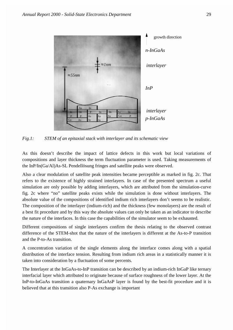
Fig.1: STEM of an epitaxial stack with interlayer and its schematic view
As this doesn’t describe the impact of lattice defects in this work but local variations of compositions and layer thickness the term fluctuation parameter is used. Taking measurements of the InP/In(Ga/Al)As-SL Pendellösung fringes and satellite peaks were observed.
Also a clear modulation of satellite peak intensities became perceptible as marked in fig. 2c. That refers to the existence of highly strained interlayers. In case of the presented spectrum a useful simulation are only possible by adding interlayers, which are attributed from the simulation-curve fig. 2c where “no” satellite peaks exists while the simulation is done without interlayers. The absolute value of the compositions of identified indium rich interlayers don’t seems to be realistic. The composition of the interlayer (indium-rich) and the thickness (few monolayers) are the result of a best fit procedure and by this way the absolute values can only be taken as an indicator to describe the nature of the interfaces. In this case the capabilities of the simulator seem to be exhausted.
Different compositions of single interlayers confirm the thesis relating to the observed contrast difference of the STEM-shot that the nature of the interlayers is different at the As-to-P transition and the P-to-As transition.
A concentration variation of the single elements along the interface comes along with a spatial distribution of the interface tension. Resulting from indium rich areas in a statistically manner it is taken into consideration by a fluctuation of some percents.
The Interlayer at the InGaAs-to-InP transition can be described by an indium-rich InGaP like ternary interfacial layer which attributed to originate because of surface roughness of the lower layer. At the InP-to-InGaAs transition a quaternary InGaAsP layer is found by the best-fit procedure and it is believed that at this transition also P-As exchange is important
PAsIn
AsIn
AsP
As
PAs
InIn In InInP
InAs
Ga
Ga
growth direction
n-InGaAs
interlayer
InP
interlayer
p-InGaAs
1nm
55nm
≈
≈

30 Annual Report 2000 - Solid-State Electronics Department
.
Summary:
An X-ray diffraction of an SL without group-V-exchange shows satisfying agreements between X-ray-analysis and simulation also without interlayers. But super-lattices with group-V-exchange demonstrate, that thin, highly strained, indium rich interlayers and a fluctuation-parameter have to be taken into consideration. By that way variations of compositions and thicknesses in epitaxial stacks can be considered, and satisfying agreements can be made between measured and simulated rocking curves. The in this work identified interface-characteristics are now taken into account for the X-ray analysis of more complex heterostructure-bipolar-transistor (HBT) and heterostructure-field-effect-transistor (HFET) device structures.
References:
[1] Software: „Rads Mercury v3.50c“, Bede Scientific Instruments Ltd.
[2] V.S. Speriosu und T. Vreeland: "X-ray rocking curve analysis of superlattices", J. Appl. Phys. 56(6),1591-1600 (1984).
[3] Q. Liu: "Characterization of GaInP/GaAs and GaInP/InP heterostructures by means of x-ray diffractometry and photoluminescence", Dissertation, Gerhard-Mercator-Universität Gesamthochschule Duisburg, 1995.
s i m u l a t i o n d a t a ( b e s t 1 0 - p e r i o d S L t / nm In Ga As P 0.9
InP (V/III=20) 10.7
In0.73Ga0.27As0.02P0.98 0.3
In0.53Ga0.47As (V/III=5) 27.6
InP-Buffer (V/III=20) 57.4
InP-Substrate Tgr=600oC
Tab.1: InGaAs/InP layer stack
grown by LP-MOVPE as best fit simulation with interlayers
-4,000 -3,000 -2,000 -1,000 0 1,000 2,000 3,000
log
(In
ten
sit
y)
/ a
.u.
( 0 0 4 )
∆ Θ / a r c s e c
a)
b)
c)
satelite peakmodulation
0
+1
+2+3 +4
-1
-2
-4-5-3
Fig.2: x-ray diffraction patterns of InGaAs/InP SL
inthe vicinity of the (004)-reflexion: a) measured, b) simulated with interlayers
and c) simulated without interlayers

Annual Report 2000 - Solid-State Electronics Department 31
4.2 Device and Circuit Simulation
32 Annual Report 2000 - Solid-State Electronics Department
4.2.1 Two Dimensional Physical Simulation of InP-Heterostructure Bipolartransistor Using TCAD
Scientist: Björn Schlothmann
Introduction
For smaller and more powerful devices, development tools are needed, which describe all relevant effects of the investigated device. First results for InP/InGaAs Heterostructure Bipolartransistors (HBTs) using Technology-Computer-Aided-Design (TCAD) software package by Silvaco will be presented. This package has originally been developed for silicon-based technology and devices, but there are additional software modules available which enable real physical simulation of III-V-compound semiconductor based devices and processes. ATHENA, the general physics-based, two dimensional simulator of semiconductor processing is enhanced by FLASH to perform both, analysis and optimisation, of compound semiconductor structures. ATLAS, the general device simulator, is extended by BLAZE to calculate heterostructure devices. Especially for bipolar devices, an additional module is available to consider thermal effects (GIGA), which at least becomes essential for high-power device simulations.
Device Simulation
One major point in the physical device simulation is the mesh definition of the structure. For the simulator a mesh defines the points of calculation inside the structure. It is important to make a sophisticated mesh refinement. A coarse mesh results in large calculation errors or even unphysical results. A very fine mesh reduces the mathematical error, but extents the calculation time drastically. By this means, a trade-off has to be found by applying smart mesh refinement processes.
For reliable results the simulator has to be calibrated (model and material parameters) with measured devices. The initial definition of material parameters is done using values known from literature [1][2]. These values have to be investigated and calibrated with well known device structures. For the first simulation of HBTs we use drift-diffusion-transport model (with its modifications for heterostructures [3]), fermi-dirac statistic (to take into account highly doped regions), negative differential mobility model, Shockley-Read-Hall recombination, Auger recombination, direct recom-bination, impact ionisation, and bandgap narrowing.
0.6 0.7 0.8 0.9 1.0 1.1 1.2 1.30
1
2
3
4
5
6
7
8
9
10
UBE (V)
IB (mA)
assumption ofsharp interface
heterojunction withinterface layer:
d= 0.2 nm, 0.4 nm, 1 nm,2 nm, 4 nm, 10 nm
d
d= 10 nm
Fig. 1: Variation of the interface layer thickness.

Annual Report 2000 - Solid-State Electronics Department 33
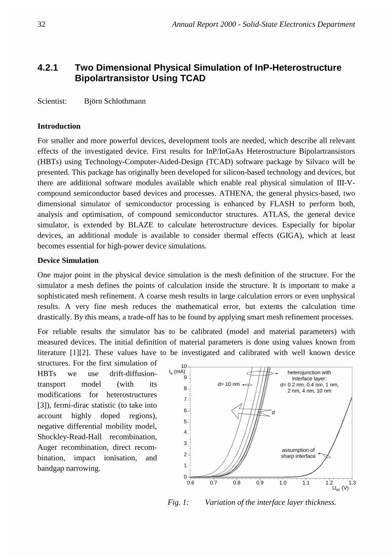
Results
First simulation of the dc-characteristic of the HBT show a high offset of the threshold voltage in the base-emitter-diode (fig.1). After defining an additio-nal interface layer between the InGaAs base and the InP emitter, the threshold voltage decrease by about 0.4 V, a better fit between simulated and measured data is obvious. Fig.2 shows the differences in band diagram of the emitter-base junction with and without interface layer. With this 1nm thick undoped layer, simulations of the dc-characteristics show good agreement between simulated and measured data (fig. 3-6). Further improved models (e.g. surface recombination) will
0.0 0.1 0.2 0.3 0.4 0.5 0.6 0.7 0.8
0
10
20
30
40
50
60
70
1e-15
1e-13
1e-11
1e-9
1e-7
1e-5
1e-3
1e-1
1e+1
UBC (V)0.9
IB (mA) I B ( A)measurement: n= 1.6simulation: n= 1.7
measurement
measurement
simulation
0.0 0.1 0.2 0.3 0.4 0.5 0.6 0.7 0.8 0.9 1.0
0
2
4
6
8
10
12
14
16
1e-17
1e-15
1e-13
1e-11
1e-9
1e-7
1e-5
1e-3
1e-1
1e+1
UBE (V)
IB (mA)IB (A)
measurement
measurement
simulation
simulation
measurement: n= 1.5simulation: n= 1.6
base-collector diode base-emitter diode
Fig.3 and 4: Comparison of the simulated and measured dc-characteristic of the investigated device.
0 0.2 0.4 0.6 0.8 1.21.0 1.4UCE (V)
0
2
4
6
8
10
12
14
16IC (mA)
I B=
50 m
AI B
= 3
0 m
AI B
= 10
mA
measurementsimulation
IB
IC
measurement
simulation
measurement: nC= 1.6 nB= 1.3
simulation: nC= 1.8 nB= 1.7
0.0 0.1 0.2 0.3 0.4 0.5 0.6 0.7 0.8 0.9 1.01e-10
1e-9
1e-8
1e-7
1e-6
1e-5
1e-4
1e-3
1e-2
1e-1
UBE (V)
IC, IB (A)
Gummel-Plotoutput characteristic
Fig.5 and 6: Measured and simulated dc-characteristic of the investigated device.
n-InP 5*1017 cm-3 - emitter
p-InGaAs 1.5*1019 cm-3 - base
WV WF WC0.2 eV
0.5 nm
n-InP 5*1017 cm-3 - emitter
n-InP 1*1014 cm-3 - emitter ILp-InGaAs 5*1015 cm-3 - base IL
p-InGaAs 1.5*1019 cm-3 - base
heterojunctionwith
interface layer (IL)
abruptheterojunction
Fig.2: Banddiaram and layer-stack of the interface layer.

34 Annual Report 2000 - Solid-State Electronics Department
improve the results.
For the comparison of the measured and simulated rf-data, a technique is developed to generate a parasitic-environment for the simulated data. This is necessary because the simulator calculates the rf-performance of the device in an ideal environment without any parasitics (e.g. pad-capacitances). Therefore, the simulated s-parameters are used as input data for a sub circuit included in a parasitic-environment, which is optimised using Microwave Design System (MDS) by Hewlett-Packard. The optimised values of the equivalent circuit are compared with small signal modelling results. The parasitics are found within the expected range and finally a good agreement can be achieved between simulated and measured s-parameters (fig.7).
Conclusion
With the TCAD environment by Silvaco it is possible to simulate the complex behaviour of the investigated InP/InGaAs HBT. First results show good agreement between simulated measured dc- and rf-data. Further investigations including additional models will lead to improved results.
References:
[1] A. F. Salem et al., “Theoretical Study of Response of InGaAs Metal-Semiconductor-Metal Photodetectors”, IEEE Journal Of Quantum Electronics, Vol. 31, No. 5, May 1995
[2] D. Sawdai et al., “Performance Optimisation of PNP InAlAs/InGaAs HBTs”, 16th Biennial IEEE/Cornell University Conference on Advanced Concepts in High-Speed Semiconductor Devices and Circuits, August 1997
[3] Silvaco International, “User’s Manual”, Santa Clara, 2000
S22
S21
S11
S12
OM
OM
OM
OM1
-1 10 0 1-110
Fig.7: The measured (M) and simulated (O) rf-data (0.5 GHz < f < 40 GHz).

Annual Report 2000 - Solid-State Electronics Department 35
4.2.2 RF-Noise Modelling of HBT
Student: S. Schüller Scientist: M. Agethen Introduction
HBT rf-noise models are often based on the noise circuit theory including only two correlated noise current sources, one at the input taking into account the noise of the base current IB and the other at the output modelling noise effects due to collector current IC. A modelling of all rf-noise parameters (minimum noise figure Fmin, equivalent noise resistance Rn and optimum generator reflection coefficient Γopt) is possible. Up to now, information about intrinsic noise sources is not included and therefore an extended understanding of physical noise phenomena in HBT devices is not possible. Within this work a rf-noise model has been developed, which localise the intrinsic noise sources of the HBT and is able to model s-parameters as well as all rf-noise parameters simultaneously.
The consistent small-signal and rf-noise model
From noise circuit theory it is well known, that in case of narrow band noise a noisy impedance or admittance can be replaced using the one-port noise equivalent circuits given in fig.1. Noisy impedances are modelled including a noise voltage source in series to the impedance, which is then assumed to be noiseless. The effective value of the noise voltage can be calculated using the well known equation given in fig. 1, too. Noisy admittances are modelled in an analogous way (see fig.1b). The model parameter describing the noise of the impedance or admittance is the equivalent noise temperature Tn which is associated to the noisy element. Both equivalent noise circuits of one-ports are now consequently included in complex circuits, here in the well known physically relevant “T”-like small-signal equivalent circuit of HBT. To all resistances equivalent noise temperatures are associated, which describe the noise effect of these elements in the circuit.
Z(f)Tn≠0K
Z(f)T=0K
= uZ,th
a) Impedance form
( ) ( ) fZfTfuZ ℜ= n
2
th, k4 ∆
=Y(f)
Tn≠0KY(f)
T=0KiY,th
b) Admittance form
( ) ( ) fYfTfiY ℜ= n
2
th, k4 ∆
Fig. 1: Noise equivalent circuits of a) noisy impedance and b) noisy admittance. Fig.2 shows the extended small-signal equivalent circuit of HBT, which builds up the basis of the new consistent small-signal and rf-noise parameter model. This “T”-like equivalent circuit can easily be found considering the typical three-mesa design of III-V semiconductor based HBT. In case of narrow band noise, equivalent noise temperatures are associated with all resistances. In fig.2 all equivalent noise temperatures are included.

36 Annual Report 2000 - Solid-State Electronics Department
As usual, the small-signal model is divided into two parts, an intrinsic and an extrinsic one. The extrinsic resistances only add thermal noise, consequently their equivalent noise temperature is set to the ambient temperature TA. The noise from the included RC-combination RBP and CBP at the base contact (fig. 2), taking into account a frequency dependence of the non alloyed ohmic base contact, is assumed to be thermal noise, too. As a consequence only the four intrinsic equivalent noise temperatures have to be found for a complete rf-noise parameter modelling of HBT. Additionally, with the help of these noise temperatures, a localisation of various noise sources and phenomena in specific HBT regions is possible. To model the rf-noise parameters of the HBT, the noise correlation matrix of the complete circuit has to be calculated. This can be done by replacing all noisy resistances with their one-port noise equivalent circuit, a noise current source in parallel or a noise voltage source in series to the noise free resistance. Fig.3 shows the intrinsic HBT model in more detail.
CIO
Cfb
Cjc
Cje
CBP
RBP
TBP
LB
CIN
LE
LC
COUT
i
ie
α0iee-jωτ
intrinsic HBT
B
E E
C
RB
TA
Rbb
Tbb
Rjc,Tjc
Rje,Tje
RE
TA
RC
TA
Rcc
Tcc
Bint Cint
Eint
Fig.2: The consistent small-signal and Fig.3: Intrinsic part of the consistent small- rf-noise equivalent circuit of HBT. signal and rf-noise parameter model. The noisy elements of the inner part are replaced by their one-port noise equivalent circuit.
In case of the very inner part of the model, the noisy resistances of the base-emitter junction Rje and the base collector junction Rjc are replaced by their noise current sources. The resistances itself are now noise free. The noise correlation matrix in admittance form of this inner HBT part can be calculated as follows:
=
2221
1211
YY
YYY CC
CCCW
(1)
( )( ) 200
2cos21(
11 jejcY iiC ⋅−⋅++= ωταα (2)
( ) ( )( ) 200
2sincos
12 jejcY ijiC ⋅+−⋅+−= ωταωτα (3)
∗=1221 YY CC (4)
220
222 jejcY iiC ⋅+= α (5)
with the spectral densities of both intrinsic noise current sources:
jc
jc2jc k4
R
Tfi ∆= (6)
Cfb
Cjc
Cje
i
ie
α0iee-jωτ
inner HBT
B'
Eint
C'
Rbb,Tbb
Rje,T=0K
Rjc, T=0K
ijc
ije
E'
Bint
Eint
Cint
Rcc,Tcc

Annual Report 2000 - Solid-State Electronics Department 37
je
je2je k4
R
Tfi ∆= (7)
In case of narrow band noise the bandwidth used for calculation is equal to ∆f = 1 Hz.
After calculating this inner noise correlation matrix all other parts of the model can be embedded using well known transformation rules for noise correlation matrices and noise circuit theory of two-ports.
Optimisation procedure and results
For modelling the HBT rf-parameters, all equivalent circuit elements (small-signal elements and equivalent noise temperatures) are optimised using evolutionary optimisation strategies. These strategies combine deterministic and stochastic search algorithm, so these approaches are independent of the initial optimisation values. Evolutionary optimisation has demonstrated its performance in high dimensional optimisation problems and results in the global optimum. Fig.3 shows the modelling results in comparison to the measured data for all rf-parameters of the investigated non self-aligned HBT device for a typical bias condition in the active device region.
2 4 6 8 10 12 14 GHz 18frequency f
min
imum
noi
se fi
gure
Fm
in
asso
ciat
ed g
ain
g ass
1
1.5
2
2.5
3
3.5
4
dB
5
-2
0
2
4
6
8
10
dB
14
2 4 6 8 10 12 14 GHz 18frequency f
equi
vale
nt n
oise
res
ista
nce
Rn/
Z0
3.6
3.8
44.2
4.4
4.6
4.8
5
5.25.4
5.6
s-parameters
5.0
0.4
1.0 2.0
0.5
-j0.4
-j1.
0
-j2.0
optimum generator reflection coefficient Γopt
Fig.4: Measured and modelled rf-parameters of the investigated HBT
(symbol (• ): measured data; solid line ( ): modelled data). The symbols represent the measured data in a frequency range from 2 up to 18 GHz, the solid lines show the modelled data. The excellent agreement between modelled and measured data can clearly be seen and demonstrates the relevance of this consistent small-signal and rf-noise model.

38 Annual Report 2000 - Solid-State Electronics Department
4.2.3 RF-Noise Parameters of HBT in Dependence on Material Parameters
Scientist: S. Schüller, M. Agethen, S. Neumann Introduction
The rf-performance of InP/InGaAs HBT strongly depends on material parameters like In-content of the base grading or layer thickness. The noise-parameters (minimum noise figure Fmin, equivalent noise resistance Rn and optimum generator reflection coefficient Γopt) of HBT will be investigated in dependence on these material parameters in a frequency range from 2 GHz up to 18 GHz.
Rf-Performance
Not only the noise parameters depend on the material parameters like the doping concentration of the base grading and the thickness of layer thickness but also the rf-performance. The layer structures and the In-content of the HBT are given in tab.1. The differences with respect to sample A are bold. All samples have the same E-Cap thickness of 135 nm and a sub-collector of 270 nm. In tab.2 the maximum frequency of oscillation, the transit frequency and the gain are compared. The standard sample (sample A) has the highest fmax and fT reaches also a high value. It is noticeable that sample F, the one with the highest gain β , has the worst rf-performance in respect of the maximum frequency of oscillation and the transit frequency.
Tab.1: layer thickness and In-content of the investigated samples
Sample A Sample B Sample C Sample D Sample E Sample F Sample G
Emitter
tE/nm 65 65 140 65 65 65 65
Base
tB/nm 70 140 70 140 70 70 70
Collector
tC/nm 270 270 270 200 270 270 270
In-
content 60%>x>53% 60%>x>53% 60%>x>53% 60%>x>53% 53%>x>46% 66%>x>53% 60%>x>46%
Tab.2 : Rf-performance of the characterized HBT of the different probes
Sample A Sample B Sample C Sample D Sample E Sample F Sample G
maximum frequency
of oscillation fmax / GHz
35 23.5 27.9 19.9 31 14.9 30.7
transit frequency fT / GHz
69.7 52.8 63.3 53.9 70.1 43.1 73.3
gain
β 526 171 496 169 214 1030 358

Annual Report 2000 - Solid-State Electronics Department 39
Influence of the layer thickness
Very important material parameters are the layer thicknesses of the emitter, base and collector. We investigated the rf-performance of various devices realised with the layer structures given in tab.1. In particular the doubling of the base has a negative influence on all noise parameters as shown in fig.1, especially the minimum noise figure and the equivalent noise resistance reach higher values. Interesting is sample D where the total thickness is the same as sample A, but the base thickness is two times as much and therefore the collector is thinner. With this structure we are able to reduce the absolute value of the optimum reflection coefficient as shown in fig.1d).
a) 2 4 6 8 10 12 14 GHz 18
0
1
2
3
4
5
6
7
8
dB
10
frequency f
min
imum
noi
se fi
gure
Fm
in
b) 2 4 6 8 10 12 14 GHz 18
frequency f
norm
aliz
ed e
quiv
alen
tno
ise
resi
stan
ce R
n/Z
0
0
10
20
30
40
50
60
70
c) 2 4 6 8 10 12 14 GHz 18
frequency f
asso
ciat
ed g
ain
g ass
-2
0
2
4
6
8
10
12
14
16
dB
20
d) optimum reflection coefficient Γopt
Fig. 1: Dependence of the rf-noise parameters from the layer thickness for sample A ( ), sample B ( ), sample C ( ) und sample D ( ) at VCE = 1.2V and IC = 20mA: a) minimum noise figure Fmin, b) equivalent noise resistance Rn/Z0, c) associated gain gass, d) optimum generator reflection coefficient Γopt.
Dependence of In-content of the base-grading
We have investigated HBT with different In-content of the base-grading as given in tab.1. The standard grading is from x = 60% down to x = 53% (sample A). The minimum noise figure is shown for all HBT of the different samples in fig. 2a). It can be seen that the In-content has an influence on the minimum noise figure Fmin. The first difference to be mentioned is the span between the initial and the final In-content in the graded base, compare sample A, E with a span of x = 7% and sample F, G with a span of x = 13%. But, the more relevant variation is the initial In-content, see tab. 1. The higher the initial In-content the higher is the minimum noise figure as well. Another

40 Annual Report 2000 - Solid-State Electronics Department
important issue is the influence of the start-In-content on the equivalent noise resistance as shown in fig. 2b). Rn of sample F, the one with the highest beginning content is nearly ten times higher then the other. Also the associated gain is smaller for HBT realized on this sample.
a) 2 4 6 8 10 12 14 GHz 18
0
1
2
3
4
5
6
7
dB
9
f
min
imum
noi
se fi
gure
Fm
in
b) 2 4 6 8 10 12 14 GHz 18
frequency f
norm
aliz
ed e
quiv
alen
tno
ise
resi
stan
ce R
n/Z
0
0
10
20
30
40
dB
60
c) 2 4 6 8 10 12 14 GHz 18
-5
0
5
10
dB
20
frequency f
asso
ciat
ed g
ain
g ass
d) optimum reflection coefficientt Γopt
Fig. 2: Influence of the rf-noise parameters form the In-content of the base-grading for sample A ( ), sample E ( ), sample F ( ) and sample G ( ) at VCE = 1.2V and IC = 20mA: a) minimum noise figure Fmin, b) equivalent noise resistance Rn/Z0, c) associated gain gass, d) optimum generator reflection coefficient Γopt.
Conclusion
The investigation of the rf-performance and the rf-noise parameters of HBT in dependence on material parameters as layer structure and In-content are presented. The influence of the material parameters can clearly be seen for the layer thickness in fig.1, resp. for the dependence of the In-content in fig.2. The results can be used to optimise the HBT in respect to the rf-performance and the noise-parameters.
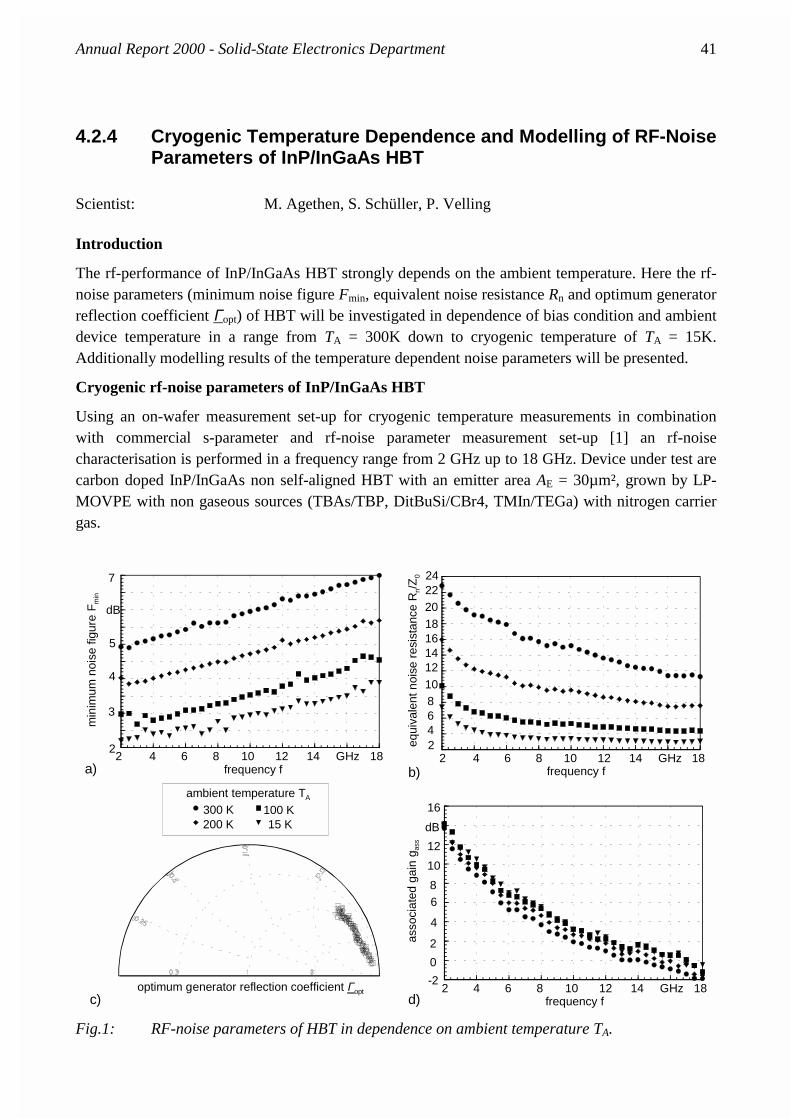
Annual Report 2000 - Solid-State Electronics Department 41
4.2.4 Cryogenic Temperature Dependence and Modelling of RF-Noise Parameters of InP/InGaAs HBT
Scientist: M. Agethen, S. Schüller, P. Velling Introduction
The rf-performance of InP/InGaAs HBT strongly depends on the ambient temperature. Here the rf-noise parameters (minimum noise figure Fmin, equivalent noise resistance Rn and optimum generator reflection coefficient Γopt) of HBT will be investigated in dependence of bias condition and ambient device temperature in a range from TA = 300K down to cryogenic temperature of TA = 15K. Additionally modelling results of the temperature dependent noise parameters will be presented.
Cryogenic rf-noise parameters of InP/InGaAs HBT
Using an on-wafer measurement set-up for cryogenic temperature measurements in combination with commercial s-parameter and rf-noise parameter measurement set-up [1] an rf-noise characterisation is performed in a frequency range from 2 GHz up to 18 GHz. Device under test are carbon doped InP/InGaAs non self-aligned HBT with an emitter area AE = 30µm², grown by LP-MOVPE with non gaseous sources (TBAs/TBP, DitBuSi/CBr4, TMIn/TEGa) with nitrogen carrier gas.
3
dB
7
2 4 6 8 10 12 14 GHz 18frequency f
min
imum
noi
se fi
gure
Fm
in
asso
ciat
ed g
ain
g ass
4
2
5
2 4 6 8 10 12 14 GHz 182
24
frequency f
equi
vale
nt n
oise
res
ista
nce
Rn/
Z0
18
12
64
810
1416
2022
2
dB
16
2 4 6 8 10 12 14 GHz 18frequency f
4
-2
6
0
8
10
12
optimum generator reflection coefficient Γopt
a) b)
d)c)
ambient temperature TA
300 K200 K
100 K15 K
Fig.1: RF-noise parameters of HBT in dependence on ambient temperature TA.

42 Annual Report 2000 - Solid-State Electronics Department
The carbon doped p-(InGa)As:C base (p > 1019cm-3) is compositionally graded to increase current gain (here: B > 400) and transit frequency (here: fT > 65 GHz) and a high temperature in-situ annealing sequence is carried out in TMAs/N2 ambient at T > 600°C to activate the carbon doping in the base [2]. Fig.1 shows the measured rf-noise parameters for four different ambient temperatures (TA = 300K, 200K, 100K, and 15K) but identical collector currents IC as well as collector-emitter voltage VCE. With decreasing temperature the investigated device shows better rf-noise performance. This is demonstrated for the minimum noise figure Fmin (fig. 1a) and equivalent noise resistance Rn (fig. 1b), which both decrease with lower temperature but constant collector current of IC = 10 mA. The optimum generator reflection coefficient Γopt (fig. 1c) as well as the associated gain gass (fig. 1d) show only weak influence on temperature for identical bias condition.
The consistent small-signal and rf-noise model
Fig. 2 shows the “T”-like consistent small-signal and rf-noise model of HBT, based on temperature noise modelling of noisy impedances [3]. Consequently, equivalent noise temperatures are associated to all resistances. Using this model, both, s-parameters as well as noise-parameters can be modelled simultaneously and the different noise phenomena can be correlated directly to specific HBT regions. The noise due to the parasitic resistances is assumed to be thermal noise only, and therefore their equivalent noise temperature is equal to the ambient temperature TA during measurement.
CIO
Cfb
Cjc
Cje
CBP
RBP,TA
LB
CIN
LE
LC
COUT
i
ie
α0iee-jωτ
intrinsic HBT
B
E E
C
RB,TA
Rbb,Tbb
Rjc,TjcRje,
Tje
RE, TA
RC,TA
Rcc,Tcc
Fig.2: The consistent small-signal and rf-noise equivalent circuit of HBT.

Annual Report 2000 - Solid-State Electronics Department 43
Modelling of rf-noise parameters
All model parameters are found using evolutionary optimisation algorithm. A comparison of measured and modelled noise parameters is given in fig.3, showing minimum noise figure Fmin (fig.3a) and equivalent noise resistance Rn (fig.3b) in dependence on ambient measurement temperature TA for constant collector current IC = 20 mA. The excellent agreement between measured and modelled parameters can clearly be seen and demonstrates the capability of the consistent model.
4.5
dB
8.5
2 4 6 8 10 12 14 GHz 18frequency f
min
imum
noi
se fi
gure
Fm
in
5.5
3.5
6.5
2 4 6 8 10 12 14 GHz 180
30
frequency f
equi
vale
nt n
oise
res
ista
nce
Rn/
Z0
5
10
15
20
a) b)
25
ambient temperature TA
300 K200 K
100 K15 K
Fig.3: Measured and modelled rf-parameters of the investigated HBT (symbols: measured data; solid lines: modelled data).
References:
[1] H. Meschede et al. "On-Wafer Microwave Measurement Set-up for Investigation on HEMT’s and High Tc Superconductors at Cryogenic Temperatures Down to 20 K", IEEE Transactions on Microwave Theory and Techniques, Vol. 40, No. 12, 1992
[2] P. Velling, et al. "A comparative study of GaAs- and InP-based HBT growth by means of LP-MOVPE using conventional and non gaseous sources", to be published in “Progress in Crystal Growth and Characterization of Materials”, Dec. 2000.
[3] M. Agethen et al. "Small-Signal and RF-Noise Modelling of InP/InGaAs HBT", Proc. of “EDS HBT-Workshop & 12th III-V Semiconductor Device Simulation Workshop”, Duisburg, Germany, October 2000

44 Annual Report 2000 - Solid-State Electronics Department
4.2.5 Bias Dependent RF-Noise Parameter Modelling of Carbon Doped InP/InGaAs HBT
Scientist: M. Agethen, S. Schüller, P. Velling Introduction
The design of complex high-frequency analogous electronic circuits is very difficult and strongly depends on the models used for the single device. In case of HBT quantitative small-signal modelling has been done, but the modelling of rf-noise parameters (minimum noise figure Fmin, noise equivalent resistance Rn and optimum generator reflection coefficient Γopt) is critical, because e.g. not all noise parameters can be described by established models [1]. The method presented here uses a physically relevant “T”-like small-signal equivalent circuit instead of “p”-like model for small-signal as well as noise modelling, which localises various intrinsic noise sources to specific HBT device regions. A detailed description of this model is presented in this annual report. Here, the bias dependent rf-noise parameter modelling will be presented, including a detailed investigation of the intrinsic noise sources.
Measurement set-up and investigated devices
Using an on-wafer measurement set-up in combination with commercial HP8519C s-parameter and ATN NP5 rf-noise parameter analyser, both s-parameter and rf-noise characterisation is performed in a frequency range from 45 MHz up to 40 GHz and 2 GHz up to 18 GHz, resp. Devices under test are carbon doped InP/InGaAs non self-aligned HBT with an emitter area AE = 30µm², grown by LP-MOVPE with non gaseous.
RF-parameter modelling
As a first result fig.1 shows the excellent capability of the model used to describe s-parameters of HBT in the whole measured frequency range up to 40 GHz. Here, the measured and modelled s-parameters at collector-emitter voltage VCE = 1.2 V in active device region and collector current IC = 2 mA are presented. The symbols represent the measured data, the solid lines the modelled values. Bias dependent measurements are performed and the good agreement between measured and modelled data was achieved.
To prove the consistency with rf-noise parameter modelling, fig.2 to fig.4 show the measured and modelled rf-noise parameters for three different bias conditions at constant collector-emitter voltage VCE = 1.2 V and various collector currents from IC = 2 mA up to IC = 20 mA. The small-signal equivalent elements are extracted by small-signal modelling and kept constant during noise-parameter optimisation. Only the four intrinsic noise equivalent temperatures are optimised.
First of all, the excellent agreement between measured and modelled data can clearly be seen for all three noise parameters. For the minimum noise figure Fmin, a strong increase with rising collector current is obvious (fig.2). The normalized equivalent noise resistance rn = Rn/Z0 (fig.3) shows the same dependence on collector current IC. A minor influence of the collector current is found for the optimum generator reflection coefficient Γopt (fig. 4).

Annual Report 2000 - Solid-State Electronics Department 45
5.0
0.4
1.0
2.0
0.5
-j1.
0
-j2.0
-j0.4
3
dB
8
2 4 6 8 10 12 14 GHz 18frequency f
min
imum
noi
se fi
gure
Fm
in
4
2
1
5
6
collector current IC
2 mA10 mA20 mA
Fig.1: Measured (o) and modelled ( ) Fig.2: Measured (symbols) and modelled
s-parameters in frequency range (lines) minimum noise figure for from 45 MHz up to 40 GHz. constant VCE = 1.2 V.
10
2 4 6 8 10 12 14 GHz 18frequency f
4
2
0
6
8
collector current IC
2 mA10 mA20 mAno
rm. e
quiv
. noi
se r
esis
tanc
e R
n/Z
0
optimum generator reflection coefficient Γopt Fig.3: Measured (symbols) and modelled Fig.4: Measured (symbols) and modelled
(lines) normalized equivalent noise (lines) Γopt for constant VCE = 1.2 V. resistance rn = Rn/Z0 (VCE = 1.2 V).
Investigation of intrinsic noise sources
As a result of the above mentioned small-signal and rf-noise parameter model a localization of various noise sources in the specific device regions is possible. With the optimisation results, the spectral densities of the four intrinsic noise current sources can be calculated and investigated in dependence of bias condition. The following formula is used for calculation of the intrinsic noise currents due to optimised model parameter values, here resistance Rx and equivalent noise temperature Tx (with index “x” for all various intrinsic noise sources):
x
xn,x R
Ti k4= . (1)
These calculated values are now plotted in dependence on bias condition, here we calculate the base iB,S and collector iC,S shot noise currents due to dc values with:
BS,B eIi 2= , (2)
CS,C eIi 2= . (3)
Fig.5 shows the intrinsic base noise current ibb,n in dependence on base shot noise current iB,S. The intrinsic base noise current shows a linear dependence on extrinsic dc base current. But a very high

46 Annual Report 2000 - Solid-State Electronics Department
offset is obvious, which is correlated to the intrinsic base noise source and has to be investigated in more detail.
0 1 2 3 4
8
10
14
6Hz/pA
intr
insi
c ba
se n
oise
cur
rent
i bb,
n
base current shot noise iB,S
Hz
pA
0 15 30 45 60
0
20
120
90Hz/pA
intr
insi
c ba
se-e
mitt
erno
ise
curr
ent i
je,n
collector current shot noise iC,S
Hz
40
60
80
pA
Fig.5: Extracted (• ) intrinsic base noise Fig.6: Extracted (• ) intrinsic base-emitter
currents in dependence on base junction noise currents in dep. on current shot noise (VCE = 1.2 V). collector current shot noise.
0 1 2 3 40
2
6
6Hz/pA
intr
insi
c ba
se-c
olle
ctor
nois
e cu
rren
t ijc
,n
base current shot noise iB,S
Hz
pA
1
3
Fig.7: Extracted (• ) intrinsic base-
collector junction noise currents in dependence on base current shot noise for constant VCE = 1.2 V. Solid line represents linear fit.
Fig.6 now shows the intrinsic base-emitter junction noise current ije,n in dependence on collector shot noise iS,C. This intrinsic noise source depends linearly on collector current IC. The gradient is nearly equal to but slightly higher to one.
The two last intrinsic noise current sources show only minor influence and bias dependence. The values of intrinsic collector noise current icc,n are very low ( )HzpAi n,cc 2< and independent on extrinsic currents. The intrinsic base-collector noise current ijc,n is equal to the shot noise current of the dc base current (fig.7).
Conclusion
A bias dependent investigation of small-signal and rf-noise parameters of InP/InGaAs HBT is presented. The excellent agreement between measured and modelled data is clearly demonstrated and a localization of intrinsic noise sources to specific device regions is made. This localization allows a detailed investigation of the physical noise phenomena in the device.
References: [1] A. Huber et al.
"RF Noise Characterization of a high performance InP/InGaAs HBT", Conf. Proc. of the 20th Workshop Compd. Semicond. Device Integr. Circuits, 1996, Lithuania, pp. 83-84

Annual Report 2000 - Solid-State Electronics Department 47
4.2.6 A New Consistent and Scalable PSPICE Model for Enhance-ment- and Depletion-Type HFET
Student: S. Schüller Scientist: R.M. Bertenburg, M. Agethen, A. Brennemann Introduction
For simulation of digital circuits realized in Direct Coupled FET Logic (DCFL) using depletion-
type as well as enhancement-type Heterostructure-Field Effect Transistors (HFET) a consistent
model is necessary that is able to describe both types of transistors. We developed a new analytical
large-signal model for enhancement- and depletion-type HFET. Based on Analog Behavioral
Modeling modul (ABM) for the voltage-controlled current source and capacitance models this
model takes into account all relevant intrinsic and parasitic effects and considers the frequency
behaviour of the investigated devices as well. The scaling capability of this model with respect to
the gate length and the gate width is also possible.
The new consistent and scalable model
The new consistent HFET model is an electrical large-signal equivalent circuit, that was implemented in the simulation software PSPICE in form of sub circuit description. The diode characteristic of the Schottky contact at the gate is realized by two diodes, the gate-drain and the gate-source diode. For both diodes the model parameters of the diode model implemented in PSPICE are fitted to real measured data. Fig.1 shows the electrical large-signal equivalent circuit. The most important module is the mathematical description of the voltage-controlled output current source, which is based on an Analog Behavioral Modeling modul (ABM).
RS
RG
RD
gate-source diode
Drain
Source
drain-source capacitance CDS = f(VDS')
gate-drain diode
RGK
gate-drain capacitanceCGD = f(VGD')
gate-source capacitance CGS = f(VGS')
I D
Gate
G'
D'
S'
ABM: Analog Behavioral ModelingPSPICE: PSPICE Model
PSPICE
PSPICE
ABM
ABMABM
ABM
Fig.1: Electrical large-signal equivalent circuit The complete analytical description of this current source takes into account all intrinsic and parasitic effects, as gate-leakage current, current limiting and current compression as well as kink effect due to impact ionisation:

48 Annual Report 2000 - Solid-State Electronics Department
)))(tanh(1(21
TGSGSD VVaVI −⋅+⋅⋅= switch: on/off state
))||)(tanh((( 0
0DSGSGS
b
g
g VVVsigndcLL
W
W⋅⋅⋅−⋅⋅
⋅⋅ β output branch
))((tanh( minVVVe TGS −−⋅⋅ current compression )))(tanh( maxVVVg TGS −−⋅− current limiting
DSVmDSTGS
g eVVVlW
Wk ⋅⋅⋅−⋅⋅
⋅+ ))(tanh(
2
0 impact ionization
)))tanh(1(
)))(tanh(1(
2
10
2
GSkDS
GSKGSg
VpVVn
VVVaW
W
⋅−−⋅+⋅
⋅−⋅+⋅⋅+ β kink effect
(1)
Comparison of measured and simulated data
The model parameters used can be extracted from real measured transistor data using a simple procedure. First the well known parameters like VT, Wg=W0 and Lg=L0 have to be set. The next step is to find the right transconductance β at VGS = 0, the parameters c and d from transition between ohmic and saturation regime, e and Vmin from current compression, analogous g and Vmax from current limiting. The linear current increase has to be fitted by setting the parameter k, analogous the parameter m for the exponential current increase due impact ionisation in saturation regime. In case of kink effect the next parameters have to be set in the following order: transconductance β2, Vk1 and Vk2 are the turn on kink voltages and at the end the parameters n and p. The output characteristic of a typical depletion-type HFET is shown in fig. 2, the excellent agreement between measured and simulated data can clearly be seen.
0 0.5 1 1.5 V 2.5
-5
0
5
10
15
mA
25
V'DS
ID
Fig.2: Output characteristic of a DHFET with Wg = 80µm and Lg = 0.7µm measured ( ) and simulated (-) data The scaling capability with respect to the gate width Wg and the gate length Lg of the complete HFET model is given in fig. 3 a) and b), resp. Here, as an example, the output characteristics of the E-HFET are given. The model parameters have been extracted for an E-HFET with a gate width of W0 = 80µm and a gate length of L0 = 0.7µm.
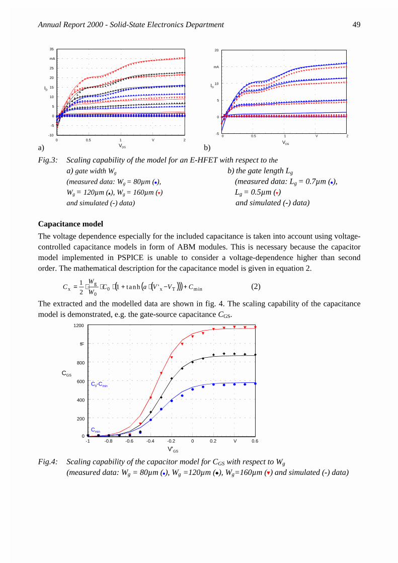
Annual Report 2000 - Solid-State Electronics Department 49
a)0 0.5 1 V 2
-10
-5
0
5
10
15
20
25
mA
35
VDS
ID
b)
0 0.5 1 V 2
VDS
ID
-5
0
5
10
mA
20
Fig.3: Scaling capability of the model for an E-HFET with respect to the
a) gate width Wg b) the gate length Lg
(measured data: Wg = 80µm ( ), (measured data: Lg = 0.7µm ( ), Wg = 120µm ( ), Wg = 160µm ( ) Lg = 0.5µm ( )
and simulated (-) data) and simulated (-) data)
Capacitance model
The voltage dependence especially for the included capacitance is taken into account using voltage-controlled capacitance models in form of ABM modules. This is necessary because the capacitor model implemented in PSPICE is unable to consider a voltage-dependence higher than second order. The mathematical description for the capacitance model is given in equation 2.
( )( )( ) minTx00
gx 'tanh1
21
CVVaCW
WC +−⋅+⋅⋅⋅= (2)
The extracted and the modelled data are shown in fig. 4. The scaling capability of the capacitance model is demonstrated, e.g. the gate-source capacitance CGS.
-1 -0.8 -0.6 -0.4 -0.2 0 0.2 V 0.60
200
400
600
800
fF
1200
V'GS
CGS
C0-Cmin
Cmin
Fig.4: Scaling capability of the capacitor model for CGS with respect to Wg (measured data: Wg = 80µm ( ), Wg =120µm ( ), Wg=160µm ( ) and simulated (-) data)
50 Annual Report 2000 - Solid-State Electronics Department
4.2.7 Magneto Transcondcutance Mobiliy Profiling carried-out using the HP 4145 Parameter Analyser
Scientist: W. Prost Technical Assistance U. Doerk Introduction
Magneto transconductance mobility profiling is a powerful tool in order to analyse the mobility in FET channels as a function of the applied bias [1]. The principal advantage of this method is the applicability to structures where HALL measurements can not be used for transport characterisation:
(1) FET devices with highly doped cap layers [2],
(2) FET channel which need applied bias in order to open the channel (enhancement type FETs).
In this contribution it will be shown, that the HP 4145 Parameter Analyser in the long integration time mode is sufficient for the analysis and can replace the formerly used Lock-In Amplifier. This way, the magneto transconductance mobility profiling is directly available during the DC test of the devices. The new approach is adopted in order to determine the channel mobility of a pseudomorphic InGaAs channel heterostructure field effect transistor on GaAs substrate.
Mobility Profiling Measurement Technique
Applying a magnetic field B to the channel of a FET, the geometric magneto-resistance effect reduces the conductivity of the channel. The transconductance can be measured in order to get this information with a kind a depth resolution defined by the applied gate bias [1]. The drain bias has to be low in order to assure a low-field ohmic transport. Under these conditions the mobility can be deduced from the transconductance dependence on the magnetic field:
(1) ( )
( )µ = −=1
10
1 1B
g B
g Bm
m
.
The deduced mobility (eq. 1) can be evaluated in dependence of the applied gate-source voltage. In 2DEG samples the mobility is affected by the shielding effect of accumulated carriers against the ionised donors in the donor layer. Hence, especially at low temperatures a depleted channel exhibits a much lower mobility than an open channel. At room temperature the polar-optical phonon scattering limits the mobility and the gate bias dependence is reduced.
The gate-modulated sheet carrier concentration can be calculated at each bias point using the corresponding mobility and transconductance data:
(2) ( ) ( )( )dn V
g V
V
L
W VdVS GS
m GS
GS DSGS= ⋅ ⋅ ⋅
µ1
.
Using a multiple channel model and the Hall-equivalent mobility µH can be deduced from eq. 1, 2 [3] while taking care of the Hall factor because the magneto-transconductance method delivers the

Annual Report 2000 - Solid-State Electronics Department 51
drift mobility. By summing up the gate-modulated sheet carrier concentration from pinch-off to build-in voltage the whole sheet carrier concentration of the channel can be calculated:
(3) ( )n dn Vs
V
V
S GS
T
P
= ∫ , and transferred to a summation ( )nV
dn VsGS ii
k
S i GS i= ⋅=∑ 1
1 ∆ ,, , .
Pseudomorphic InGaAs/AlGaAs/GaAs HFET
The sample was provided by the company United Monolithic Semiconductors (UMS, Dr. M. Camiade). The gate length is 0.25 µm. A device with T-shaped geometry and a gate width of 2 x 20 µm was selected. The pinch-off value is about VGS = -0.4 V. All I-V measurements are made with a semiconductor parameter analyser in the long integration time mode. The transfer characteristic is measured using different drain bias conditions ranging from 0.05 V to 0.1 V and with two magnetic fields of 0.5 T and 1 T. These measurements are the basis for all calculated transconductance, mobility and carrier density results. The transconductance is calculated using five different gate bias steps according to 100 mV bias swing. The maximum transconductance is obtained at -0,25 V gate bias and the value of 10 mS corresponds to 250 mS/mm at VDS = 0.1 V. According to Eq. 1 the mobility has been calculated at each gate-bias point from the transconductance reduction in the presence of a magnetic field. Within the investigated drain bias no substantial modification has been obtained such that it can be concluded that all measurements represent the ohmic regime.
Fig. 1: Mobility Profile deduced from I-V data taken at zero and 1 Tesla magnetic field According to eq. 2 [2] the gate modulated carrier concentration can be evaluated (cf. Fig. 2). By summing up the differential concentration (eq. 3) the total Hall equivalent concentration is calculated to 4.3.1011 cm-2. The intrinsic transconductance is calculated with the assumption that the "intrinsic" output conductance can be calculated from the measured I-V data:
(4) gg
R R R gm intm ext
s D M d,
,
( )=
− + + ⋅1.
0,00
0,10
0,20
0,30
0,40
0,50
0,60
-0,40 -0,20 0,00 0,20 0,40
gate-source voltage Vgs / V
mo
bili
ty µ
/m²/
Vs
VDS = 0,05 V
VDS = 0,075 V
VDS = 0,1 V

52 Annual Report 2000 - Solid-State Electronics Department
The parasitic resistance are the lead resistance between source and gate RS and gate and drain RD and the resistance of the measurement set-up RM. Assuming the total parasitic resistance to: RS + RD + RM =12 Ω, we can calculate the "intrinsic" gate modulated carrier density dns,int which is also plotted in Fig. 2. Accordingly, a Hall equivalent channel concentration of ns = 5.7.1011 cm-2 has been calculated.
Fig. 2: Calculated profile of gate modulated carrier concentration at VDS = 50 mV. The intrinsic concentration has been calculated for a parasitic resistance of 12 Ohm.
The computation of the whole channel concentration is affected by the high output conductance in the ohmic regime. That means that there is a very conductive path parallel to the current source in the small-signal equivalent circuit of the FET [3 ]. Due to the high output conductance the measured extrinsic transconductance exhibits a high error rate. Hence, the given data are assumed to be too low. A larger gate length may simplify the concentration analysis.
Summary
A full set of transport data from a pseudomorphic InGaAs/AlGaAs/GaAs HFET is provided by bias dependent magneto transconductance measurements. The channel mobility of the device in the presence of highly conductive cap layers is correctly evaluated. The HALL-equivalent evaluation of the channel concentration is assumed to result in a reduced channel concentration due to a highly conductive output resistance in the ohmic regime.
References:
[1] P.R. Jay, R.H. Wallis, "Magneto transconductance mobility measurements of GaAs MESFETs", IEEE Electron Dev. Lett., vol. 8, no. 10, 1981.
[2] W.Prost, W.Brockerhoff, K.Heime, K.Ploog, W.Schlapp, G.Weimann, H.Morkoc; "Gate-Voltage Dependent Transport Measurements on Heterostructure Field-Effect Transistors", IEEE Trans. Electron Devices, vol. ED-33, pp.646-650, 1986.
[3] W.Prost, W.Bettermann, K.Heime, I.Gyuro, H.Dämbkes, M.Heuken, G.Weimann, W.Schlapp; "HALL-equivalent determination of carrier mobility and concentration in SQW-, MQW- and HIG-FET channels", Inst. Phys. Conf. Ser. No. 106, pp.501-506, 1989.
0
1E+14
2E+14
3E+14
4E+14
5E+14
6E+14
7E+14
8E+14
9E+14
-0,40 -0,30 -0,20 -0,10 0,00 0,10 0,20 0,30 0,40
Gate-source voltage VGS / V
mo
du
late
d s
hee
t co
nce
ntr
atio
n d
ns
/ m-2
dns
dns,int

Annual Report 2000 - Solid-State Electronics Department 53
4.2.8 High Frequency Measurement Set-Up for Analog and Digital Circuits in Time Domain
Scientists: H. van Husen, A. Brennemann 1. Introduction
So far at HLT high frequency measurements are focused on single devices like heterosturcture field-effect transistors (FET), heterojunction bipolar transistors (HBT) and resonant tunneling diodes (RTD). To expand our facilities for high frequency measurements in time and frequency domain, we additionally built up a measurement setup to characterize digital circuits. This will lead to design circuits of higher complexity with a larger number of electronic devices and modules.
2. Experimental-set-up
The measurement-setup consists of a pulse generator HP8133A, a digital oscilloscope HP54750A, two DC power supply HP E3631A and the measuring station Cascade Microtek Summit 9000 (fig. 1). The pulse generator provides frequencies up to 3.5 GHz. The Digital Oscilloscope acts as a mainframe and its two slots are equiped with HP 54752A 2-channel plug-in modules. Each module has two input channels with 50 GHz selectable channel bandwidth, 1 – 100 mV/div sensitivity and 50 input impedance. The external trigger bandwidth of these modules is limited to a maximum frequency of 2.5 GHz. For power supply a maximum of five different voltages is available. Four positioners ensure, that the circuits can be contacted in a very flexible way. All tips are specified up to 40 GHz, cables up to 7 GHz. The devices are controlled by several computer programs, which are developed with the visual engineering environment HP VEE. A block diagram of the set-up is shown in fig. 2.
Fig.1: measurement-set-up

54 Annual Report 2000 - Solid-State Electronics Department
Fig. 2: block-diagram of the measurement set-up
3. Measurements
Various digital circuits like inverters, frequency dividers, ring oscillators and a 1-bit full-adder were investigated with above measurement-set-up. Here we will present the results of a frequency divider: one was conventionally designed and the other was designed in cooperation with Dr. E. Bushehri from the Middlesex University, London (fig. 3), using non-linear negative feedback (NNFB) to avoid a static current flow into the following gates.
Fig.2: circuit-layout and SEM of a frequency divider in conventional (left) and "Bushehri design" (right)
Sp annung s-que llen
Sp annung s-que llen
Dig ita l-O szilloskop
Signa l-G enerator
D ig ita lm essp latz
HP-Inter face Bus
Sig na l-le itungen
Steuerung se be neG erä teebeneM e ssebe ne

Annual Report 2000 - Solid-State Electronics Department 55
At the left handside the circuit-layout in conventional design with the corresponding SEM picture is shown, at the right handside a frequency divider in the Busheri layout. In conventional design nine logic gates are necessary, whereas in the other layout the number of gates can be reduced to six. On each SEM picture (upper right corner) an output-buffer is seen. This output-buffer is added to the design to enable the measurement of the output signal at a measurement-
input impedance.
Fig. 4 and Fig. 5 show the input- and ouput-signal of each design at a distinct frequency. The normal line represents the input-signal with frequency f and amplitude AV . The bold line is the measured output-signal with a decreased amplitude mainly caused by a 10dB-attenuator before the input channel to protect the digital oscilloscope. 21 , DDDD VV and SSV are supply voltages. Additional measurements show, that 80% of all frequency dividers with conventional design works very well over the frequency range from 50 MHz to 3.4 GHz, even if the amplitude AV decreases to a minimum of 0.3 V. Fig. 5 shows the results for a divider in Bushehri design.
Fig. 4: frequency divider − conventional design Fig. 5: frequency divider − Bushehri design
4. Outlook
In future we want to combine serveral dividers to reduce frequency by a factor 4 or 8. Another idea is to add the frequency divider to our ring oscillator design. In this case the circuit provides by itself a trigger frequency, that matches the input bandwidth of the oscilloscopes external trigger input. Then it would be possible to measure the ring oscillator in time domain above the frequency of 2.5 GHz, which is now restricted by the external trigger input bandwidth of the oscilloscope.
0,0 0,5 1,0 1,5 2,0
-0,6
-0,4
-0,2
0,0
0,2
0,4
0,6
0,8
1,0
1,2
f = 3.4 G Hz, V A=1.0 V
VD D 1 = VD D 2 = 2.0 V, V SS = -2.2 V
ID D 1 = 37 m A, ID D 2 = 25 m A, ISS = 34 m A
input
output
am
plit
ud
e V
A [
V]
time [ns]
0,0 0,5 1,0 1,5 2,0-0,1
0,0
0,1
0,2
0,3
f = 3.0 G Hz, V A=0.8 V
VDD 1 = V DD 2 = 2.0 V, VSS = -2.0 V
input
output
am
plit
ud
e V
A [
V]
time [ns]

56 Annual Report 2000 - Solid-State Electronics Department
4.2.9 Optical Characterization of Channel Waveguides and Devices
Student: Murat Ylmaz Supervisors: Marcin Swillo and Lech Wosinski (Royal Institute of Technology,
Stockholm Sweden) W. Brockerhoff
Introduction
This report is the result of a research project of an ERASMUS student exchange project, carried out at the Royal Institute of Technology, Stockholm, Sweden.
The aim of this project was to develop a method for optimising the coupling efficiency between a single mode fiber and a silica-based channel waveguide. For the calculation of the coupling efficiency, a set-up for mode profile characterization had to be build up and programs for the evaluation of the measured modal intensity distribution had to be written. Within the scope of the work, in addition, a simulation program has been written for the calculation of the modal fields of differently shaped waveguides to optimise the waveguide and the refractive index profile in such a way as to increase the coupling efficiency.
Experimental set-up
The set-up for measuring the mode profile of the waveguides and fibers is sketched in figure1. The light source was provided by a 1.55 µm InGaAsP/InP distributed feedback (DFB) laser diode. The laser diode was controlled by the LDC-3744 laser controller from Hewlett Packard. The laser beam has been launched into a single mode fiber and was guided to the front of the waveguide. By means of a micro positioner stage, the light beam was coupled into the waveguide. Since the dimensions of the waveguide are in the micrometer range, the image of the surface of the waveguide had to be magnified. For this purpose a 63x objective from Melles Griot with a numerical aperture of 0.85 and an additional telescope have been used. Thus, a magnification of 240 times has been achieved. The image was focused onto the infrared camera MicronViewer 7290A from Electrophysics. And finally, the image was converted to digital data by means of the frame grabber PX 610 from imagination for further data analysis.

Annual Report 2000 - Solid-State Electronics Department 57
Fig.1 Experimental set-up for mode profile characterization
Results
The finite difference method as described in [2] has been used to calculate the field patterns of differently shaped waveguides. Fig.2 shows a quadratic waveguide with a dimension of 5.8 µm. The coupling efficiency between the fiber and the quadratic waveguide has been calculated as 93 %.
Fig.2 Calculated field profile of a quadratic waveguide
The next figure shows the calculated field pattern of the fabricated waveguide, which has a trapezoidal shape due to the fabrication process. The coupling efficiency has been determined as 86 %.
1.0 0 2.0 0 3.0 0 4.0 0 5.0 0 6.0 0 7.0 0 8.0 0 9.0 0 10.00 11.00
1.0 0
2.0 0
3.0 0
4.0 0
5.0 0
6.0 0
7.0 0
8.0 0
9.0 0
10.00
11.00
1.0 0 2.0 0 3 .00 4.0 0 5.0 0 6.0 0 7 .00 8.0 0 9.0 0 10 .0 0 11.00
1.0 0
2.0 0
3.0 0
4.0 0
5.0 0
6.0 0
7.0 0
8.0 0
9.0 0
10.0 0
11.0 0

58 Annual Report 2000 - Solid-State Electronics Department
Fig.3 Calculated field profile of trapezoidal waveguide
The effective numerical aperture of the simulated waveguides was about 0.16.
Fig.4 shows the field intensity distribution of the single mode fiber SMF-28-J9 from Corning Inc. as it is been measured with the mode profile characterization set-up. The accuracy of the system has been estimated by comparing the spot size, extracted from this picture, with the spot size given by the manufacturer. Thus, the accuracy of the system has been determined as less than 16 %, which is close to the accuracies of similar systems, which were about 10 % [2].
Fig.4 Field intensity distribution of the SMF-28-J9
The next figure shows the intensity distribution of a trapezoidal waveguide. The coupling efficiency between the single mode fiber and the fabricated waveguide has been determined as 95 % ± 3 %, which is quite good compared to other results (80-96 %) in the literature [2].
2 .00 4.0 0 6.00 8 .00 10 .00 12.0 0
2.00
4.00
6.00
8.00
10.00
12.00
2.00 4.00 6.00 8.00 10.0 0 12.0 0
2.00
4.00
6.00
8.00
10.0 0
12.0 0
2 .00 4 .00 6 .00 8 .00 1 0.0 0 1 2.0 0 1 4.0 0 1 6 .00
2 .00
4 .00
6 .00
8 .00
1 0.0 0
1 2.0 0
1 4.0 0
1 6.0 0
2 .00 4 .00 6 .00 8 .00 1 0.0 0 1 2.0 0 1 4.0 0 1 6 .00
2 .00
4 .00
6 .00
8 .00
1 0.0 0
1 2.0 0
1 4.0 0
1 6.0 0

Annual Report 2000 - Solid-State Electronics Department 59
Fig.5 Intensity distribution and contour of the silica-based channel waveguide
Conclusion
The simulation of the waveguides revealed that the coupling efficiency can be increased up to 93 % for squared waveguides. The program can be used to optimise the waveguide and the refractive index profile for the optimum coupling efficiency. The performed investigation proved the feasibility of the developed system for determining the coupling efficiency between fibers and designed waveguides.
Acknowledgement
I would like to thank my supervisors in both countries for their support. Many thanks to Jayanta K. Sahu, H. Fernando and M. Dainese for providing me with the waveguides and special thanks to A. Kévorkian for private communications regarding the simulation program.
References
[1] D.R. Heatley, G. Vitrant and A. Kévorkian
"Simple finite-difference algorithm for calculating waveguide modes"
Optical and Quantum Electronics, 26, pp. 151-163, 1994
[2] Alexandre de A.P. Pohl
"Feldangepaßte Eingangswellenleiter für verlustarme Faser-Chip-Verbindungen im InGaAsP/InP-Materialsystem", VDI-Verlag GmbH, 1994
2.00 4.00 6 .0 0 8.00 10 .0 0 12 .00 14 .00 1 6.00
2.00
4.00
6.00
8.00
10 .00
12 .00
14 .00
16 .00
2.00 4.0 0 6.00 8.0 0 10 .00 12 .00 14 .00 16 .00
2.00
4.00
6.00
8.00
10 .00
12 .00
14 .00
16 .00

60 Annual Report 2000 - Solid-State Electronics Department
4.2.10 Development and Implementing of a Test System to Control a Fractional-N-PLL for a Closed Loop Modulation
Student Th. Kühn Supervisor: R.M. Bertenburg
The work was carried out in cooperation with Infineon Technologies, Angermund, Germany.
Nowadays, the demand on mobile and cordless communications rises quickly. The competition between the developers results in products with increasingly performance and decreasingly power consumption and costs.
Therefore, a new frequency synthesizer concept for a closed loop modulation is analysed. This modulation concept improves the noise immunity and it reduces a possible drift of the transmit frequency compared to a conventional used open loop modulation concept. The components of this new frequency synthesizer concept are shown in fig.1.
P F D LF V C O
divider:N
fref
fdiv
C P
X-data
ndiv
f rac t ional -N-PLL
fout
Gaussfilter
compensat ion f i l terorL P
Σ∆-modula tor
digi tal adaptat ion unit
Cw
Fig.1: Frequency synthesizer concept for a closed loop modulation
The frequency synthesizer is divided into two parts. The first part is the fractional-N phase locked loop (PLL). It contains the five components phase frequency detector (PFD), charge pump (CP), loop filter (LF), voltage controlled oscillator (VCO) and a divider (divider :N).

Annual Report 2000 - Solid-State Electronics Department 61
The second part of the synthesizer is the digital adaptation unit. It contains a Gauss filter, a compensation filter or a low pass filter (LP) and a Σ∆-modulator. The adaptation unit processes the transmit data (TX-data) and creates the input signal ndiv for the closed PLL. The fractional-N-PLL uses the reference frequency fref and the signal ndiv to generate the output frequency fout of the synthesizer. The transmit channel frequency is chosen by the binary coded channel word (Cw).
The target of this project is the development of the digital adaptation unit and the realization on a test board with a FPGA (field programmable gate array). The FPGA test board is used for test purposes of the whole frequency synthesizer concept.
Two different versions of the adaptation unit are developed. The fig.2 shows the first realization for low data rate.
TX-data ndiv Gaussfilter
Σ∆-modula torL P
w
Fig. 2: Digital adaptation unit for low data rate
The components Gauss filter and low pass filter (LP) reduces the bandwidth of the signal TX-data. The Σ∆-modulator carries out noise shaping of the transmit signal and creates the divider input signal ndiv of the PLL. The noise shaping is done by moving the quantization noise to frequency bands which are not of interest and then removing the high frequency component by the low pass filter characteristic of the PLL.
The second version of the adaptation unit is shown in fig.3. This concept can be used for high data rates.
TX-data ndiv Gaussfilter
Σ∆-modula torcompensat ion f i l ter
w
Fig.3: Digital adaptation unit for high data rate
The signal processing of the Gauss filter and the Σ∆-modulator is the same as in fig.2. The main task of the compensation filter is to compensate the small pass band of the closed fractional-N-PLL. This compensation make possible a high data rate.
The Σ∆-modulator is realized as a 1-1-1- MASH (multi stage noise shaping) structure in both versions of the adaptation unit.

62 Annual Report 2000 - Solid-State Electronics Department
Several steps are necessary to realize the digital adaptation unit on the FPGA test board. A first helpful step is to create a model of each component and test it on his specifications. In this case the programming language C was used to create and test the models. The models consider parameters like the number of used bits of each signal to simplify the implementation in a hardware description language.
After verification of the C-model behaviour follows the implementation of the digital adaptation unit in the hardware description language VHDL (very high speed integrated circuits hardware description language). The VHDL implementation is proved with the leapfrogTM VHDL simulator.
The correctly working VHDL code is used for synthesis by the synthesis tool “fpga-analyzer” from Synopsys. The synthesis transfers the VHDL code into a netlist of logical gates. The synthesis tool is specific configured to implement the synthesis result on the FPGA test board. The FPGA is programmed with the synthesis result and realizes the adaptation unit on the test board. The behaviour of the programmed FPGA is measured with a logic analyser. The comparison of the measure results with the simulation (C-model and VHDL simulation) proves the behaviour of the adaptation unit.
The measurement shows that both implementations of the adaptation unit (fig.2 and fig.3) work correctly.
The result of this work is the realization of two versions of a adaptation unit on a FPGA test board. Furthermore the Test board can be used to generate the divider input signal ndiv for the fractional-N-PLL. Together with a fractional-N-PLL as specified in fig.1, it is possible to test the frequency synthesizer concept for a closed loop modulation.
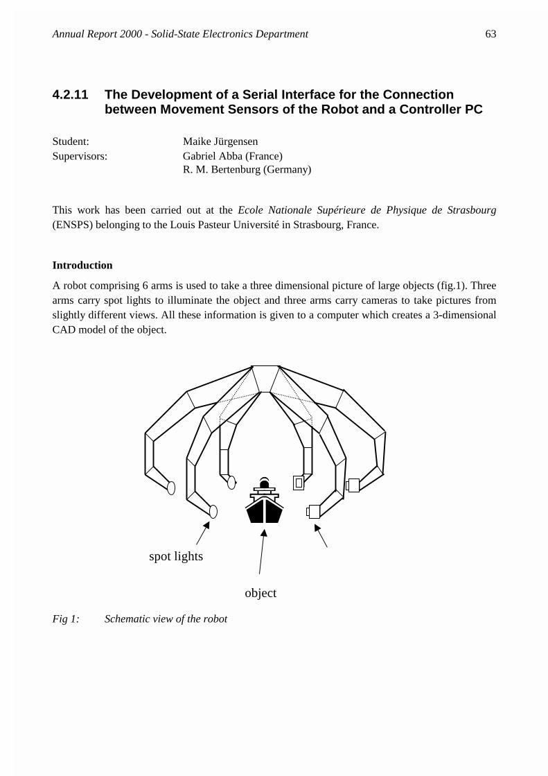
Annual Report 2000 - Solid-State Electronics Department 63
4.2.11 The Development of a Serial Interface for the Connection between Movement Sensors of the Robot and a Controller PC
Student: Maike Jürgensen Supervisors: Gabriel Abba (France) R. M. Bertenburg (Germany)
This work has been carried out at the Ecole Nationale Supérieure de Physique de Strasbourg (ENSPS) belonging to the Louis Pasteur Université in Strasbourg, France.
Introduction
A robot comprising 6 arms is used to take a three dimensional picture of large objects (fig.1). Three arms carry spot lights to illuminate the object and three arms carry cameras to take pictures from slightly different views. All these information is given to a computer which creates a 3-dimensional CAD model of the object.
Fig 1: Schematic view of the robot
spot lights
object

64 Annual Report 2000 - Solid-State Electronics Department
Electrical and mechanical demands
The positioning information of the robot arms have to be transferred to the computer. Every arm consists of 4 axes, each one carrying an angle encoder which delivers three sensor signals. As there are 6 arms we have in total 6 arms * 4 axes * 3 sensors = 72 signals to transfer. Since the robot arms need to be light and flexible the amount of necessary wiring should be as small as possible. Therefore, a two wire serial BUS concept was used. By this means, 72 parallel signals have to be converted into a serial form. Additionally, the interface hardware must be capable to be connected via a BUS interconnection topology. The RS 485 interface fulfills all these necessities.
Due to the BUS structure, the interface between the sensor hardware and the PC must be quite 'intelligent'. It has to detect its individual address and react by transferring the actual angle values to determine the position of the robot arms. A Master-Slave concept is used here to enable stand-alone transfer protocolling and error detection. The Master part is connected to the PC. It sends out the Slave addresses via the serial BUS. The Slave has to detect its address and sends back its address followed by a 19 bit number representing the actual angle value.
Tab 1: Received and transmitted data (bit scheme) by the Slave
Start A4 A3 A2 A1 A0 Reset Parity Stop
1 2 3 4 5 6 7 8 9
start A4 A3 A2 A1 A0 Ref Q9 Q8 Q7 Q6 Q5 Q4 Q3 Q2 Q1 Q0 P stop
1 2 3 4 5 6 7 8 9 10 11 12 13 14 15 16 17 18 19
After that the Slave resets the angle counter and monitors any changes of the angle encoder, again. By this means, only the changes in angle value are transmitted rather than absolute values. Thus, the necessary number range is reduced drastically and accuracy is increased. Tab 1 shows the received and sent data by the Slave.
Realization of the Slave hardware
The complete hardware including all necessary functions is realized by a single Computer Programmable Logic Device (CPLD) by XILINX. This work is mainly focused on hardware-programming using a specialized software development and emulation tool by XILINX. It allows to program the necessary logical functions and to emulate the device behavior after it has been programmed. To give an example fig. 2 and 3 depict two flow diagrams which have been developed. The development tool by XILINX optimises the logic structure internally, so that it fits into the hardware integrated in the CPLD chip. The chip that has been used in this work is a XC9500plcc144 which consists of 144 identical macro cells. The user is able to program the interconnecting switching matrix, and furthermore the function of the macro cells itself. By this means, even highly functional logic blocks can be realized.

Annual Report 2000 - Solid-State Electronics Department 65
This work ended up with a successful simulation of all necessary functions for the above described Master-Slave interface and is now ready for implementation.
Fig 2: The Top Schematic Level

66 Annual Report 2000 - Solid-State Electronics Department
Fig 5: An Example of the Basic Schematic Level

Annual Report 2000 - Solid-State Electronics Department 67
4.3 Device and Circuit Processing and
Characterization

68 Annual Report 2000 - Solid-State Electronics Department
4.3.1 Fabrication of Mushroom Gates in a 2 - Layer Resist System using Electron Beam Lithography
Scientist: Jan Degenhardt
Introduction:
For modern telecommunication application using high electron mobility transistors (HEMTs) it is vital to merge the restrictions of small gate length and small resistivity of the gate to reach highest cut off frequency and best maximum frequency of oscillation. One of the most common designs is the so-called mushroom or T-Gate design, joining together a small footprint and a large, i.e. low resistive head. To achieve such kind of three-dimensional structure different technologies were established years ago. One of these technologies, which based on 3 resist layers, was recently used in our group. To allow more flexible gate layouts and by simplifying the process technology a 2 layers resist process for electron beam lithography was introduced.
Resist Layer Stack
E-Beam lithography especially in the mid-energy regime and above don't allow any separate exposure of upper and lower resist areas during the lithography process which would cast out a three dimensional profile. Electrons with energy more than a few kV always penetrate the entire cross section of the resist and don't leave any control in the vertical direction. Using resist layers with two different sensitivities instead of one uniform layer gives the opportunity to handle the bottom layer selective from the upper layer just by choosing the dose of the electrons in the right interval. On the other hand the dose for the head exposure (upper layer) must be high enough to get a sufficient under-cut to the upper layer going along with clear metal cut off during the gate metal lift-off process. This additional restriction allows skipping the third layer, which one is commonly used to get hold on the lift off process.
Gate Width Determination:
Part of this work was it to get a detailed knowledge of the dose window limited by the restriction of clearing dose and profile under cut. With a new developed programme that could use the mark alignment scan of a JEOL-RAITH Lithography system to gather information of the gate profile it was possible to inspect the profile of many gates automatically. Process control and also mass screening for dose variation test can be easily performed and allow exact knowledge of the dose window for a two layer resist system as it will be used for our T-Gates. In an experiment to evaluate the changes in the gate foot print and head size a variation of 120 gates was exposed in an array. After development, line scans orthogonal to the gates was used to display the micrograph brightness profile of any gate. Using the micrograph profiles the software works out the foot width of any individual T-Gate which is depicted in fig.1.

Annual Report 2000 - Solid-State Electronics Department 69
Fig1: This plot shows a variation of head and foot dose of T-Gates indicating different gate lengths. The gate layout was designed with a 150nm foot print using a resist system consisting of PMMA 950k04 (240nm) as bottom layer and MMA 6% (450nm) for the top layer.
As can been seen in fig.1 the three dimensional plot consists of an intersection of two dose planes. One of them with a small slope and one with higher slope. The intersections of both determine the limitations of smallest gates that could be exposed with the current design of 150nm wide foot prints. Doses less than these for the foot or the head will cause a not cleared foot print where only a bottom closed trench in the resist remains without any usage for gate recess and metalisation. The borderline of gate width is mainly related to the geometrical design in conjunction with the forward scattering of electron on the path through the resist. Less exposure dose will turn out a shallower trench but keeping nearly the width. The other plane with higher slope shows the variation of gate length with head and foot dose in a regime where the gate is usable. The widening of the gate foot is chiefly determined by over exposing. To evaluate the T-Gate profile after metal evaporation and lift-off, the cross section of gates with different applied dose was observed. For a new standard process the dose combination for 200nm foot print was choosen. Fig. 2 shows the real gate profile for a foot dose of 540 µC/cm² and a head dose of 60 µC/cm² (20keV) after processing.

70 Annual Report 2000 - Solid-State Electronics Department
Fig2: The picture shows the cross section of a gate after metal evaporation and lift-off with a
foot print of 200nm and a head width of 700nm. The dose values was taken from the profile variation under consideration of robust process conditions This gate layout was designed with a 150nm foot print, a head dose of 60 µC/cm² and a foot dose of 540 µC/cm².
References:
[1] P.C. Chao, "Electron-beam fabrication of GaAs low-noise MESFETs using new trilayer resist techniques, IEEE Trans. Electron. Device, ED-32,pp. 1042,1985
[2] Daumann, R.M. Bertenburg, C.van den Berg, F.-J. Tegude, "Novel Resist- and Exposure Strategy for High Resolution Electron Beam Lithography", proceedings of SPIE - The International Society for Optical Engineering, 1997, vol. 3155, p. 155-162

Annual Report 2000 - Solid-State Electronics Department 71
4.3.2 Transferred Substrate Technique for InP/InGaAs HBT Grown by LP-MOVPE
Scientist: S-O. Kim, P. Velling Technician: U. Doerk, A. Osinski Introduction
For the high speed performance of the Heterojunction Bipolar Transistor (HBT) low base-collector capacitance is requested. The transferred substrate technique recently was used by Rodwell’s group as a alternative technique of undercut etching [1] to reduce the parasitics underneath the base layer. This technique allows a fabrication of narrow emitter and collector stripes in submicron dimensions sandwiching the base epitaxial layer (Fig. 1 right). As a result the ‘device scaling’ (fmax ~ 1/LC) can be realized also in HBT design comparable to field effect transistors (FETs). Using this technique an outstanding frequency performance above 800 GHz of the InAlAs/InGaAs HBTs grown by MBE is presented [2]. InP instead of InAlAs as a emitter material is attractive due to its excellent wet etching selectivity against InGaAs allowing simple fabrication technique. Because of the difficulties associated with the use of phosphorus as a source for conventional MBE, MOVPE is at present the preferred method for growth of InP. In this work we have investigated this transfer technique for a InP/InGaAs HBT grown by LP-MOVPE using conventional wet chemical selective etching. The fabricated HBT (AE = 20 µm2) using this technique shows an offset voltage of 150 mV and the maximum common emitter current gain (βmax) of 90.
Fig. 1: Schematic comparison of the conventional triple mesa HBT (left) and the transferred
substrate HBT. Using the transferred substrate technique the parasitics under the base electrode can be drastically reduced.
n+ - InGaAs
N - InPp+ - InGaAs
i - InGaAs
n+ - InGaAs
s.i. InP
i - InP (buffer)
Emitter
BaseBase
Collector Collector
(a) Conventional Triple-mesa HBT (b) Transferred Substrate HBT
n+ - InGaAs
N - InPp+ - InGaAs
i - InGaAs
Emitter
BaseBase
Collector
LC
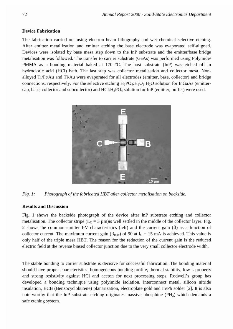
72 Annual Report 2000 - Solid-State Electronics Department
Device Fabrication
The fabrication carried out using electron beam lithography and wet chemical selective etching. After emitter metallization and emitter etching the base electrode was evaporated self-aligned. Devices were isolated by base mesa step down to the InP substrate and the emitter/base bridge metalisation was followed. The transfer to carrier substrate (GaAs) was performed using Polymide/ PMMA as a bonding material baked at 170 °C. The host substrate (InP) was etched off in hydrocloric acid (HCl) bath. The last step was collector metalisation and collector mesa. Non-alloyed Ti/Pt/Au and Ti/Au were evaporated for all electrodes (emitter, base, collector) and bridge connections, respectively. For the selective etching H3PO4:H2O2:H2O solution for InGaAs (emitter-cap, base, collector and subcollector) and HCl:H3PO4 solution for InP (emitter, buffer) were used.
Fig. 1: Photograph of the fabricated HBT after collector metalisation on backside. Results and Discussion
Fig. 1 shows the backside photograph of the device after InP substrate etching and collector metalisation. The collector stripe (LC = 3 µm)is well settled in the middle of the collector layer. Fig. 2 shows the common emitter I-V characteristics (left) and the current gain (β) as a function of collector current. The maximum current gain (βmax) of 90 at IC = 15 mA is achieved. This value is only half of the triple mesa HBT. The reason for the reduction of the current gain is the reduced electric field at the reverse biased collector junction due to the very small collector electrode width.
The stable bonding to carrier substrate is decisive for successful fabrication. The bonding material should have proper characteristics: homogeneous bonding profile, thermal stability, low-k property and strong resistivity against HCl and aceton for next processing steps. Rodwell’s group has developed a bonding technique using polyimide isolation, interconnect metal, silicon nitride insulation, BCB (Benzocyclobutene) planarization, electroplate gold and In/Pb solder [2]. It is also note-worthy that the InP substrate etching originates massive phosphine (PH3) which demands a safe etching system.
E
E
BC
10 µm

Annual Report 2000 - Solid-State Electronics Department 73
1E-5 1E-4 1E-3 0.010
20
40
60
80
100
120
cu
rre
nt
ga
in
IC (A)
Fig. 2: Common emitter I-V characteristics (left) and current gain (β) of the fabricated transferred substrate HBT (AE = 2x10 µm2).
Conclusion
In this work we have investigated and realized the transferred substrate technique for the InP/InGaAs HBT grown by LP-MOVPE. The fabricated HBT shows good dc characteristics with the maximum current gain of about 90. This technique is still under development for better bonding quality and high frequency measurements.
References
[1] Y. Miyamoto, J. M. M. Rios, A. G. Dentai, and S. Chandrasekhar
"Reduction of Base-Collector Capacitance by Undercutting the Collector and Subcollector in GaInAs/InP DHBT’s", IEEE-EDL, Vol. 17, No. 3, March 1996
[2] Q. Lee, S. C. Martin, D. Mensa, R. P. Smith, J. Guthrie, and M. J. W. Rodwell
"Submicron Transferred-Substrate HBTs", Electron Devices Letters 20, No. 8, August 1999
[3] Yutaka Matsuoka, Shoji Yamahata, Kenji Kurishima and Hiroshi Ito
"Ultrahigh-Speed InP/InGaAs DHBT and Analyses of Their Operation", Jpn. J. Appl. Phys. Vol. 35 (1996) pp. 5646-5654, No. 11. November 1996
0.0 0.2 0.4 0.6 0.8 1.0 1.20.0
1.0m
2.0m
3.0m
4.0m
5.0m
6.0m
7.0mIB = 5 µA/step
I C (
A)
V CB (V)

74 Annual Report 2000 - Solid-State Electronics Department
4.3.3 Frequency Dividers using Gates with Non-Linear Negative Feedback
Scientist: A. Brennemann, J. Degenhardt, H. van Husen
Introduction
For optoelectronic communication systems up to 40 Gb/s the InP-based heterostructure field effect transistor (HFET) is often used due to its excellent high frequency performance. To improve the performance of optoelectronic receiver chips a combination of the detection and amplification of the optical signal and the digital preprocessing of the digital data is desired. So logic circuitry capable of highest data rates has to be developed.
For this purpose a non-linear negative feedback (NNFB) was implemented in buffered FET logic (BFL) gates (fig.1). Simulations have shown, that the additional transistor reduces the logic swing of the gate and thus enhances the switching speed without excessive degradation of noise margin. An improvement in the propagation delay of the gate from 21.2 ps to 13.4 ps at a gate length of 0.5 µm was shown. The 11-stage ring oscillator was realized and an oscillation frequency of 3.36 GHz was measured, which corresponds to a propagation delay time of 13.5 ps.
Fig. 1: NOR-gate in buffered FET logic with non-linear negative feedback
Design and Simulation
Another key issue beside switching speed is the compatibility of input and output levels of a logic gate. In the ring oscillator only inverters are used and the requirements for the level compatibility are rather low. But with two or even three input terminals it becomes more and more important to have definite reliable output levels. For example the output low level might depend on the number of inputs in the HIGH-state. To prove the compatibility we have chosen two frequency dividers.

Annual Report 2000 - Solid-State Electronics Department 75
The first one uses two D-flip-flops with a feedback loop of the negative output of the second to the input of the first D-FF (fig. 2a). In each D-FF there are feedback loops between both NOR-gates at the output. The second frequency divider uses even three crossed feedback loops, one of the crossed feedback loops contains a NOR-gate with three inputs (fig.2b). This means a hard demand for the
Fig. 2: a) Frequency divider with 2 D-Flip-flops, b) Frequency divider with 6 NOR-Gates Simulations have shown, that the frequency dividers should work up to an input frequency of fin = 8.3 GHz. Although the second type of frequency dividers consists of much less gates there is no significant difference in the working speed.
IN
OUT
Fig. 3: Micrograph of the frequency divider with 6 NOR-Gates Device fabrication
The circuits were fabricated by using electron beam lithography. The mesa etching was carried out using a negative e-beam resist and a phosphoric based etchant. A single layer PMMA resist (950k, 6% solids) was used for the main patterning steps. The ohmic contacts (Ni/Ge/Au) were annealed at T = 300°C for 5 min, achieving a contact resistance of less than 0.1 Ωmm. The 0.5 µm gates are
>1
>1
>1
>1
>1
>1
>1
>1
1
OUTIN
a)
>1
>1
>1
>1
>1
>1
OUTIN
b)

76 Annual Report 2000 - Solid-State Electronics Department
processed with the identical single layer PMMA process. Subsequently, gate recess is performed using a succinic acid based etchant. For the gate-metalisation and the interconnections of the circuit an Pt/Ti/Pt/Au-metalisation is used.
A drain current of ID = 550 mA/mm and a threshold voltage of VT = -0.6 V were measured. From rf-measurements a cut-off frequency and a maximum frequency of oscillation of fT = 51 GHz and fmax = 132 GHz were evaluated, respectively, for the HFETs used.
Results
The samples were measured within a high speed time domain measurement set-up in an 50 Ω environment (see chap. 4.2.8). The supply voltages were VDD = 2 V and VSS = -2V. The functionality of both types of frequency dividers could be proven in the frequency range from 100 MHz to 3 GHz (fig. 4). The frequency range was restricted by the signal generator at the input. The difference between the input and the output voltages is due to the buffer at the output.
-0.4
-0.2
0
0.2
0.4
0.6
0.8
1
1.2
0 2.00E-09 4.00E-09 6.00E-09
time / s
inp
ut
and
ou
tpu
t vo
ltag
e / V
input output
Fig. 4: Input and output voltage of a frequency divider versus time So these circuits show the capability of the circuits with non-linear negative feedback for high speed digital application e. g. in optoelectronic receiver modules.
References
[1] A. Brennemann, E. Bushehri, M. Agethen, R. M. Bertenburg, W. Brockerhoff, V. Staroselsky, V. Bratov, T. Schlichter, F.-J. Tegude "An 11-Stage Ring Oscillator with Non-linear Negative Feedback for High Speed Digital Applications" Proceeding of the 12th Conference on InP and Related Materials 2000, Williamsburg VA
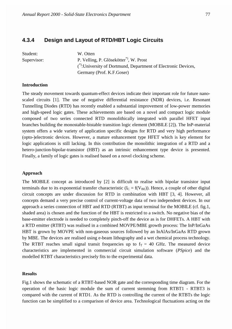
Annual Report 2000 - Solid-State Electronics Department 77
4.3.4 Design and Layout of RTD/HBT Logic Circuits
Student: W. Otten Supervisor: P. Velling, P. Glösekötter*), W. Prost (*):University of Dortmund, Department of Electronic Devices,
Germany (Prof. K.F.Goser) Introduction
The steady movement towards quantum-effect devices indicate their important role for future nano-scaled circuits [1]. The use of negative differential resistance (NDR) devices, i.e. Resonant Tunnelling Diodes (RTD) has recently enabled a substantial improvement of low-power memories and high-speed logic gates. These achievements are based on a novel and compact logic module composed of two series connected RTD monolithically integrated with parallel HFET input branches building the monostable-bistable transition logic element (MOBILE [2]). The InP-material system offers a wide variety of application specific designs for RTD and very high performance (opto-)electronic devices. However, a mature enhancement type HFET which is key element for logic applications is still lacking. In this contribution the monolithic integration of a RTD and a hetero-junction-bipolar-transistor (HBT) as an intrinsic enhancement type device is presented. Finally, a family of logic gates is realised based on a novel clocking scheme.
Approach
The MOBILE concept as introduced by [2] is difficult to realise with bipolar transistor input terminals due to its exponential transfer characteristic (IC = f(VBE)). Hence, a couple of other digital circuit concepts are under discussion for RTD in combination with HBT [3, 4]. However, all concepts demand a very precise control of current-voltage data of two independent devices. In our approach a series connection of HBT and RTD (RTBT) as input terminal for the MOBILE (cf. fig.1, shaded area) is chosen and the function of the HBT is restricted to a switch. No negative bias of the base-emitter electrode is needed to completely pinch-off the device as is for DHFETs. A HBT with a RTD emitter (RTBT) was realised in a combined MOVPE/MBE growth process: The InP/InGaAs HBT is grown by MOVPE with non-gaseous sources followed by an InAlAs/InGaAs RTD grown by MBE. The devices are realised using e-beam lithography and a wet chemical process technology. The RTBT reaches small signal transit frequencies up to fT = 40 GHz. The measured device characteristics are implemented in commercial circuit simulation software (PSpice) and the modelled RTBT characteristics precisely fits to the experimental data.
Results
Fig.1 shows the schematic of a RTBT-based NOR gate and the corresponding time diagram. For the operation of the basic logic module the sum of current stemming from RTBT1 - RTBT3 is compared with the current of RTD1. As the RTD is controlling the current of the RTBTs the logic function can be simplified to a comparison of device area. Technological fluctuations acting on the

78 Annual Report 2000 - Solid-State Electronics Department
current are ruled out because they influence all RTD areas in the same manner. By exploiting the RTBT characteristics in an emitter-follower configuration the transistor does not enter the saturation mode. RTBT2 and RTBT3 are responsible for the inputs a and b (data) and the input of RTBT1 is in charge of the evaluation phase (clk). Due to the fact that the area of each input RTBT is smaller than the area of RTD1 no single input at logic high level can force the MOBILE to latch. Further the sum of the areas of RTBT2 and RTBT3 is smaller than the area of RTD1. Only the combination of clk and one (or two) data(s) at logic high level exceeds the peak current of RTD1 and the MOBILE latches after bistabile-to-monostable transition to high level at its output voltage VMP. The MOBILE is locked in this state until clk or data return to logic low level.
a b
c
Fig. 1: Design (a), SEM micrograph (b), and Spice simulated (c) and low-frequency meansured (d)
timing diagram of a NOR-Gate in MOBILE configuration. Nominally A = 1 corresponds to 30
µm². The output inversion for the measured timing diagram is not shown.
Vext
0 2 4 6 8 t / ns
Vclk
Va
Vb
VMP
0
0
0
1
0
1
0
1
1
0
1
1
d

Annual Report 2000 - Solid-State Electronics Department 79
clk a b
RT
BT
1
out -out Vref
Vext
Rext Vee
Vee2
-clk
RT
BT
2
RT
BT
3
RT
BT
4
HB
T3
HB
T1
HB
T2
HBT4 HBT5
A=
1
A=
1
A=
1
A=
1
A=
1
A=
1
extern
RTD1 RTD2
RTD3 RTD4
A=1,5 A=1,5
Fig.2 shows the design of a RTBT-based multiplexer. Each input branch is based on a RTBT-based gate. Applying logic high level to clk input will activate the corresponding channel meanwhile the other channel is disabled. The output consists out of two HBTs that join the same resonant tunnelling structure in their emitter branch. The functionality of the multiplexer is proven by low frequency measurement and high frequency simulation.
Fig. 2: Design of a 2:1-Multiplexer in MOBILE configuration (left) with output stage (right).
The peak currents of the devices are scaled by the ratio of their area A. Nominally A=1 corresponds to 30 µm² .
Summary:
The InP based HBT in a three-dimensional monolithic integration forming together with the RTD a RTBT is used as the input terminal in the MOBILE logic module. Novel NOR Boolean logic Gate and a multiplexer are designed, realised and tested based on the RTBT device and the MOBILE concept using a novel clocking scheme. SPICE simulation based on measured single device characteristics indicate that the designs allow multi Gb/s operation with robust logic levels. The designs discussed above are now taken into account for the designs of more complex logic circuits.
References:
[1] M.S. Montemerlo, J.C. Love, G.J. Opiteck, J.C. Ellenbogen: “Overview of Nanoelectronic Devices”, Proceedings of the IEEE, volume 85, pp 521-540 (1997).
[2] K.J. Chen, T. Akeyoshi, K. Maezawa: ”Monolithic integration of resonant tunnelling diodes and FET's for monostable-bistable transition logic elements (MOBILE's)“, IEEE Electron Device Letters, volume 16, no. 2, p. 70 (1995).
[3] P. Mazumder und S. Kulkarni, M. Bhattacharya, J.P. Sun, G.I. Haddad: “Digital Circuit Applications of Resonant Tunnelling Devices“, Proceedings of the IEEE, volume 86, no. 4, pp 664-686 (1998).
[4] A. Seabaugh, A. Taddiken, E. Beam III, J. Randall, Y. Kao, B. Newell: “Co-Integrated Resonant Tunnelling Heterojunction Bipolar Transistor Full Adder”, Proceedings of the International Electron Device Meeting, pp 419-422 (1993).

80 Annual Report 2000 - Solid-State Electronics Department
4.3.5 A Depth-2 Full-Adder Circuit using the InP RTD/HFET MOBILE
Scientist: U.Auer, W.Prost, J.Degenhardt, A.Brennemann in collaboration with: C.Pacha
University of Dortmund, Department of Electronic Devices, Germany (Prof. K.F.Goser)
Introduction
Negative-differential resistance devices and circuit architectures based on the monostable-bistable transition logic element (MOBILE [1]) are promising candidates for future high-speed low-voltage digital systems. Recent progress in the manufacturability of Resonant Tunnelling Diodes (RTD) (e.g. [2]) has initiated the design, layout, and technological realisation of more complex structures. In this contribution we will report on depth-2 full-adder circuit using the RTD/HFET MOBILE concept. The demonstrator circuit is a one-bit full adder on InP-substrate.
Design:
Addition is the most frequently used operation in general purpose computing and application specific circuits for digital signal processing (e.g. digital filters). Therefore, the design of an efficient adder is essential for every emerging technology. To obtain a full adder function three digital signals (ai , bi, ci-1) ∈ 0, 1, that are the operands of bit position i (ai, bi) and the carry from the previous position ci-1 are added to compute the sum si and the carry ci-1. In fig.1 a pipelined full adder circuit is presented. To exploit the properties of resonant tunnelling devices a threshold logic style has been chosen so that the addition is performed by:
ci = signai + bi + ci-1 - 2, (1st stage) si = signai + bi + ci-1 - 2ci - 1 (2nd stage)
The arrangement of the adder in a depth-2 circuit composed of two gates is the most compact way to implement a full adder. The evaluation of the logic input signals is initiated by the rising clock edges of VCLK1, and VCLK2. To ensure a correct timing, i.e. the activation of the sum gate si after the carry ci is valid, and to obtain a pipelining, a phase shift of two inverter delays between the rising clock edges is used. This corresponds to an overlapping multi-phase clocking scheme, which is implemented on chip by an SBFL-E/D HFET inverter chain.
Layout and Technology:
The layout of the adders has been made with a minimum RTD area of 2 µm² and HFET gate-length of 0,25 µm. The compact realisation of the circuit is demonstrated using the detail of the basic building block (cf. detail in Fig. 1) composed of a RTD and two HFET input terminals in Fig. 2. The RTD anode is connected to the supply voltage by means of a polyimide bridge. The cathode of the RTD and the out terminal of the building block are drain and source of a dual gate HFET where

Annual Report 2000 - Solid-State Electronics Department 81
one gate is for the clock and the 2nd gate for the data. The supply voltage for this circuit is as low as VDD = 0.7 V.
Epitaxial layers are grown on s.i. InP:Fe substrate in a single MBE run such that the RTD layer is staggered on top of the HFET. Device fabrication is done using direct write e-beam lithography and all wet chemical etching. The device processing started with the evaporation of the RTD anode metal which also serves as a mask for the following etch step forming the RTD's. In a second etch step the HFET-mesas are defined while the RTD interconnection fingers are under-etched. After the evaporation and alloying of the HFET-source and drain contacts the depletion-type gates are fabricated. Polyimide is patterned for the following final metal step completing the connection of the circuit and forming the enhancement-type gates. The effective RTD anode area is less than 2 µm² leading to a peak current of 0.40 mA per input stage. The extrinsic transconductance of the HFET is 510 mS/mm.
8
8
8
8
14 8
8
8
8
8
8
1412
22 5 222 54
ai
bi
ci-1
si
12
VDD1
VCLK
VDD1
GND
8 8
GNDGND
VDD1
GND
1st stagecarry
2
8
8
basic module
VDD2 VDD2
ci
2nd stagesum
clock delay clock delay
Fig.1: Design of a Depth-2 One-bit Pipelined Threshold Logic Full Adder with local clock generation and delay by an E/D HFET Super-Buffer inverter chain. The "basic module" of a series connection of a RTD-HFET-HFET is given in detail in Fig. 2. The numbers at the devices indicate RTD area in [µm²] or HFET gate width [µm].
Evaluation and Comparison
The performance of the adder in terms of circuit delay, output rise times, and power dissipation, is evaluated using SPICE simulation (Table I). The operation of the circuit and has been verified for fclk=1 GHz considering all possible logic input combinations. Using an optimised clocking scheme and scaled devices with higher peak current density the clock frequency can be increased about 20 GHz.

82 Annual Report 2000 - Solid-State Electronics Department
a
RTD anode
mesa
ohm contact(Drain)
clockpolyimide bridge
data ohm contact(Out, Source)
VDD
5 µm
b
Fig.2: Layout (a) and SEM microgaph (b) of a RTD-HFET-HFET input stage module of the threshold logic full adder composed of a self-aligned directly contacted RTD and 0,25 µm gate length HFET gates of the clock and input transistor. The VDD –line is leaded on polyimide bridges over the gates.
Table I: Simulated performance and specifications of the pipelined full adder
(VDD=0.7V and fCLK=1 GHz)
Logic level: high VH=0.63 V low VL=0.08 V
Power dissipation: Average Pave=725 µW Maximum Pmax=1.55 mW
Output rise times: carry tr(ci)=250 ps, sum tr(si)=145 ps
Delay: output td(ci)=144 ps, td(si)=270 ps Clock Phase tCC=145 ps
Circuit Area: 65 µm x 35 µm
Acknowledgment:
The work is funded by the European project LOCOM within the Future and Emerging Technologies, Nanoscale Information Devices Cluster
References: [1] K. Chen, K. Meazawa, M. Yamamoto: InP Based High Performance Monostable-Bistable
Transition Logic Elements (MOBILE’s) Using Integrated Multiple-Input Resonant-Tunnelling Devices, IEEE Electron Dev. Lett., Vol. 17, No. 3, March 1996, pp. 127-129.
[2] W.Prost, U.Auer, F.-J.Tegude, C.Pacha, K.F.Goser, G.Janßen, T. van der Roer; Manufacturability and Robust Design of Nanoelectronic Logic Circuits based on Resonant Tunnelling Diodes, J. Circuit Theory and Applications, Special Issue on Nanoelectronic Circuits 2000; 28, 537-552

Annual Report 2000 - Solid-State Electronics Department 83
4.3.6 Low-voltage MOBILE Logic Module Based on Si/SiGe Interband Tunnelling Diodes
Scientist: U. Auer, M. Agethen, W. Prost, in collaboration with: R. Duschl, K. Eberl Max-Planck-Institut für Festkörperforschung, Stuttgart, Germany Introduction
Negative-differential resistance (NDR) devices in combination with high-speed transistors are well suited for a robust dual valued logic [1-2]. The NDR effect is provided by interband-tunnelling (ITD) or resonant tunnelling diodes (RTD), respectively. III/V-RTD's have provided very high speed [2], and robust [3] logic functions based on the monostable-bistable transition logic element (MOBILE) [1]. In addition, novel circuit architectures allow a reduced complexity for computational circuits [2]. In this contribution we will demonstrate and analyse high speed Si/SiGe-ITD's on high resistivity n--Si-substrates. A MOBILE latch is built and its logic operation is demonstrated at a very low bias.
Technology of High-Speed Si/SiGe-ITD
Si/SiGe-ITD's were grown by molecular beam epitaxy (MBE) on high resistivity n--Si-substrates [for details refer to 3] at Max-Planck-Institut für Festkörperforschung, Stuttgart, Germany. The layer structures were optimised with respect to a low-voltage logic. The embedded SiGe-interlayer in the intrinsic zone increases the PVCR. A Ge-content of 48% is chosen resulting in a maximum thickness of 3 nm for the pseudomorphic growth. In addition, a post growth high temperature annealing sequence is necessary for high performance devices [3].
a
a-8 -4 0 -4
depth (z-z0) / nm
Si0.52Ge0.48
8
p-regionn-region
(n++)
(p++)
EC
EV
ener
gy (
E-E
0) /
eV
0.0
-0.5
-1.0
0.5
b
Fig. 1: Band structure (a) and SEM micrograph of the 1-metal diode (b) of a Si/SiGe ITD. The fabrication of the planar 1-metal ITD starts with the evaporation of Ti/Pt/Au serving simultaneously as the anode and cathode metal contact (cf. fig.1). The structure was etched down to the p+-buffer in order to isolate anode and cathode. A final etch step removes the p-doped buffer and isolates the contact pads by underetching the anode-interconnection finger. The sample S1393 shows a peak voltage VPeak of 110 mV, a peak current density of JPeak = 0.52 kA/cm² and a PVCR of 2.1. Further experiments showed that the peak current density may be increased up to JPeak =

84 Annual Report 2000 - Solid-State Electronics Department
17.1 kA/cm² without a decrease of PVCR = 2.6 but to the expense of a 3 times higher peak voltage (VPeak = 296 mV).
Si/SiGe-ITD gate
A MOBILE type logic gate is formed by the series connection of two identical ITD's (cf. inlet Fig. 2). The logic function of the gate is obtained by applying a dynamic clock voltage Vclk over the gate and measuring the output voltage for different input currents Iin into the common node (bifurcation curve, c.f. Fig. 2). The input current Iin will be provided finally by a transistor either parallel to the driver ITD corresponding to Iin < 0 or to the load ITD corresponding to Iin > 0. A robust switching operation of the gate is realised by means of an input current of ± 50 µA resulting in an almost perfect voltage swing ∆V = VH – VL of 81 % of the applied clock voltage.
0 0.2 0.4 0.6 0.8 1
clock voltage Vclk (V)
0
0.2
0.4
0.6
outp
ut v
olta
ge V
out (
V)
Iin = +50 AIin = +50
Iin = - 50 AIin = - 50 P
P
S1393
load
Iin Vout
Vclk
VH
VL
driver
Fig. 2: Bifurcation curve of two series connected ITD demonstrating the MOBILE function with
a switching current of ± 50 µA.
Using a HP8510C network analyser, the high frequency performance of the Si/SiGe-ITD has been measured from 45 MHz to 40 GHz. The small-signal elements of an equivalent circuit model of the ITD (inlet in Fig. 3) have been extracted using an optimisation algorithm based on the simulated evolution. The mean square deviation between simulated and measured S-parameters was less than 5%. The intrinsic ITD device is given by the parallel capacitance CP and the conductance gP. Fig. 3 shows the bias dependence of the intrinsic device consisting of the parallel capacitance CP and conductance gP. The conductance gP representing the frequency range 45 MHz to 40 GHz is in good agreement with the deduced DC differential input conductivity ∆IDC/∆VDC. A steady increase of the device capacitance CP from 620 fF to 1040 fF with increasing bias is modelled. Using the data form the intrinsic device the switching speed can be estimated using the speed-index s:
,P
P
I
C
V
ts =
∆∆= (1)
which corresponds to the charging time of the device capacitance CP with the peak current IP . The parameter CP of eq. 1 can be approximated (cf. Fig. 3) to an average value of 680 fF while the peak current is 0.31 mA. The data result in a speed-index s = 2.2 ns/V which corresponds to 0.53 ns for changing the output from the low level VL to the high level VH. The ITD data given above are

Annual Report 2000 - Solid-State Electronics Department 85
deduced from a device with 60 µm² anode area. Higher frequencies will be possible using higher current density ITD's at reduced device area (1 µm²).
S1393
31 fF CP gP
126 pH 29 Ω
0.8 pF
120
Ω
0 0.1 0.2 0.3 0.4 0.5 0.6voltage (V)
600
700
800
900
1000
1100
capa
cita
nce
Cp (
fF)
-1
0
1
2
3
4
5
cond
ucta
nce
g p (
mS
)
CpCp
gpgp
A = 60 mm2A = 60 Pm2
500
∆IDC
∆VDC=
Fig. 3: Voltage dependent ITD small signal parameter capacitance CP and conductance gP
extracted from the best fit to the measured S-parameter using a small-signal equivalent circuit as given in the inlet. For comparison the differential input conductivity ∆IDC/∆VDC of the device is given.
Conclusions
A logic gate composed of two series connected Si/SiGe ITD's according to the MOBILE principle is realised. A high voltage swing of 81% of the clock voltage is obtained at a bias as low as 0.3 V. A speed analysis revealed a speed index of 2.2 ns/V which corresponds to on/off switching time of 0.5 ns. Monolithic combinations of these ITD's with three-terminal devices (Si/SiGe based HBT or HFET) may form low-voltage logic modules for future high speed mobile communication systems.
Acknowledgements: The work was partly funded by the European Union under contract LOCOM within the Future and Emerging Technolgoies, Nanoscale Information Devices cluster. References:
[1] K. Chen, K. Maezawa, M. Yamamoto, "InP Based High Performance Monostable-Bistable Transition Logic Elements (MOBILE’s) Using Integrated Multiple-Input Resonant-Tunnelling Devices", IEEE Electron Device Lett., vol. 17, pp. 127-129, 1996.
[2] C. Pacha, U. Auer, C. Burwick, P. Glösekötter, A. Brennemann, W. Prost, F.-J. Tegude, K. F. Goser, "Threshold Logic Circuit Design of Parallel Adders Using Resonant Tunnelling Devices", IEEE Transactions on Very Large Scale Integration Systems, vol. 8, no. 5, pp.558-572, 2000.
[3] R. Duschl, O. G. Schmidt, K. Eberl, "Epitaxially grown Si/SiGe interband tunneling diodes with high room-temperature peak-to-valley ratio", Applied Physics Letters, vol. 76, pp. 879-881 (2000).

86 Annual Report 2000 - Solid-State Electronics Department
4.3.7 Combining HBT and EAM for 1.55µm to a Merged Device
Scientists: T. Reimann, P. Velling, S. Neumann, M. Agethen, R.M. Bertenburg in collaboration with: M. Schneider, R. Heinzelmann, A. Stöhr (Duisburg University, Dept.
of Optoelectronics, Prof. D. Jäger)) Technician: M. Haase
Introduction
There is a continuous development in the monolithic integration of electronic and optical devices to add functionality and improve performance. Here we focus on the combination of heterostructure bipolar transistors (HBTs) and electroabsorption waveguide modulators (EAMs). One way is to stack the two layer structures for each device on top of each other [1], resulting in two separate devices, which have to be processed one after the other. A different possibility is to integrate the waveguide modulator into the collector region of the HBT. Similar was done with a waveguide switch in combination with a HBT [2]. In our approach we choose to take the modulator inside the collector and employ mainly the voltage swings between the base and collector, which change the electric field and therefore the band edge due to the Franz-Keldysh effect (FKE). Additionally, the collector current influences the band gap due to band-filling. The resulting layer stack enables a new type of merged device (HBT-EAM). This corresponds to a modulator with an integrated amplifier and therefore the demands on a driver circuit can be reduced. Additionally, optical waveguides, modulators and bipolar transistors can be processed as single devices from the same layer.
If the HBT of the merged device is operated in the common-emitter configuration with load resistance it is able to switch the build-in EAM (fig.1). When the transistor is in off-state, the base-collector diode is reversely biased, which results in a high electric field inside the collector, i.e. in the region of the optical waveguide, thus the optical power is absorbed.
EAM
RL
IB
VCCVCB IC
n+-In0.53Ga0.47Asn = 1×1019 cm-3
n-InPn = 5×1017 cm-3
p+-In0.53Ga0.47Asp = 1.3×1019 cm-3
Emitter-Cap140 nm
Emitter60nmBase
75 nm(i) In0.53Ga0.47As Step grading 30 nm
(i) InP
n+-InPn = 5×1018 cm-3
InP-Substrate
Sub-Collector +Cladding
250 nm
Collector + Cladding450 nm
Collector + Guide420 nm
(i) In0.62Ga0.38As0.82P0.18
(i) InP Buffer 50nm
λg = 1.48 µm
EA
M
HB
T
E
Fig. 1: HBT-EAM in common-emitter Fig. 2: Multifunctional layer stack, which configuration. combines HBT and EAM.
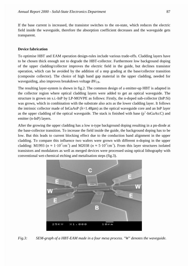
Annual Report 2000 - Solid-State Electronics Department 87
If the base current is increased, the transistor switches to the on-state, which reduces the electric field inside the waveguide, therefore the absorption coefficient decreases and the waveguide gets transparent.
Device fabrication
To optimise HBT and EAM operation design-rules include various trade-offs. Cladding layers have to be chosen thick enough not to degrade the HBT-collector. Furthermore low background doping of the upper cladding/collector improves the electric field in the guide, but declines transistor operation, which can be avoided by the addition of a step grading at the base/collector transition (composite collector). The choice of high band gap material in the upper cladding, needed for waveguiding, also improves breakdown voltage BVCB.
The resulting layer-system is shown in fig.2. The common design of a emitter-up HBT is adapted in the collector region where optical cladding layers were added to get an optical waveguide. The structure is grown on s.i.-InP by LP-MOVPE as follows: Firstly, the n-doped sub-collector (InP:Si) was grown, which in combination with the substrate also acts as the lower cladding layer. It follows the intrinsic collector made of InGaAsP (λ=1.48µm) as the optical waveguide core and an InP layer as the upper cladding of the optical waveguide. The stack is finished with base (p+-InGaAs:C) and emitter (n-InP) layers.
After the growing the upper cladding has a low n-type background doping resulting in a pn-diode at the base-collector transition. To increase the field inside the guide, the background doping has to be low. But this leads to current blocking effect due to the conduction band alignment in the upper cladding. To compare this influence two wafers were grown with different n-doping in the upper cladding: M1993 (n ≈ 1·1017cm-3) and M2038 (n ≈ 5·1015cm-3). From this layer structures isolated transistors and modulators as well as merged devices were processed using optical lithography with conventional wet-chemical etching and metalisation steps (fig.3).
Fig.3: SEM-graph of a HBT-EAM made in a four mesa process. "W" denotes the waveguide.

88 Annual Report 2000 - Solid-State Electronics Department
0 1 2 3 4 5 60123456789
101112131415
M1993E
M2038A
I B =
5µ
A/S
tepBmax=150
40µ A
A tot = 8*50 µ m2 (A E=116µ m
2)
Bm ax=140
80µ A
I B =
10
µA
/Ste
p
I C (
mA
)
VCE (V)0 2 4 6 8 10
0.0
0.5
1.0
1.5
2.0
2.5
3.0
3.5
4.0
4.5
M2038A R L=22kΩ
HM11 A to t=16*50 µ m2
Laser: 1580.0 nm, 1.0 mWswitch from IB=6 µA to
IB=-2.0 µA
IB=-1.0 µA
IB= 0.0 µA
IB= 1.0 µA
IB= 2.0 µA
IB= 3.0 µA
IB= 5.0 µA
op
tica
l co
ntr
ast
(d
B)
VCC (V)
Fig.4: DC output characteristics of Fig.5: Optical contrast of a HBT-EAM in two HBT-EAMs (see text). common-emitter configuration.
Measurements
The merged devices (HBT-EAMs) can be used also as pure HBTs. For two exemplary devices the common-emitter characteristics are recorded (fig.4). They differ in the background doping of the upper cladding as mentioned. As can be seen the HBT-EAM with the higher doping in the collector (fig.4, wafer M1993) has a lower turn-on voltage (less current blocking), but the corresponding EAMs need higher voltage swings for the same optical modulation, as expected. RF-measurements taken from the HBT-EAM (M2038) show fT = 23GHz and fmax = 20GHz. For M1993 the values are similar fT = 24GHz and fmax = 25GHz.
Optoelectronic DC-measurements of a HBT-EAM (in common-emitter configuration) are illustrated in fig.5. A tuneable laser source is connected to the HBT-EAM by a tapered single-mode fiber. At the opposite side of the device a cleaved single-mode fiber picks up the guided and modulated mode and gives it to an optical powermeter. The device achieves an optical contrast of more than 4dB at a base current switched from 6µA to -2µA at VCC=10V. Negative base currents are needed to switch off the transistor completely due to absorption of light. Additionally mesa waveguide modulators (EAM's) with 200µm length and 9µm width exhibit a 3dB cut-off frequency of 10GHz (at 1.55µm).
The next step is to provide a suitable RF-measurement environment with an on-chip load resistor. This will lead to applications, where HBT-EAMs are combined with other electric devices.
References: [1] M.T. Camargo Silva, J.E. Zucker, L.R. Carrion, C.H. Joyner, A.G. Dentai, "Growth
Optimization for p-n Junction Placement in the Integration of Heterojunction Bipolar Transistors and Quantum Well Modulators on InP", IEEE J. Selected Topics in Quantum Electron., vol 6, p. 26, 2000.
[2] N. Shaw, P.J. Topham, M.J. Wale, "Optical switches and heterojunction bipolar transistors in InP for monolithic integration", ESSDERC '90, p. 551, 1990.

Annual Report 2000 - Solid-State Electronics Department 89
4.3.8 Laterally Controlled Deposition of Nanoparticles for Microelectronic
Scientists: F. Otten, in collaboration with: E. Kruis, H. Fissan (Dept. of Process- and Aerosol Technology, Prof. H. Fißan) Quantum devices have minimum feature sizes of a few nanometers. Producing small structures (d< 50 nm) by high resolution lithography reaches the economical and physical limits. The use of simpler nanopatterning techniques result in loss of structure control and engineering design. The goal of this research project is to implement the gas-phase synthesis of nanostructures into microelectronic technology to fulfill the design control. Figure 1 shows the schematic of the nanoparticle synthesis set-up.
Fig.1: Experimental set-up for the synthesis, size fractionation, sintering and deposition of PbS nanoparticles. The synthesis takes place at atmospheric pressure in an inert atmosphere.
Lead sulfide (PbS) powder is evaporated in a tube furnace at ambient pressure and nitrogen gas flow. After cooling nanoparticles are formed from the supersaturated gas. The nanoparticles are charged in a neutralizer and size selected in a differential mobility analyser, followed by a reheating process for compaction and crystallization of the nanoparticles. Finally the nanoparticles are deposited in an electrostatic precipitator forming thin films onto test substrates. [1]
Electrostatic lenses formed by charged and patterned photoresist are employed to control the deposition process of the nanoparticles. This technique is a parallel process and has therefore a big advantage compared to serial pattern definition e.g. by electron beam lithography [2]. In fig.2a) the scheme of the processing steps and in b) the electric field of the electrostatic lenses are depicted.
PbS nanoparticles are since PbS already exhibits quantization effects at feature sizes at about 20 nm [3] and PbS nanoparticle films can be patterned by standard lithography. First results of the focusing effect of photoresist is shown in fig.3. Nanoparticles are focused into the windows where the n-doped GaAs substrate is not covered by photoresist. The deposition area width of the nanoparticle

90 Annual Report 2000 - Solid-State Electronics Department
film is smaller than the employed photoresist pattern as shown in fig.3. This offers the possibility to create chains of nanoparticles with a width of a few nanoparticle diameters. A simulation of the electrostatic field of patterned and charged photoresist is shown in figure 2 b). The strong lateral electric field explains the observed focusing effect. The results can be transferred to other materials.
a) b)
Fig.2: Scheme of a) the processing steps to pattern nanoparticle films and b) the electrostatic field of patterned photoresist charged with 500 charges / µm2 simulated with Quickfield®.
Fig.3: SEM pictures of a) thin patterned film and b) thick patterned film of PbS nanoparticles References:
[1] F.E. Kruis, K. Nielsch, H. Fissan, B. Rellinghaus and E.F. Wassermann: Appl. Phys. Lett., 1998, 74, 547.
[2] W. Prost, F.E. Kruis, F. Otten, K. Nielsch, B. Rellinghaus, U. Auer, A. Peled, E.F. Wassermann, H. Fissan and F.J. Tegude, Microelectron. Eng.,1998, 41/42, 535.
[3] Y. Wang and N. Herron: J. Phys. Chem., 1991, 95, 525.
200 kV/µm2

Annual Report 2000 - Solid-State Electronics Department 91
4.4 Conference Contributions
1. A.LESE1), J.SPIELER
1), T.KLIPPENBERG1), P.KIESEL
1), G.H.DÖHLER1), P.VELLING, W.PROST, F.J.TEGUDE
1): Institut für Technische Physik I, Universität Erlangen-Nürnberg, Germany
Auswirkungen unterschiedlicher Wachstumsparameter auf die spontane Ausbildung von Übergitterordnungen DPG Frühjahrstagung, 2000
2. P.VELLING, M.AGETHEN, W.PROST, F.J.TEGUDE
InAlAs/InGaAs/InP Heterostructures for RTD and HBT Device Applications Grown by LP-MOVPE Using Non-Gaseous Sources MOVPE X, Sapporo, Japan, June 2000
3. P.VELLING
InAlAs/InGaAs/InP RTD/HBT device structures grown by LP-MOVPE Using Non-Gaseous Sources: X-Ray Characterization and Device Applications a) Vortrag an der KTH-Schweden, Stockholm am 31 März 2000 b) Vortrag bei NTT Photonics Lab. Japan, Atsugi, 14.06.2000 c) Vortrag bei Hitachi-Cable, Japan, Hitachi, 19.06.2000
4. A.BRENNEMANN, E.BUSHEHRI, M.AGETHEN, R.M.BERTENBURG, W.BROCKERHOFF, V.STAROSELSKY1),
V.BRATOV1), T.SCHLICHTER
1), F.J.TEGUDE 1): Microelectronics Center, Middlesex University, London, U.K.
An 11-Stage Ring Oscillator with Nonlinear Negative Feedback for High Speed Digital Applications '12th Int. Conf. on InP and Related Materials' (IPRM 2000), Williamsburgh, VA, USA, 14.05.-18.05.00
5. S.-O. KIM, P.VELLING, U.AUER, M.AGETHEN, W.PROST, F.J.TEGUDE
High fT, High Current Gain InP/InGaAs:C HBT Grown by LP-MOVPE with Non-Gaseous Sources '12th Int. Conf. on InP and Related Materials' (IPRM 2000), Williamsburgh, VA, USA, 14.05.-18.05.00
6. P.VELLING, M.AGETHEN, W.PROST, F.J.TEGUDE
InAlAs/InGaAs/InP Heterostructures for RTD anfd HBT Device Applications Grown by LP-MOVPE Using Non-Gaseous Sources MOVPE X, Sapporo, Japan, June 2000
7. S.-O.KIM, P.VELLING, M.AGETHEN, TH.REIMANN, W.PROST, F.J.TEGUDE
InP-Based HBT with Garded InGaAlAs Base Layer Grown by LP-MOVPE 'European GaAs and Other Semiconductor Application Symposium'(GaAs 2000), Paris, France, 2-3 October 2000
8. A. BRENNEMANN
Digital Circuits on InP using HFETs and RTD/HFET combinations a) Seminar at the Naval Research Lab, Washington DC, 19.05.2000 b) Seminar at the Department of Electrical Engineering, University of Notre Dame, South Bend, IN, 22.05.2000 c) Seminar at the Microelectronics Center, University of Illinois, Urbana, IL, 24.05.2000

92 Annual Report 2000 - Solid-State Electronics Department
9. T. KIPPENBERG1, J. SPIELER
1, P. KIESEL1, G.H. DÖHLER
1, M. MOSER2, P.VELLING, W. PROST, F. J.
TEGUDE 1: Institute of Technical Physics, University of Erlangen 2: CSEM, Zürich, Switzerland.
Characterization of Spontaneous Ordering in GaInP and InGaAs poster presentation: Tagung der Deutschen Physikalischen Gesellschaft (DPG-Frühjahrstagung), Regensburg, 27-31. März 2000
10. J. SPIELER1; P. VELLING; TH. KIPPENBERG
1; P. KIESEL1; A. LESE
1; M. MÜLLER1; W. PROST; F. J. TEGUDE;
G.H. DÖHLER1
1Friedrich-Alexander University Erlangen-Nürnberg, Institut für Tech. Phys. I, Erlangen D-91058 Germany.
Polarization Dependent Electro-Absorption Measurements - a Powerful Tool to Study Ordering Induced Changes of the Electronic Band Structure of InGaAs 2000 Electronic Materials Conference, Symposium on Ordering in Semiconductor Alloys, Denver, Colorado - USA, Jun - 21 - 23, 2000.
11. W.PROST;
Circuit Applications of Resonant Tunnelling Diodes Université de Provences, Institut Charles Fabry, Marseille, 14.01.2000.
12. W.PROST;
Circuit Applications of Resonant Tunnelling Diodes, Seminar at Universita' di Parma, Febr. 21, 2000.
13. W.PROST, P.VELLING, G.JANSSEN, U.AUER, A.BRENNEMANN, P.GLOSEKÖTTER, K.F.GOSER, F.-J. TEGUDE,
Resonant-Tunnelling 3-Terminal Devices for High-Speed Logic Application, 24th Europ. Workshop on Compound Semiconductor Devices and Integrated Circuits (WOCSDICE), Aegean Sea, Greece, May 29 - June 2, 2000.
14. W.PROST;
III/V-Halbleiterheteroepitaxie und Entwicklung schaltungsrelevanter Resonanztunneldioden, RWTH Aachen, Kolloquium der Fakultät für Elektrotechnik und Informationstechnik, Aachen, 6. Juni, 2000.
15. P. VELLING
Elektronische III/V-Halbleiter Bauelemente Eingeladener Vortrag: Graduierten Kolleg der Philipps Universität Marburg, September 2000
16. P. VELLING, M. AGETHEN, E. HERENDA, W. PROST, W. STOLZ1, F.-J. TEGUDE
1Materials Sciences Center and Department of Physics, Philipps University, Marburg.
LP-MOVPE Growth of Carbon Doped In0.48Ga0.52P/GaAs HBT Using an All-Liquid-Source Configuration '26th Int. Symp. on Compound Semiconductors, Berlin, 22-26 August 1999

Annual Report 2000 - Solid-State Electronics Department 93
17. P. GLÖSEKÖTTER1, C. PACHA
1, K. F. GOSER1, G. I. WIRTH
1, W. PROST, U. AUER, M. AGETHEN, P. VELLING, F. J. TEGUDE 1University of Dortmund, Department of Electronic Devices.
Digital Circuit Design Based on the Resonant-Tunnelling-Hetero-Junction-Bipolar-Transistor 13th Symposium on Integrated Circuits and Systems Design (SBCCI 2000), pp. 150-155, Manaus, Amazonas, Brazilien, published by the IEEE Computer Society, September 2000
18. S. NEUMANN, P. VELLING, S.-O. KIM, M. AGETHEN, W. PROST, F.-J. TEGUDE
InP-based HBT with p-(InGaAl)As:C base grown by LP-MOVPE with non-gaseous sources 12th III/V-Semiconductor Device Simulation Workshop / HBT Workshop, Duisburg, Oct. 2000
19. S.-O. KIM, P. VELLING, M. AGETHEN, S. NEUMANN, W. PROST, F.-J. TEGUDE
Transferred substrate technique for InP/InGaAs HBT 12th III/V-Semiconductor Device Simulation Workshop / HBT Workshop, Duisburg, Oktober 2000.
20. T. REIMANN, M. SCHNEIDER1, P. VELLING, S. NEUMANN, M. AGETHEN, R. M. BERTENBURG, R.
HEINZELMANN1, A. STÖHR
1, D. JÄGER1, F.-J. TEGUDE
HBT combining elektroabsorption waveguide modulator based on a multifunctional layer structure design for 1,55 µm 12th III/V-Semiconductor Device Simulation Workshop / HBT Workshop, Duisburg, Oktober 2000, 1Fachgebiet für Optoelektronik, Universität Duisburg.
21. B. SCHLOTHMANN, R. M. BERTENBURG, M. AGETHEN, P. VELLING, F.-J. TEGUDE
Two-dimensional physical simulations of InP/InGaAs HBT 12th III/V-Semiconductor Device Simulation Workshop / HBT Workshop, Duisburg, Oktober 2000.
22. M. AGETHEN, P. VELLING, W. BROCKERHOFF, F.-J. TEGUDE
Small-signal and rf-modelling of InP/InGaAs HBT 12th III/V-Semiconductor Device Simulation Workshop in combination with HBT Workshop, Duisburg, Oktober 2000.
23. P. VELLING, S. NEUMANN, A. BRENNEMANN, M. AGETHEN, W. PROST UND F.J. TEGUDE
Pseudomorphes InAlP auf InP-Substrat für HFET und RTD Anwendungen gewachsen mittels LP-MOVPE mit nicht gasförmigen Quellen in N2
'15. DGKK-Workshop', Bad Dürkheim, December 2000
24. S. NEUMANN, P. VELLING, J. SPIELER1, A. LESE
1, T. KIPPENBERG1, S-O. KIM, M. AGETHEN, W. PROST, G.
H. DÖHLER1, F.-J. TEGUDE
1Friedrich-Alexander University Erlangen-Nürnberg, Institut für Tech. Phys. I, Germany.
Wachstum und Charakterisierung von geordnetem InGaAs als Spacer in InGaAs/InP HBT-Strukturen '15. DGKK-Workshop', Bad Dürkheim, December 2000
94 Annual Report 2000 - Solid-State Electronics Department
4.5 Publications
1. J.SPIELER1, T.KLIPPENBERG
1, J.KRAUß1, P.KIESEL
1, G.H.DÖHLER1, P.VELLING, W.PROST, F.J.TEGUDE
1: Institut für Technische Physik I, Universität Erlangen-Nürnberg, Germany
Electro-Optical Examination of the Band Structure of Ordered InGaAs Applied Physics Letters, Vol.76, No.1, pp.88-90, January 2000
2. P. VELLING, M. AGETHEN, E. HERENDA, W. PROST, *W. STOLZ, F.-J. TEGUDE
LP-MOVPE Growth of Carbon Doped In0.48Ga0.52P/GaAs HBT Using an All-Liquid-Source Configuration Institute of Physics Conference Series No. 166, Chap.2, 2000, Proc. of '26th Int. Symp. on Compound Semiconductors, Berlin, 22-26 August 1999
3. P.KOPPERSCHMIDT1), KÄSTNER
1), SENZ1), SCHOLZ
1), GÖSELE1), P.VELLING, W.,PROST, F.J.TEGUDE,
GOTTSCHALCH2), WADA
2)
Strain Relaxation during Heteroepitaxy on twist-bounded thin GaAs Substrates 1): Max-Planck Institut, Halle, Germany 2): Universität Leipzig, Germany Materials Research Society, Conf. Series Vol. 535: III-V and IV-IV Materials and Processing Challenges for Highly Integrated Microelectronics and Optoelectronics"
4. A.BRENNEMANN, E.BUSHEHRI, M.AGETHEN, R.M.BERTENBURG, W.BROCKERHOFF, V.STAROSELSKY1),
V.BRATOV1), T.SCHLICHTER
1), F.J.TEGUDE 1): Microelectronics Center, Middlesex University, London, U.K.
An 11-Stage Ring Oscillator with Nonlinear Negative Feedback for High Speed Digital Applications Proc. of '12th Int. Conf. on InP and Related Materials' (IPRM 2000), Williamsburgh, VA, USA, 14.05.-18.05.00
5. S.-O. KIM, P.VELLING, U.AUER, M.AGETHEN, W.PROST, F.J.TEGUDE
High fT, High Current Gain InP/InGaAs:C HBT Grown by LP-MOVPE with Non-Gaseous Sources Proc. of '12th Int. Conf. on InP and Related Materials' (IPRM 2000), Williamsburgh, VA, USA, 14.05.-18.05.00
6. P.VELLING, M.AGETHEN, W.PROST, F.J.TEGUDE
InAlAs/InGaAs/InP Heterostructures for RTD anfd HBT Device Applications Grown by LP-MOVPE Using Non-Gaseous Sources Journal of Crystal Growth, Special Issue of MOVPE X, Sapporo, Japan, June 2000
7. P.VELLING, M.AGETHEN, W.PROST, W.STOLZ, F.J.TEGUDE 1): Materials Sciences Center and Dept. of Physics, Marburg, Germany
A Comparative Study of GaAs- and InP-based HBT Growth by Means of LP-MOVPE Using Conventional and Non Gaseous Sources Special Issue of Journal of Crystal Growth (invited), Dec. 2000,
8. S.-O.KIM, P.VELLING, M.AGETHEN, TH.REIMANN, W.PROST, F.J.TEGUDE
InP-Based HBT with Graded InGaAlAs Base Layer Grown by LP-MOVPE European GaAs and Other Semiconductor Application Symposium (GaAs 2000), Paris, France, 2-3 October 2000

Annual Report 2000 - Solid-State Electronics Department 95
9. W.PROST, P.VELLING, G.JANSSEN, U.AUER, A.BRENNEMANN, P.GLOSEKÖTTER, K.F.GOSER, F.-J. TEGUDE, 1 Universität Dortmund, LS Bauelemente der Elektrotechnik
Resonant-Tunnelling 3-Terminal Devices for High-Speed Logic Application, 24th Europ. Workshop on Compound Semiconductor Devices and Integrated Circuits (WOCSDICE), Aegean Sea, Greece, May 29 - June 2, 2000.
10. W.PROST, U.AUER, F.-J.TEGUDE, C.PACHA, K.F.GOSER, G.JANßEN, T. VAN DER ROER;
Manufacturability and Robust Design of Nanoelectronic Logic Circuits based on Resonant Tunnelling Diodes, Int. J. of Circuit Theory and Applications, Special Issue on Nanoelectronic Circuits, Vol. 28, pp.537-552
11. C.PACHA 1, O.KESSLER
1, K.F.GOSER 1, W.PROST, A.BRENNEMANN, U.AUER, F.-J.TEGUDE;
1 Universität Dortmund, LS Bauelemente der Elektrotechnik
Parallel Adder Design with Reduced Circuit Complexitiy Using Resonant Tunnelling Transistors and Threshold Logic Analog Integrated Circuits and Signal Processing, 24, pp. 7-25, 2000, Kluver Academic Publishers
12. C.PACHA1, U.AUER, C.BURWICK
1, P.GLÖSEKÖTTER1, A.BRENNEMANN, W.PROST, F.-J.TEGUDE,
K.F.GOSER1;
1 Universität Dortmund, LS Bauelemente der Elektrotechnik
Threshold Logic Circuit Design of Parallel Adders Using Resonant Tunnelling Devices IEEE Transactions on Very Large Scale Integration Systems, Vol.8, No.5. Oct. 2000, pp. 558-572
13. D.KEIPER1, P.VELLING, W.PROST, M.AGETHEN, F.J.TEGUDE, G.LANDGREN
1 1: Dept. of Electronics, Royal Institute of Technology (KTH), Electrum 229, Kista, Sweden
Metallorganic Vapour Phase Epitaxy (MOVPE)Growth of InP-Based Heterojunction Transistors (HBT) with Carbon Doped InGaAs Base Using tertiarybutylarsine (TBA), tertiarybutylphosphine (TBP) in N2 Ambient Jap. Journal of Applied Physics, Vol. 39, No.11, Nov. 2000, pp. 6162-6165
14. F.OTTEN, L.B.KISH, C.G.GRANQVIST, L.K.J.VANDAMME, R.VAJTAI, F.E.KRUIS, H.FISSAN
Charge Diffusion Noise in Monocrystalline PbS Nanoparticle Films Applied Physics Lett., Vol. 77 (21), Nov. 2000, pp. 3421-3422
15. P. GLÖSEKÖTTER1, C. PACHA
1, K. F. GOSER1, G. I. WIRTH
1, W. PROST, U. AUER, M. AGETHEN, P. VELLING, F. J. TEGUDE: 1University of Dortmund, Department of Electronic Devices
Digital Circuit Design Based on the Resonant-Tunnelling-Hetero-Junction-Bipolar-Transistor Proc.: 13th Symposium on Integrated Circuits and Systems Design (SBCCI 2000), pp. 150-155, Manaus, Amazonas, Brazilien and IEEE Computer Society, September 2000

96 Annual Report 2000 - Solid-State Electronics Department
4.6 12th III-V Semiconductor Device Simulation Workshop in combination with
HBT Workshop October 9 - 11, 2000
Organizers: W.Brockerhoff, M.Agethen F.J.Tegude
The
12th III-V Semiconductor Device Simulation Workshop
was held at the Gerhard Mercator University in Duisburg on October 10 - 11, and was firstly be combined with a workshop on the fabrication and characterization of Heterostructure Bipolar Transistors (HBT) , October 9 - 10. This combination had offered a suitable forum for discussions and an exchange of results between experts in the field of simulation and those of HBT technology.
The device simulation workshop has a long tradition with meetings previously held in Lille (1983, 1991, 1999), Leeds (1985,1993), Duisburg (1986, 1994), Leuven (1988), Torino (1989, 1997), and Eindhoven (1996).
Topics at the simulation workshop were:
• simulation and modelling of III/V devices (HEMT, MESFET, HBT, resonant tunneling devices, quantum devices etc.)
• special physics related phenomena like impact ionization, tunneling, hot electron effects • power devices and influence of temperature effects (self-heating etc.) • nanostructure devices • monte carlo models and quantum transport • non-stationary and hydrodynamic simulation • rf-noise, 1/f-noise • circuit design oriented models • influence of device technology and structures • process simulation • numerical methods and algorithms
Topics at the Heterostructure Bipolar Transistor Workshop were:
• characterization and measurement • parameter extraction and deembedding procedures (e.g. influence of parasitics) • simulation and circuit models of HBT • link between HBT simulation and process technology • epitaxy, design, device technology etc. • HBT circuit design and circuit architecture • power devices • mixed signal aspects

Annual Report 2000 - Solid-State Electronics Department 97
Program:
Monday, October 9, 2000 12.00 REGISTRATION
14.00 OPENING REMARKS
HBT TECHNOLOGY (I) CHAIRMAN: F.-J. TEGUDE
14.15 OPTO+ INGAAS/INP DHBT TECHNOLOGY FOR 40 GBIT/S OPTICAL COMMUNICATION CIRCUITS
J. Godin*, M. Riet*, S. Blayac*, J.-L. Benchimol*, A. Konczykowska*, P. André*, A. Kasbari* OPTO+, Groupement d’Intérêt Économique, Marcoussis, France (* France Telecom R&D)
14.35 MULTIWAFER 6 INCH MOVPE PLANETARY REACTOR FOR ELECTRONIC DEVICE PRODUCTION
T. Schmitt, M. Deufel, J. Hofeld, G. Strauch, B. Schineller, M. Heuken, and H. Juergensen AIXTRON AG, Aachen, Germany
14.55 CRITICAL ISSUES OF GROWTH OPTIMIZATION FOR GAAS-BASED HETEROJUNCTION BIPOLAR
TRANSISTORS IN A MULTIWAFER MOVPE REACTOR
F. Brunner*, T. Bergunde, A. Maaßdorf, P. Kurpas, E. Richter, J. Würfl and M. Weyers
Ferdinand-Braun-Institut für Höchstfrequenztechnik (FBH), Berlin, Germany
15.15 COFFEE BREAK
HBT TECHNOLOGY (II) CHAIRMAN: H. BLANCK
15.45 INP-BASED HBT WITH P-INGA(AL)AS:C BASE GROWN BY LP-MOVPE WITH NON-GASEOUS SOURCES IN
N2 AMBIENT
S.Neumann, P.Velling, S-O.Kim, M.Agethen, W.Prost, F.-J.Tegude Department of Solid-State Electronics, Gerhard-Mercator-University, Duisburg, Germany
16.05 FABRICATION AND CHARACTERIZATION OF MOVPE-GROWN GAINP/GAAS HBTS FOR POWER
APPLICATIONS IN MOBILE COMMUNICATION
P. Kurpas, M. Achouche, F. Brunner, D. Rentner, M. Mai, A. Maaßdorf, J. Würfl, M. Weyers Ferdinand-Braun-Institut für Höchstfrequenztechnik (FBH), Berlin, Germany
16.25 TRANSFERRED SUBSTRATE TECHNIQUE FOR INP/INGAAS HBT
S-O.Kim, P.Velling, M.Agethen, S. Neumann, W.Prost F.-J. Tegude Department of Solid-State Electronics, Gerhard-Mercator-University, Duisburg, Germany
17.00 OPPORTUNITY TO VISIT THE "ZENTRUM FÜR HALBLEITERTECHNIK UND OPTOELEKTRONIK" (ZHO)
20.00 DINNER

98 Annual Report 2000 - Solid-State Electronics Department
Tuesday, October 10, 2000 8.00 REGISTRATION
HBT TECHNOLOGY (III) AND DESIGN CHAIRMAN: P.VELLING
9.15 GAINP/GAAS HBTS FOR HIGH FREQUENCY APPLICATIONS: RELIABILITY CHARACTERIZATION
H.Blanck United Monolithic Semiconductors, Ulm, Germany
9.35 HETEROSTRUCTURE BIPOLARTRANSISTOR COMBINING ELECTROABSORPTION WAVEGUIDE MODULATOR
BASED ON A MULTIFUNCTIONAL LAYER DESIGN FOR 1.55µm
T.Reimann1, M.Schneider2 , PVelling1, S.Neumann1, M.Agethen1, R.M.Bertenburg1, R.Heinzelmann2, A.Stöhr2, D.Jäger2, F.-J.Tegude1
1 Dept. of Solid-State Electronics, 2 Dept. of Optoelectronics, Gerhard-Mercator-Universität Duisburg, Duisburg, Germany
9.55 THERMAL DESIGN AND STABILITY OF ALGAAS/GAAS POWER HBTS: A DYNAMIC ELECTRO-THERMAL
APPROACH
F.Cappelluti, F.Bonani, S.Donati Guerrieri, G.Ghione, C.Naldi Dipartimento di Elettronica, Politechnico di Torino, Italy
10.15 NONLINEAR CHARACTERIZATION AND MODELING OF GAINP HBTS
M.Rudolph, R.Doerner, P.Heymann Ferdinand-Braun-Institut für Hochfrequenztechnik, Berlin, Germany
10.35 COFFEE BREAK
HBT MODELLING AND SIMULATION CHAIRMAN: W.KLIX
11.00 TWO-DIMENSIONAL PHYSICAL SIMULATION OF INGAAS/INP HETEROSTRUCTURE BIPOLARTRANSISTORS
B.Schlothmann, R.M.Bertenburg, M.Agethen, P.Velling, F.-J.Tegude Department of Solid-State Electronics, Gerhard-Mercator-University, Duisburg, Germany
11.20 TEMPERATURE DEPENDENCE OF RF-NOISE IN GAAS FET'S AND HBT'S
A.Caddemi1, N.Donato2
1 Dipartimento di Fisica della Materia, Università di Messina, 2 Dipartimento di Ingegneria Elettrica, Università di Palermo, Palermo, Italy
11.40 SMALL-SIGNAL AND RF-NOISE MODELING OF INP/INGAAS HBT
M. Agethen, P. Velling, W. Brockerhoff, F.-J.Tegude Department of Solid-State Electronics, Gerhard-Mercator-University, Duisburg, Germany
12.00 LUNCH

Annual Report 2000 - Solid-State Electronics Department 99
Tuesday, October 10, 2000
HFET (HEMT) SIMULATION (I) CHAIRMAN: J.C. DE JAEGER
13.30 NUMERICAL SIMULATION OF AN INGAAS/INP COMPOSITE-CHANNEL HEMT WITH DIFFERENT MODELS
W.Klix1, C.Pigorsch2, R.Stenzel2, 1 Technische Universität Dresden, 2 Hochschule für Technik und Wirtschaft Dresden, Germany
13.50 NEW CONSISTENT PSPICE MODEL FOR ENHANCEMENT AND DEPLETION TYPE HFET
S.Schüller, R.Bertenburg, W.Brockerhoff, M.Agethen, F.-J. Tegude Department of Solid-State Electronics, Gerhard-Mercator-University, Duisburg, Germany
14.10 FULL 2-D HOT-ELECTRON MODELLING OF DEEP SUB-MICRON PHEMT AND THE SCALING EFFECTS ON
THE DEVICE CHARACTERISTICS
B.Hussain, E.A.B.Colet, C.M.Snowden University of Leeds, Dept. of Electrical and Electronic Engineering, Leeds, U.K.
14.30 Tunnel Effect at Medium/High Temperatures in PHFETs
B.González1, A.Hernández1, F.González-Sanz 2, S.Fernández de ' Ávila 2 and A.Núnez 1
1 IUMA & Departamento de Ingeniería Electronica y Automática, Universidad de Las Palmas de G.C., Las Palmas de G.C. 2 Departamento de Ciencia y Tecnología de los Materiales, Universidad Miguel Hernández, Elche. Spain
14.50 Coffee Break
HFET (HEMT) SIMULATION (II) AND MODELLING CHAIRMAN: W.BROCKERHOFF
15.10 Investigation of FETs Avalanche Breakdown Phenomenon by Means of a 2D-Hydrodynamic Energy Model
M. Rousseau, M. Elkhou and J.C. De Jaeger Institut d'Electronique et de Microélectronique du Nord, Université des Sciences et Technologies de Lille, France
15.30 ENHANCED BREAKDOWN VOLTAGE IN HIGH MOBILITY TRANSISTOR BY USING P-D OPED SUBSTRATE
A. Sleiman1, A. Di Carlo1, P. Lugli1, G. Zandler2 1 INFM and Dept. Electronic Engineering, University of Rome "Tor Vergata", Rome, Italy 2 Walter Schottky Institute and Physics Dept., TU Muenchen, Germany
15.50 MODELLING OF OHMIC CONTACTS IN MONTE CARLO SIMULATION OF HETEROSTRUCTURE DEVICES
F.Dessenne, J.-L.Thobel, P.Chevalier, R.Fauquembergue Institut d'électronique et de microélectronique du Nord, Université des Sciences et Technologies de Lille, France
16.10 A MONTE CARLO PARTICLE STUDY OF AGEING IN PSEUDOMORPHIC MODULATION DOPED FIELD-EFFECT TRANSISTORS
C.Moglestue, M.Dammann, W.Schoch Fraunhofer Institute of Applied Solid State Physics, Freiburg, Germany
16.45 VISIT OF THE INDUSTRY MUSEUM "LANDSCHAFTSPARK DUISBURG NORD" AND DINNER

100 Annual Report 2000 - Solid-State Electronics Department
WEDNESDAY, OCTOBER 11, 2000
NOISE & FUNDAMENTALS CHAIRMAN: G.GHIONE
9.00 METHODS FOR NOISE CALCULATION OF ACTIVE DEVICES
R. Follmann, G. Langgartner und P. Waldow IMST, Duisburg, Germany
9.20 PHASE NOISE SIMULATIONS OF MMIC’S BASED ON RELIABLE LOW-FREQUENCY NOISE MEASUREMENTS
OF HEMT DEVICES
R.Reuter Fraunhofer Institut für Angewandte Festkörperphysik, Freiburg, Germany, (now with Motorola Semiconductor Products Sector (SPS), Frankfurt (Oder)), Germany
9.40 FOUR-DIMENSIONAL DRIFT-DIFFUSION MODELLING OF HIGH-FIELD DEVICES
E.Bringuir Université Pierre et Marie Curie, UMR 7603 CNRS, Paris, France
10.00 HIGH-FREQUENCY PERFORMANCE OF 4H-SIC MICROWAVE POWER TRANSISTOR USING PHYSICAL DRIFT-DIFFUSION SIMULATIONS
Qamar-ul Wahab1 Rolf Jonsson1,2, and Staffan Rudner1,2 1 Department of Physics and Measurement Technology, Linköping University^ Sweden, 2 FOA DEFENCE RESEARCH ESTABLISHMENT, P.O. BOX 1165, 581 11 LINKÖPING, SWEDEN
10.20 MONTE-CARLO BASED SEMICONDUCTOR SIMULATORS SPEED-UP: METHODOLOGY BASED ON NEURAL
NETWORKS
G. Dima, R. Matei, M.D. Profirescu EDIL R&D Centre, University Politechnica of Bucharest, Romania
10.40 GROUP METING AND DISCUSSION
11.00 COFFEE BREAK
QUANTUM AND OPTOELECTRONIC DEVICES CHAIRMAN: R.M.BERTENBURG
11.20 A GENERAL EXPRESSION OF THE EFFECTIVE ELECTRO-OPTIC CONSTANTS OF FREE STANDING
SUPERLATTICES
B.Bêche, E.Gaviot, M.Bruneau 2 ENSIM - Laboratoire d’Acoustique de l’Université du Maine, LAUM, Le Mans, France
11.40 THEORETICAL STUDY OF A TUNABLE FILTER WITH ELECTRO-OPTICAL TE-TM MODE CONVERSION IN A
GAAS/ALAS MULTIQUANTUM-WELL WAVEGUIDE
B.Bêche1*, E.Gaviot1, N.Grossard2, H.Porte2, 1 ENSIM - Laboratoire d’Acoustique de l’Université du Maine, LAUM, Le Mans, France 2Laboratoire d’optique P.M. Duffieux UMR, Université de Franche Comté, Besançon, France
12.00 CALCULATION OF THE WELL CHARGE IN RESONANT TUNNELING DIODES AND THE IMPACT OF THE WELL
CHARGE ON THEIR DEVICE CAPACITANCE
G.Janssen, T.G.van de Roer, Eindhoven University of Technology, Semiconductor Electronic Devices Group, Eindhoven, The Netherlands
12.20 MODELING AND SIMULATION OF ELECTRONIC STATES IN QUANTUM WELLS
Th. Koprucki, U. Bandelow Numerical Mathematics & Scientific Computing, Weierstrass Institute for Applied Analysis and Stochastics, Berlin, Germany
13.00 OPPORTUNITY TO VISIT THE "ZENTRUM FÜR HALBLEITERTECHNIK UND OPTOELEKTRONIK" (ZHO)

Annual Report 2000 - Solid-State Electronics Department 101
4.7 World on the Wire (Welt am Draht)
Teachers and Artists Rita Glaser, Brigitte Wilken, Sophie-Scholl-Berufskolleg, Duisburg, Germany
Organisation: A. Stöhr (Optoelectronics Department) W. Prost,
Educational, Social and Culture exchange with High Schools in the Duisburg area is part of the public relations of the faculty of Electrical and Electronics Engineering of the Gerhard-Mercator University. Here, a brief report is given on a the 2nd project of a series devoted to the artistical expression of high school students on:
• aesthetics of technology, e. g. atomic scale control of the solid-state
• opportunities and risks of electronic communications with extremely high data rates (multimedia).
The realisation of the project "World on the Wire" (Welt am Draht) is done in collaboration with the Sophie-Scholl-Berufskolleg running from January to June 2000. The Sophie-Scholl-Berufskolleg teaches High School students toward their university admission degree on Educational Science. The project is funded by the university and by the company Veeco. The project is divided in three phases:
(1) information visit in our technology building and critical discussion on technical, environmental, and social aspects of microelectronics.
(2) artistically working period in the school
(3) Exhibition in the ZHO
The exhibits of "World on the Wire" find arty symbols for the information society. Advantages and risks of modern information society, the credence on new technologies and their scepsis; between these poles all exhibits fluctuate. There sculptures of the earth trapped (Fig. 1) in the net of information and a human being penetrated by the light beam of information (Fig. 2). In addition, different visions how information technology may contribute to the future of human beings (Fig. 3). But, perhaps the modern world is not a horror vision but enables us to focus on the really important aspects of life. David Gelernter from Yale argues that we can gratefully and relieved return to the thinks which really counts.
The exhibits were produced on a high artificial level and corresponded ideally to the original idea of the project. All of the people involved learned a lot about the information technology and humans who are exposed to it. Finally, many visitors during the exhibition period from June to October 2000 got an impression on the credence and scepsis of the modern information society.

102 Annual Report 2000 - Solid-State Electronics Department
a, b
Fig.1. The Earth in different forms as symbols of global communication and data transfer: a View on the staircase of the ZHO building and the exhibit named "wired world (Verkabelte Welt)" from Birgit Blumkowski and Alexandra Nies as well as b "world trapped in the net (Welt gefangen im Netz)" from Angela Palicki, Lisa Theuß and Simone Vollmann.
a b
Fig.2. Paintings: a "Inside (Drin)" from Kerstein Steffen and b "Melancholia" from Yeter Yilmaz.

Annual Report 2000 - Solid-State Electronics Department 103
Fig. 3:
Gypsum sculptures for human-technologies relations: : left "machine man" von Anikó Balogh, Vanessa Dühr, Franziska Höland, Corinna Papierowski and top taken from the famous movie Casablanca "Look into my eyes (Schau mir in die Augen, Kleines)" from Martina Kupka, Sara Taube.

104 Annual Report 2000 - Solid-State Electronics Department

Annual Report 2000 - Solid-State Electronics Department 105
4.8 Research Projects • Investigation and modelling of the low frequency and rf noise of III/V HBT
(Deutsche Forschungsgemeinschaft (DFG))
• Logic Circuits with Reduced Complexity Based on Devices with Higher Functionality (LOCOM)
(European Community)
together with
- Dept. of Electronic Devices, University of Dortmund, Germany - Dept. of Electronic Devices, Technical University of Eindhoven, The Netherlands - Institut für Schicht- und Ionentchnik (ISI), research centre Jülich, Germany - Dept. for Information, Technology and Mathematics, School of Electronic Engineering,
University of Surrey, U.K.
• Waveguide modulators
together with the Dept. of Optoelectroinics, Gerhard-Mercator Universität, Duisburg
(Deutsche Forschungsgemeinschaft (DFG)
• RTDs and HBTs for dynamic digital circuits
(Deutsche Forschungsgemeinschaft (DFG)
• Investigations of spontaneous self-ordering of InGaAs(P) on InP with regard to device applications
(Deutsche Forschungsgemeinschaft (DFG) together with Erlangen University, Prof. Döhler)
• Lateral Deposition Control
(Deutsche Forschungsgemeinschaft (DFG), together with the Dept. of Process and Aerosol Technoogy
• Development of a Monolithically Integrated 40Gb/s Optoelectronic Receiver Front-End on InP
(Fa. Multilink)
• Development of highly linear transmitter amplifier
(BMBF, subcontractor of the United Monolithic Semiconductors UMS)

106 Annual Report 2000 - Solid-State Electronics Department
Guide to the Solid-State Electronics Department (HLT)
B M
Hbf
Mülheimerstr.Mülheimerstr.
Landfermannstr.
Königstr.
Neu
dorf
er S
tr.
Kom
man
dant
enst
r.
Koloniestr.
Bism
arck
str.
Ster
nbus
chw
eg (B
8)
Ster
nbus
chw
eg (B
8)
Sch
wei
zer
Str
. (B
8)
Moz
artstr.
Loth
arst
r.
Loth
ars
tr,
Finkenstr.
Bürgerstr.
Kammerstr.
Zoo
Abfahrt (exit)Duisburg-Kaiserberg
Abfahrt (exit)Duisburg-Wedau
Autobahnkreuz Duisburg-Mitte
A59 Wesel A2/A3Hannover/Emmerich
A40
A3
Köln
A59Düsseldorf
A40Krefeld/ Moers
Rathaus
Düs
seld
orfe
r S
tr.
Düs
seld
orfe
r S
tr.
Düs
seld
orfe
r S
tr. (
B8)
Sportpark Wedau
N
*) ZHO: Zentrum für Halbleitertechnik und Optoelektronik(Center for solid-state electronics and optoelectronics)
LLo
thar
str.
(Haupteingang)main entrance
Highway
LT
ZHO*)
Travel by car:
The Solid-State Electronics Department (HLT) at the ZHO (Zentrum fuer Halbleitertechnik und Optoelektronik) can be reached by car via various highways: A3 from the South, A40 from the Netherlands and the East, A2/A3 from the North.
Exit: Duisburg-Kaiserberg or Duisburg-Wedau (see map).
Travel by train:
The main station (Hauptbahnhof (Hbf)) is 25 min (walk) away from the Solid-State Electronics Department (HLT) and the ZHO (see map). Take the bus 933, 936 or 924 to "Universität/Städtische Kliniken" and leave it at "Universität (Uni-Nord)" or take the tram 901 to "Mülheim" and leave it at "Universität".
Travel by plane:
After landing at Duesseldorf Airport (the next airport to Duisburg) take the city-train (S-Bahn) S1 from Duesseldorf to Duisburg main station (Hauptbahnhof (Hbf)). For further informations see: "Travel by train":