
Hill Real Estate & Personal Property Auction, April 11, 2015, Huntsville, MO

Fabrication and Property Evaluation of Mo Compacts for Sputtering TargetApplication by Spark Plasma Sintering Process
Hyun-Kuk Park1, Jung-Han Ryu1, Hee-Jun Youn1, Jun-Mo Yang2 and Ik-Hyun Oh1,+
1Korea Institute of Industrial Technology (KITECH), Automotive Components Group, Gwang-Ju, 500-480 Korea2Measurement & Analysis Team, National Nanofab Center, Daejeon, 305-806, Korea
Pure molybdenum compacts having a high density, purity and a fine-grained microstructure were fabricated by a spark plasma sinteringprocess. Also, an optimized sintering condition was obtained by controlling process parameters such as temperature, pressure, and heating rate.Molybdenum compacts were prepared with diameters of ¯150 © 6.35mm, and the characteristics of the compacts were analyzed by inductioncouple plasma (ICP), X-ray diffraction (XRD), and field emission scanning electron microscopy (FE-SEM). In addition, molybdenum thin filmsthat were fabricated on a glass substrate by using sputtering equipment were analyzed by XRD, transmission electron microscopy (TEM) andsecondary ion mass spectrometry (SIMS). A relative density of up to 99% and the grain size of below 8µm were reached at the sinteringtemperature of 1473.15K and the uniaxial pressure of 60MPa. Also, molybdenum compacts having a uniform relative density and grain sizewere fabricated through an optimully redesigned mold and process control method. The resistivity (³0.15®³m) of the optimized spark plasmasintering (SPS) molybdenum thin film showed properties that are similar to those of the film prepared with conventional sintering.[doi:10.2320/matertrans.M2012039]
(Received January 30, 2012; Accepted March 19, 2012; Published May 9, 2012)
Keywords: spark plasma sintering process, molybdenum, sputtering target
1. Introduction
Molybdenum is an important refractory metal that hasa body-centered cubic crystal structure with a melting pointof 2883.15K and a density of 10.22 © 103Mg/m3. Therefractory properties of molybdenum reflect the high strengthof interatomic bonding resulting from an overlap of the 4dorbital and the number of available bonding electrons.1)
Because of properties such as high corrosion resistance andweld-ability, it has been used for a wide scale of engineeringapplications. Some examples include ribbons and wires forlighting technology, semiconductor base plates for powerelectronics and electrodes for glass melting, parts for high-temperature furnaces, spray wires for automotive industryapplications, and sputter targets or evaporation sources forcoating technology. Components from pure molybdenum orits alloys are produced either by powder metallurgy or bymelting processes. A fine-grained microstructure is obtainedby the powder metallurgical route which improves themechanical properties of final products considerably. Inaddition, the powder route offers the exclusive possibilityfor production of molybdenum-copper alloys or for dopingmolybdenum with high-temperature resistant oxides.15) Mostmolybdenum materials are used as the above-mentionedalloys, but pure molybdenum material is used mostly as themolybdenum sputtering target for the back electrode ofcopper indium gallium selenide (CIGS) of solar cells and thegate electrode of organic light emitting diodes (OLED).
Sputtering target materials require high purity, highdensity, and a fine-grained microstructure. Grain size anduniform distribution of the target, especially, are factors thatinfluence the electrical properties of wiring materials.
Spark Plasma Sintering (SPS) could operate at a lowtemperature and for a short time duration because the powder
surface is activated by a high-voltage pulse current betweengaps in powder. Key advantage of the SPS is that it fabricatesmicrostructure compacts with high degree of densification.Recently, SPS has been studied and applied to the develop-ment of target materials. Compared to conventional sinteringmethods in which external pressure is applied, such as hotpressing (HP) or hot isostatic pressing (HIP), SPS densifiespowders extremely fast. Thus, the sintering temperatures canbe lower, which allows for the limitation of grain growth.613)
In this study, molybdenum was sintered using a rapidsintering process known as SPS. The method combined apulsed DC current with the application of high pressure.The goal of this study is to produce a dense, ultrafinemolybdenum sputtering target in a very short sintering time(2440 s). Properties of the molybdenum sputtering target andthe thin film were investigated by X-ray diffraction (XRD),field emission scanning electron microscopy (FE-SEM),transmission electron microscopy (TEM) and secondary ionmass spectrometry (SIMS), and the commercial target andthin film were analyzed for comparison with the properties ofthe molybdenum target fabricated by SPS.
2. Experimental Procedure
In this study, 99.93% pure molybdenum powder (3 µm,JMC Co, Japan) was used as raw material. Figure 1 showsan FE-SEM image of the pure molybdenum powder. Thepowders agglomerated, and the particles are distributed to asize of about ³13 µm.
Purity of the raw material was analyzed by inductioncouple plasma (ICP) equipment (Xseries-II, ICP-MS), andthe purity was 99.93%, as shown in Table 1. In this process,molybdenum powders were loaded into a graphite die(outside diameter, 250mm; inside diameter, 150mm; height,80mm) without any additives or binder and then placed intoa spark plasma sintering (SPS) system made by Sumitomo+Corresponding author, E-mail: [email protected]
Materials Transactions, Vol. 53, No. 6 (2012) pp. 1056 to 1061©2012 The Japan Institute of Metals
Coal Mining in Japan. A schematic diagram of this methodis shown in Fig. 2. The SPS apparatus includes a 12V,30,000A DC power supplies (which provides a pulsedcurrent with 12ms on time and 2ms off time through thesample and the die) and a uniaxial press of 300 tons. Thesystem was first evacuated and a uniaxial pressure of 60MPawas applied. DC current was then activated and maintaineduntil the densification rate was negligible, as indicated by theobserved shrinkage of the sample. Sample shrinkage ismeasured in real time by linear gauge that measures thevertical displacement. Temperature was measured by pyrom-eter focused on the surface of the graphite die hall.
Depending on the heating rate, the electrical and thermalconductivities of the compact, and on the relative density ofthe compact, there was a difference in temperature betweenthe surface and the center of the sample. The heating rate wasapproximately ³180480K/s in the process. At the end ofthe process, the current was turned off and the sample wasallowed to cool down to room temperature. The entireprocess of densification using the SPS process consists offour major control stages in Fig. 3. These are chamberevacuation, pressure application, power application, and cooldown. The process was carried out under a vacuum of 6 Pa.Since there are different properties in the inner and outer partsof the fabricated compact, a graphite punch is designedto measure the temperature of the compact and fabricatesmolybdenum compact having a uniform properties. It has twoholes at center and edge of the punch as shown in Fig. 4(a).Temperature of the inner and outer parts can be measuredduring the sintering. Also, temperature deviation can bereduced through process control as shown in Fig. 4(b). Forexample, temperature deviation of the two parts (inner andouter) is judged to occur owing to the thermal emission of theouter part during sintering. For this reason, temperaturedeviation can be minimized by maintaining each step or byadjusting the heating rate in the process. Fabricated compactswere cut into two parts, including the center and the edge forcomparison of the properties (density and grain size), and therelative densities of the sintered samples were then calculatedbased on the theoretical density of 10.22 © 103Mg/m3 by theArchimedean method. The Archimedean method was used tomeasure the density of the sintered samples for a zero min,holding time, (do), as well as for the particular sintering time,designated as d. Linear shrinkage was measured usinga micrometer. Electron backscattered diffraction (EBSD)
Fig. 1 FE-SEM image of pure molybdenum powder.
Table 1 Results of induction couple plasma analysis for the raw Mopowder [99%].
O N Si Al Fe Ca Cr P Pb
Rawmaterial
1400 110 410 14 61 90 19 30 10
Cu Ni Total (ppm)
Rawmaterial
25 21680
(99.93%)
Fig. 2 Schematic diagram of the spark plasma sintering apparatus.
Fig. 3 Schematic diagram of time, temperature, pressure and shrinkagedisplacement profile during SPS process and different stages ofconsolidation.
Fabrication and Property Evaluation of Mo Compacts for Sputtering Target Application by Spark Plasma Sintering Process 1057

studies were carried out in an orientation imaging microscope(FEI Quanta 200HV) for specimens. The samples for theEBSD studies were prepared by grinding up a 1 µm diamondfinish and followed by electrolytic polishing (StruersLectroPol-5). Applying a potential of ³5060V, electrolyticpolishing was performed in a bath consisting of 30mLH2SO4, 6mL HF, and 600mL methanol, for ³1020 s atbelow 273.15K. The grain size measurements and orientationdistributions of different grains were studied. The grain sizeswere measured by the line intercept method. Initially,abnormal grains were identified for their larger size andorientation angles at the boundaries, and the average grainsize was measured by drawing the lines in those areas whereabnormal grains were absent and at least 60 normal grainswere present. Also, X-ray diffraction (XRD) was recordedusing Cu-K¡ radiation to observe the phase change of thecompacts.14) The fabricated compacts were surface ground tomake the thin film by forming them on a grinding machine.Worked surface of the molybdenum sputtering target wasinstalled in the sputtering system (SRN-120), and themolybdenum thin films were fabricated for 3.6Ks at a mixedcondition of high pressure (HP) and low pressure (LP). Ingeneral, this condition (HP + LP) is used to get outstandingadhesion (thin film and substrate) and conductivity of thinfilm. The HP and LP conditions were pressed with Ar gas3.33 and 0.333 Pa, respectively. Also, a glass was used asthe substrate. The thin films were analyzed by transmissionelectron microscopy (TEM), SIMS, and specific resistivity.In addition, the molybdenum sputtering target fabricated bySPS and its thin film were compared with that commerciallyfabricated by HIP (TASCO, USA).
3. Results and Discussion
3.1 Analysis of Molybdenum compacts fabricated bySPS process
Molybdenum compacts having temperature deviation ofbelow 323.15K were fabricated in two parts (inner and outer)through a designed mold and process control. The XRD(PANalytico, K’Pert PRO, Spectris Korea Ltd) result ofmolybdenum compacts is shown in Fig. 5. The contact ofmolybdenum powder with the graphite die and sheets resultsin diffusion of the carbon inside the samples, although the
SPS is a short time process. However, the lower sinteringtemperature can be prevented in order to generate Mo2C inthe inside of compact, which differs from the conventionalsintering method. Results of XRD analysis shows that all thepeaks are only detected in the pure molybdenum phase,as shown in Fig. 5.
Calculated relative densities and grain sizes of all sinteredsamples according to heating rate are listed in Table 2. For allsamples, a high density of sample up to 99% can be obtainedat a sintering temperature of 1473.15K, under 60MPapressure. Also, the compact can be fabricated for a sinteringtime of 1500 to 3600 s. According to the rise in the heatingrate of ³180480K/s, the grain size was decreased becausethe shorter sintering time inhibited grain growth. Also, theproperties of the inner and outer parts can be used to equalizethe heating rate because the temperature deviation wascontrolled below 323.15K using the designed the mold.Also, because the temperature gap was shown to be up to373.15K at a higher heating rate, the maximum heating ratewas set to 480K/s. The sintered microstructures obtainedthrough EBSD imaging are presented in Fig. 6. Figure 6shows the comparison of grain size of the molybdenumcompact fabricated by SPS and HIP processes. The grain ofthe molybdenum compact fabricated by the SPS processusing the direct heating method is uniform below 0.4 µm intwo parts, and the average grain size is 4.2 µm. However,
Fig. 4 Shape of designed graphite mold (a) and detailed process diagram (b) to get uniform properties.
Fig. 5 XRD patterns of commercial and SPSed molybdenum target.
H.-K. Park, J.-H. Ryu, H.-J. Youn, J.-M. Yang and I.-H. Oh1058

the grain size of the molybdenum compact fabricated byHIP shows a difference between the inner and outer partscompared to the compact having a uniform microstructure.The molybdenum compact fabricated by HIP shows adifferent grain size about 20 µm in inner and outer parts ofthe compact. As the indirect method is used for the HIPheating process, the temperature of the outer part is higherthan that of the inner part during sintering. For the abovereason, it is not easy to fabricate a uniform compact.However uniform compacts can be fabricated by SPS processat low temperature and as well as in a short time within1440 s. So SPS process is considered as a means for thefabrication of high-density molybdenum compacts for tworeasons. First, because high Joule heating occurs at the pointof contact between particles due to an induced current, thespread of atoms is quickened. In addition, it is considered tobe easier to perform sintering at a low temperature becausethe spread of atoms is quickened in an electric field. And,second, when pressure is applied during sintering, the drivingforce of the sintering is increased; eq. (1) shows the increaseddriving force, FD.15)
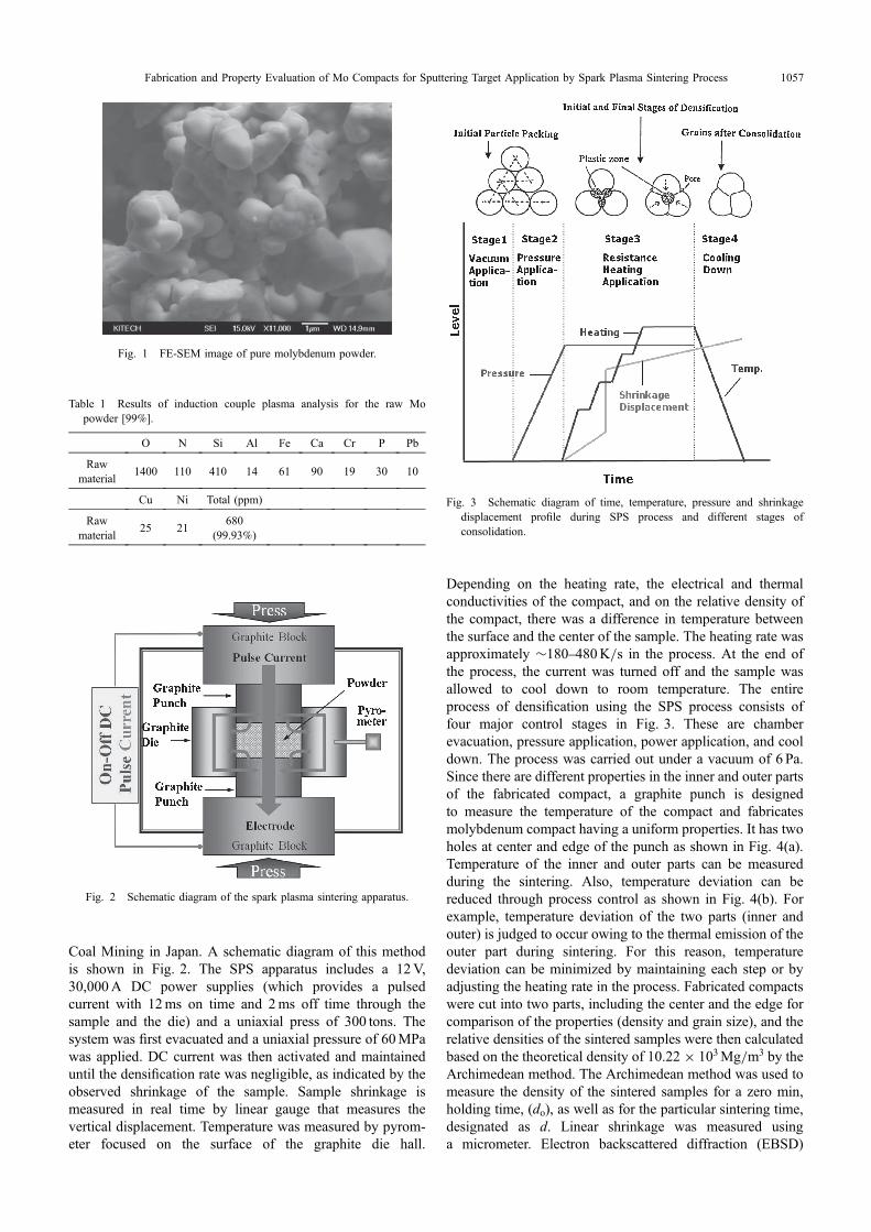
FD ¼ £ þ ðPar=³Þ; ð1Þwhere £ is the interfacial energy, and Pa and r are the appliedpressure and radius of particle, respectively. Figure 7 showsthe density as a function of the sintering temperature ofthe experiments compared with that obtained for the othersintering method.1518) When the compact was sintered byP2C until 1873.15K with 40MPa and 1923.15K with48MPa external pressure, the densities of fabricatedcompacts were 96.0 and 98.5%, respectively.4,7,16) Inaddition, we can compare the densities obtained by SPSwith those of isothermal sintering. The isothermal powdermetallurgical route starts with the hydraulic or isostaticpressing of the molybdenum powder into rods and plates ofvarious geometries and dimensions. The sintering process iscarried out in furnaces at high temperatures (typically in therange of ³2073.152473.15K) and in a hydrogen at-mosphere over long periods of time (³7.210.8 ks) to obtaindensities about 90% of the theoretical density. Figure 7shows the relative densities published in,16,17) which wereestimated after 3.6 ks isothermal sintering. For temperatures
Fig. 6 EBSD images of Mo sputtering targets fabricated by SPS and HIP; (a) SPS (176K/min)-inner, insert inverse pole figure, (b) SPS(176K/min)-outer, (c) HIP-inner, (d) HIP-outer.
Table 2 Grain size and density according to different heating rates (sintered at 2192K under 60MPa pressure).
Compact Size(mm)
Particle size(powder, µm)
Final Sintering Temperature(°)
Pressure(MPa)
Heating rate(°/min)
Final relative density(%)
Grain size(µm)
150 37 2192 60
86Inner 99.7 7.9
Outer 99.2 6.2
140Inner 99.4 4.9
Outer 99.0 4.9
176Inner 99.2 4.4
Outer 99.0 4.1
150 Commercial target (HIP)Inner 99.2 43.8
Outer 99.0 64.4
Fabrication and Property Evaluation of Mo Compacts for Sputtering Target Application by Spark Plasma Sintering Process 1059
higher than 1673.15K, the comparison shows that therelative densities of SPS are comparable with or higher thanthe relative densities generated by isothermal sintering,although the sintering time is very short for SPS. At lowertemperature, isothermal sintered molybdenum bodies becomedenser, which is caused by the higher green density due to ahigher compaction pressure.
The molybdenum compact fabricated by SPS was cut intothe shape of a chip to analyze the purity obtained by the ICPequipment. Since the purity of the compact was measured99.93%, its purity is the same as that of the starting material.This result is shown in Table 3. Moreover the oxygenimpurity of the sputtering target decreased from 1400 to270 ppm, because the cleaning effect is generated by thespark phenomenon between particles during the sintering.
3.2 Evaluation of sputtered molybdenum thin filmsAfter grinding on the surface of the molybdenum target,
SPSed molybdenum target and HIP molybdenum target wereinstalled in the sputtering system. Molybdenum thin filmswere deposited on a glass substrate and used for the backelectrode of the CIGS solar cell. As the detail processcondition, Ar gas was first applied at an initial pressureof 6.5 © 10¹4 Pa (5 © 10¹6 torr). When the thin film wasformed, the pressure was progressed under mixed conditionof high pressure (3.33 Pa) and LP (0.33 Pa) for 3.6 ks at roomtemperature. Specific resistance was calculated througheq. (2) using the face resistance obtained by a 4 point probe.
μ ¼ L � R=A; ð2Þwhere μ is specific resistivity; L is length; and R and A areresistance and sectional area, respectively. The unit of
specific resistance is ®³m at the CIGS unit system, andthere is a countercurrent connection (specific resistance =1/conductivity) with conductivity, demonstrating the abilityof a material to conduct electricity.19) Measured values areshown in Table 4.
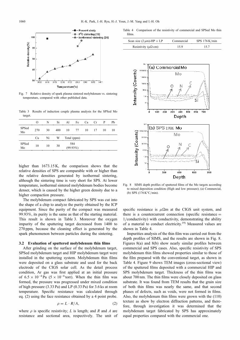
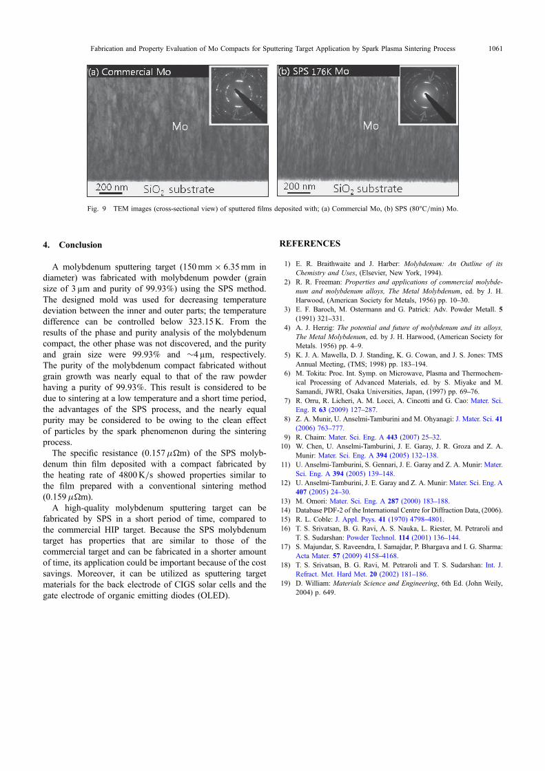
Impurities analysis of the thin film was carried out from thedepth profiles of SIMS, and the results are shown in Fig. 8.Figures 8(a) and 8(b) show nearly similar profiles betweencommercial and SPS cases. Also, specific resistivity of SPSmolybdenum thin films showed properties similar to those ofthe film prepared with the conventional target, as shown inTable 4. Figure 9 shows TEM images (cross-sectional view)of the sputtered films deposited with a commercial HIP andSPS molybdenum target. Thickness of the thin films wasabout 700 nm. The thin films were closely deposited on glasssubstrate. It was found from TEM results that the grain sizeof both thin films was nearly the same, and that secondphases of defects, such as voids, were not formed in films.Also, the molybdenum thin films were grown with the (110)texture as show by electron diffraction patterns, and there-fore, through investigation it was determined that themolybdenum target fabricated by SPS has approximatelyequal properties compared with the commercial one.
Table 3 Results of induction couple plasma analysis for the SPSed Motarget.
O N Si Al Fe Ca Cr P Pb
SPSedMo
270 30 400 10 77 10 17 10 10
Cu Ni W Total (ppm)
SPSedMo
10 10 30584
(99.93%)
Table 4 Comparison of the resistivity of commercial and SPSed Mo thinfilms.
Scan size (2 µm)-HP + LP Commercial SPS 176K/min
Resistivity (µ³·cm) 15.9 15.7
Fig. 8 SIMS depth profiles of sputtered films of the Mo targets accordingto mixed deposition condition (High and low pressure); (a) Commercial,(b) SPS (176K°C/min).
Fig. 7 Relative density of spark plasma sintered molybdenum vs. sinteringtemperature, compared with other published data.
H.-K. Park, J.-H. Ryu, H.-J. Youn, J.-M. Yang and I.-H. Oh1060
4. Conclusion
A molybdenum sputtering target (150mm © 6.35mm indiameter) was fabricated with molybdenum powder (grainsize of 3 µm and purity of 99.93%) using the SPS method.The designed mold was used for decreasing temperaturedeviation between the inner and outer parts; the temperaturedifference can be controlled below 323.15K. From theresults of the phase and purity analysis of the molybdenumcompact, the other phase was not discovered, and the purityand grain size were 99.93% and ³4µm, respectively.The purity of the molybdenum compact fabricated withoutgrain growth was nearly equal to that of the raw powderhaving a purity of 99.93%. This result is considered to bedue to sintering at a low temperature and a short time period,the advantages of the SPS process, and the nearly equalpurity may be considered to be owing to the clean effectof particles by the spark phenomenon during the sinteringprocess.
The specific resistance (0.157®³m) of the SPS molyb-denum thin film deposited with a compact fabricated bythe heating rate of 4800K/s showed properties similar tothe film prepared with a conventional sintering method(0.159®³m).
A high-quality molybdenum sputtering target can befabricated by SPS in a short period of time, compared tothe commercial HIP target. Because the SPS molybdenumtarget has properties that are similar to those of thecommercial target and can be fabricated in a shorter amountof time, its application could be important because of the costsavings. Moreover, it can be utilized as sputtering targetmaterials for the back electrode of CIGS solar cells and thegate electrode of organic emitting diodes (OLED).
REFERENCES
1) E. R. Braithwaite and J. Harber: Molybdenum: An Outline of itsChemistry and Uses, (Elsevier, New York, 1994).
2) R. R. Freeman: Properties and applications of commercial molybde-num and molybdenum alloys, The Metal Molybdenum, ed. by J. H.Harwood, (American Society for Metals, 1956) pp. 1030.
3) E. F. Baroch, M. Ostermann and G. Patrick: Adv. Powder Metall. 5(1991) 321331.
4) A. J. Herzig: The potential and future of molybdenum and its alloys,The Metal Molybdenum, ed. by J. H. Harwood, (American Society forMetals. 1956) pp. 49.
5) K. J. A. Mawella, D. J. Standing, K. G. Cowan, and J. S. Jones: TMSAnnual Meeting, (TMS; 1998) pp. 183194.
6) M. Tokita: Proc. Int. Symp. on Microwave, Plasma and Thermochem-ical Processing of Advanced Materials, ed. by S. Miyake and M.Samandi, JWRI, Osaka Universities, Japan, (1997) pp. 6976.
7) R. Orru, R. Licheri, A. M. Locci, A. Cincotti and G. Cao: Mater. Sci.Eng. R 63 (2009) 127287.
8) Z. A. Munir, U. Anselmi-Tamburini and M. Ohyanagi: J. Mater. Sci. 41(2006) 763777.
9) R. Chaim: Mater. Sci. Eng. A 443 (2007) 2532.10) W. Chen, U. Anselmi-Tamburini, J. E. Garay, J. R. Groza and Z. A.
Munir: Mater. Sci. Eng. A 394 (2005) 132138.11) U. Anselmi-Tamburini, S. Gennari, J. E. Garay and Z. A. Munir: Mater.
Sci. Eng. A 394 (2005) 139148.12) U. Anselmi-Tamburini, J. E. Garay and Z. A. Munir: Mater. Sci. Eng. A
407 (2005) 2430.13) M. Omori: Mater. Sci. Eng. A 287 (2000) 183188.14) Database PDF-2 of the International Centre for Diffraction Data, (2006).15) R. L. Coble: J. Appl. Psys. 41 (1970) 47984801.16) T. S. Srivatsan, B. G. Ravi, A. S. Nauka, L. Riester, M. Petraroli and
T. S. Sudarshan: Powder Technol. 114 (2001) 136144.17) S. Majundar, S. Raveendra, I. Samajdar, P. Bhargava and I. G. Sharma:
Acta Mater. 57 (2009) 41584168.18) T. S. Srivatsan, B. G. Ravi, M. Petraroli and T. S. Sudarshan: Int. J.
Refract. Met. Hard Met. 20 (2002) 181186.19) D. William: Materials Science and Engineering, 6th Ed. (John Weily,
2004) p. 649.
Fig. 9 TEM images (cross-sectional view) of sputtered films deposited with; (a) Commercial Mo, (b) SPS (80°C/min) Mo.
Fabrication and Property Evaluation of Mo Compacts for Sputtering Target Application by Spark Plasma Sintering Process 1061


![Collecting Compact Mirrors & Powder Compacts [DRAFT EXTRACT]](https://static.fdocuments.us/doc/165x107/58edf9c41a28ab245f8b4625/collecting-compact-mirrors-powder-compacts-draft-extract.jpg)


