Extreme ultraviolet lithography : Pushing microchips down to the nanoscale A Wojdyla Center for...
25
Extreme ultraviolet lithography : Pushing microchips down to the nanoscale A Wojdyla Center for X-Ray Optics - LBNL December 12 th , 2013 1
-
Upload
hilda-lang -
Category
Documents
-
view
221 -
download
3
Transcript of Extreme ultraviolet lithography : Pushing microchips down to the nanoscale A Wojdyla Center for...

1
Extreme ultraviolet lithography : Pushing microchips down to the nanoscale
A WojdylaCenter for X-Ray Optics - LBNL
December 12th, 2013
EUV Lithography - All Talk Considered 2
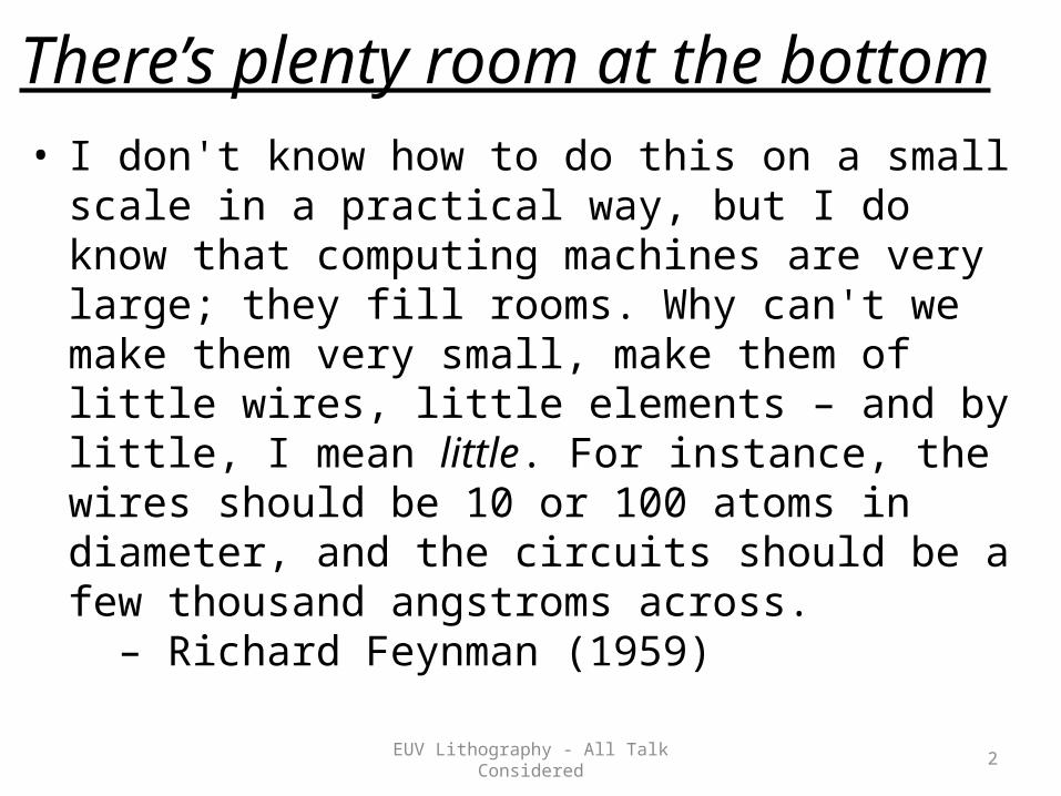
There’s plenty room at the bottom• I don't know how to do this on a small scale in a practical
way, but I do know that computing machines are very large; they fill rooms. Why can't we make them very small, make them of little wires, little elements – and by little, I mean little. For instance, the wires should be 10 or 100 atoms in diameter, and the circuits should be a few thousand angstroms across. – Richard Feynman (1959)
EUV Lithography - All Talk Considered 3
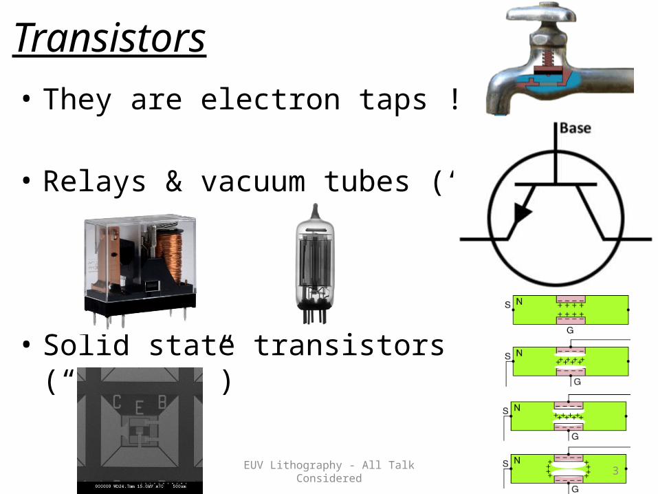
Transistors• They are electron taps !
• Relays & vacuum tubes (“analog”)
• Solid state transistors (“digital”)
EUV Lithography - All Talk Considered 4
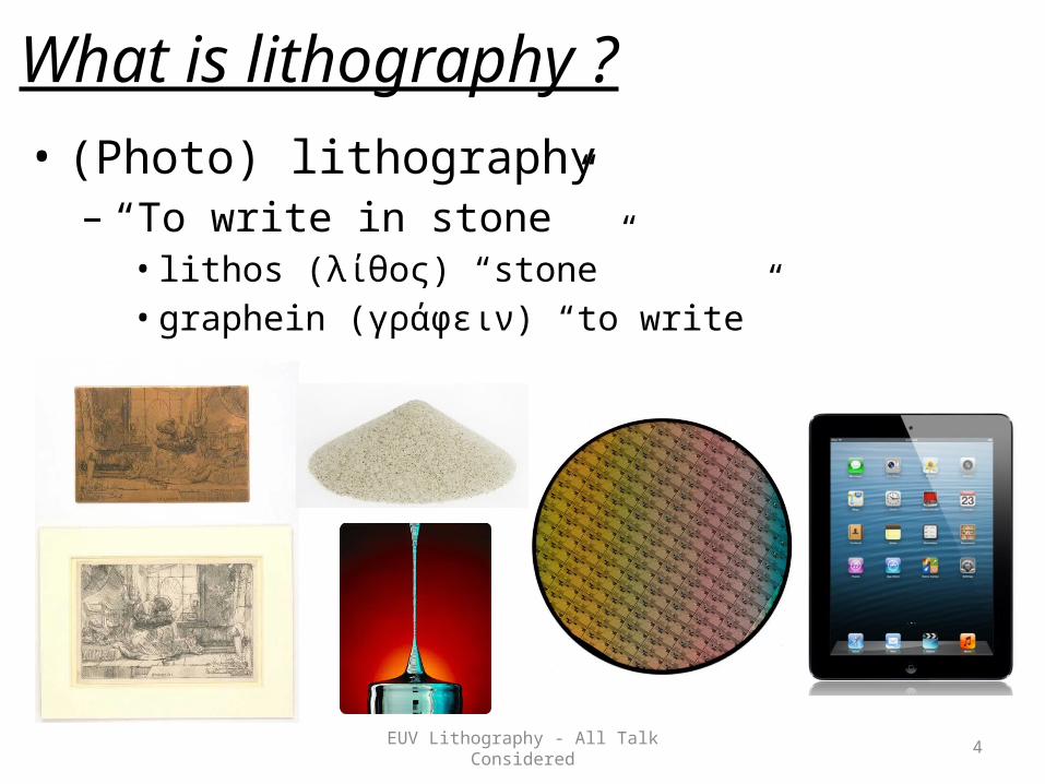
What is lithography ?• (Photo) lithography– “To write in stone”• lithos (λίθος) “stone”• graphein (γράφειν) “to write”

EUV Lithography - All Talk Considered 5
How do you make microchips ? (1/2)
Sour
ce :
Mac
k bo
ok
Inverted microscope
EUV Lithography - All Talk Considered 6
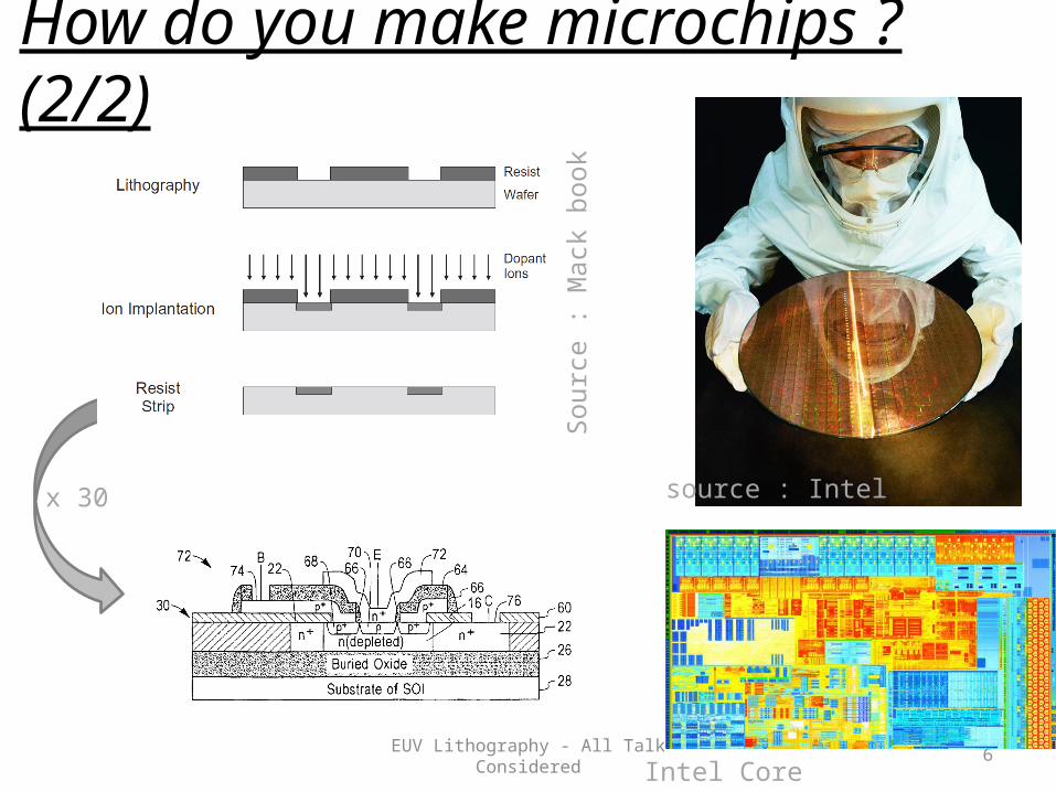
How do you make microchips ? (2/2)
source : Intel
Intel Core
x 30
Sour
ce :
Mac
k bo
ok

EUV Lithography - All Talk Considered 7
How do we make them ?• We don’t actually make microchips,
but we provide the tools to make them
For, in order to work iron, a hammer is needed,and the hammer cannot be forthcoming unless it has been made; but, in order to make it, there was need of another hammer and other tools, and so on to infinity – Spinoza
A crane, as seen from the CXRO coffee room

EUV Lithography - All Talk Considered 8
Source : ASML
Moore’s law“Where a calculator on the ENIAC is equipped with 18,000 vacuum tubes and weighs 30 tons,
computers in the future may have only 1,000 vacuum tubes and perhaps weigh 1.5 tons.” - Popular Mechanics (1949)

EUV Lithography - All Talk Considered 9
Resolution is limited by the wavelength
• Resolution is limited by the wavelength
EUV Lithography - All Talk Considered 10
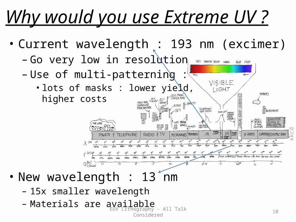
Why would you use Extreme UV ?• Current wavelength : 193 nm (excimer)– Go very low in resolution– Use of multi-patterning : • lots of masks : lower yield,
higher costs
• New wavelength : 13 nm– 15x smaller wavelength– Materials are available
xkcd

EUV Lithography - All Talk Considered 11
Challenges for EUV Lithography• Source– Cyclotrons, FEL, Z-Pinch,
Laser-Produced Plasma– Works in vacuum
• Optics– Only in reflection– Coating (thin film)
• Materials– Appropriate polymers
source : Cymer
source : ALS
EUV Lithography - All Talk Considered 12
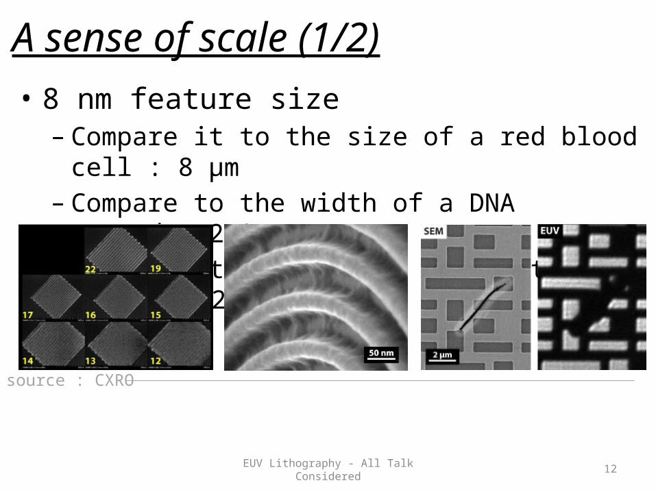
A sense of scale (1/2)• 8 nm feature size– Compare it to the size of a red blood cell : 8 μm– Compare to the width of a DNA strand : 2.3 nm– Compare it to the size of an atom (12C) : 0.2 nm (VdW)
source : CXRO

EUV Lithography - All Talk Considered 1310 μm


EUV Lithography - All Talk Considered 15
A sense of scale (2/2)• 0.1 nm precision (~λ/100)
over the size of a mirror• 1mm precision
over the size of Pacific ocean“Oh man, it’s raining !”
EUV Lithography - All Talk Considered 16
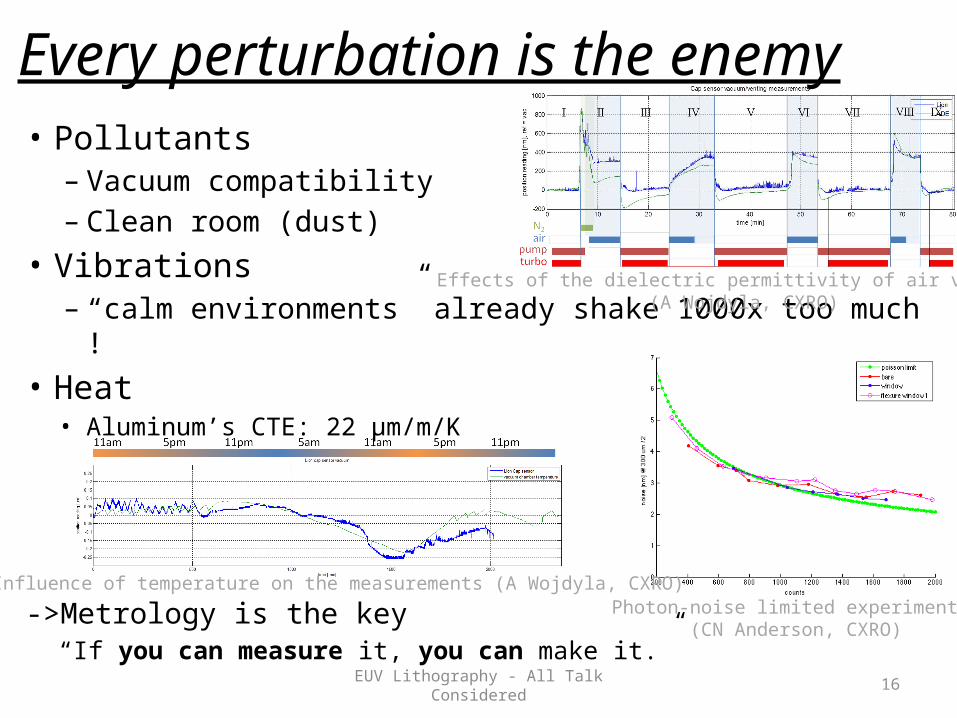
Every perturbation is the enemy• Pollutants– Vacuum compatibility – Clean room (dust)
• Vibrations– “calm environments” already shake 1000x too much !
• Heat• Aluminum’s CTE: 22 μm/m/K
->Metrology is the key“If you can measure it, you can make it.”
Photon-noise limited experiments (CN Anderson, CXRO)
Effects of the dielectric permittivity of air vs. vacuum(A Wojdyla, CXRO)
Influence of temperature on the measurements (A Wojdyla, CXRO)
EUV Lithography - All Talk Considered 17
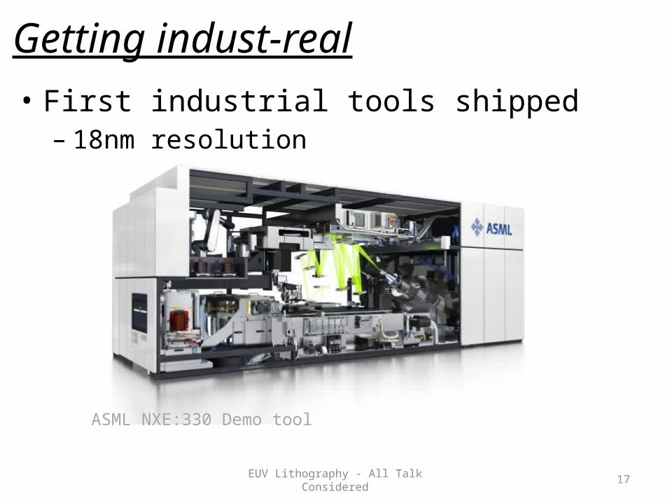
Getting indust-real• First industrial tools shipped– 18nm resolution
ASML NXE:330 Demo tool
EUV Lithography - All Talk Considered 18
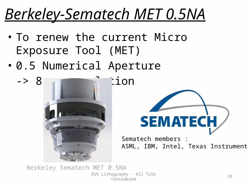
Berkeley-Sematech MET 0.5NA• To renew the current Micro Exposure Tool (MET)• 0.5 Numerical Aperture
-> 8 nm resolution
Sematech members :ASML, IBM, Intel, Texas Instruments,…
Berkeley Sematech MET 0.5NA

EUV Lithography - All Talk Considered 19


21
Designing, simulating, prototyping, tolerancing
wafer leveling systemwavefront sensing optical prototype

EUV Lithography - All Talk Considered 22
Conclusions• Next step in semi-conductor industry
is EUV lithography• It’s not easy, because we have to overcome
Nature’s fundamental limits (so do you!)and environmental factors
• We’ve reached the bottom
• What’s next in tech ?– 3D chips, graphene transistors, spintronics, quantum computers…
xkcd


Drawing from Nobel prizes