Extraction of the sub-bandgap density-of-states in polymer...
6
Extraction of the sub-bandgap density-of-states in polymer thin-film transistors with the multi-frequency capacitance-voltage spectroscopy Jaeman Jang, Jaehyeong Kim, Minkyung Bae, Jaewook Lee, Dong Myong Kim et al. Citation: Appl. Phys. Lett. 100, 133506 (2012); doi: 10.1063/1.3698455 View online: http://dx.doi.org/10.1063/1.3698455 View Table of Contents: http://apl.aip.org/resource/1/APPLAB/v100/i13 Published by the American Institute of Physics. Related Articles Threshold voltage modulation mechanism of AlGaN/GaN metal-insulator-semiconductor high-electron mobility transistors with fluorinated Al2O3 as gate dielectrics Appl. Phys. Lett. 100, 133507 (2012) Positive-negative turbulence-free ghost imaging Appl. Phys. Lett. 100, 131114 (2012) Polarization-induced remote interfacial charge scattering in Al2O3/AlGaN/GaN double heterojunction high electron mobility transistors Appl. Phys. Lett. 100, 132105 (2012) 1-nm-capacitance-equivalent-thickness HfO2/Al2O3/InGaAs metal-oxide-semiconductor structure with low interface trap density and low gate leakage current density Appl. Phys. Lett. 100, 132906 (2012) Second-harmonic generation reveals the oxidation steps in semiconductor processing J. Appl. Phys. 111, 064504 (2012) Additional information on Appl. Phys. Lett. Journal Homepage: http://apl.aip.org/ Journal Information: http://apl.aip.org/about/about_the_journal Top downloads: http://apl.aip.org/features/most_downloaded Information for Authors: http://apl.aip.org/authors Downloaded 30 Mar 2012 to 141.212.212.74. Redistribution subject to AIP license or copyright; see http://apl.aip.org/about/rights_and_permissions
Transcript of Extraction of the sub-bandgap density-of-states in polymer...
Extraction of the sub-bandgap density-of-states in polymer thin-filmtransistors with the multi-frequency capacitance-voltage spectroscopyJaeman Jang, Jaehyeong Kim, Minkyung Bae, Jaewook Lee, Dong Myong Kim et al. Citation: Appl. Phys. Lett. 100, 133506 (2012); doi: 10.1063/1.3698455 View online: http://dx.doi.org/10.1063/1.3698455 View Table of Contents: http://apl.aip.org/resource/1/APPLAB/v100/i13 Published by the American Institute of Physics. Related ArticlesThreshold voltage modulation mechanism of AlGaN/GaN metal-insulator-semiconductor high-electron mobilitytransistors with fluorinated Al2O3 as gate dielectrics Appl. Phys. Lett. 100, 133507 (2012) Positive-negative turbulence-free ghost imaging Appl. Phys. Lett. 100, 131114 (2012) Polarization-induced remote interfacial charge scattering in Al2O3/AlGaN/GaN double heterojunction highelectron mobility transistors Appl. Phys. Lett. 100, 132105 (2012) 1-nm-capacitance-equivalent-thickness HfO2/Al2O3/InGaAs metal-oxide-semiconductor structure with lowinterface trap density and low gate leakage current density Appl. Phys. Lett. 100, 132906 (2012) Second-harmonic generation reveals the oxidation steps in semiconductor processing J. Appl. Phys. 111, 064504 (2012) Additional information on Appl. Phys. Lett.Journal Homepage: http://apl.aip.org/ Journal Information: http://apl.aip.org/about/about_the_journal Top downloads: http://apl.aip.org/features/most_downloaded Information for Authors: http://apl.aip.org/authors
Downloaded 30 Mar 2012 to 141.212.212.74. Redistribution subject to AIP license or copyright; see http://apl.aip.org/about/rights_and_permissions
Extraction of the sub-bandgap density-of-states in polymer thin-filmtransistors with the multi-frequency capacitance-voltage spectroscopy
Jaeman Jang,1 Jaehyeong Kim,1 Minkyung Bae,1 Jaewook Lee,1 Dong Myong Kim,1
Dae Hwan Kim,1,a) Jiyoul Lee,2,a) Bang-Lin Lee,2 Bonwon Koo,2 and Yong Wan Jin2
1School of Electrical Engineering, Kookmin University, Jeongneung-dong, Seongbuk-gu,Seoul 136-702, Korea2Display Device Laboratory, Samsung Advanced Institute of Technology, Yongin-si 446-712, Korea
(Received 22 December 2011; accepted 12 March 2012; published online 30 March 2012)
The multi-frequency capacitance-voltage (C-V) spectroscopy is proposed for extracting the
sub-bandgap density-of-states (DOS) of polymer semiconductors and demonstrated in three
different thiophene-based organic thin-film transistors including poly(3-hexylthiophene),
poly(3,3000-didodecylquaterthiophene), and poly(didodecylquaterthiophene-alt-didodecylbithiazole).
The density of exponential tail and exponential deep states are extracted to be in the range of
3.0� 1018� 1.5� 1019 cm�3 eV�1 and 3.0� 1016� 3.0� 1017 cm�3 eV�1, respectively. The
extracted DOS correspond to the polymer semiconductor-dependence of the measured crystallinity
and mobility. In addition, the extracted DOS values are verified by comparing the measured I-Vcharacteristics with the simulated results through a technology computer-aided design tool. VC 2012American Institute of Physics. [http://dx.doi.org/10.1063/1.3698455]
The sub-bandgap density-of-states (DOS) in organic
films including small-molecule and polymer semiconductors
are closely related to the stability and the device perform-
ance.1 For example, key parameters of the device perform-
ance such as the field-effect mobility, threshold voltage,
subthreshold swing, and electrical stability are considerably
influenced by bulk trap states in the semiconductor or inter-
face states between the semiconductor and the dielectric.
Therefore, it is obvious that the accurate estimation of the
sub-bandgap DOS in the organic semiconductor bulk or at
the interface is of practical importance for the device per-
formance enhancement. More importantly, the performance
of organic semiconductor-based circuits and systems should
be assessed with respect to the DOS-dependence of the small
signal response under a specific bias point because the speed
of circuitry is determined by the small signal response. To
date, various techniques for extracting the DOS in organic
thin-film transistors (TFTs) such as thermally stimulated cur-
rent measurement,2 ultraviolet photoelectron spectroscopy,3
the Meyer-Neldel rule method,4 and the photo-excited
charge collection5 have been demonstrated. However, these
techniques are somewhat destructive schemes and potentially
mutilate the organic semiconductor films, because they are
generally accompanied with the light illumination or thermal
effects.6 More noticeably, the experimental techniques for
directly extracting the DOS in the small signal capacitance
of organic TFTs are rarely reported despite of these
importance.
In this letter, as an efficient technique for extracting the
sub-bandgap DOS of organic semiconductor directly from the
small-signal capacitacne characteristics of organic TFTs, the
multi-frequency cacitance-voltage (C-V) spectroscopy is pro-
posed and demonstrated for extracting the sub-bandgap DOS:
g(E) [cm�3 eV�1], near the valence band maximum (EV) in a
variety of polymer semiconductors including regio-regular
poly(3-hexylthiophene) (P3HT), poly(3,3000-didodecylquater-
thiophene) (PQT-12),7 and poly(didodecylquaterthiophene-
alt-didodecylbithiazole) (PQTBTz-C12).8 As a significant
merit, the multi-frequency C-V sepctroscopy requires no spe-
cial preparation or measurement setup (for the light illumina-
tion and/or thermal effects). The technique directly reflects the
effects of g(E) on the circuit performance because it uses the
gate-to-source/drain (S/D) voltage-dependent small signal
capacitances.
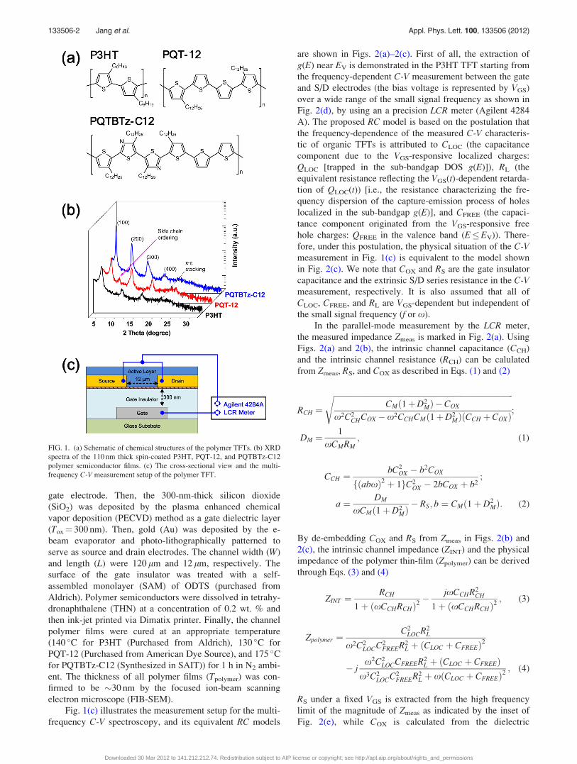
Fig. 1(a) schemetically illustrates chemical structures of
the polymer semiconductors used as active layers (P3HT,
PQT-12, and PQTBTz-C12) of organic TFTs which are well
known materials potentially useful in the printed electronic
applications. In order to investigate the crystalline quality
of the individual polymer semiconductor, we conducted the
x-ray diffraction (XRD) measurement using Cu Ka(k¼ 1.5405 A). Fig. 1(b) displays the XRD spectra of the
polymer semiconductor films obtained by the spin-coating
onto the octadecyltrichlorosilane (ODTS)-treated SiO2 sub-
strates. As shown in these spectra, the PQTBTz-C12 film has
a high intensity with the 4th peak in the (h00) direction,
while the P3HT film and the PQT-12 film have only the 3rd
peak in the same direction. In addition, the d-spacing differ-
ence between PQT-12 (17.0 A) and P3HT (16.5 A) is only
0.5 A even though the alkyl-chain length of PQT-12 is two
times longer than that of P3HT.9 It may lead us to speculate
that the inter-digitation of the alkyl-side chain in the PQT-12
is more efficient than that in the P3HT and the PQT-12 film
has more improved molecular ordering, which should affect
the bulk trap density of the polymer semiconductor in
organic TFTs.
For experimental investigation, we fabricated coplanar
structured TFTs on a glass substrate as shown in Fig. 1(c).
The fabrication process starts with a sputtered deposition of
molybdenum (Mo) as the gate material. The deposited Mo
was patterned by a conventional photo-lithography to form a
a)Authors to whom correspondence should be addressed. Electronic
addresses: [email protected] and [email protected].
0003-6951/2012/100(13)/133506/5/$30.00 VC 2012 American Institute of Physics100, 133506-1
APPLIED PHYSICS LETTERS 100, 133506 (2012)
Downloaded 30 Mar 2012 to 141.212.212.74. Redistribution subject to AIP license or copyright; see http://apl.aip.org/about/rights_and_permissions
gate electrode. Then, the 300-nm-thick silicon dioxide
(SiO2) was deposited by the plasma enhanced chemical
vapor deposition (PECVD) method as a gate dielectric layer
(Tox¼ 300 nm). Then, gold (Au) was deposited by the e-
beam evaporator and photo-lithographically patterned to
serve as source and drain electrodes. The channel width (W)
and length (L) were 120 lm and 12 lm, respectively. The
surface of the gate insulator was treated with a self-
assembled monolayer (SAM) of ODTS (purchased from
Aldrich). Polymer semiconductors were dissolved in tetrahy-
dronaphthalene (THN) at a concentration of 0.2 wt. % and
then ink-jet printed via Dimatix printer. Finally, the channel
polymer films were cured at an appropriate temperature
(140 �C for P3HT (Purchased from Aldrich), 130 �C for
PQT-12 (Purchased from American Dye Source), and 175 �Cfor PQTBTz-C12 (Synthesized in SAIT)) for 1 h in N2 ambi-
ent. The thickness of all polymer films (Tpolymer) was con-
firmed to be �30 nm by the focused ion-beam scanning
electron microscope (FIB-SEM).
Fig. 1(c) illustrates the measurement setup for the multi-
frequency C-V spectroscopy, and its equivalent RC models
are shown in Figs. 2(a)–2(c). First of all, the extraction of
g(E) near EV is demonstrated in the P3HT TFT starting from
the frequency-dependent C-V measurement between the gate
and S/D electrodes (the bias voltage is represented by VGS)
over a wide range of the small signal frequency as shown in
Fig. 2(d), by using an a precision LCR meter (Agilent 4284
A). The proposed RC model is based on the postulation that
the frequency-dependence of the measured C-V characteris-
tic of organic TFTs is attributed to CLOC (the capacitance
component due to the VGS-responsive localized charges:
QLOC [trapped in the sub-bandgap DOS g(E)]), RL (the
equivalent resistance reflecting the VGS(t)-dependent retarda-
tion of QLOC(t)) [i.e., the resistance characterizing the fre-
quency dispersion of the capture-emission process of holes
localized in the sub-bandgap g(E)], and CFREE (the capaci-
tance component originated from the VGS-responsive free
hole charges: QFREE in the valence band (E�EV)). There-
fore, under this postulation, the physical situation of the C-Vmeasurement in Fig. 1(c) is equivalent to the model shown
in Fig. 2(c). We note that COX and RS are the gate insulator
capacitance and the extrinsic S/D series resistance in the C-Vmeasurement, respectively. It is also assumed that all of
CLOC, CFREE, and RL are VGS-dependent but independent of
the small signal frequency (f or x).
In the parallel-mode measurement by the LCR meter,
the measured impedance Zmeas is marked in Fig. 2(a). Using
Figs. 2(a) and 2(b), the intrinsic channel capacitance (CCH)
and the intrinsic channel resistance (RCH) can be calulated
from Zmeas, RS, and COX as described in Eqs. (1) and (2)
RCH ¼ffiffiffiffiffiffiffiffiffiffiffiffiffiffiffiffiffiffiffiffiffiffiffiffiffiffiffiffiffiffiffiffiffiffiffiffiffiffiffiffiffiffiffiffiffiffiffiffiffiffiffiffiffiffiffiffiffiffiffiffiffiffiffiffiffiffiffiffiffiffiffiffiffiffiffiffiffiffiffiffiffiffiffiffiffiffiffiffiffiffiffi
CMð1þD2MÞ �COX
x2C2CHCOX �x2CCHCMð1þD2
MÞðCCH þCOXÞ
s;
DM ¼1
xCMRM; (1)
CCH ¼bC2
OX � b2COX
fðabxÞ2 þ 1gC2OX � 2bCOX þ b2
;
a ¼ DM
xCMð1þ D2MÞ� RS; b ¼ CMð1þ D2
MÞ: (2)
By de-embedding COX and RS from Zmeas in Figs. 2(b) and
2(c), the intrinsic channel impedance (ZINT) and the physical
impedance of the polymer thin-film (Zpolymer) can be derived
through Eqs. (3) and (4)
ZINT ¼RCH
1þ ðxCCHRCHÞ2� jxCCHR2
CH
1þ ðxCCHRCHÞ2; (3)
Zpolymer ¼C2
LOCR2L
x2C2LOCC2
FREER2L þ ðCLOC þ CFREEÞ2
� jx2C2
LOCCFREER2L þ ðCLOC þ CFREEÞ
x3C2LOCC2
FREER2L þ xðCLOC þ CFREEÞ2
; (4)
RS under a fixed VGS is extracted from the high frequency
limit of the magnitude of Zmeas as indicated by the inset of
Fig. 2(e), while COX is calculated from the dielectric
FIG. 1. (a) Schematic of chemical structures of the polymer TFTs. (b) XRD
spectra of the 110 nm thick spin-coated P3HT, PQT-12, and PQTBTz-C12
polymer semiconductor films. (c) The cross-sectional view and the multi-
frequency C-V measurement setup of the polymer TFT.
133506-2 Jang et al. Appl. Phys. Lett. 100, 133506 (2012)
Downloaded 30 Mar 2012 to 141.212.212.74. Redistribution subject to AIP license or copyright; see http://apl.aip.org/about/rights_and_permissions
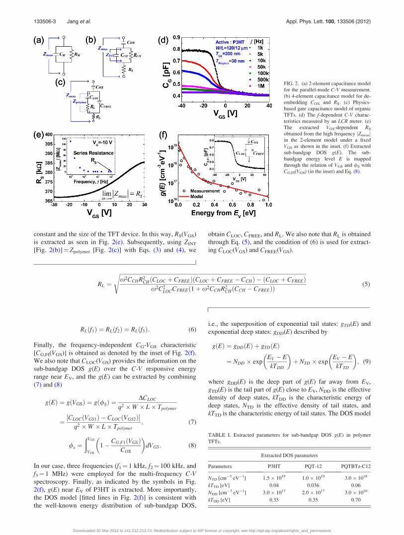
constant and the size of the TFT device. In this way, RS(VGS)
is extracted as seen in Fig. 2(e). Subsequently, using ZINT
[Fig. 2(b)]¼ Zpolymer [Fig. 2(c)] with Eqs. (3) and (4), we
obtain CLOC, CFREE, and RL. We also note that RL is obtained
through Eq. (5), and the condition of (6) is used for extract-
ing CLOC(VGS) and CFREE(VGS).
RL ¼ffiffiffiffiffiffiffiffiffiffiffiffiffiffiffiffiffiffiffiffiffiffiffiffiffiffiffiffiffiffiffiffiffiffiffiffiffiffiffiffiffiffiffiffiffiffiffiffiffiffiffiffiffiffiffiffiffiffiffiffiffiffiffiffiffiffiffiffiffiffiffiffiffiffiffiffiffiffiffiffiffiffiffiffiffiffiffiffiffiffiffiffiffiffiffiffiffiffiffiffiffiffiffiffiffiffiffiffiffiffiffiffiffiffiffiffiffiffiffiffiffiffiffiffiffiffiffiffiffiffiffiffiffiffiffix2CCHR2
CHðCLOC þ CFREEÞðCLOC þ CFREE � CCHÞ � ðCLOC þ CFREEÞx2C2
LOCCFREEð1þ x2CCHR2CHðCCH � CFREEÞÞ
s(5)
RLðf1Þ ¼ RLðf2Þ ¼ RLðf3Þ: (6)
Finally, the frequency-independent CG-VGS characteristic
[CG,FI(VGS)] is obtained as denoted by the inset of Fig. 2(f).
We also note that CLOC(VGS) provides the information on the
sub-bandgap DOS g(E) over the C-V responsive energy
range near EV, and the g(E) can be extracted by combining
(7) and (8)
gðEÞ ¼ gðVGSÞ ¼ gð/SÞ ¼DCLOC
q2 �W � L� Tpolymer
¼ ½CLOCðVGS1Þ � CLOCðVGS2Þ�q2 �W � L� Tpolymer
; (7)
/s ¼ðVGS
VFB
1� CG;F1ðVGSÞCOX
� �dVGS: (8)
In our case, three frequencies (f1¼ 1 kHz, f2¼ 100 kHz, and
f3¼ 1 MHz) were employed for the multi-frequency C-Vspectroscopy. Finally, as indicated by the symbols in Fig.
2(f), g(E) near EV of P3HT is extracted. More importantly,
the DOS model [fitted lines in Fig. 2(f)] is consistent with
the well-known energy distribution of sub-bandgap DOS,
i.e., the superposition of exponential tail states: gTD(E) and
exponential deep states: gDD(E) described by
gðEÞ ¼ gDDðEÞ þ gTDðEÞ
¼ NDD � expEV � E
kTDD
� �þ NTD � exp
EV � E
kTTD
� �; (9)
where gDD(E) is the deep part of g(E) far away from EV,
gTD(E) is the tail part of g(E) close to EV, NDD is the effective
density of deep states, kTDD is the characteristic energy of
deep states, NTD is the effective density of tail states, and
kTTD is the characteristic energy of tail states. The DOS model
TABLE I. Extracted parameters for sub-bandgap DOS g(E) in polymer
TFTs.
Extracted DOS parameters
Parameters P3HT PQT-12 PQTBTz-C12
NTD [cm�3 eV�1] 1.5 � 1019 1.0 � 1019 3.0 � 1018
kTTD [eV] 0.04 0.036 0.06
NDD [cm�3 eV�1] 3.0 � 1017 2.0 � 1017 3.0 � 1016
kTDD [eV] 0.35 0.35 0.70
FIG. 2. (a) 2-element capacitance model
for the parallel-mode C-V measurement.
(b) 4-element capacitance model for de-
embedding COX and RS. (c) Physics-
based gate capacitance model of organic
TFTs. (d) The f-dependent C-V charac-
teristics measured by an LCR meter. (e)
The extracted VGS-dependent RS
obtained from the high frequency jZmeasjin the 2-element model under a fixed
VGS as shown in the inset. (f) Extracted
sub-bandgap DOS g(E). The sub-
bandgap energy level E is mapped
through the relation of VGS and /S with
CG,FI(VGS) (in the inset) and Eq. (8).
133506-3 Jang et al. Appl. Phys. Lett. 100, 133506 (2012)
Downloaded 30 Mar 2012 to 141.212.212.74. Redistribution subject to AIP license or copyright; see http://apl.aip.org/about/rights_and_permissions
parameters (NTD¼ 1.5� 1019 cm�3�eV�1, NDD¼ 3.0� 1017
cm�3�eV�1, kTTD¼ 0.04 eV, and kTDD¼ 0.35 eV) are also
summarized in Table I.
Conclusively, for the P3HT-based TFTs, we can sum-
marize all procedure of extracting g(E) as follows. The
frequency-sensitive nature of the measured CG-VGS charac-
teristics in Fig. 2(d) can be modeled as the frequency disper-
sion of the RC network in Fig. 2(c), which consists of the
frequency-independent RC components such as COX, CLOC,
CFREE, RL, and RS. Then, we obtain CLOC(VGS) and translate
it into g(E) [as indicated in Eq. (7)] through a mapping to the
sub-bandgap energy level via CG,FI(VGS) and Eq. (8). A
detailed procedure of extracting g(E) from the multi-
frequency C-V spectroscopy was described in the example of
inorganic counterpart.10 We note that the proposed approach
provides a complicated nonlinear relationship between the
surface potential (/S) and VGS in a simple manner, with the
aid of CG,FI(VGS) and Eq. (8). It means that the energy distri-
bution of the extracted g(E) is exactly matched with the sub-
bandgap energy level of the polymer thin-films.
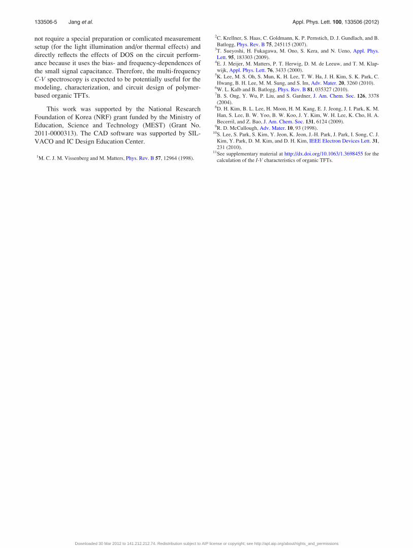
In order to verify the universality of the proposed
approach, g(E) is also extracted from PQT-12 and PQTBTz-
C12 TFTs by the same procedure and model. In Fig. 3, we
overlaid the g(E) profiles of P3HT, PQT-12, and PQTBTz-
C12 TFTs, which are obtained from the multi-frequency C-Vspectroscopy of 3 polymer semiconductor TFTs. DOS pa-
rameters are also summarized in Table I. It should be noted
that the polymer semicondutor with the superior crystallinity
in Fig. 1(b) [PQTBTZ-C12] clearly shows the lowest value
of g(E) and vice versa. From this result, we expect that the
mobility of PQTBTz-C12 TFT is higher than those of two
other TFTs. This is because with increased g(E), i.e., NTD,
more holes should be spent for the Fermi-enery level to
approach closer to EV, which is followed by the mobility
degradation under a fixed bias.
In order to quantitatively verify the extracted DOS, the
DOS model in Table I is incorporated into the TCAD (tech-
nology computer-aided design) simulation, and the results
(line) are compared with the measured transfer characteris-
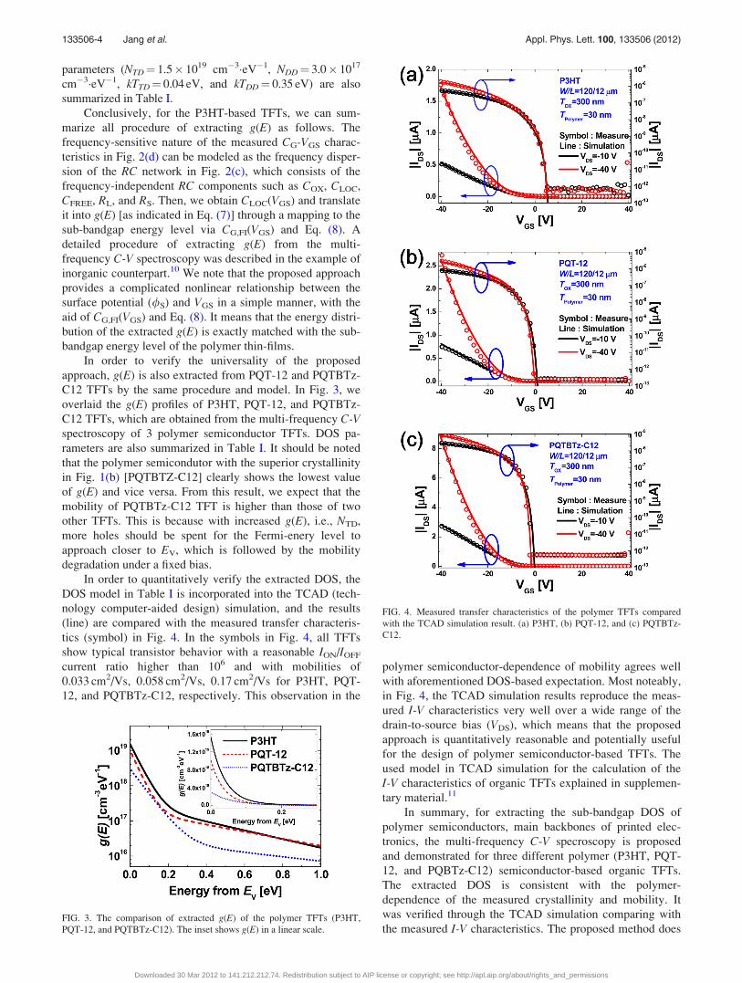
tics (symbol) in Fig. 4. In the symbols in Fig. 4, all TFTs
show typical transistor behavior with a reasonable ION/IOFF
current ratio higher than 106 and with mobilities of
0.033 cm2/Vs, 0.058 cm2/Vs, 0.17 cm2/Vs for P3HT, PQT-
12, and PQTBTz-C12, respectively. This observation in the
polymer semiconductor-dependence of mobility agrees well
with aforementioned DOS-based expectation. Most noteably,
in Fig. 4, the TCAD simulation results reproduce the meas-
ured I-V characteristics very well over a wide range of the
drain-to-source bias (VDS), which means that the proposed
approach is quantitatively reasonable and potentially useful
for the design of polymer semiconductor-based TFTs. The
used model in TCAD simulation for the calculation of the
I-V characteristics of organic TFTs explained in supplemen-
tary material.11
In summary, for extracting the sub-bandgap DOS of
polymer semiconductors, main backbones of printed elec-
tronics, the multi-frequency C-V specroscopy is proposed
and demonstrated for three different polymer (P3HT, PQT-
12, and PQBTz-C12) semiconductor-based organic TFTs.
The extracted DOS is consistent with the polymer-
dependence of the measured crystallinity and mobility. It
was verified through the TCAD simulation comparing with
the measured I-V characteristics. The proposed method doesFIG. 3. The comparison of extracted g(E) of the polymer TFTs (P3HT,
PQT-12, and PQTBTz-C12). The inset shows g(E) in a linear scale.
FIG. 4. Measured transfer characteristics of the polymer TFTs compared
with the TCAD simulation result. (a) P3HT, (b) PQT-12, and (c) PQTBTz-
C12.
133506-4 Jang et al. Appl. Phys. Lett. 100, 133506 (2012)
Downloaded 30 Mar 2012 to 141.212.212.74. Redistribution subject to AIP license or copyright; see http://apl.aip.org/about/rights_and_permissions
not require a special preparation or comlicated measurement
setup (for the light illumination and/or thermal effects) and
directly reflects the effects of DOS on the circuit perform-
ance because it uses the bias- and frequency-dependences of
the small signal capacitance. Therefore, the multi-frequency
C-V spectroscopy is expected to be potentially useful for the
modeling, characterization, and circuit design of polymer-
based organic TFTs.
This work was supported by the National Research
Foundation of Korea (NRF) grant funded by the Ministry of
Education, Science and Technology (MEST) (Grant No.
2011-0000313). The CAD software was supported by SIL-
VACO and IC Design Education Center.
1M. C. J. M. Vissenberg and M. Matters, Phys. Rev. B 57, 12964 (1998).
2C. Krellner, S. Haas, C. Goldmann, K. P. Pernstich, D. J. Gundlach, and B.
Batlogg, Phys. Rev. B 75, 245115 (2007).3T. Sueyoshi, H. Fukagawa, M. Ono, S. Kera, and N. Ueno, Appl. Phys.
Lett. 95, 183303 (2009).4E. J. Meijer, M. Matters, P. T. Herwig, D. M. de Leeuw, and T. M. Klap-
wijk, Appl. Phys. Lett. 76, 3433 (2000).5K. Lee, M. S. Oh, S. Mun, K. H. Lee, T. W. Ha, J. H. Kim, S. K. Park, C.
Hwang, B. H. Lee, M. M. Sung, and S. Im, Adv. Mater. 20, 3260 (2010).6W. L. Kalb and B. Batlogg, Phys. Rev. B 81, 035327 (2010).7B. S. Ong, Y. Wu, P. Liu, and S. Gardner, J. Am. Chem. Soc. 126, 3378
(2004).8D. H. Kim, B. L. Lee, H. Moon, H. M. Kang, E. J. Jeong, J. I. Park, K. M.
Han, S. Lee, B. W. Yoo, B. W. Koo, J. Y. Kim, W. H. Lee, K. Cho, H. A.
Becerril, and Z. Bao, J. Am. Chem. Soc. 131, 6124 (2009).9R. D. McCullough, Adv. Mater. 10, 93 (1998).
10S. Lee, S. Park, S. Kim, Y. Jeon, K. Jeon, J.-H. Park, J. Park, I. Song, C. J.
Kim, Y. Park, D. M. Kim, and D. H. Kim, IEEE Electron Devices Lett. 31,
231 (2010).11See supplementary material at http://dx.doi.org/10.1063/1.3698455 for the
calculation of the I-V characteristics of organic TFTs.
133506-5 Jang et al. Appl. Phys. Lett. 100, 133506 (2012)
Downloaded 30 Mar 2012 to 141.212.212.74. Redistribution subject to AIP license or copyright; see http://apl.aip.org/about/rights_and_permissions