Exploring Carbon Nanotube Bundle Global …sudeep/wp-content/uploads/c23.pdfExploring Carbon...
6
Exploring Carbon Nanotube Bundle Global Interconnects for Chip Multiprocessor Applications Sudeep Pasricha * , Nikil Dutt † , Fadi J. Kurdahi † , * Colorado State University, Fort Collins, CO † University of California, Irvine, CA [email protected] {dutt, kurdahi}@uci.edu Abstract The current paradigm of using Cu interconnects for on-chip global communication is rapidly becoming a serious performance bottleneck in ultra-deep submicron (UDSM) technologies. Carbon nanotube (CNT) based interconnects have been proposed as an alternative, because of their remarkable conductive, mechanical and thermal properties. In this paper, we investigate the system level performance of single-walled CNT (SWCNT) bundles, and mixed SWCNT/multi-walled CNT (MWCNT) bundles. Detailed RLC equivalent circuit models for conventional Cu and CNT bundle interconnects are described and used to determine propagation delays. These models are then incorporated into a system-level environment to estimate the impact of using CNT bundle global interconnects on the overall performance of several multi-core chip multiprocessor (CMP) applications. Our results indicate that the CNT bundle alternatives have a slight performance advantage over Cu global interconnects. With further improvements in CNT fabrication technology, we show how CNT bundle-based interconnects can significantly outperform Cu interconnects. 1. Introduction As technology scales into the ultra-deep submicron (UDSM) region, interconnect design is becoming a major roadblock in realizing emerging multi-core chip multiprocessors (CMPs) that have tens to hundreds of components integrated on a single chip [1]. Interconnects used in CMPs can be classified into two categories: local interconnects, that are used for short distance communication, and have a delay of less than a clock cycle, and global interconnects, that are used for long distance communication to distribute data, clock, power supply and ground across the chip, and have a delay spanning multiple clock cycles [23]. According to the International Roadmap for Semiconductors (ITRS) 2005 [4], global interconnect performance has become one of the semiconductor industry’s topmost challenges. Conventional copper (Cu) global interconnects have become increasingly susceptible to electromigration at high current densities (>10 6 A/cm 2 ) leading to considerable degradation in reliability [2]. Additionally, as interconnect dimensions are scaled down, rising crosstalk coupling noise and parasitic resistivity due to electron-surface and grain-boundary scatterings cause global interconnect delay to increase rapidly [3]. There is therefore a critical need to investigate innovative global interconnect alternatives to Cu. Recently, there has been tremendous interest in carbon nanotubes (CNTs) as a possible replacement for Cu interconnects in future technologies [5]-[8]. Depending on the direction in which they are rolled (called chirality) CNTs can behave either as semiconductors or conductors. Conducting (or metallic) CNTs possess many extraordinary properties that make them promising candidates for implementing interconnects in UDSM technologies. Due to their covalently bonded structure, they are highly resistant to electromigration and other sources of physical breakdown [5]. They can support very high current densities with very little performance degradation. For instance, it was shown in [15] that the current carrying capacity of CNTs did not degrade even after 350 hours at current densities of ~10 10 A/cm 2 at 250 ºC. CNTs possess high thermal conductivity in the range of 1700–3000 W/m·K [16]. They also have much better conductivity properties than Cu owing to longer electron mean free path (MFP) lengths in the micrometer range, compared to nanometer range MFP lengths for Cu [7]. CNTs can be broadly classified into single-walled carbon nanotubes (SWCNTs) [9]-[11] and multi-walled carbon nanotubes (MWCNTs) [12]-[13]. SWCNTs consist of a single sheet of graphene rolled into a cylindrical tube, with a diameter in the nanometer range. MWCNTs consist of two or more SWCNTs concentrically wrapped around each other, with diameters ranging from a few to several hundred nanometers. For on-chip global interconnects, bundles of SWCNTs and mixed SWCNT/MWCNTs (Fig. 1) are of special interest because of their superior conductivity properties. An SWCNT bundle consists of several SWCNTs packed together in parallel [12], whereas a mixed SWCNT/ MWCNT bundle consists of a combination of SWCNTs and MWCNTs packed together in parallel [13]. Fig. 1. Carbon nanotube (CNT) bundle interconnect alternatives: SWCNT bundle and mixed SWCNT/MWCNT bundle The question arises: how do CNT bundles compare against Cu as global interconnect materials? While there has been a lot of interest in CNT-based interconnects in recent years, there are unfortunately few studies that compare CNT bundle interconnects with Cu interconnects at the system level. As complex chip multiprocessor (CMP) systems become the norm, it is critical to evaluate the impact of using promising new interconnect paradigms such as CNT bundles in such systems. Such an analysis allows designers to understand potential benefits and limitations of CNT bundle technology. It also gives them a true insight into realistic gains that can be achieved by switching to CNT bundle-based global interconnects in the future. In this paper, we present such a comparative performance analysis of conventional Cu global interconnects with the CNT bundle global interconnect alternatives shown in Fig. 1. We investigate the performance impact of using CNT bundle global interconnects in place of conventional Cu global interconnects at the system-level for several CMP applications. Detailed RLC equivalent circuit models for Cu and CNT bundle interconnects are described and used to determine propagation delays. The CNT equivalent RLC circuit models capture the statistical distribution of metallic nanotubes while accurately incorporating recent experimental and theoretical results on inductance, crosstalk capacitance and ohmic resistance. These models are then incorporated into a system level environment to metallic semiconducting SWCNT Bundle Mixed Bundle SWCNT MWCNT 2009 22nd International Conference on VLSI Design 1063-9667/09 $25.00 © 2009 IEEE DOI 10.1109/VLSI.Design.2009.84 499 Authorized licensed use limited to: COLORADO STATE UNIVERSITY. Downloaded on August 22, 2009 at 14:22 from IEEE Xplore. Restrictions apply.
Transcript of Exploring Carbon Nanotube Bundle Global …sudeep/wp-content/uploads/c23.pdfExploring Carbon...

Exploring Carbon Nanotube Bundle Global Interconnects for Chip Multiprocessor Applications
Sudeep Pasricha*, Nikil Dutt†, Fadi J. Kurdahi†,
*Colorado State University, Fort Collins, CO †University of California, Irvine, CA [email protected] dutt, [email protected]
Abstract
The current paradigm of using Cu interconnects for on-chip global communication is rapidly becoming a serious performance bottleneck in ultra-deep submicron (UDSM) technologies. Carbon nanotube (CNT) based interconnects have been proposed as an alternative, because of their remarkable conductive, mechanical and thermal properties. In this paper, we investigate the system level performance of single-walled CNT (SWCNT) bundles, and mixed SWCNT/multi-walled CNT (MWCNT) bundles. Detailed RLC equivalent circuit models for conventional Cu and CNT bundle interconnects are described and used to determine propagation delays. These models are then incorporated into a system-level environment to estimate the impact of using CNT bundle global interconnects on the overall performance of several multi-core chip multiprocessor (CMP) applications. Our results indicate that the CNT bundle alternatives have a slight performance advantage over Cu global interconnects. With further improvements in CNT fabrication technology, we show how CNT bundle-based interconnects can significantly outperform Cu interconnects.
1. Introduction As technology scales into the ultra-deep submicron (UDSM)
region, interconnect design is becoming a major roadblock in realizing emerging multi-core chip multiprocessors (CMPs) that have tens to hundreds of components integrated on a single chip [1]. Interconnects used in CMPs can be classified into two categories: local interconnects, that are used for short distance communication, and have a delay of less than a clock cycle, and global interconnects, that are used for long distance communication to distribute data, clock, power supply and ground across the chip, and have a delay spanning multiple clock cycles [23]. According to the International Roadmap for Semiconductors (ITRS) 2005 [4], global interconnect performance has become one of the semiconductor industry’s topmost challenges. Conventional copper (Cu) global interconnects have become increasingly susceptible to electromigration at high current densities (>106 A/cm2) leading to considerable degradation in reliability [2]. Additionally, as interconnect dimensions are scaled down, rising crosstalk coupling noise and parasitic resistivity due to electron-surface and grain-boundary scatterings cause global interconnect delay to increase rapidly [3]. There is therefore a critical need to investigate innovative global interconnect alternatives to Cu.
Recently, there has been tremendous interest in carbon nanotubes (CNTs) as a possible replacement for Cu interconnects in future technologies [5]-[8]. Depending on the direction in which they are rolled (called chirality) CNTs can behave either as semiconductors or conductors. Conducting (or metallic) CNTs possess many extraordinary properties that make them promising candidates for implementing interconnects in UDSM technologies. Due to their covalently bonded structure, they are highly resistant to electromigration and other sources of physical breakdown [5]. They can support very high current densities with very little performance degradation. For instance, it was shown in [15] that the current carrying capacity of CNTs did not degrade even after 350 hours at current densities of ~1010 A/cm2 at 250 ºC. CNTs possess high
thermal conductivity in the range of 1700–3000 W/m·K [16]. They also have much better conductivity properties than Cu owing to longer electron mean free path (MFP) lengths in the micrometer range, compared to nanometer range MFP lengths for Cu [7].
CNTs can be broadly classified into single-walled carbon nanotubes (SWCNTs) [9]-[11] and multi-walled carbon nanotubes (MWCNTs) [12]-[13]. SWCNTs consist of a single sheet of graphene rolled into a cylindrical tube, with a diameter in the nanometer range. MWCNTs consist of two or more SWCNTs concentrically wrapped around each other, with diameters ranging from a few to several hundred nanometers. For on-chip global interconnects, bundles of SWCNTs and mixed SWCNT/MWCNTs (Fig. 1) are of special interest because of their superior conductivity properties. An SWCNT bundle consists of several SWCNTs packed together in parallel [12], whereas a mixed SWCNT/ MWCNT bundle consists of a combination of SWCNTs and MWCNTs packed together in parallel [13].
Fig. 1. Carbon nanotube (CNT) bundle interconnect alternatives: SWCNT bundle and mixed SWCNT/MWCNT bundle
The question arises: how do CNT bundles compare against Cu as
global interconnect materials? While there has been a lot of interest in CNT-based interconnects in recent years, there are unfortunately few studies that compare CNT bundle interconnects with Cu interconnects at the system level. As complex chip multiprocessor (CMP) systems become the norm, it is critical to evaluate the impact of using promising new interconnect paradigms such as CNT bundles in such systems. Such an analysis allows designers to understand potential benefits and limitations of CNT bundle technology. It also gives them a true insight into realistic gains that can be achieved by switching to CNT bundle-based global interconnects in the future.
In this paper, we present such a comparative performance analysis of conventional Cu global interconnects with the CNT bundle global interconnect alternatives shown in Fig. 1. We investigate the performance impact of using CNT bundle global interconnects in place of conventional Cu global interconnects at the system-level for several CMP applications. Detailed RLC equivalent circuit models for Cu and CNT bundle interconnects are described and used to determine propagation delays. The CNT equivalent RLC circuit models capture the statistical distribution of metallic nanotubes while accurately incorporating recent experimental and theoretical results on inductance, crosstalk capacitance and ohmic resistance. These models are then incorporated into a system level environment to
metallic
semiconducting
SWCNT Bundle
Mixed Bundle
SWCNT
MWCNT
2009 22nd International Conference on VLSI Design
1063-9667/09 $25.00 © 2009 IEEE
DOI 10.1109/VLSI.Design.2009.84
499
Authorized licensed use limited to: COLORADO STATE UNIVERSITY. Downloaded on August 22, 2009 at 14:22 from IEEE Xplore. Restrictions apply.

estimate the impact of using CNT bundle-based global interconnects on the overall performance of several heterogeneous CMP applications with diverse data traffic profiles. Our results indicate that CNT bundle alternatives have a slight performance advantage over Cu global interconnects, providing up to a 1.5× speedup for the applications explored. With further improvements in CNT fabrication technology, we show how CNT bundle interconnects can significantly outperform Cu interconnects.
2. Related Work
In the last few years, there has been a lot of interest in studying the properties carbon nanotubes (CNTs). Researchers have developed RLC circuit models for CNT interconnect alternatives and compared their performance with Cu interconnects at the circuit level. RLC circuit models have been developed for isolated SWCNTs [9]-[11], SWCNT bundles [8][12][14] and MWCNTs [12]-[13]. Recently, conductance and inductance models for mixed SWCNT/MWCNT bundles were also introduced [13][40]. Other studies have presented some interesting discussions on the impact of process variations on CNT performance [18] and the possibility of CNTs replacing Cu interconnects in future FPGA fabrics [19]. However, none of these studies have analyzed the impact of using CNT interconnects instead of Cu interconnects at the system-level. Recently, [17] explored the possibility of using CNTs as global interconnect buses. The authors described a dual-walled CNT global bus and presented experiments to show that it outperforms SWCNT global buses. In this work, we explore the possibility of using CNT bundles as global interconnects. Unlike [17], we present comparisons with conventional Cu global interconnects, and investigate CNT bundle performance for several heterogeneous CMP applications.
3. SWCNT and MWCNT Circuit Models
In this section, we present an overview of SWCNT and MWCNT equivalent RLC interconnect circuit models derived from literature. These models are used as the foundation for the circuit models of the CNT bundle interconnects, described in Section 4.
3.1 SWCNT The fundamental (quantum) resistance of an SWCNT can be
determined using the Landauer-Buttker formula [5], RQ=h/4e2 and is about 6.45kΩ. This is the constant resistance of an SWCNT of length less than or equal to its mean free path length λ. For longer lengths, SWCNT resistance has been shown to depend on its length and bias voltage [11]. For bias voltage less than the critical bias (< 0.16V for global wires [22]), the SWCNT resistance is:
4
,
4
, 1
where h is Planck’s constant, e is the charge of an electron, l is the SWCNT length and λ is the mean free path (MFP) length. Ideally, the mean free path (λ) value is in the order of several µm. However, a rigorous analysis has shown that practically, λ is around 1 µm [10].
For SWCNT interconnects, three types of capacitance should be considered: an electrostatic capacitance with the ground (CEG), a coupling capacitance with any adjacent SWCNTs (CEC), and an intrinsic quantum capacitance (CQ) [6]. The electrostatic capacitance per unit length between an SWCNT and the ground plane is:
2
2 2
where ε is the permittivity of the dielectric and H is the distance between the SWCNT and ground plane. Similarly, the electrostatic capacitance per unit length between two parallel SWCNTs is:
3
where s is the inter-SWCNT spacing and dt is the SWCNT diameter. Finally, the SWCNT quantum capacitance per unit length is:
2
4
SWCNTs have been shown to consist of four co-propagating quantum channels, and therefore the effective SWCNT quantum capacitance is 4CQ [6]. As per the analysis in [24], 4CQ is in series with a parallel combination of CEG and CEC. Because electrostatic coupling between non-adjacent SWCNTs is very weak compared to coupling between adjacent SWCNTs, the coupling capacitance between nonadjacent SWCNTs can be neglected in parallel global interconnects with more than two lines [17].
An SWCNT also has two types of inductance associated with it – kinetic and magnetic. The kinetic inductance (LK) is due to charge carrier inertia, since electrons do not instantaneously react to an applied electric field. The series inductance which represents this phenomenon is [6]:
2
5
Since a nanotube has four co-propagating quantum channels, the effective value of kinetic inductance in the equivalent circuit is LK/4 [17]. Kinetic inductance typically dominates magnetic inductance in SWCNTs [6].
3.2 MWCNT An MWCNT consists of two or more concentric SWCNTs. Since
the basic building blocks of MWCNTs are SWCNTs of varying diameters, many of the properties of SWCNTs hold for MWCNTs. The number of shells (Ns) in an MWCNT is diameter dependent:
12
6
where δ=0.34nm (van der Waals distance) is the spacing between adjacent concentric shells, and Douter and Dinner are the maximum and minimum shell diameters. The ratio of Douter/Dinner has been observed to vary from 0.35 to 0.8 [12]. The approximate number of conduction channels per shell for an MWCNT is [13]:
/ , 6 2 , 6 7
where a = 0.1836 nm-1, b = 1.275, d is the shell diameter and Pm = 1/3 (similar to an SWCNT bundle). Then the resistance for the ith SWCNT shell with diameter di is:
,/
8
Each shell has its own di, λ and Nchan/shell that can be derived from Douter. The total MWCNT resistance (RMWCNT) is a parallel combination of the resistances of all the concentric SWCNTs:
, , 9
where RSWCNTi is the resistance of the ith concentric SWCNT. An inter-shell resistance (Ri ≈10 kΩ/µm) must also be considered to account for the inter-shell tunnel transport phenomenon [17].
The metallic shell in an MWCNT constitutes an effective electrostatic shield for its inner shells [26]. Thus the capacitance between an internal shell and ground, and between non-adjacent shells can be safely neglected. The electrostatic capacitance per unit length between the outermost nanotube in a MWCNT and the ground is given by (2), where dt is the diameter of the outermost shell. Similarly, the coupling capacitance between the outer shells of adjacent MWCNTs is given by (3) and the quantum capacitance is
500
Authorized licensed use limited to: COLORADO STATE UNIVERSITY. Downloaded on August 22, 2009 at 14:22 from IEEE Xplore. Restrictions apply.
given by (4). The electrostatic coupling capacitance between adjacent shells in a MWCNT (CESC) is derived from a conventional metallic coaxial configuration [27]:
2/
2/ 2
10
The quantum capacitance (4CQ) of an external shell is coupled with a parallel combination of the three capacitances CESC, CEG and CEC in the equivalent RLC circuit.
Finally, the total MWCNT inductance is given by a relation similar to that for an SWCNT bundle (8):
2. ∑ /
. 11
where Lk is obtained from (5) and Nchan/shell(di) from (7). Lm is calculated using the equivalent conductivity method [40]. 4. CNT Bundle Circuit Models
In this section, we present the equivalent RLC circuit models for SWCNT bundle and mixed SWCNT/MWCNT bundle interconnects. These models are used to determine CNT bundle interconnect propagation delay in Section 5.
4.1 SWCNT Bundles An SWCNT bundle consists of several individual SWCNTs in
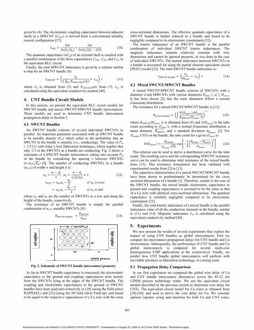
parallel. An important parameter associated with an SWCNT bundle is its metallic density (Pm) which refers to the probability that an SWCNT in the bundle is metallic (i.e., conducting). The value of Pm ≈ 1/3 [1] with today’s best fabrication techniques, which implies that only 1/3 of the SWCNTs in a bundle are conducting. Fig. 2 shows a schematic of a SWCNT bundle interconnect, taking into account Pm of the bundle by considering the spacing x between SWCNTs (x= / ) [8]. The number of conducting SWCNTs in a bundle (nCNT) of width w and height h is:
,
√3/21 12
2
1
2
where nw and nh are the number of SWCNTs in a row and along the height of the bundle, respectively.
The resistance of an SWCNT bundle is simply the parallel combination of nCNT metallic SWCNTs [8]:
13
Fig. 2. Schematic of SWCNT bundle interconnect geometry As far as SWCNT bundle capacitance is concerned, the electrostatic
capacitance to the ground and coupling capacitances arise mainly from the SWCNTs lying at the edges of the SWCNT bundle. The coupling and electrostatic capacitances to the ground of SWCNT bundles have been analyzed extensively in [10] (using the field solver RAPHAEL) and [22] (using the 3D field solver FastCap), and found to be equal to the respective capacitances of a Cu wire with the same
cross-sectional dimensions. The effective quantum capacitance of a SWCNT bundle is further reduced in a bundle and found to be negligible compared to its electrostatic counterparts [22].
The kinetic inductance of an SWCNT bundle is the parallel combination of individual SWCNT kinetic inductances. The magnetic inductance remains relatively constant with wire dimensions and cannot be ignored anymore, as was done in the case of individual SWCNTs. The mutual inductance between SWCNTs in a bundle is accounted for using the partial element equivalent circuit (PEEC) model [25]. The total SWCNT bundle inductance is:
4
. 14
4.2 Mixed SWCNT/MWCNT Bundles A mixed SWCNT/MWCNT bundle consists of SWCNTs with a
diameter d and MWCNTs with various diameters Dinner ≤ di ≤ Douter. It has been shown [2] that the outer diameters follow a normal (Gaussian) distribution.
The resistance for a mixed SWCNT/MWCNT bundle is [13]:
,
15
where RMWCNT(Douter, l) is obtained from (9) and N(Douter) is the tube count according to Douter’s, with a normal (Gaussian) distribution, a mean diameter , and a standard deviation [2]. For Nbundle CNTs in the bundle, the tube count for a given Douter is:
√2π
exp12
16
This relation can be used to derive a distribution curve for the tube count. The resulting curve and the corresponding MWCNT resistance curve can be used to determine total resistance of the mixed bundle from (15). This resistance formulation has been validated with experimental results from [2] in [13].
The capacitive characteristics of a mixed SWCNT/MWCNT bundle have been shown to predominantly be determined by the cross sectional dimensions of a bundle [1]. Therefore, similar to the case of the SWCNT bundle, the mixed bundle electrostatic capacitance to ground and coupling capacitances is assumed to be the same as that of a Cu wire with identical cross-sectional dimensions. The quantum capacitance is similarly negligible compared to its electrostatic counterparts [22].
Finally, the total kinetic inductance of a mixed bundle is the parallel inductance value of all the conduction channels in the bundle, similar to (11) and (14). Magnetic inductance Lm is calculated using the equivalent conductivity method [40]. 5. Experiments
We now present the results of several experiments that explore the impact of using CNT bundles as global interconnects. First we compare the interconnect propagation delays for CNT bundle and Cu interconnects. Subsequently, the performance of CNT bundle and Cu global interconnects is compared for several multi-core heterogeneous CMP applications at the system-level. Finally, we predict how CNT bundle global interconnects will perform with inevitable advances in fabrication technology, in coming years.
5.1 Propagation Delay Comparison In our first experiment we compared the global wire delay of Cu
and CNT bundle interconnect alternatives across the 45-22 nm UDSM process technology nodes. We use the equivalent circuit models described in the previous section to determine wire delay for CNTs. The equivalent circuit model for Cu wires is obtained from [28]-[30], and used to derive the wire delay for Cu. We consider optimal repeater sizing and insertion for both Cu and CNT wires,
Left n
eighb
or
Right neighbor
h
w st
GND plane
dt
x = dt / sqrt(Pm)
501
Authorized licensed use limited to: COLORADO STATE UNIVERSITY. Downloaded on August 22, 2009 at 14:22 from IEEE Xplore. Restrictions apply.

using the formulations presented in [31]. The node driver resistance, load capacitance and process parameters were obtained from ITRS specifications [4]. Since global wire width is typically much larger than minimum wire width (Wmin) to improve delay and bandwidth characteristics, we considered an aspect ratio of 1 and used a global wire width value of 5Wmin which is shown to optimize the power-delay product for Cu wires [32]. This wire width is in the shallow RLC region, where the difference between RC and RLC model latencies is only 10% [10]. For comparison purposes, we used the same width and aspect ratios for the SWCNT bundles and mixed SWCNT/MWCNT bundles. For the mixed SWCNT/MWCNT bundle, we assumed = 4.2nm and = 1.25nm [2]. The SWCNT diameter was assumed to be 1nm, and the ratio between outer to inner diameters for MWCNTs in the bundle was assumed to be 0.5. The spacing between adjacent wires was assumed to be the same as the wire width (5Wmin). The CNT mean free path λ = 1µm and metallic density Pm = 1/3, while Cu mean free path was assumed to be 40 nm. All of these values are practically achievable today by using prevalent fabrication techniques.
Fig. 3. Global interconnect delay comparison between Cu and CNT bundle alternatives (45-22 nm)
Fig. 3 shows the ratio of propagation delay of copper t(Cu) and the
propagation delay of CNT bundles t(CNT), for global wires (> 1mm in length) across the 45-22nm technology nodes. It can be seen that both the SWCNT bundle and mixed SWCNT/MWCNT bundle interconnects have lower propagation delays compared to Cu. The mixed SWCNT/MWCNT bundle interconnect has many large MWCNTs with several shells and more conduction channels than SWCNT bundles of the same dimensions. This is the reason why mixed SWCNT/MWCNT bundles perform better as conductors, compared to SWCNT bundles.
Fig. 4. A 4 cluster CMP layout, with global (pipelined) interconnects In addition to the comparison of propagation delays between CNT
bundle and Cu interconnects, for the sake of completeness, we also performed a comparison of the propagation delay for an isolated SWCNT global interconnect with a Cu global interconnect. The isolated SWCNT was found to have a much higher propagation delay (almost 100× more) compared to Cu. This large propagation delay is due to the very high SWCNT resistance, because of its extremely small cross-section area. We conclude from this result that isolated SWCNTs are unsuitable as global interconnects. They may however someday replace Cu at the local interconnect level because of their much lower lateral capacitance that improves latency for short
distances, as some recent studies suggest [10].
5.2 System-level Performance Analysis For our next experiment, we selected several multi-core CMP
applications to analyze the overall performance impact of using CNT bundle-based global interconnects at the system-level. The applications are selected from the well known SPLASH-2 benchmark suite (Barnes, Ocean, FFT, Radix) [33], as well as from the networking domain (proprietary benchmarks Netfilter, Datahub and SecurePck). These applications are parallelized and implemented on multiple cores. The entire chip is assumed to be partitioned into clusters (or islands) of heterogeneous computation cores. Each cluster consists of tightly coupled cores (processors, memories etc.) optimized for dedicated tasks (e.g., packet encryption, image processing, etc.) and interconnected via local bus-based Cu links that support high data bandwidths. Fig. 4 shows an example layout of a four cluster multi-core CMP. Global pipelined links (shared bus or point-to-point) are used to connect computation clusters with each other, and facilitate inter-cluster data transfers. Two clusters can be interconnected by multiple global links if higher inter-cluster bandwidth needs to be supported. Table 1 summarizes the implementation details of the CMP applications, such as number of cores (including memories, peripherals, and processors), programmable processors, computation clusters and inter-cluster global links on the chip.
Table 1. CMP Application Implementation Characteristics
CMP applications
Description cores prog. processors
clusters global links
Radix Integer radix sort 18 4 3 10 Barnes Evolution of
galaxies 26 6 4 18
FFT FFT kernel 28 6 4 12 Ocean Ocean movements 35 10 5 24
Netfilter Packet processing and forwarding
49 22 6 32 Datahub 68 26 8 34
SecurePck 94 30 8 28
The CMP applications were modeled in SystemC [35] using a fast and accurate transaction-based bus cycle accurate (T-BCA) modeling abstraction [33][34][36]. The cores in each cluster (e.g. processors, memories, peripherals) were modeled at the behavioral level granularity, while the communication at the inter- and intra-cluster level was modeled at a cycle accurate granularity. Each of the applications was simulated with testbench traffic to quickly (~few hours) and accurately estimate performance of the implementations. The various cores were interconnected using the AMBA AXI [37] standard interface protocol, with the address bus width set to 32 bits and the separate read and write data bus widths set to 64 bits.
Our analysis was performed for the 22-nm process technology node (as predicted for the 2016 node of ITRS 2005 [4]) and the interconnect fabric was clocked at frequencies ranging from 1-10 GHz to support data transfer rates in the hundreds of Gbps range for future high performance systems. The die size was assumed to be 20mm×20mm. A high level simulated annealing floorplanner based on sequence pair representation (PARQUET [38]) was used to create an early layout of the CMP application on the die, and Manhattan distance based wire routing estimates were used to determine wire lengths. For the global interconnects, in addition to repeater insertion, latch insertion is performed based on wire length, wire delay and clock frequency of the bus, to pipeline the interconnect and ensure correct operation [39]. For instance, a global Cu wire of length 10 mm has a projected delay of 2 ns in the 22-nm technology node, for a 5Wmin wire width. To support a frequency of 10 GHz (clock period of 0.1 ns), approximately 20 latches need to be inserted to ensure correct multi-cycle operation.
Fig. 5 (a) and (b) show the performance improvement (speedup in application execution time) when using SWCNT bundle and mixed
µP1 MEM
UARTIF
DMA
IO
Cluster 1 Cluster 2
Cluster 3 Cluster 4
µP1
ASIC2
µP2 µP3
GPIO IO
ASIC1MEM
Bus Matrix
Hierarchical Bus
IF MEM
MEMMEM
MEM
TIMERMEM
ASIC
DSP
GPU
IF MEM
RTCDMA
USB
MEMMEM
µP2
MEM DSP
µP1
µP2
µP3
Shared Bus
IO
Shared Bus
502
Authorized licensed use limited to: COLORADO STATE UNIVERSITY. Downloaded on August 22, 2009 at 14:22 from IEEE Xplore. Restrictions apply.
SWCNT/MWCNT bundle global interconnects, instead of Cu global interconnects, for the 22-nm technology node, with the interconnect fabric clocked at 10 GHz. Experiments with the interconnect fabric clocked at lower frequencies within the 1-10 GHz range yielded speedup results within 5% of the results shown in the figures (assuming computation core frequencies are scaled down by the same factor as the interconnect fabric), and hence the other results are not presented for brevity.
(a)
(b)
Fig. 5. System level performance speedup when using CNT bundles instead of Cu for global interconnects, assuming (a) imperfect metal-
CNT contacts, (b) perfect metal-CNT contacts
Fig. 5 (a) shows the results for the case when imperfect metal-CNT contacts are assumed. A high metal-CNT contact resistance of 100 KΩ is added to account for the excessive electron scattering at imperfect metal-CNT junctions. It can be seen that the application performance with CNT bundle global interconnects is worse than with Cu global interconnects. This is primarily an artifact of using poor metal-CNT contacts, typically constructed using Gold, Palladium or Rhodium. Many recent studies [20]-[21] with state-of-the-art fabrication techniques have however managed to reduce this contact resistance down to a very small value (a few hundred Ω). This has dramatically improved the viability of successful integration of CNTs with CMOS technology.
Fig. 5 (b) shows the application performance improvement under the assumption of perfect contacts with negligible contact resistance. The applications now perform better with CNT bundle global interconnects than with Cu global interconnects because of the lower CNT bundle interconnect delays. The lower CNT bundle delays lead to more widely spaced and hence fewer pipeline latches on global inter-cluster interconnects, resulting in global data transfers taking fewer clock cycles and improving application performance. Among the applications, Ocean can be seen to have a much smaller speedup compared to other applications. This is because Ocean has fewer inter-cluster data transfers, which reduces the advantage of having faster CNT bundle-based global interconnects. On the other hand, the speedup for Radix and FFT is lower than other applications because of the smaller length of their global interconnects, which again reduces the impact of faster CNT bundle-based global interconnects on application performance. Overall, the results indicate that SWCNT bundle global interconnects provide a speedup of up to 1.3×, while mixed bundles achieve speedups of up to 1.5×.
At first glance, these modest performance improvements over Cu
interconnects may appear to be not so significant as to justify a migration to CNT bundle interconnects. However in the next section we present results that indicate more significant CNT bundle performance gains with inevitable improvements in CNT fabrication technology.
5.3 Impact of MFP and CNT Metallic Density Our system-level experiments above assumed practical values for
CNT metallic density (Pm=1/3) and mean free path (λ=1µm) while calculating application performance gains. The modest CNT bundle speedup obtained above can be improved if breakthroughs in fabrication technology in the future allow for greater metallic density (Pm) and longer MFP lengths (λ) for CNT bundles.
Fig. 6 shows the interconnect delay speedup over Cu for SWCNT bundles and mixed SWCNT/MWCNT bundles, with increasing values of metallic density Pm, ranging from 0.3 (practical) to 1 (ideal), for a constant MFP length λ=1µm. It can be seen that there is a crossover point beyond which SWCNT bundle performance improves upon mixed SWCNT/MWCNT bundle performance. This is because as the metallic density increases, the mixed bundle has fewer metallic nanotubes than the SWCNT bundle due to large MWCNTs which prevent a tight packing. The SWCNT bundle has more tightly packed and consequently more metallic tubes which improve conductivity and performance. Fig. 7 shows a similar trend when bandwidth density of CNT bundle interconnects is compared with Cu, for varying metallic densities. It is clear from the figure that SWCNT bundle bandwidth density is superior to that of Cu for metallic densities greater than 0.3. SWCNT bundle bandwidth density also improves upon mixed SWCNT/MWCNT bundle bandwidth density for higher metallic densities, due to more tightly packed metallic tubes.
Fig. 8 and 9 show the combined performance improvement for various configurations of metallic density (Pm) and MFP (λ) lengths for the SWCNT bundle and mixed SWCNT/MWCNT bundle interconnects, respectively. It is clear from the results that increasing MFP length and metallic densities can lead to a substantial improvement in delay (and hence performance) speedup for CNT bundle interconnects – as much as 4.9× for SWCNT bundles and up to 4.4× for mixed SWCNT/MWCNT bundles. Improving CNT fabrication technology in order to achieve such performance gains is an area of tremendous research activity today [41]-[42].
6. Conclusion and Future Work
In this paper, we presented a comprehensive comparative analysis of the performance impact of using CNT bundle-based global interconnects over Cu for heterogeneous multi-core CMP applications. Our experimental results indicate that SWCNT bundles and mixed SWCNT/MWCNT bundles lead to performance gains over Cu global buses of up to 1.3× and 1.5× respectively. These gains can be further improved if the CNT mean free path (MFP) lengths and metallic densities are increased with advances in fabrication technology that are actively being explored today. Ultimately, while many manufacturing and technological factors will contribute to the realization of CNT global interconnects, our preliminary results indicate that SWCNT bundle and mixed SWCNT/MWCNT bundle based global interconnects have the properties to be viable replacements for Cu global interconnects in future high performance CMP applications, as process technology scales. Our future work will consider the impact of using CNTs as local interconnects and analyze trade-offs between CNT interconnect power, performance and bandwidth density.
Acknowledgements This research was partially supported by grants from SRC (2005-
HJ-1330 and 1617.001) and NSF (CCF-0702797).
503
Authorized licensed use limited to: COLORADO STATE UNIVERSITY. Downloaded on August 22, 2009 at 14:22 from IEEE Xplore. Restrictions apply.

Fig. 6. SWCNT bundle and mixed bundle delay speedup over Fig. 7. SWCNT bundle and mixed bundle bandwidth density Cu for varying metallic densities Pm (x-axis) speedup over Cu for varying metallic densities Pm (x-axis)
Fig. 8. SWCNT bundle speedup over Cu for different combinations Fig. 9. Mixed SWCNT/MWCNT bundle speedup over Cu for of metallic density and MFP different combinations of metallic density and MFP
References [1] A. Naeemi, et al., “On-Chip Interconnect Networks at the End of the Roadmap: Limits and Nanotechnology Opportunities”, IITC 2006. [2] J. Li, et al., “Bottom-up approach for carbon nanotube interconnects,” Appl. Phys. Lett., Apr. 2003. [3] S. M. Rossnagel, T. S. Kuan, “Alteration of Cu Conductivity in the Size Effect Regime,” JVST, Jan. 2004. [4] ITRS, International Technology Roadmap for Semiconductors, 2005. [5] M. S. Dresselhaus, et al, “Carbon nanotubes: synthesis, structure, properties, and applications”, Springer, 2001. [6] P. J. Burke, “Luttinger liquid theory as a model of the gigahertz electrical properties of carbon nanotubes,” Trans. NANO, Sep. 2002. [7] F. Kreupl, et al., “Carbon nanotubes for interconnect applications,” IEDM Tech. Dig., Dec. 2004. [8] N. Srivastava, K. Banerjee, "Performance Analysis of Carbon Nanotube Interconnects for VLSI Applications," ICCAD 2005. [9] A. Raychowdhury, K. Roy, “A circuit model for carbon nanotube interconnects: comparative study with Cu interconnects for scaled technologies”, ICCAD 2004. [10] A. Naeemi et.al, “Design and Performance Modeling for Single-Walled Carbon Nanotubes as Local, Semiglobal, and Global Interconnects in Gigascale Integrated Systems”, Trans EDL Jan 2007. [11] A. Raychowdhury, K. Roy, “Modeling of Metallic Carbon Nanotube Interconnects for Circuit Simulation and a Comparison with Cu Interconnects for Scaled Technologies,” TCAD Jan 2006. [12] A. Naeemi et al., “Performance Modeling and Optimization for Single- and Multi-Wall Carbon Nanotube Interconnects,” DAC 2007 [13] S. Haruehanroengra, W. Wang, “Analyzing Conductance of Mixed Carbon-Nanotube Bundles for Interconnect Applications”, IEEE EDL Aug 2007. [14] A. Nieuwoudt, et al., “Predicting the Performance and Reliability of Carbon Nanotube Bundles for On-Chip Interconnect,” ASPDAC, 2007. [15] B. Q. Wei, R. Vajtai, P. M. Ajayan, “Reliability and current carrying capacity of carbon nanotubes,” Appl. Phys. Lett., 2001. [16] J. Hone, et al, “Thermal conductivity of single-walled carbon nanotubes,” Phys. Rev., B, vol. 59, no. 4, 1999. [17] D. Rossi, et al., “Modeling Crosstalk Effects in CNT Bus Architectures”, IEEE Trans. NANO Mar 2007 [18] A. Nieuwoudt, Y. Massoud, “Assessing the Implications of Process Variations on Future Carbon Nanotube Bundle Interconnect Solutions,” ISQED, 2007. [19] S. Eachempati, et al., “Assessing Carbon Nanotube Bundle Interconnect for Future FPGA Architectures,” DATE, 2007. [20] S. Sato et al., “Novel approach to fabricate carbon nanotube via interconnects using size-controlled catalyst nanoparticles,” IITC 2006.
[21] O. Hjortstam, et al., "Can we achieve ultra-low resistivity in carbon nanotube-based metal composites?" App. Phy MSP 2004. [22] H. Cho, et al., “Modeling of the performance of carbon nanotube bundle, cu/low-k and optical on-chip global interconnects”, SLIP 2007. [23] S. Pasricha, and N. Dutt. “On-Chip Communication Architectures”, Morgan Kauffman, Apr 2008. [24] P. J. Burke, “Quantitative theory of nanowire and nanotube antenna performance,” ArXiv Cond. Matter E-Prints, Aug. 2004. [25] M. W. Beattie, L. T. Pileggi, “Inductance 101: Modeling and Extraction,” DAC, 2001. [26] P. G. Collins, P. Avouris, “Multishell conduction in multiwalled carbon nanotubes,” App. Phy. MSP, Mar. 2002. [27] E. R. Dobbs, Basic Electromagnetism. Chapman, Hall 1993. [28] A. F. Mayadas, M. Shatzkes, “Electrical-Resistivity Model for Polycrystalline Films: the Case of Arbitrary Reflection at External Surfaces,” Phys. Review B, vol. 1, 1970. [29] E. H. Sondheimer, “The mean free path of electrons in metals,” Adv. Physics, vol. 1, no. 1, 1952. [30] C. P. Yue, S. S. Wong, “Physical Modeling of Spiral Inductors on Silicon,” Trans. EDL, 2000. [31] Y. I. Ismail et al., “Effects of Inductance on the Propagation Delay and Repeater Insertion in VLSI Circuits” TVLSI Apr 2000. [33] S.C. Woo et al.“The SPLASH-2 programs: Characterization and methodological considerations”, ISCAS, 1995. [32] M. A. El-Moursy et al, “Optimum Wire Sizing of RLC Interconnect with Repeaters," GLSVLSI, 2003. [33] S. Pasricha, "Transaction Level Modeling of SoC with SystemC 2.0" In Proc. SNUG 2002. [34] S. Pasricha, N. Dutt, M. Ben-Romdhane, "Extending the Transaction Level Modeling Approach for Fast Communication Architecture Exploration", In Proc. DAC 2004. [35] SystemC initiative. www.systemc.org [36] W. Müller, J. Ruf,, W. Rosenstiel, “SystemC Methodologies and Applications”, Norwell, MA: Kluwer, 2003 [37] AMBA AXI Specification www.arm.com/armtech/AXI [38] S. N. Adya, I. L. Markov, "Fixed-outline Floorplanning: Enabling Hierarchical Design", IEEE Trans TVLSI, Dec. 2003 [39] V. Nookala, S. S. Sapatnekar, "Designing optimized pipelined global interconnects: Algorithms and methodology impact," ISCAS, 2005. [40] W. Wang, et al. "Inductance of mixed carbon nanotube bundles," Micro & Nano Letters, IET , vol.2, no.2, pp.35-39, June 2007 [41] Liu et al., “Densification of Carbon Nanotube Bundles for Interconnect Application”, IITC 2007 [42] Zhu et al., “Assembling Carbon Nanotube Bundles Using Transfer Process for Fine-Pitch Electrical Interconnect Applications”, EETC 2007
504
Authorized licensed use limited to: COLORADO STATE UNIVERSITY. Downloaded on August 22, 2009 at 14:22 from IEEE Xplore. Restrictions apply.