Explorer 16/32 Development Board - Conrad Electronic
56
Explorer 16/32 Development Board A Perfect Platform for Discovering the Full Capabilities of PIC® MCUs and dsPIC® DSCs Summary The Explorer 16/32 Development Board is a flexible development system for Microchip’s 16-bit and 32-bit PIC® microcontrollers. It is a refreshed and cost-effective version of Explorer 16 Development Board (DM240001) with several new features. This board supports devices from the PIC24 and PIC32 MCU families and dsPIC® DSC families as Processor Plug-In Modules (PIMs), allowing you to develop various applications quickly. The Explorer 16/32 Development Board provides a perfect platform to prototype applications using several function expansion capabilities through its wide ecosystem support. The board can be a starting point for all your embedded projects by developing a rapid proof of concept before migrating to actual design. Key Features ■ 100-pin plug-in module socket ■ Integrated PICkit™-On-Board (PKOB) Programmer/Debugger ■ MPLAB®ICD3 and MPLAB REAL ICE™ In-Circuit Debugger/Programmer support for advanced operations ■ Multiple power options • USB power for convenience • 9–15V DC supply for higher power requirement ■ Communication • USB host/device support • Serial (UART/I 2 C) communication via on-board USB-serial bridge ■ Wide ecosystem with mikroBUS™, PICtail™ Plus and Pmod™ interfaces ■ Alphanumeric LCD, push buttons, LEDs, potentiometer, temperature sensor, debug connectors and more 16-bit PIC24 MCUs and dsPIC DSCs Larger Ecosystem 32-bit PIC32 MCUs Backwards Compatible Enhanced Features What’s New in the Explorer 16/32 Development Board Classic Explorer 16 Development Board New Explorer 16/32 Development Board Device Families Supported Via PIMs PIC24, dsPIC® DSC, PIC32 PIC24, dsPIC DSC, PIC32 9–15V DC Power Supply Support ü ü PICkit™ 3, MPLAB® ICD3 and MPLAB REAL ICE™ In-Circuit Programmer/Debugger Support ü ü LCD, User LEDs, Push Buttons, Potentiometer, Temperature Sensor ü ü PICtail™ Plus Daughter Cards ü ü (Using optional PICtail Plus Expansion Board) USB Power Support – ü Integrated PICkit™-On-Board Programmer/Debugger – ü On-Board USB for Application – ü On-Board USB to Serial Communication Bridge – ü Current Measurement Capability – ü mikroBUS™ Interface and Pmod™ Footprint – ü Backwards Compatibility The new Explorer 16/32 Development Board is backwards compatible with the classic Explorer 16 Development Board in using existing codes, libraries, prototypes, PIMs and all the PICtail Plus daughter cards interfaced via the side PICtail Plus connector. Reuse the PICtail Plus daughter cards interfaced via the vertical PICtail Plus connector by using an additional PICtail Plus Expansion Board. Flexible Convenient Ready to Start
Transcript of Explorer 16/32 Development Board - Conrad Electronic

Explorer 16/32 Development BoardA Perfect Platform for Discovering the Full Capabilities of PIC® MCUs and dsPIC® DSCs
SummaryThe Explorer 16/32 Development Board is a flexible development system for Microchip’s 16-bit and 32-bit PIC® microcontrollers. It is a refreshed and cost-effective version of Explorer 16 Development Board (DM240001) with several new features. This board supports devices from the PIC24 and PIC32 MCU families and dsPIC® DSC families as Processor Plug-In Modules (PIMs), allowing you to develop various applications quickly.
The Explorer 16/32 Development Board provides a perfect platform to prototype applications using several function expansion capabilities through its wide ecosystem support. The board can be a starting point for all your embedded projects by developing a rapid proof of concept before migrating to actual design.
Key Features 100-pin plug-in module socket Integrated PICkit™-On-Board (PKOB)
Programmer/Debugger MPLAB® ICD3 and MPLAB REAL ICE™ In-Circuit
Debugger/Programmer support for advanced operations Multiple power options
• USB power for convenience• 9–15V DC supply for higher power requirement
Communication• USB host/device support• Serial (UART/I2C) communication via on-board
USB-serial bridge Wide ecosystem with mikroBUS™, PICtail™ Plus and
Pmod™ interfaces Alphanumeric LCD, push buttons, LEDs, potentiometer,
temperature sensor, debug connectors and more
16-bit PIC24 MCUs and
dsPIC DSCs
Larger Ecosystem
32-bit PIC32 MCUs
Backwards Compatible
Enhanced Features
What’s New in the Explorer 16/32 Development BoardClassic Explorer 16 Development Board
New Explorer 16/32 Development Board
Device Families Supported Via PIMs PIC24, dsPIC® DSC, PIC32 PIC24, dsPIC DSC, PIC32
9–15V DC Power Supply Support ü ü
PICkit™ 3, MPLAB® ICD3 and MPLAB REAL ICE™ In-Circuit Programmer/Debugger Support ü ü
LCD, User LEDs, Push Buttons, Potentiometer, Temperature Sensor ü ü
PICtail™ Plus Daughter Cards üü (Using optional PICtail Plus Expansion Board)
USB Power Support – ü
Integrated PICkit™-On-Board Programmer/Debugger – ü
On-Board USB for Application – ü
On-Board USB to Serial Communication Bridge – ü
Current Measurement Capability – ü
mikroBUS™ Interface and Pmod™ Footprint – ü
Backwards CompatibilityThe new Explorer 16/32 Development Board is backwards compatible with the classic Explorer 16 Development Board in using existing codes, libraries, prototypes, PIMs and all the PICtail Plus daughter cards interfaced via the side PICtail Plus connector. Reuse the PICtail Plus daughter cards interfaced via the vertical PICtail Plus connector by using an additional PICtail Plus Expansion Board.
Flexible Convenient Ready to Start

The Microchip name and logo, the Microchip logo and dsPIC, MPLAB and PIC are registered trademarks and PICkit, PICtail and REAL ICE are trademarks of Microchip Technology Incorporated in the U.S.A. and other countries. All other trademarks mentioned herein are property of their respective companies. © 2016, Microchip Technology Incorporated. All Rights Reserved. Printed in the U.S.A. 7/16DS40001854A
Visit our web site for additional product information and to locate your local sales office.Microchip Technology Inc. • 2355 W. Chandler Blvd. • Chandler, AZ 85224-6199
www.microchip.com/Explorer1632
Wide Ecosystem for All Your Application NeedsThe Explorer 16/32 Development Board provides a complete platform for all you embedded design. Designed to expand its capabilities as your needs grow, it can be operated as an all-in-one development platform or it can be customized to suit your specific needs. This can be achieved with the board’s wide ecosystem support that offer a variety of options for function expansion.
Get Started with the Explorer 16/32 Development Platform
PICtail Plus Expansion Board (AC240100)Connect vertical PICtail Plus Daughter Cards to the Explorer 16/32 Development Board using this PICtail Plus Expansion Board. This board also features a prototyping area and two mikroBUS interfaces. For more information, visit www.microchip.com/PICtailPlusExpansion.
Plug-In ModulesChoose PIMs supporting over 45 families of 16-bit MCUs and DSCs and 32-bit MCUs to explore the innovative features of the device you are interested in. For more information, please visit www.microchip.com/PIMs.
Add-On Boards via mikroBUS Interface
Add new functionality using MikroElektronika’s mikroBus connector. Interface with hundreds of plug-and-play Click™ boards supporting a range of functions. Explore the options at www.mikroe.com/click and www.mikroe.com/mikrobus.
PICtail Plus Daughter Cards
Microchip offers a range of complementary products using over 50 PICtail Plus Daughter Cards directly via the side PICtail Plus connector or the vertical PICtail Plus Connector with the additional PICtail Plus Expansion Board (AC240100). Add new functionality such as communication, graphics, audio, biometric sensor, machine-to-machine and more to your prototype. For more information, please visit www.microchip.com/PictailPlusCards.
Extensive Libraries and Code ExamplesThe Explorer 16/32 Development Board is supported by an extensive array of software libraries and code examples for quickly starting your design.
PICtail Plus Daughter Cards
Microchip offers a range of complementary products Microchip offers a range of complementary products Microchip offers a range of complementary products Microchip offers a range of complementary products
Explorer 16/32 Development Board with PIC24FJ1024GB610 PIM (DM240001-3)
This kit provides everything you need to get started with evaluation and prototype right away. The kit contains:
Explorer 16/32 Development Board
PIC24FJ1024GB610 PIM• 16-bit PIC24F superset device with USB interface and
1 MB Flash and 32 KB RAM Two USB cables (Type-C™ and micro-B cables)
For more information, visit www.microchip.com/Explorer1632.
Explorer 16/32 Development Board (DM240001-2)Get the development board and choose from a wide variety of PIMs available at www.microchip.com/PIMs. This option also serves well when migrating from the classic Explorer 16 Development Board, while the
necessary accessories like PIMs and cables are already available. For more information this development board, visit www.microchip.com/Explorer1632Board.

LCD MODULE TSB1G7000-E Version :1.0 July 29, 2008
TRULY SEMICONDUCTORS LTD. P.1
SPECIFICATION
Revision: 1.0
TSB1G7000-E This module uses ROHS material
TRULY SEMICONDUCTORS LTD: CUSTOMER:
PRODUCT : LCD MODULE
MODEL NO. : TSB1G7000-E
SUPPLIER : TRULY SEMICONDUCTORS LTD.
DATE : July 29, 2008 abcdef abcdef
CERT. No. QAC0946535 CERT. No. HKG002005 (ISO9001) (ISO14001)
Quality Assurance Department: Approved by: Technical Department:
Approved by:
If there is no special request from customer, TRULY SEMICONDUCTORS Co., Ltd will not reserve the tooling of the product under the following conditions: 1.There is no response from customer in two years after TRULY SEMICONDUCTORS Co., Ltd submit the samples; 2.There is no order in two years after the latest mass production. And correlated data (include quality record) will be reserved one year more after tooling was discarded.

LCD MODULE TSB1G7000-E Version :1.0 July 29, 2008
TRULY SEMICONDUCTORS LTD. P.2
REVISION RECORD REV NO. REV DATE CONTENTS REMARKS
1.0 2008-7-29 First Release

LCD MODULE TSB1G7000-E Version :1.0 July 29, 2008
TRULY SEMICONDUCTORS LTD. P.3
CONTENTS n GENERAL INFORMATION n EXTERNAL DIMENSIONS n ABSOLUTE MAXIMUM RATINGS n ELECTRICAL CHARACTERISTICS n TIMING OF POWER SUPPLY n ELECTRO-OPTICAL CHARACTERISTICS n INTERFACE DESCRIPTION n APPLICATION CIRCUIT n INITIAL CODE
n RELIABILITY TEST n INSPECTION CRITERION n PRECAUTIONS FOR USING LCD MODULES n USING LCD MODULES n PRIOR CONSULT MATTER n FACTORY CONTACT INFORMATION
WRITTEN BY CHECKED BY APPROVED BY
XT LIU WU JIN KUN LUO SHAN LIANG

LCD MODULE TSB1G7000-E Version :1.0 July 29, 2008
TRULY SEMICONDUCTORS LTD. P.4
n GENERAL INFORMATION
Item Contents Unit LCD type FSTN / Viewing direction 6:00 O’ Clock Glass area (W × H) 66.0 × 27.7 mm2 Viewing area (W×H) 61.0 × 15.7 mm2 Dot size (W × H) 0.55 × 0.60 mm2 Dot pitch (W × H) 0.60 × 0.65 mm2 Driver IC NT7603 / Interface Type Parallel / Input voltage 3.3 V
n EXTERNAL DIMENSIONS
(5.
20)
0.6
0.65
0.6
2.3
41.205.0
1.2
2
5.01N T7 60 3B D T- 01
0.50
12.
85MI
N
22.8
5MAX
2.50
DETAL: A
A
0.55
0.50
5.65
0.503.45
0.30
9.45±0.50
141
27.50±0.2
4-R1.00
10.
00
0.70±0.070.70±0.07
4.45
10.8
0
0.900.90
5.65
66.00±0.20
PITCH 3.45X16-0.50=54.70
1.0 MAX
27.7
0±0.2
19.7
0±0.2
8.00
15.7
0(V.A
.)
61.00(V.A.)
2.00
65.00±0.2 FRONT POLARIZER TRANSMISSIVE
65.00±0.2 REAR POLARIZER REFLECTIVE
18.7
0±0.2
FRO
NT
18.
70±
0.2
REAR
2.0MAX
PITCH1.8X13=23.40
1
2
3
4
5
6
7
8
9
10
11
12
13
14
VSS
NC
VDD
RS
R/W
E
DB0
DB1
DB2
DB3
DB4
DB5
DB6
DB7
1/3
1/16
1/5
3.3

LCD MODULE TSB1G7000-E Version :1.0 July 29, 2008
TRULY SEMICONDUCTORS LTD. P.5
84SEG76
COM14COM15COM16SEG80SEG79SEG78SEG77
83SEG75SEG74
SEG72
SEG73
~ ~
~~
~~
~~
~
DB7
OPT_LCD
COM10COM11COM12
66
67 GNDTESTDCOM9
~~
COM13 ~
SEG57
SEG58
SEG59
SEG60
SEG61
SEG62
SEG63
SEG64
SEG65
SEG66
SEG67
SEG68
SEG69
SEG70
~ ~ ~ ~ ~ ~ ~ ~
SEG42
SEG43
SEG44
SEG45
SEG46
SEG47
SEG48
SEG49
SEG50
SEG51
SEG52
SEG53
SEG54
SEG55
SEG56
~ ~ ~ ~ ~ ~ ~ ~ ~
DB4
DB0
DB0
DB2
DB2
DB5
DB4
DB5
DB6
DB6
DB5
DB4
DB0
DB6
DB1
DB1
DB2
DB1
VCC
VCC
VCC
R\W
R\W
VCC
VCC
VCC
VCC
VCC
VCC
VDD
RS
RS EE
E
R\WRS
Y
(0,0)
SEG27
SEG28
SEG29
SEG30
SEG31
SEG32
SEG33
SEG34
SEG35
SEG36
SEG37
SEG38
SEG39
SEG40
SEG41
~ ~ ~ ~ ~ ~ ~ ~
SEG13
SEG14
SEG15
SEG16
SEG17
SEG18
SEG19
SEG20
SEG21
SEG22
SEG23
SEG24
SEG25
SEG26
~ ~ ~ ~ ~ ~ ~ ~
PAD SIZE:42X90UNIT :uM
CHIP SIZE:1220X5010
~
OPT_R0
GND
OPT_R1
VCC
VCC
VCC
VCC
VCC
VCCV3
V4 V5
V5
V5
V5
NT7603BDT-01
OSC1
OSC2
VSS
V2
GND V1
GND
GND
GND
GND
GND
GND
GND
GND
GND
~
SEG11
SEG5
COM8
SEG4SEG3SEG2SEG1
COM7COM6
150
149
SEG8
SEG7
SEG9
SEG10
SEG6
~~
~~
~~
~
~~
GND
GND
GND
GND
COM4COM3COM2
166
TESTTESTM
1COM1
~~
COM5~
GND
SEG12
~
DB7
DB7
SEG71
~
Y
(0,0)
2/3
(0,0)
Y
~
SEG71
DB7
DB7
~
SEG12
GND
~ COM5
~~
COM1 1
TESTMTEST
166
COM2COM3COM4
GND
GND
GND
GND
~ ~
~~
~~
~~
~
SEG6
SEG10
SEG9
SEG7
SEG8
149150
COM6
COM7
SEG1SEG2
SEG3SEG4
COM8
SEG5
SEG11
~
GND
GND
GND
GND
GND
GND
GND
GND
GND V1
GND V2
VSS
OSC2
OSC1
NT7603BDT-01
V5
V5
V5
V5
V4
V3
VCC
VCC
VCC
VCC
VCC
VCC
OPT_R1
GND
OPT_R0
~
CHIP SIZE:1220X5010
UNIT :uM
PAD SIZE:42X90
~~~~~~~~
SEG26
SEG25
SEG24
SEG23
SEG22
SEG21
SEG20
SEG19
SEG18
SEG17
SEG16
SEG15
SEG14
SEG13
~~~~~~~~
SEG41
SEG40
SEG39
SEG38
SEG37
SEG36
SEG35
SEG34
SEG33
SEG32
SEG31
SEG30
SEG29
SEG28
SEG27
(0,0)
Y
RS
R\W E
E E
RS
RS
VDD
VCC
VCC
VCC
VCC
VCC
VCC
R\W
R\W
VCC
VCC
VCC
DB1
DB2
DB1
DB1
DB6
DB0
DB4
DB5
DB6
DB6
DB5
DB4
DB5
DB2
DB2
DB0
DB0
DB4
~~~~~~~~~
SEG56
SEG55
SEG54
SEG53
SEG52
SEG51
SEG50
SEG49
SEG48
SEG47
SEG46
SEG45
SEG44
SEG43
SEG42
~~~~~~~~
SEG70
SEG69
SEG68
SEG67
SEG66
SEG65
SEG64
SEG63
SEG62
SEG61
SEG60
SEG59
SEG58
SEG57
~COM13
~~
COM9
TESTDGND67
66
COM12COM11COM10
OPT_LCD
DB7
~~~
~~
~~
~~
SEG73
SEG72
SEG74
SEG75
83
SEG77SEG78SEG79
SEG80COM16COM15COM14
SEG7684 COM16
SEG80
COM9
SEG1
COM8
COM1
3/3
DB7
DB6
DB5
DB4
DB3
DB2DB1
DB0
ER/W
RS
VDD
NC
VSS
141

LCD MODULE TSB1G7000-E Version :1.0 July 29, 2008
TRULY SEMICONDUCTORS LTD. P.6
nABSOLUTE MAXIMUM RATINGS
Parameter Symbol Min Max Unit Supply voltage for logic VDD -0.3 7.0 V
Input voltage VIN -0.3 VDD + 0.3 V Operating temperature TOP -10 60 °C Storage temperature TST -30 70 °C
Humidity RH 90%(Max60°C) RH nELECTRICAL CHARACTERISTICS
DC CHARACTERISTICS Parameter Symbol Min Typ Max Unit
Supply voltage for logic VDD-VSS 3.2 3.3 3.4 V Input Current Idd - 0.6 1.5 mA Operating voltage for LCD VOP 3.1 3.3 3.5 V Input voltage ' H ' level VIH 0.8VDD - VDD V Input voltage ' L ' level VIL -0.3 - 0.2VDD V Output voltage ' H ' level VOH VDD -0.6 - - V Output voltage ' L ' level VOL - - 0.6 V
n TIMING OF POWER SUPPLY
PLEASE REFER TO THE DRIVER IC SPECIFICATION.

LCD MODULE TSB1G7000-E Version :1.0 July 29, 2008
TRULY SEMICONDUCTORS LTD. P.7
nELECTRO-OPTICAL CHARACTERISTICS
Item Symbol Condition Min Typ Max Unit Remark Note Response time Tr+ Tf --- 508.2 762.3 ms 2 Contrast ratio Cr 5.35 10.7 --- --- FIG4. 1 Reflectance R%
θ=30° Ta=25
--- 19.4 --- % FIG4. 4 Note 1. Contrast Ratio(CR) is defined mathematically : Contrast Ratio = LMAX
LO Where LMAX :Luminace of maximal gray level LO : Luminace of gray level 0 Note 2. Response time is the time required for the display to transition from White to black(Rise Time, Tr) and from black
to white(Decay Time, Tf). For additional information see FIG 1. The test equipment is Autronic-Melchers’s ConoScope. series
Note 3. CIE (x, y) chromaticity, The x,y value is determined by measuring luminance at each test position 1 through 5,and then make average value
Note4. For Reflectance and response time testing, the testing data is base on Autronic-Melchers’s ConoScope. Series Instruments. For contrast ratio, Surface Luminance, Luminance uniformity,CIE The test data is base on TOPCON’s BM-5 photo detector.
Photo detector
LCD panel ( MgO)
30˚
Light source
<Reflective Mode>
FIG. 4 Measuring method for optical characteristics in Reflective mode
θ

LCD MODULE TSB1G7000-E Version :1.0 July 29, 2008
TRULY SEMICONDUCTORS LTD. P.8
n INTERFACE DESCRIPTION
Pin No. Symbol Level Description 1 VSS 0V Ground 2 NC --- No connection 3 VDD +3.3V Power supply 4 RS H/L Register select signal
0: Instruction register (write), Busy flag, address counter (read) 1: Data register (write, read)
5 R/W H/L Read/Write control signal 0: Write 1: Read
6 E H/L Read/Write start signal 7 DB0 8 DB1 9 DB2 10 DB3
H/L Lower 4 tri-state bi-directional data bus for transmitting data between MPU and NT7603. Not used during 4-bit operation.
11 DB4 12 DB5 13 DB6 14 DB7
H/L Higher 4 tri-state bi-directional data bus for transmitting data between MPU and NT7603. DB7 is also used as a busy flag.
n APPLICATION CIRCUIT Please consult our technical department for detail information. n INITIAL CODE Please consult our technical department for detail information.

LCD MODULE TSB1G7000-E Version :1.0 July 29, 2008
TRULY SEMICONDUCTORS LTD. P.9
n RELIABILITY TEST
No. Test Item Test Condition Inspection after test 1 High Temperature Storage 70±2/200 hours 2 Low Temperature Storage -30±2/200 hours 3 High Temperature Operating 60±2/200 hours 4 Low Temperature Operating -10±2/200 hours
5 Temperature Cycle -10±2~25~60±2×10cycles (30min.) (5min.) (30min.)
6 Damp Proof Test 50±5×90%RH/120 hours
7 Vibration Test
Frequency:10Hz~55Hz~10Hz Amplitude:1.5mm, X,Y,Z direction for total 3hours (Packing condition)
8 Dropping test
Drop to the ground from 1m height, one time, every side of carton. (Packing condition)
9 ESD test Voltage:±4KV R: 330Ω C: 150pF
Air discharge, 5time
Inspection after 2~4hours storage at room temperature, the sample shall be free from defects: 1.Air bubble in the LCD; 2.Sealleak; 3.Non-display; 4.missing segments; 5.Glass crack; 6.Current Idd is twice higher than initial value.
Remark: 1.The test samples should be applied to only one test item. 2.Sample size for each test item is 5~10pcs. 3.For Damp Proof Test, Pure water(Resistance>10MΩ) should be used. 4.In case of malfunction defect caused by ESD damage, if it would be recovered to normal state after resetting, it
would be judge as a good part. Using ionizer(an antistatic blower) is recommended at working area in order to reduce electro-static voltage.
When removing protection film from LCM panel, peel off the tag slowly( recommended more than one second) while blowing with ionizer toward the peeling face to minimize ESD which may damage electrical circuit.
5.EL evaluation should be excepted from reliability test with humidity and temperature: Some defects such as black spot/blemish can happen by natural chemical reaction with humidity and Fluorescence EL has.
6.Please use automatic switch menu(or roll menu) testing mode when test operating mode.

LCD MODULE TSB1G7000-E Version :1.0 July 29, 2008
TRULY SEMICONDUCTORS LTD. P.10
n INSPECTION CRITERION
TRULY ® OUTGOING QUALITY STANDARD PAGE 1 OF 7
TITLE:FUNCTIONAL TEST & INSPECTION CRITERIA Mono COG Product
This spe cification is made to be used as the standard acceptance/rejection criteria for Mono COG Product. 1 sample plan Sampling plan according to GB/T2828.1-2003/ISO 2859-1: 1999 and ANSI/ASQC Z1.4-1993, normal level 2 and based on: Major defect: AQL 0.65
Minor defect: AQL 1.5 2. Inspection condition Viewing distance for cosmeetic inspection is 30cm with bare eyes, and under an environment of 800 lus(20W~40W) light intensity, all directions for inspecting the sample should be
within 45°against perpendicular line. 3. Definition of inspection zone in LCD. Zone A: character/Digit area Zone B: viewing area except Zone A (ZoneA+ZoneB=minimum Viewing area) Zone C: Outside viewing area (invisible area after assembly in customer`s product) Fig.1 Inspection zones in an LCD. Note: As a general rule, visual defects in Zone C are permissible, when it is no trouble for quality and assembly of customer`s product.
C
B A

LCD MODULE TSB1G7000-E Version :1.0 July 29, 2008
TRULY SEMICONDUCTORS LTD. P.11
TRULY ® OUTGOING QUALITY STANDARD PAGE 2 OF 7
TITLE:FUNCTIONAL TEST & INSPECTION CRITERIA Mono COG Product
4. Major Defect All functional defects such as open(or missing segment ), short and serious cosmetic defects Are classified as major defects. 5. Minor Defect Except the Major defects above, cosmetic defects such as spot, glass defect are classified as minor
defects.
Item No
Items to be inspected Inspection Standard Classification
of defects
Acceptable Qty Zone Size(mm)
A B C
Φ≤0.15 Acceptable(clutering of spot not allowed)
0.15<Φ≤0.20 1 2
0.20<Φ≤0.25 0 1
Φ>0.25 0 0
Acceptable
5.1 Spot defect (Defects in spot form,
such as dark/white
spot)
Remarks: For dark/white spot, size Φ is defined
as Φ= (X+Y) /2 y x
Minor

LCD MODULE TSB1G7000-E Version :1.0 July 29, 2008
TRULY SEMICONDUCTORS LTD. P.12
TRULY ® OUTGOING QUALITY STANDARD PAGE 3 OF 7
TITLE:FUNCTIONAL TEST & INSPECTION CRITERIA Mono COG Product
5. Cosmetic Defect
Item No
Items to be inspected Inspection Standard Classification
of defects
Size(mm) Acceptable Qty Zone
L(Length) W(Width) A、B C
L≤10.0 W≤0.01 Acceptable
L≤3.0 W≤0.03 2
L>3.0 W≤0.03 0
L≤2.5 0.03<W≤0.05 2
L>2.5 0.03<W≤0.05 0
Accep-table
W>0.05 Counted as spot defect (follows item 5.1)
5.2 Line defect (Defects in line form)
Remarks: The total of spot defect and line defect shall not exceed four.
Minor
5.3 Orientation defect (such as misalignment of L.C)
Not allowed inside viewinw area(Zone A and Zone B)
5.4 Polarizer defect
5.4.1 Polarizer Position (i) Shifting in position should not exceed the glass outline
dimension. (ii) Incomplete covering of the viewing area due to shifting is not allowed.
Minor

LCD MODULE TSB1G7000-E Version :1.0 July 29, 2008
TRULY SEMICONDUCTORS LTD. P.13
TRULY ® OUTGOING QUALITY STANDARD PAGE 4 OF 7
TITLE:FUNCTIONAL TEST & INSPECTION CRITERIA Mono COG Product
5. Cosmetic Defect
Item No
Items to be inspected Inspection Standard Classification
of defects
5.4.2 Seratches, bubble or dent on glass/polarizer/Reflector, bubble between polarizers & reflector/glass:
Acceptable Qty Zone Zize(mm)
A B C
Φ≤0.15 Acceptable
0.15<Φ≤0.20 3 5
0.20<Φ≤0.30 3 5
Φ>0.30 0 0
Acceptable
5.4 Polarizer defect
Minor
5.5 Segment deformity
5.5.1 Deformity (void or Excess) (i) void in segment Accept for A≤0.10mm (ii) Excess in segment Accept for B﹤0.02mm
(iii) Thicker and Thinner
Note: Permissible level A-B ≤0.10mm A B
Remarks: where d =segment width
Minor

LCD MODULE TSB1G7000-E Version :1.0 July 29, 2008
TRULY SEMICONDUCTORS LTD. P.14
TRULY ® OUTGOING QUALITY STANDARD PAGE 5 OF 7
TITLE:FUNCTIONAL TEST & INSPECTION CRITERIA Mono COG Product
5. Cosmetic Defect
Item No
Items to be inspected Inspection Standard Classification
of defects
5.5 Segment deformity
5.5.2 PIN Hole Acceptable if the following cases are fulfill: 0.1≤Φ≤0.25 mm acceptable MAX 5/PCS where Φ=1/2(X+Y)
Minor
5.6.1 glass protrusion (i) Maximum protrusion of outline should not exceed the maximum outline dimension in product drawing.
5.6.2 Cracks on glass is not acceptable.
Major
5.6 Glass defect
5.6.3 Chipped glass definition: r=contact pad width s=contact pab length t=glass thickness x=width of chipped area y=length of chipped area z=depth of chipped area a=dimension of glass length
Fig. 2 glass chips on LCD.
(i) Chips on contact pab(unit:mm)
X Y Z acceptable ≤0.3 ≤t/2
≤a/8 ≤0.8 ≤t
≤a/6 ≤0.5 ≤t
Minor

LCD MODULE TSB1G7000-E Version :1.0 July 29, 2008
TRULY SEMICONDUCTORS LTD. P.15
TRULY ® OUTGOING QUALITY STANDARD PAGE 6 OF 7
TITLE:FUNCTIONAL TEST & INSPECTION CRITERIA Mono COG Product
5. Cosmetic Defect
Item No
Items to be inspected Inspection Standard Classification
of defects (ii) Chips between top/bottom glass. Acceptable for chips not extend to seal part. (ii) chips inside viewing area:spot chips located inside
viewing area should be treated as spot defect. (iii) Crack on corner
X Y Z
≤5.0 ≤S/3 t
Notes: 1. Not to reach B zone 2. Target mark must be remained. 3. At least 2/3 of the electrode area should be
remained . (iv) Usual surface cracks
X Y Z Acceptable ≤0.3 T/2
≤A/6 ≤1.5 T/2
≤A/8 ≤1.0 T
5.6 Glass defect
Notes: 1. Not to reach B zone 2. The total number of the glass defect should not be more than five.
Minor

LCD MODULE TSB1G7000-E Version :1.0 July 29, 2008
TRULY SEMICONDUCTORS LTD. P.16
TRULY ® OUTGOING QUALITY STANDARD PAGE 7 OF 7
TITLE:FUNCTIONAL TEST & INSPECTION CRITERIA Mono COG Product
5. Cosmetic Defect
Item No
Items to be inspected Inspection Standard Classification
of defects
5.7 Distance between foreign
The distance between the foreign dot must exceed 30mm.
The total number of luminous dot, dart defect, contamination particle, bubble, scratch defect, pinhole must not exceed 4/piece.
5.8 Total number of
dot

LCD MODULE TSB1G7000-E Version :1.0 July 29, 2008
TRULY SEMICONDUCTORS LTD. P.17
nPRECAUTIONS FOR USING LCD MODULES
Handing Precautions (1) The display panel is made of glass and polarizer. As glass is fragile. It tends to become or chipped during handling especially on the edges. Please avoid dropping or jarring. Do not subject it to a mechanical shock by dropping it or impact. (2) If the display panel is damaged and the liquid crystal substance leaks out, be sure not to get any in your mouth. If the substance contacts your skin or clothes, wash it off using soap and water. (3) Do not apply excessive force to the display surface or the adjoining areas since this may cause the color tone to vary. Do not touch the display with bare hands. This will stain the display area and degraded insulation between terminals (some cosmetics are determined to the polarizer). (4) The polarizer covering the display surface of the LCD module is soft and easily scratched. Handle this polarizer carefully. Do not touch, push or rub the exposed polarizers with anything harder than an HB pencil lead (glass, tweezers, etc.). Do not put or attach anything on the display area to avoid leaving marks on. Condensation on the surface and contact with terminals due to cold will damage, stain or dirty the polarizer. After products are tested at low temperature they must be warmed up in a container before coming is contacting with room temperature air. (5) If the display surface becomes contaminated, breathe on the surface and gently wipe it with a soft dry cloth. If it is heavily contaminated, moisten cloth with one of the following solvents - Isopropyl alcohol - Ethyl alcohol Do not scrub hard to avoid damaging the display surface. (6) Solvents other than those above-mentioned may damage the polarizer. Especially, do not use the following. - Water - Ketone - Aromatic solvents Wipe off saliva or water drops immediately, contact with water over a long period of time may cause deformation or color fading. Avoid contacting oil and fats. (7) Exercise care to minimize corrosion of the electrode. Corrosion of the electrodes is accelerated by water droplets, moisture condensation or a current flow in a high-humidity environment. (8) Install the LCD Module by using the mounting holes. When mounting the LCD module make sure it is free of twisting, warping and distortion. In particular, do not forcibly pull or bend the I/O cable or the backlight cable. (9) Do not attempt to disassemble or process the LCD module. (10) NC terminal should be open. Do not connect anything. (11) If the logic circuit power is off, do not apply the input signals. (12) Electro-Static Discharge Control,Since this module uses a CMOS LSI, the same careful attention should be paid to electrostatic discharge as for an ordinary CMOS IC. To prevent destruction of the elements by static electricity, be careful to maintain an optimum work environment. - Before remove LCM from its packing case or incorporating it into a set, be sure the module and your body have the same electric potential. Be sure to ground the body when handling the LCD modules. - Tools required for assembling, such as soldering irons, must be properly grounded. make certain the AC power source for the soldering iron does not leak. When using an electric screwdriver to attach LCM, the screwdriver should be of ground potentiality to minimize as much as possible any transmission of electromagnetic waves produced sparks coming from the commutator of the motor. - To reduce the amount of static electricity generated, do not conduct assembling and other work under dry conditions. To reduce the generation of static electricity be careful that the air in the work is not too dried. A relative humidity of 50%-60% is recommended. As far as possible make the electric potential of your work clothes and that of the work bench the ground potential - The LCD module is coated with a film to protect the display surface. Exercise care when peeling off this protective film since static electricity may be generated (13)Since LCM has been assembled and adjusted with a high degree of precision, avoid applying excessive shocks to the module or making any alterations or modifications to it. - Do not alter, modify or change the shape of the tab on the metal frame. - Do not make extra holes on the printed circuit board, modify its shape or change the positions of components to be attached. - Do not damage or modify the pattern writing on the printed circuit board. - Absolutely do not modify the zebra rubber strip (conductive rubber) or heat seal connector. - Except for soldering the interface, do not make any alterations or modifications with a soldering iron. - Do not drop, bend or twist LCM.

LCD MODULE TSB1G7000-E Version :1.0 July 29, 2008
TRULY SEMICONDUCTORS LTD. P.18
Handling precaution for LCM LCM is easy to be damaged. Please note below and be careful for handling. Correct handling: Incorrect handling:
Please don’t hold the surface of panel.
Please don’t touch IC directly. Please don’t stack LCM.
Please don’t hold the surface of IC. Please don’t operate with sharp stick such as pens.
Please don’t stretch interface of output, such as FPC cable.
As above picture, please handle with anti-static gloves around LCM edges.

LCD MODULE TSB1G7000-E Version :1.0 July 29, 2008
TRULY SEMICONDUCTORS LTD. P.19
Storage Precautions When storing the LCD modules, the following precaution is necessary. (1) Store them in a sealed polyethylene bag. If properly sealed, there is no need for the dessicant. (2) Store them in a dark place. Do not expose to sunlight or fluorescent light, keep the temperature between 0°C and 35°C, and keep the relative humidity between 40%RH and 60%RH. (3) The polarizer surface should not come in contact with any other objects. (We advise you to store them in the anti-static electricity container in which they were shipped. Others Liquid crystals solidify under low temperature (below the storage temperature range) leading to defective orientation or the generation of air bubbles (black or white). Air bubbles may also be generated if the module is subject to a low temperature. If the LCD modules have been operating for a long time showing the same display patterns, the display patterns may remain on the screen as ghost images and a slight contrast irregularity may also appear. A normal operating status can be regained by suspending use for some time. It should be noted that this phenomenon does not adversely affect performance reliability. To minimize the performance degradation of the LCD modules resulting from destruction caused by static electricity etc., exercise care to avoid holding the following sections when handling the modules. - Exposed area of the printed circuit board.
-Terminal electrode sections. n USING LCD MODULES Installing LCD Modules The hole in the printed circuit board is used to fix LCM as shown in the picture below. Attend to the following items when installing the LCM. (1) Cover the surface with a transparent protective plate to protect the polarizer and LC cell.
(2) When assembling the LCM into other equipment, the spacer to the bit between the LCM and the fitting plate should have enough height to avoid causing stress to the module surface, refer to the individual specifications for measurements. The measurement tolerance should be ±0.1mm. Precaution for assemble the module with BTB connector: Please note the position of the male and female connector position, don’t assemble or assemble like the method which the following picture shows
OK NG

LCD MODULE TSB1G7000-E Version :1.0 July 29, 2008
TRULY SEMICONDUCTORS LTD. P.20
Precaution for soldering the LCM
Manual soldering Machine drag soldering Machine press soldering
No ROHS product
290°C ~350°C. Time : 3-5S.
330°C ~350°C. Speed : 4-8 mm/s.
300°C ~330°C. Time : 3-6S. Press: 0.8~1.2Mpa
ROHS product
340°C ~370°C. Time : 3-5S.
350°C ~370°C. Time : 4-8 mm/s.
330°C ~360°C. Time : 3-6S. Press: 0.8~1.2Mpa
(1) If soldering flux is used, be sure to remove any remaining flux after finishing to soldering operation. (This does
not apply in the case of a non-halogen type of flux.) It is recommended that you protect the LCD surface with a cover during soldering to prevent any damage due to flux spatters. (2) When soldering the electroluminescent panel and PC board, the panel and board should not be detached more than three times. This maximum number is determined by the temperature and time conditions mentioned above, though there may be some variance depending on the temperature of the soldering iron. (3) When remove the electroluminescent panel from the PC board, be sure the solder has completely melted, the soldered pad on the PC board could be damaged. Precautions for Operation (1) Viewing angle varies with the change of liquid crystal driving voltage (VLCD). Adjust VLCD to show the best contrast. (2) It is an indispensable condition to drive LCD's within the specified voltage limit since the higher voltage then the limit cause the shorter LCD life. An electrochemical reaction due to direct current causes LCD's undesirable deterioration, so that the use of direct current drive should be avoided. (3) Response time will be extremely delayed at lower temperature than the operating temperature range and on the other hand at higher temperature LCD's show dark color in them. However those phenomena do not mean malfunction or out of order with LCD's, Which will come back in the specified operating temperature. (4) If the display area is pushed hard during operation, the display will become abnormal. However, it will return to normal if it is turned off and then back on. (5) A slight dew depositing on terminals is a cause for electro-chemical reaction resulting in terminal open circuit. Usage under the maximum operating temperature, 50%RH or less is required.
(6) Input logic voltage before apply analog high voltage such as LCD driving voltage when power on. Remove analog high voltage before logic voltage when power off the module. Input each signal after the positive/negative voltage becomes stable. (7) Please keep the temperature within specified range for use and storage. Polarization degradation, bubble generation or polarizer peel-off may occur with high temperature and high humidity.
Safety (1) It is recommended to crush damaged or unnecessary LCDs into pieces and wash them off with solvents such as acetone and ethanol, which should later be burned. (2) If any liquid leaks out of a damaged glass cell and comes in contact with the hands, wash off thoroughly with soap and water. Limited Warranty Unless agreed between TRULY and customer, TRULY will replace or repair any of its LCD modules which are found to be functionally defective when inspected in accordance with TRULY LCD acceptance standards (copies available upon request) for a period of one year from date of production. Cosmetic/visual defects must be returned to TRULY within 90 days of shipment. Confirmation of such date shall be based on data code on product. The warranty liability of TRULY limited to repair and/or replacement on the terms set forth above. TRULY will not be responsible for any subsequent or consequential events. Return LCM under warranty No warranty can be granted if the precautions stated above have been disregarded. The typical examples of violations are : - Broken LCD glass. - PCB eyelet is damaged or modified. - PCB conductors damaged. - Circuit modified in any way, including addition of components. - PCB tampered with by grinding, engraving or painting varnish. - Soldering to or modifying the bezel in any manner.

LCD MODULE TSB1G7000-E Version :1.0 July 29, 2008
TRULY SEMICONDUCTORS LTD. P.21
Module repairs will be invoiced to the customer upon mutual agreement. Modules must be returned with sufficient description of the failures or defects. Any connectors or cable installed by the customer must be removed completely without damaging the PCB eyelet, conductors and terminals. n PRIOR CONSULT MATTER
1.①For Truly standard products, we keep the right to change material, process ... for improving the product property without notice on our customer.
For OEM products, if any change needed which may affect the product property, we will consult ②with our customer in advance.
2.If you have special requirement about reliability condition, please let us know before you start the test on our samples.
n FACTORY
FACTORY NAME: TRULY SEMICONDUCTORS LTD. FACTORY ADDRESS: Truly Industrial Area, ShanWei City,GuangDong,China P.C: 516600 URL: http://www.truly.com.hk http://www.trulysemi.com


NT7603
Single-Chip 16C X 2L Dot-Matrix LCD Controller / Driver
1 V2.3
Features ! Internal LCD drivers
16 common signal drivers 80 segment signal drivers ! Maximum display dimensions
16 characters X 2 lines or 32 characters X 1 line
! Interfaces with 4-bit or 8-bit MPU ! Versatile display functions provided on chip:
Display Clear, Cursor Home, Display ON/OFF, Cursor ON/OFF, Character Blinking, Cursor Shift, and Display Shift
! Three duty factors, selected by PROGRAM: 1/8, 1/11, and 1/16
! Displays Data RAM (DD RAM): 80 X 8 bits (Displays up to 80 characters)
! Character Generator RAM (CG RAM): 64 X 8 bits for general data, 8 5 X 8 programmable dot patterns, or 4 5 X 10 programmable dot patterns
! Low voltage reset ! ITO option for A-type and B-type LCD waveform
! Character Generator ROM (CG ROM): 2 kinds of CG ROM sizes: 192 characters: 160 5 X 8 dot patterns 32 5 X 10 dot patterns 240 characters:
192 5 X 8 dot patterns 48 5 X 10 dot patterns
Custom CG ROM is also available ! Built-in power-on reset function ! Logic power supply: 2.8V ~ 5.5V ! LCD driver power supply: V1 ~ V5
(VDD + 0.3 - VDD - 7.0), divided by Built-in LCD power division resister.
! Two oscillator operations (Freq. = 500KHz - 540KHz): • Built-in RC oscillation • External clock ! CMOS Process ! Available in COG FORM
General Description The NT7603 is a dot matrix LCD controller and driver LSI that can operate with either a 4-bit or an 8-bit microprocessor (MPU). The NT7603 receives control character codes from the MPU, stores them in an internal RAM (up to 80 characters) before transforming each character code into a 5 X 7, 5 X 8, or 5 X 10 dot matrix character pattern and then displaying the codes on the LCD panel. The built-in Character Generator ROM consists of 256 different character patterns.
The NT7603 also contains Character Generator RAM where the user can store 8 different character patterns at run time. These memory features make the character display flexible. NT7603 also provides many display instructions to achieve versatile LCD display functions. The NT7603 is fabricated on a single LSI chip using the CMOS process, resulting in very low power requirements.
NT7603
2 V2.3
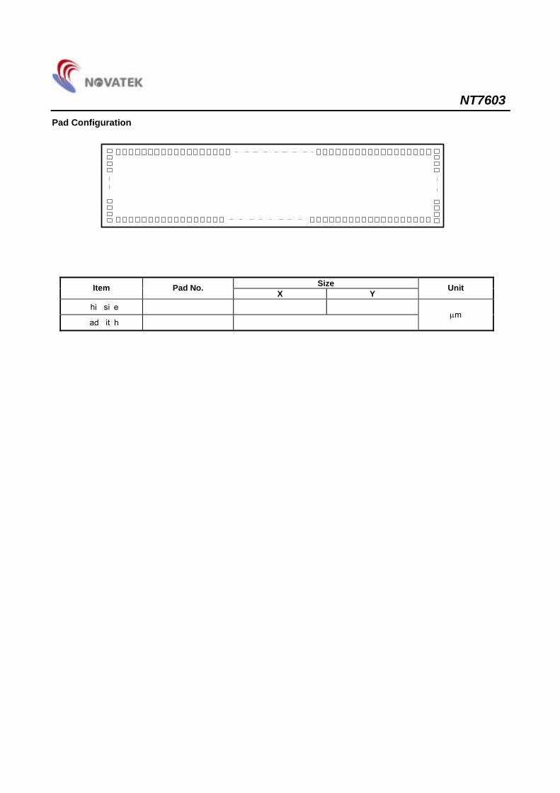
Pad Configuration
1 66
67
83
84
150
149
166
Size Item Pad No. X Y
Unit
Chip size - 5156 1349
Pad pitch 1 - 166 70 µm

NT7603
3 V2.3
Block Diagram
I/OBUFFER
V1V2V3V4V5
RS
R/W
E
DB7 ~ DB4
DB3 ~ DB0
4
4
INSTRUCTIONREGISTER
(IR)
8
INSTRUCTIONDECODE8
ADDRESSCOUNTER
VDD
GNDOSC1OSC2
TIMINGGENERATOR
DATAREGISTER
(DR)
BUSYFLAG(BF)
8
7
7
CHARACTERGENERATOR
RAM(CG RAM)
64 X 8 BITS
CURSORADDRESSCOUNTER
DISPLAYDATARAM
(DD RAM)80 X 8 BITS
16-BITSHIFT
REGISTER
COMMONSIGNALDRIVER
7
CURSOR/BLINK
CONTROLLER
77
7
LCD DRIVERVOLTAGE
GENERATOR
16
8
8
CHARACTERGENERATOR
ROM (CG ROM)
8
16 COM1I
COM16
80-BITLATCH
CIRCUIT
SEGMENTSIGNALDRIVER
80 80 SEG1I
SEG80
PARALLER - TO - SERIALCONVERTER
55
TESTM
7
OPT_R0OPT_R1OPT_LCD
TEST
TESTD

NT7603
4 V2.3
Pad Description (Total 166 pads for COG type)
Pad No. Designation I/O External Connection Description
1 - 15 GND P Power supply GND: 0V
16 OSC1 I For external clock operation, clock inputs to OSC1
17 OSC2 O Clock output
18 V1 P Power supply Power supply for LCD driver. VDD ≥ V1 ≥ V2 ≥ V3 ≥ V4 ≥ V5 ≥ GND
19 V2 P Power supply Power supply for LCD driver
20 V3 P Power supply Power supply for LCD driver
21 V4 P Power supply Power supply for LCD driver
22 - 25 V5 P Power supply Power supply for LCD driver
26, 28 OPT_R0, OPT_R1
I ITO Option
The built-in bias resister select: OPT_R1, OPT_R0: No ITO = 1. ITO on = 0 1, 1: 2.2KΩ; 1, 0: 4KΩ; 0, 1: 6.8KΩ; 0, 0:No built-in bias resistor
29 - 43 VDD P Power supply VDD: +5V
44, 45 RS I MPU Register select signal 0: Instruction register (write), Busy flag, address counter (read) 1: Data register (write, read)
46, 47 R/W I MPU Read/Write control signal 0: Write 1: Read
48, 49 E I MPU Read/Write start signal
50, 51 DB0
52, 53 DB1
54, 55 DB2
56, 57 DB3
I/O MPU Lower 4 tri-state bi-directional data bus for transmitting data between MPU and NT7603. Not used during 4-bit operation.
58, 59 DB4
60, 61 DB5
62, 63 DB6
64, 65 DB7
I/O MPU Higher 4 tri-state bi-directional data bus for transmitting data between MPU and NT7603. DB7 is also used as a busy flag.
66 OPT_LCD I ITO Option No ITO. (Option = 1): B-Type waveform ITO On. (Option = 0): A-Type waveform
68 TESTD O Test output Test data output. (No connect for user)
164 - 157 COM1 - 8 O LCD panel
69 - 76, COM9 - 16 O LCD panel Common signal output pins, for place on the upper glass (IC face up)
156 - 77 SEG1 - 80 O LCD panel Segment signal output pins
165 TEST I Test pin Test pin (internal pull down) (No connection for user)
166 TESTM O Test output LCD driver clock output. (No connection for user)
67, 27 GND_OUT P GND output pin, used for pull-down ITO option

NT7603
5 V2.3
Functional Description The NT7603 is a dot-matrix LCD controller and driver LSI. It operates with either a 4-bit or an 8-bit microprocessor (MPU). The NT7603 receives both instructions and data from the MPU. Some instructions set operation modes, such as the function mode, data entry mode, and display mode; as well as some control LCD display functions, such as clear display, restore display, shift display, and cursor. Other instructions include reading and writing both data and addresses. All instructions allow users convenient and powerful functions to control the LCD dot-matrix displays. Data is written into, and read from the Data Display RAM (DD RAM) or the Character Generator RAM (CG RAM). As display character codes, the data stored in the DD RAM decodes a set of dot-matrix character patterns that are built into the Character Generator ROM (CG ROM). The CG ROM, with many character patterns (up to 256 patterns), defines the character pattern fonts. The NT7603 regularly scans the character patterns through the segment drivers. The CG RAM stores character pattern fonts at run time if users intend to show character patterns that are not defined in the CG ROM. This feature makes character display flexible. Other unused bytes can be used as general-purpose data storage. The LCD driver circuit consists of 16 common signal drivers and 80 segment signal drivers allowing a variety of application configurations to be implemented. Character Generator ROM (CG ROM) The character generator ROM generates LCD dot character patterns from the 8-bit character pattern codes. The NT7603 provides 2 CG ROM configurations:
1. 192 Characters: The CG ROM contains 160 5 X 8 dot character patterns and 32 5 X 10 dot character patterns. The relation between the character codes and character patterns is shown in Table 1. The character codes from 00H to 0FH are used to get character patterns from the CG RAM. Character codes from 10H to 1FH, from 80H to 9FH and 20H map to null character patterns. Character codes from E0H to FFH are assigned to generate 5 X 10 dot character patterns, and other codes are used to generate 5x8 dot character patterns. 2. 240 Characters: The CG ROM contains 192 5 X 8 dot character patterns and 48 5 X 10 dot character patterns. The relation between the character codes and character patterns is shown in Table 2. The character codes from 00H to 0FH are used to get character patterns from the CG RAM. Character codes from 10H to 1FH and from E0H to FFH are assigned to generate 5 X 10 dot character patterns, and other codes to generate 5 X 8 dot character patterns. Only one null character pattern exists in this type. Note that the underlined cursor, displayed on the 8th duty may be obscure if the 8th row of a dot character pattern is coded. We recommend that users display the cursor in the blinking mode if they code 5x8 dot character patterns as their custom CG ROM. Custom character patterns are available by mask-programming ROM. For convenience of character pattern development, NOVATEK has developed a user-friendly editor program for the NT7603 to help determine the character patterns users prefer. By executing the program on the computer, users can easily create and modify their character patterns. By transferring the resulting files generated by the program through a modem or some other communication method, the user and NOVATEK will have established a reliable, fast link for programming the CG ROM.

NT7603
6 V2.3
Absolute Maximum Ratings* Power Supply Voltage (VDD) . . . . . . . . . . -0.3V to + 7.0V Power Supply Voltage (V1 to V5) . . . . . . . . . . . . . . . . . . . . . . . . . . . . . . . . . . . . . . . . . . . . . . . . GND to VDD + 0.3V Input Voltage (VI) . . . . . . . . . . . . . . . -0.3V to VDD + 0.3V Operating Temperature (TOPR) . . . . . . .-20°C to + 70°C Storage Temperature (TSTG) . . . . . . . .-55°C to + 125°C
*Comments Stresses above those listed under "Absolute Maximum Ratings" may cause permanent damage to this device. These are stress ratings only. Functional operation of this device at these or any other conditions above those indicated in the operational sections of this specification is not implied or intended. Exposure to the absolute maximum rating conditions for extended periods may affect device reliability.
! All voltage values are referenced to GND = 0V ! V1 to V5, must maintain VDD ≥ V1 ≥ V2 ≥ V3 ≥ V4 ≥ V5 ≥ GND
DC Electrical Characteristics (VDD = 5.0V, GND = 0V, TA = 25°C)
Symbol Parameter Min. Typ. Max. Unit Conditions Applicable Pin
VDD Operating Voltage 2.8 5.0 5.5 V
VIH1 "H" Level Input Voltage (1) 0.8 VDD - VDD V DB0 - DB7, RS, R/W,
VIL1 "L" Level Input Voltage (1) -0.3 - 0.2 VDD V E,OSC1
VOH1 "H" Level Output Voltage (1) VDD - 0.6 - - V IOH = -1.2mA DB0 - DB7
VOL1 "L" Level Output Voltage (1) - - GND + 0.6 V IOL = 1.2mA (CMOS)
VCOM Driver Voltage Descending (COM) - - 0.3 V ID = 5µA COM1 - 16
VSEG Driver Voltage Descending (SEG) - - 0.3 V ID = 5µA SEG1 - 80
IIL Input Leakage Current -1 - 1 µA VIN = 0 to VDD Not include OSC1
-IP Pull-up MOS Current 50 125 250 µA VDD = 5V RS, R/W, DB0-DB7
IOP Power Supply Current - 1 1.5 mA
Rf oscillation, from external
clock VDD = 5V, fOSC = fCP =
540KHz, include LCD bias current.
VDD
External Clock Operation
fCP External Clock Operating Frequency 380 540 750 KHz
tDUTY External Clock Duty Cycle 45 50 55 %
tRCP External Clock Rising Time 0.1 - 0.5 µS
tFCP External Clock Falling Time 0.1 - 0.5 µS
Internal Clock Operation (Built-in RC Oscillator)
fOSC Oscillator Frequency 380 540 750 KHz VDD = 2 .8V ~ 5.5V
VLCD LCD Driving Voltage 3.0 - VDD V VDD - V5

NT7603
7 V2.3
DC Electrical Characteristics (continued) (VDD = 3.0V, GND = 0V, TA = 25°C)
Symbol Parameter Min. Typ. Max. Unit Conditions Applicable Pin
VDD Operating Voltage 2.8 3.0 5.5 V
VIH1 "H" Level Input Voltage (1) 0.8 VDD - VDD V DB0 - DB7, RS, R/W,
VIL1 "L" Level Input Voltage (1) -0.3 - 0.2 VDD V E,OSC1
VOH1 "H" Level Output Voltage (1) VDD - 0.4 - - V IOH = -0.8mA DB0 - DB7
VOL1 "L" Level Output Voltage (1) - - GND + 0.4 V IOL = 0.8mA (CMOS)
VCOM Driver Voltage Descending (COM) - - 0.3 V ID = 5µA COM1 - 16
VSEG Driver Voltage Descending (SEG) - - 0.3 V ID = 5µA SEG1 - 80
IIL Input Leakage Current -1 - 1 µA VIN = 0 to VDD Not include OSC1
-IP Pull-up MOS Current 30 75 150 µA VDD = 3V RS, R/W, DB0-DB7
IOP Power Supply Current - 1 1.5 mA
Rf oscillation, from external clock VDD =
3.0V, fOSC = fCP =
540KHz, include LCD bias current.
VDD
External Clock Operation
fCP External Clock Operating Frequency 380 540 750 KHz
tDUTY External Clock Duty Cycle 45 50 55 %
tRCP External Clock Rising Time 0.1 - 0.5 µS
tFCP External Clock Falling Time 0.1 - 0.5 µS
Internal Clock Operation (Built-in RC Oscillator)
fOSC Oscillator Frequency 380 540 750 KHz Rf = 50KΩ (reference only) VDD = 2 .8V ~ 5.5V
VLCD LCD Driving Voltage 2.5 - VDD V VDD - V5

NT7603
8 V2.3
AC Characteristics
Read Cycle (VDD = 5.0V, GND = 0V, TA = 25°C)
Symbol Parameter Min. Typ. Max. Unit Conditions
tCYCE Enable Cycle Time 500 - - ns Figure 1
tWHE Enable "H" Level Pulse Width 300 - - ns Figure 1
tRE, tFE Enable Rising/Falling Time - - 25 ns Figure 1
tAS RS, R/W Setup Time 601 - - ns Figure 1
1002
tAH RS, R/W Address Hold Time 10 - - ns Figure 1
tRD Read Data Output Delay - - 190 ns Figure 1
tDHR Read Data Hold Time 20 - - ns Figure 1 Write Cycle (VDD = 5.0V, GND = 0V, TA = 25°C)
Symbol Parameter Min. Typ. Max. Unit Conditions
tCYCE Enable Cycle Time 500 - - ns Figure 2
tWHE Enable "H" Level Pulse Width 300 - - ns Figure 2
tRE, tFE Enable Rising/Falling Time - - 25 ns Figure 2
tAS RS, R/W Setup Time 601 - - ns Figure 2
1002
tAH RS, R/W Address Hold Time 10 - - ns Figure 2
tDS Data Output Delay 100 - - ns Figure 2
tDHW Data Hold Time 10 - - ns Figure 2
Notes: 1: 8-bit operation mode 2: 4-bit operation mode
Power Supply Conditions Using Internal Reset Circuit
(VDD = 5.0V, GND = 0V, TA = 25°C)
Symbol Parameter Min. Typ. Max. Unit Conditions
tRON Power Supply Rising Time 0.1 - 10 ms Figure 3
tOFF Power Supply OFF Time 1 - - ms Figure 3

NT7603
9 V2.3
AC Characteristics (continued)
Read Cycle (VDD = 3.0V, GND = 0V, TA = 25°C)
Symbol Parameter Min. Typ. Max. Unit Conditions
tCYCE Enable Cycle Time 500 - - ns Figure 1
tWHE Enable "H" Level Pulse Width 300 - - ns Figure 1
tRE, tFE Enable Rising/Falling Time - - 25 ns Figure 1
tAS RS, R/W Setup Time 601 - - ns Figure 1
1002
tAH RS, R/W Address Hold Time 10 - - ns Figure 1
tRD Read Data Output Delay - - 190 ns Figure 1
tDHR Read Data Hold Time 20 - - ns Figure 1 Write Cycle (VDD = 3.0V, GND = 0V, TA = 25°C)
Symbol Parameter Min. Typ. Max. Unit Conditions
tCYCE Enable Cycle Time 500 - - ns Figure 2
tWHE Enable "H" Level Pulse Width 300 - - ns Figure 2
tRE, tFE Enable Rising/Falling Time - - 25 ns Figure 2
tAS RS, R/W Setup Time 601 - - ns Figure 2
1002
tAH RS, R/W Address Hold Time 10 - - ns Figure 2
tDS Data Output Delay 150 - - ns Figure 2
tDHW Data Hold Time 10 - - ns Figure 2
Notes: 1: 8-bit operation mode 2: 4-bit operation mode
Power Supply Conditions Using Internal Reset Circuit
(VDD = 3.0V, GND = 0V, TA = 25°C)
Symbol Parameter Min. Typ. Max. Unit Conditions
tRON Power Supply Rising Time 0.1 - 10 ms Figure 3
tOFF Power Supply OFF Time 1 - - ms Figure 3

NT7603
10 V2.3
Timing Waveforms Read Operation
RS
R/W
E
DB0 ~ DB7
VIH1
VIL1tRE
tRD
VOH1VOL1 VAILD DATA
VIH1
VIL1
tAS
VIH1
VIL1
tAH
tWHEtFE
VIL1
tDHR
VOH1VOL1
tCYCE
VIL1
Figure 1. Bus Read Operation Sequence
(Reading out data from NT7603 to 8-bit MPU)
Write Operation
RS
R/W
E
DB0 ~ DB7
VIH1
VIL1tRE
tDS
VIH1VIL1 VAILD DATA
VIH1
VIL1
tAS
VIH1
VIL1
tAH
tWHEtFE
VIL1
tDHW
VIH1VIL1
tCYCE
VIL1
VIL1
Figure 2. Bus Write Operation Sequence
(Writing data from 8-bit MPU to NT7603)
Interface Signals with Segment Driver LSI
VDD0.2V
tRON
4.5V
0.1ms > tRON > 10mstOFF
0.2V0.2V
tOFF > 1ms
Figure 3. tOFF stipulates the time of power OFF for instantaneous Power supply to or when power supply repeats ON and OFF

NT7603
11 V2.3
Note 1: The NT7603 has two clock options: A. Internal Oscillator (Built-in RC)
OSC1 OSC2
OPENOPEN
B. External Clock Operation
OSC1 OSC2
OPENPULSE INPUT
Note 2: Input/Output Terminals: A. Input Terminal
Applicable Terminal: E (No Pull Up MOS)
PMOS
VDD
NMOS
Applicable Terminal: RS, R/W (with Pull Up MOS)
PMOS
VDD
NMOS
VDD
PMOS
Pull Up MOS

NT7603
12 V2.3
B. Output Terminal
Applicable Terminal: TESTM
PMOS
VDD
NMOS
C I/O Terminal
Applicable Terminal: DB0 to DB7
NMOS
VDD
PMOS
Pull Up MOS
PMOS
VDD
PMOS
VDD
NMOS
ENABLE
DATA
(OUTPUT CIRCUIT)(TRISTATE)
Note 3: ITO Options: Set Option = 0: Place ITO on the Option Pad Set Option = 1: No ITO on the Option Pad
GND_OUT
OPTION PAD
OPTION(Internalpull up)
Option = 1
No ITO:
OPTION PAD
ITO On:
ITO
Option = 0
OPTION(Internalpull up)
GND OUTPUTPAD
GND OUTPUTPAD
GND_OUT

NT7603
13 V2.3
Table 1. NT7603H-BDT01 Correspondence between Character Codes and Character Patterns (NOVATEK Standard 192 Character CG ROM)

NT7603
14 V2.3
Instruction Set
Code Function Executiontime (max)Instruction
RS RW DB7 DB6 DB5 DB4 DB3 DB2 DB1 DB0 (fOSC = 540KHz)
Display Clear 0 0 0 0 0 0 0 0 0 1
Clear entire display area, Restore display from shift, and load address counter with DD RAM address 00H.
1.64ms
Display/ Cursor Home 0 0 0 0 0 0 0 0 1 *
Restore display from shift and load address counter with DD RAM address 00H.
1.64ms
Entry Mode Set 0 0 0 0 0 0 0 1 I/D S
Specify direction of cursor movement and display shift mode. This operation takes place after each data transfer (read/write).
40µs
Display ON/OFF 0 0 0 0 0 0 1 D C B
Specify activation of display (D) cursor (C) and blinking of character at cursor position (B).
40µs
Display/ Cursor Shift 0 0 0 0 0 1 S/C R/L * * Shift display or move cursor. 40µs
Function Set 0 0 0 0 1 DL N F * * Set interface data length (DL), number of display line (N), and character font (F).
40µs
RAM Address Set 0 0 0 1 ACG
Load the address counter with a CG RAM address. Subsequent data access is for CG RAM data.
40µs
DD RAM Address Set 0 0 1 ADD
Load the address counter with a DD RAM address. Subsequent data access is for DD RAM data.
40µs
Busy Flag/ Address Counter Read
0 1 BF AC Read Busy Flag (BF) and contents of Address Counter (AC).
1µs
CG RAM/ DD RAM Data Write
1 0 Write data Write data to CG RAM or DD RAM. 40µs
CG RAM/ DD RAM Data Read
1 1 Read data Read data from CG RAM or DD RAM. 40µs
I/D = 1 : Increment I/D = 0 : Decrement S = 1 : Display Shift On D = 1 : Display On C = 1 : Cursor Display On B = 1 : Cursor Blink On S/C = 1 : Shift Display S/C = 0 : Move Cursor R/L = 1 : Shift Right R/L = 0 : Shift Left DL = 1 : 8-Bit DL = 0 : 4-Bit N = 1 : Dual Line N = 0 : Signal Line F = 1 : 5x10 dots F = 0 : 5 X 8 dots BF = 1 : Internal Operation BF = 0 : Ready for Instruction
DD RAM : Display Data RAM CG RAM : Character Generator RAM ACG : Character Generator RAM Address ADD : Display Data RAM Address AC : Address Counter
Note 1: Symbol "*" signifies an insignificant bit (disregard). Note 2: Correct input value for "N" is predetermined for each model. Note 3: The variation of execution time depends on the change of oscillator frequency; for example:
if fOSC = 380KHz, then execution time = 40µs× (540KHz / 380KHz) = 57µs

NT7603
15 V2.3
Interface to LCD (1) Character Font and Number of Lines The NT7603 provides a 5 X 7 dot character font 1-line mode, a 5 X 10 dot character font 1-line mode and a 5 X 7 dot character font 2-line mode, as shown in the table below.
Three types of common signals are available as displayed in the table. The number of lines and the font type can be selected by the program.
Number of Lines Character Font Number of Common Signals Duty Factor Bias
1 5 X 7 dots + Cursor (or 5 X 8 dots)
8 1/8 1/4
1 5 X 10 dots + Cursor 11 1/11 1/4
2 5 X 7 dots + Cursor (or 5 X 8 dots)
16 1/16 1/5
(2) Connection to LCD
The following 4 LCD connection examples show the various combinations between characters and lines. NT7603 can directly drive the following combinations:
(a) 5 X 8 Font - 16 character X 1 line (1/8 duty cycle, 1/4 bias)
NT7603
COM1
COM8
SEG1
SEG80
LCD PANEL

NT7603
16 V2.3
(b) 5 X 10 Font - 16 character X 1 line (1/11 duty cycle, 1/4 bias)
NT7603
COM1
COM8
SEG1
SEG80
LCD PANEL
COM11
COM9
(c) 5 X 8 Font - 16 character X 2 line (1/16 duty cycle, 1/5 bias)
NT7603
COM1
COM8
SEG1
SEG80
LCD PANEL
COM16
COM9

NT7603
17 V2.3
(d) 5 X 8 Font - 32 character X 1 line (1/16 duty cycle, 1/5bias)
NT7603
COM1
COM8
SEG1
SEG80
LCD PANEL
COM16
COM9
(3) Orientation type of NT7603:
Place the chip on the upper glass (IC face up)
NT76031
LCD PANEL
C1, S1
C16, S80
C8, S1
C9, S80

NT7603
18 V2.3
(4) Bias Power Connection
NT7603 provides 1/4 or 1/5 bias for various duty cycle applications. The built-in power division resistor divide voltage is described in the following table. The division resistor is the connection of the NT7603, power supply, and resistors are also shown as follows:
Power Division 1/8, 1/11 Duty Cycle - 1/4 Bias 1/16 Duty Cycle - 1/5 Bias
V1 VDD - 1/4 VLCD VDD - 1/5 VLCD
V2 VDD - 1/2 VLCD VDD - 2/5 VLCD
V3 VDD - 1/2 VLCD VDD - 3/5 VLCD
V4 VDD - 3/4 VLCD VDD - 4/5 VLCD
V5 VDD - VLCD VDD - VLCD
The bias is auto selected by duty cycle. When the LCD is set to 1/16 duty, the bias is set to 1/5. Otherwise, the bias is set to 1/4. The ITO Option can then select the division resistor value:
OPT_R1 OPT_R0 Division Resister
No ITO (1) No ITO (1) 2.2KΩ
No ITO (1) ITO On (0) 4KΩ
ITO On (0) No ITO (1) 6.8KΩ
ITO On (0) No ITO (0) No built-in resister(external input)
NT7603
VDD
V1
V2
V3
V4
V5
VDD
VR
GND
VLCD
Built-in bias resister2.2K,4K or 6.8K ohm.
NT7603
VDD
V1
V2
V3
V4
V5
VR
GND
VDD
R
R
R
R
VLCD
VDD
V1
V2
V3
V4
V5
VR
VDD
R
R
R
R
R
VLCD
Exit Power division. (The resistance value depends on the LCD panel size)
GND
NT7603

NT7603
19 V2.3
(4) LCD Waveform
A-type, 1/8 Duty Cycle, 1/4 Bias
COM1
VDD
V1
V2 (V3)
V4
V5
1 2 3 4 5
800 CLOCKS
8 1 2
1 Frame
1 ms9.11=8×800×K540
sec1=Frame Hz3.84=
ms9.111
=FrequencyFrame
A-type, 1/11 Duty Cycle, 1/4 Bias
COM1
VDD
V1
V2 (V3)
V4
V5
1 2 3 4 5
800 CLOCKS
11 1 2
1 Frame
1 ms3.16=11×800×K540
sec1=Frame Hz4.61=
ms3.161
=FrequencyFrame
A-type, 1/16 Duty Cycle, 1/5 Bias
COM1
VDD
V1
V2
V4
V5
1 2 3 4 5
400 CLOCKS
16 1 2
1 Frame
1 ms9.11=16×400×K540
sec1=Frame Hz3.84=
ms9.111
=FrequencyFrame
V3

NT7603
20 V2.3
B-type, 1/8 Duty Cycle, 1/4 Bias
COM1
VDD
V1
V2 (V3)
V4
V5
1 2 3 4 9
800 CLOCKS
1 Frame
11.9ms8800540K1secFrame 1 =××= 84.3Hz
11.9ms1Frequency Frame ==
5 6 7 8 16 21
B-type, 1/11 Duty Cycle, 1/4 Bias
COM1
VDD
V1
V2 (V3)
V4
V5
1 2 3 4 9
800 CLOCKS
1 Frame
16.3ms11800540K1sec1Frame =××= 61.4Hz
16.3ms1Frequency Frame ==
5 6 7 8 22 2110 11 12 21
B-type, 1/16 Duty Cycle, 1/5 Bias
COM1
VDD
V1
V2
V4
V5
1 2 3 4
400 CLOCKS
1 Frame
11.9ms16400540K1sec1Frame =××= 84.3Hz
11.9ms1Frequency Frame ==
5 32 2115 16 17 311413
V3

NT7603
21 V2.3
Low Voltage Reset
The Low voltage reset function is used to monitor the supply voltage and applies an internal reset at the time when low voltage is detected.
Functions of the Low Voltage Reset Circuit
The Low voltage reset circuit has the following functions: # Generates an internal reset signal when VDD ≤ VLVR # Cancels the internal reset signal when VDD > VLVR Here, VDD: power supply voltage, VLVR: Low voltage reset detect voltage, about 2.0V.
Application Circuit (for reference only)
COM1 ~ 16
SEG1 ~ 80
LCD PANEL
V5
DB0 ~ 7
E, R/W, RS
MPU
VR GND
VDD
NT7603

NT7603
22 V2.3
Example (for reference only)
Interface with 8-bit MPU (read status)
RS
R/W
E
DB7
Internalsignal
BUSY BUSY
NOBUSY DATADATA
Internal operation
Instruction Busy flag check Instruction
Interface with 4-bit MPU (read status)
RS
R/W
E
Internalsignal Internal operation
BUSYDB7
Instruction Busy flag check Instruction
AC3NO
BUSY D7 D3AC3D7 D3

NT7603
23 V2.3
Interface with 8-bit MPU (read data)
RS
R/W
E
DB7~DB0
Write Data Read Data Write Instruction
D7~D0 D7~D0 D7~D0 D7~D0
Interface with 4-bit MPU (read data)
RS
R/W
E
DB7~DB4
Write Data Read Data Write Instruction
D7~D4 D3~D0 D3~D0D7~D4 D3~D0D7~D4 D3~D0D7~D4

NT7603
24 V2.3
Initializing by instruction
1. 8-bit interface
Power On
Wait for more than 30 msafter VDD on
Function set
0 0
DB7
0 0
RWRS DB6
1
DB5
1
DB4
N
DB3
F
DB2
X
DB1
X
DB0
N1
0 1-line mode
2-line mode
F1
0 5 x 7 dots
5 x 10 dots
Wait for more than 40 µs
Display ON/OFF Control
0 0
DB7
0 0
RWRS DB6
0
DB5
0
DB4
1
DB3
D
DB2
C
DB1
B
DB0
Wait for more than 40 µs
D1
0 display off
display on
C1
0 cursor off
cursor on
B1
0 blink off
blink on
Clear Display
0 0
DB7
0 0
RWRS DB6
0
DB5
0
DB4
0
DB3
0
DB2
0
DB1
1
DB0
Wait for more than 1.64ms
Entry Mode Set
0 0
DB7
0 0
RWRS DB6
0
DB5
0
DB4
0
DB3
1
DB2
I/D
DB1
S
DB0
Initialization end
I/D1
0 decrement mode
increment mode
S1
0 entire shift off
entire shift on
Write date to DDRAM: Write N
1 0
DB7
0 1
RWRS DB6
0
DB5
0
DB4
1
DB3
1
DB2
1
DB1
0
DB0
..........

NT7603
25 V2.3
2. 4-bit interface
Power On
Wait for more than 30 msafter VDD on
Function set
0 0
DB7
0 0
RWRS DB6
1
DB5
0
DB4
X
DB3
X
DB2
X
DB1
X
DB0 N1
0 1-line mode
2-line mode
F1
0 5 x 7 dots
5 x 10 dots
Wait for more than 40 µs
Display ON/OFF Control
0 0
DB7
0 0
RWRS DB6
0
DB5
0
DB4 DB3 DB2 DB1 DB0
Wait for more than 40 µs
D1
0 display off
display on
C1
0 cursor off
cursor on
B1
0 blink off
blink on
Clear Display
0 0
DB7
0 0
RWRS DB6
0
DB5
0
DB4 DB3 DB2 DB1 DB0
Wait for more than 1.64ms
Entry Mode Set
0 0
DB7
0 0
RWRS DB6
0
DB5
0
DB4 DB3 DB2 DB1 DB0
Initialization end
I/D1
0 decrement mode
increment mode
S1
0 entire shift off
entire shift on
Write date to DDRAM: Write N
1 0
DB7
0 1
RWRS DB6
0
DB5
0
DB4 DB3 DB2 DB1 DB0
..........
0 0 0 0 1 0 X X X X
0 0 N F X X X X X X
0 0 1 D C B
X X X X
X X X X
X X X X
0 0 0 0 0 1 X X X X
X X X X
0 0 0 0 I/D S X X X X
1 0 1 1 1 0
X X X X
X X X X

NT7603
26 V2.3
Ordering Information
Part No. CG ROM Package Shipment Style
NT7603H-BDB01 192 CGROM (ref P13) COG CHIP FORM Bumped Die on Blue tape
NT7603H-BDT01 192 CGROM (ref P13) COG CHIP FORM Bumped Die on chip Tray
NT7603-BDW01 192 CGROM (ref P13) COG CHIP FORM Bumped Die on Wafer

NT7603
27 V2.3
Pad Configuration of NT7603 Unit: µm
Chip Window: 1220 X 5010 µm2
150
166 1 66
149 84 83
67
M
NM
NA1
A2
N
M
B2
C1
B3
C2
B4
r r
C1C2
M
N
A1
B3 B1
B1
B1
L
L
L
L
B1
0,0 X
Y
A1 230 C1 66 A2 5010 C2 511.55 B1 50 r 35 B2 1220 M 42 B3 70 N 90 B4 500.2 L 70
PAD Location
NO. PAD NAME X Y NO. PAD NAME X Y 1 GND -2275 -540 13 GND -1435 -540 2 GND -2205 -540 14 GND -1365 -540 3 GND -2135 -540 15 GND -1295 -540 4 GND -2065 -540 16 OSC1 -1225 -540 5 GND -1995 -540 17 OSC2 -1155 -540 6 GND -1925 -540 18 V1 -1085 -540 7 GND -1855 -540 19 V2 -1015 -540 8 GND -1785 -540 20 V3 -945 -540 9 GND -1715 -540 21 V4 -875 -540
10 GND -1645 -540 22 V5 -805 -540 11 GND -1575 -540 23 V5 -735 -540 12 GND -1505 -540 24 V5 -665 -540

NT7603
28 V2.3
NO. PAD NAME X Y NO. PAD NAME X Y 21 V4 -875 -540 67 GND 2439 -560 22 V5 -805 -540 68 TESTD 2439 -490 23 V5 -735 -540 69 COM[9] 2439 -420 24 V5 -665 -540 70 COM[10] 2439 -350 25 V5 -595 -540 71 COM[11] 2439 -280 26 OPT_R0 -525 -540 72 COM[12] 2439 -210 27 GND -455 -540 73 COM[13] 2439 -140 28 OPT_R1 -385 -540 74 COM[14] 2439 -70 29 VDD -315 -540 75 COM[15] 2439 0 30 VDD -245 -540 76 COM[16] 2439 70 31 VDD -175 -540 77 SEG[80] 2439 140 32 VDD -105 -540 78 SEG[79] 2439 210 33 VDD -35 -540 79 SEG[78] 2439 280 34 VDD 35 -540 80 SEG[77] 2439 350 35 VDD 105 -540 81 SEG[76] 2439 420 36 VDD 175 -540 82 SEG[75] 2439 490 37 VDD 245 -540 83 SEG[74] 2439 560 38 VDD 315 -540 84 SEG[73] 2275 540 39 VDD 385 -540 85 SEG[72] 2205 540 40 VDD 455 -540 86 SEG[71] 2135 540 41 VDD 525 -540 87 SEG[70] 2065 540 42 VDD 595 -540 88 SEG[69] 1995 540 43 VDD 665 -540 89 SEG[68] 1925 540 44 RS 735 -540 90 SEG[67] 1855 540 45 RS 805 -540 91 SEG[66] 1785 540 46 RW 875 -540 92 SEG[65] 1715 540 47 RW 945 -540 93 SEG[64] 1645 540 48 E 1015 -540 94 SEG[63] 1575 540 49 E 1085 -540 95 SEG[62] 1505 540 50 DB[0] 1155 -540 96 SEG[61] 1435 540 51 DB[0] 1225 -540 97 SEG[60] 1365 540 52 DB[1] 1295 -540 98 SEG[59] 1295 540 53 DB[1] 1365 -540 99 SEG[58] 1225 540 54 DB[2] 1435 -540 100 SEG[57] 1155 540 55 DB[2] 1505 -540 101 SEG[56] 1085 540 56 DB[3] 1575 -540 102 SEG[55] 1015 540 57 DB[3] 1645 -540 103 SEG[54] 945 540 58 DB[4] 1715 -540 104 SEG[53] 875 540 59 DB[4] 1785 -540 105 SEG[52] 805 540 60 DB[5] 1855 -540 106 SEG[51] 735 540 61 DB[5] 1925 -540 107 SEG[50] 665 540 62 DB[6] 1995 -540 108 SEG[49] 595 540 63 DB[6] 2065 -540 109 SEG[48] 525 540 64 DB[7] 2135 -540 110 SEG[47] 455 540 65 DB[7] 2205 -540 111 SEG[46] 385 540 66 OPT_LCD 2275 -540 112 SEG[45] 315 540

NT7603
29 V2.3
NO. PAD NAME X Y NO. PAD NAME X Y 113 SEG[44] 245 540 141 SEG[16] -1715 540 114 SEG[43] 175 540 142 SEG[15] -1785 540 115 SEG[42] 105 540 143 SEG[14] -1855 540 116 SEG[41] 35 540 144 SEG[13] -1925 540 117 SEG[40] -35 540 145 SEG[12] -1995 540 118 SEG[39] -105 540 146 SEG[11] -2065 540 119 SEG[38] -175 540 147 SEG[10] -2135 540 120 SEG[37] -245 540 148 SEG[9] -2205 540 121 SEG[36] -315 540 149 SEG[8] -2275 540 122 SEG[35] -385 540 150 SEG[7] -2439 560 123 SEG[34] -455 540 151 SEG[6] -2439 490 124 SEG[33] -525 540 152 SEG[5] -2439 420 125 SEG[32] -595 540 153 SEG[4] -2439 350 126 SEG[31] -665 540 154 SEG[3] -2439 280 127 SEG[30] -735 540 155 SEG[2] -2439 210 128 SEG[29] -805 540 156 SEG[1] -2439 140 129 SEG[28] -875 540 157 COM[8] -2439 70 130 SEG[27] -945 540 158 COM[7] -2439 0 131 SEG[26] -1015 540 159 COM[6] -2439 -70 132 SEG[25] -1085 540 160 COM[5] -2439 -140 133 SEG[24] -1155 540 161 COM[4] -2439 -210 134 SEG[23] -1225 540 162 COM[3] -2439 -280 135 SEG[22] -1295 540 163 COM[2] -2439 -350 136 SEG[21] -1365 540 164 COM[1] -2439 -420 137 SEG[20] -1435 540 165 TEST -2439 -490 138 SEG[19] -1505 540 166 TESTM -2439 -560 139 SEG[18] -1575 540 ALK_L -1993.45 109.8 140 SEG[17] -1645 540 ALK_R 1993.45 109.8

NT7603
30 V2.3
Tray Information
c
d
g
h
ef
TW1
W2
YY
X X
7*20
SECTION X-X
SE
CTI
ON
Y-Y
a bg
h
e
f T
W1W2
H20-210*60-34
Tray Outline Dimensions unit: mm
Symbol Dimensions in mm Symbol Dimensions in mm
a 5.33 g 0.85 b 5.93 h 4.05 c 1.52 W1 50.70 d 2.12 W2 45.50 e 1.75 T 45.75 f 1.45

NT7603
31 V2.3
Product Spec. Change Notice
NT7603 Specification Revision History
Version Content Date
2.3 Modify 4-bits Interface check busy sequence (page 22) (Document mistake corrected) Adding 8-bits and 4-bits interface read data sequence (page 23)
Juy.2003
2.2
Adding Note 3 and modified fosc from 270KHz to 540KHz (Page 14, Document mistake corrected) Modify the number of clock in single duty from 400 to 800 (1/8 duty and 1/11 duty),200 to 400(1/16 duty) and fosc from 270K to 540K(Page 21) ( Document mistake corrected)
Jun.2002
2.1 ROM Table deleted(Page 14) B-type waveform content modified(Page 20 , Document mistake corrected)
Apr.2002
2.0 Nov.2001
1.0 Original Feb.2001