
Experimental study of snubber circuit design for SiC...
12
Computer Applications in Electrical Engineering Vol. 13 2015 120 Experimental study of snubber circuit design for SiC power MOSFET devices Łukasz J. Niewiara, Michał Skiwski, Tomasz Tarczewski Nicolaus Copernicus University 87-100 Toruń, ul. Grudziądzka 5, e-mail: [email protected], [email protected] Lech M. Grzesiak Warsaw University of Technology 00-661 Warszawa, ul. Koszykowa 75, e-mail: [email protected] In this paper a design process of snubber circuit for DC\DC converter is presented. Computer simulation and experimental tests were carried out. Due to the presence of parasitic LC (inductance and capacitance) circuit in the power stage, it is necessary to use an additional snubber circuit for voltage overshoot and oscillations reduction. A simulation model of the converter with parasitic circuit was designed. Six topologies of snubber circuits (C, single C, RC, single RC, RCD, single RCD) were investigated in simulation tests. Simulation model of the proposed system has been investigated in Matlab/Simulink/PLECS environment. Input signal parameters like voltage overshoot, rise time, fall time were compared for considered snubber circuits. Experimental tests were carried out for the best simulation results. It confirm the proper choice of snubber circuit. KEYWORDS: DC\DC converter, snubber circuit, SiC MOSFET 1. Introduction SiC based power devices like MOSFET transistors and schottky diodes can reduce power losses and allow for switching frequency increase [1-2]. The switching frequency increase makes it possible to use smaller passive components. These feature gives a possibility to reduce the size of power electronics devices [3]. The use of fast SiC power devices for pulse-width modulation (PWM) converters carries out certain problems. Due to the presence of parasitic LC circuit the input signal deteriorates. Voltage overshoots and oscillations appear. It is necessary to use an additional snubber circuit to reduce the effects of parasitic circuit reactance. High switching frequency operation and high efficiency requires a proper PWM signal generation. It is necessary to generate a rectangular shaped signal.
Transcript of Experimental study of snubber circuit design for SiC...
Computer Applications in Electrical Engineering Vol. 13 2015
120
Experimental study of snubber circuit design
for SiC power MOSFET devices
Łukasz J. Niewiara, Michał Skiwski, Tomasz Tarczewski Nicolaus Copernicus University
87-100 Toruń, ul. Grudziądzka 5, e-mail: [email protected], [email protected]
Lech M. Grzesiak
Warsaw University of Technology 00-661 Warszawa, ul. Koszykowa 75, e-mail: [email protected]
In this paper a design process of snubber circuit for DC\DC converter is presented. Computer simulation and experimental tests were carried out. Due to the presence of parasitic LC (inductance and capacitance) circuit in the power stage, it is necessary to use an additional snubber circuit for voltage overshoot and oscillations reduction. A simulation model of the converter with parasitic circuit was designed. Six topologies of snubber circuits (C, single C, RC, single RC, RCD, single RCD) were investigated in simulation tests. Simulation model of the proposed system has been investigated in Matlab/Simulink/PLECS environment. Input signal parameters like voltage overshoot, rise time, fall time were compared for considered snubber circuits. Experimental tests were carried out for the best simulation results. It confirm the proper choice of snubber circuit. KEYWORDS: DC\DC converter, snubber circuit, SiC MOSFET
1. Introduction
SiC based power devices like MOSFET transistors and schottky diodes can reduce power losses and allow for switching frequency increase [1-2]. The switching frequency increase makes it possible to use smaller passive components. These feature gives a possibility to reduce the size of power electronics devices [3]. The use of fast SiC power devices for pulse-width modulation (PWM) converters carries out certain problems. Due to the presence of parasitic LC circuit the input signal deteriorates. Voltage overshoots and oscillations appear. It is necessary to use an additional snubber circuit to reduce the effects of parasitic circuit reactance. High switching frequency operation and high efficiency requires a proper PWM signal generation. It is necessary to generate a rectangular shaped signal.

Ł. J. Niewiara, M. Skiwski, T. Tarczewski, L. M. Grzesiak / Experimental study ...
121
The main task of the snubber is to absorb energy from the reactive elements. The benefits of this can be voltage overshoots clamping and oscillations reduction. A properly designed snubber may increase the switch reliability by reducing the amount of stress [4-6]. The design process requires a choice of snubber configuration and selection of proper components values. The article describes the design process and considered snubber configuration comparison. Simulation and experimental tests were carried out.
2. Converter topology
Proposed DC\DC converter topology consists a output RLC circuit fed from
two SiC MOSFET transistors in a half bridge configuration (buck/boost converter). Such a topology enables energy flow in both directions. When current flows from left to right side converter operates in buck mode (transistor T1 is switched) otherwise converter operates in boost mode (transistor T2 is switched). The converter model contains a parasitic circuit. An additional circuit is formed by parasitic MOSFET output capacitance and path inductance. The circuit is shown in Fig. 1.
Fig. 1. Converter topology with Parasitic Circuit The parasitic capacitance and inductance cause large turn-on oscillations in
the PWM input signal (Fig. 2). There can be seen a big voltage overshoot. In order to reduce voltage overshoot and oscillations, a snubber circuit should
be used. The snubber circuit improves the input signal shape.

Ł. J. Niewiara, M. Skiwski, T. Tarczewski, L. M. Grzesiak / Experimental study ...
122
Fig. 2. PWM input signal without snubber circuit
3. Simulation model
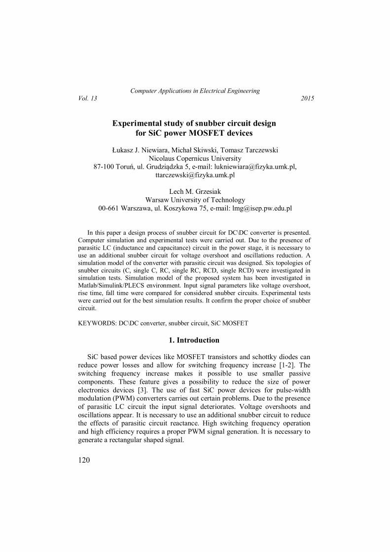
This paper considers three types of snubber circuits shown in Fig. 3.
Simulation tests of the converter with additional snubber circuits has been investigated in a Matlab/Simulink/PLECS environment. Designed simulation model contain the parasitic inductance and capacitance (Fig. 1). It was necessary to determine the parameters of the parasitic circuit in order to create a proper simulation converter circuit model. The semiconductors output capacitance was measured using APPA 703 LCR METER. Determination of circuit inductance required frequency measurement of the input signal oscillations. The frequency was measured using TEKTRONIX TPS2024B oscilloscope with Tektronix P5122 voltage probe. It was not necessary to take into account frequency changes caused by damping in the circuit. The used approximation does not affect the behavior of proposed circuit model. The inductance can be calculated from resonant frequency of LC circuit as follows:
Cf4
1L 22 (1)
where: L - parasitic inductance, f – input signal oscillations frequency, C – parasitic capacitance. Experimentally determined parameters are given in Table 1.
Table 1. Parasitic circuit parameters
Parameter Value Unit Parameter Value Unit Parameter Value Unit
C 1.7 nF f 9.63 MHz L 158.4 nH
Ł. J. Niewiara, M. Skiwski, T. Tarczewski, L. M. Grzesiak / Experimental study ...
123
Fig. 3. Snubber configuration: a) additional capacitor, b) RC snubber, c) RCD snubber, d) additional single capacitor, e) RC snuber – single, f) RCD snubber – single
4. Simulation test results
The behavior of PWM input signal, obtained in a simulation study
environment for converter with additional capacitor (Fig. 3a) is shown in Fig. 4. It can be seen that the use of capacitors for the snubber circuit reduces the voltage overshoot and oscillations (with comparison to waveform presented in Fig. 2). The overshoot value is still significant and is about 60 V. Relative long fall time observed in Fig. 4 is caused by capacitor discharging. Large overshoot and long fall time cause, that considered snubber configuration is not suitable for high frequency DC/DC converter.
The behavior of input signal obtained in a simulation study environment for circuit with RC snubber circuit (Fig. 3b) is shown in Fig. 5. It can be seen that the use of an additional RC circuit reduces the voltage overshoot and oscillations. The overshoot value is about 40 V. There also can be seen the increase of fall time but it is smaller with comparison to snubber with single capacitor. The energy stored in the capacitor were dissipated on the resistor. The presence of an additional resistor improves energy losses in a converter. Considered snubber topology cannot be used in a high efficiency converter.
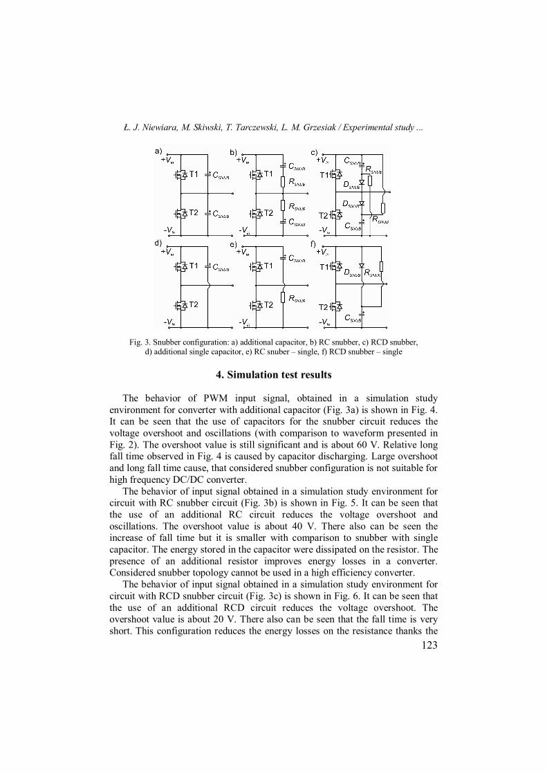
The behavior of input signal obtained in a simulation study environment for circuit with RCD snubber circuit (Fig. 3c) is shown in Fig. 6. It can be seen that the use of an additional RCD circuit reduces the voltage overshoot. The overshoot value is about 20 V. There also can be seen that the fall time is very short. This configuration reduces the energy losses on the resistance thanks the

Ł. J. Niewiara, M. Skiwski, T. Tarczewski, L. M. Grzesiak / Experimental study ...
124
diode. Due to small overshoot and fall time, considered snubber topology is suitable for use in a SiC MOSFET based DC/DC converter.
Fig. 4. Input signal with additional capacitors
Fig. 5. Input signal with RC snubber
The behavior of PWM input signal, obtained in a simulation study
environment for converter with additional capacitor (Fig. 3d) is shown in Fig. 7. It can be seen that the use of a capacitor (between +Vin and –Vin rail) for the snubber circuit reduces the voltage overshoot and oscillations. The overshoot value is also reduced and is about 16V. The fall time is about 105 ns. Some voltage oscillations can be seen. Due to small overshoot and fall time, considered snubber topology is suitable for use with SiC MOSFET.
Ł. J. Niewiara, M. Skiwski, T. Tarczewski, L. M. Grzesiak / Experimental study ...
125
Fig. 6. Input signal with RCD snubber
Fig. 7. Input signal with additional single capacitor
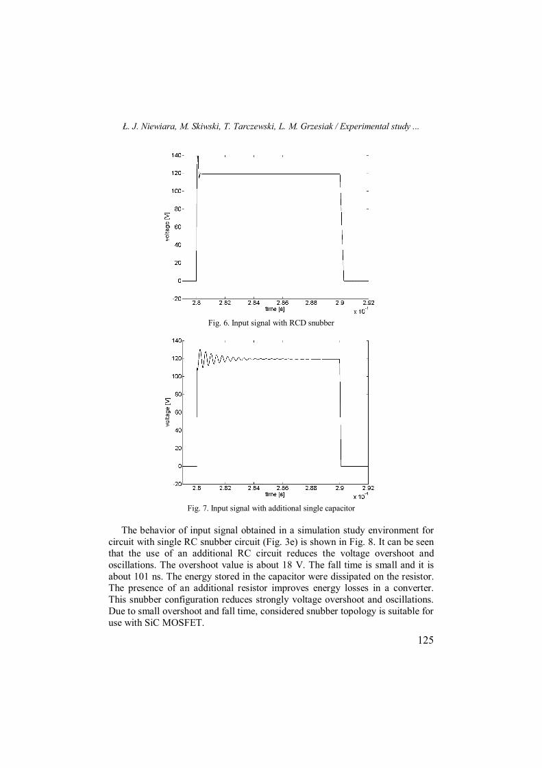
The behavior of input signal obtained in a simulation study environment for
circuit with single RC snubber circuit (Fig. 3e) is shown in Fig. 8. It can be seen that the use of an additional RC circuit reduces the voltage overshoot and oscillations. The overshoot value is about 18 V. The fall time is small and it is about 101 ns. The energy stored in the capacitor were dissipated on the resistor. The presence of an additional resistor improves energy losses in a converter. This snubber configuration reduces strongly voltage overshoot and oscillations. Due to small overshoot and fall time, considered snubber topology is suitable for use with SiC MOSFET.

Ł. J. Niewiara, M. Skiwski, T. Tarczewski, L. M. Grzesiak / Experimental study ...
126
Fig. 8. Input signal with single RC snubber
The behavior of input signal obtained in a simulation study environment for
circuit with single RCD snubber circuit (Fig. 3f) is shown in Fig. 9. It can be seen that the use of an additional RCD circuit reduces the voltage overshoot. The overshoot value is about 14 V. There also can be seen that the fall time is very short. This configuration reduces the energy losses on the resistance thanks the diode. Due to small overshoot and fall time, considered snubber topology is suitable for use in a SiC MOSFET based DC/DC converter.
Table 2. contains input signal quality indicators for different snubber configurations. It can be seen that the last four configurations have very good parameters for almost all indicators. Voltage overshoot is given by following equation:
%100V
VVV
ininmax
O
(2)
where: VO – voltage overshoot, Vmax – maximum input voltage value, Vin – input voltage.
The rise time refers to the time taken by input signal to change from 10% of nominal value to 90% of nominal value. Fall time refers to the time taken by input signal to change from 90% of nominal value to 10% of nominal value respectively. They are given by:
%10r%90rr ttt (3)
%90f%10ff ttt (4) where: tr – rise time, tr10% - time for 10% of input voltage value on rising edge, tr90% - time for 90% of input voltage value on rising edge, tf – fall time, tf10% -

Ł. J. Niewiara, M. Skiwski, T. Tarczewski, L. M. Grzesiak / Experimental study ...
127
time for 10% of input voltage value on falling edge, tf90% - time for 90% of input voltage value on falling edge.
Ts2% refers to the time after which the signal reaches the ±2% path of the nominal value. From simulation results it can be seen that four snubber configurations are suitable for use in high switching frequency applications.
Table 2. Input signal quality indicators for different snubber configurations
Configuration VO [%] tr [µs] tf [µs] Ts2% [µs] - 111.00 0.042 0.207 4.522 C 49.53 0.266 6.831 4.430
RC 28.13 0.033 1.167 0.149 RCD 16.35 0.025 0.218 0.229
C single 13.33 0.020 0.105 2.762 RC single 15.00 0.021 0.101 0.135
RCD single 10.71 0.020 0.110 0.213
Fig. 9. Input signal with single RCD snubber
5. Experimental test results
Experimental tests were obtained for DC\DC converter (Fig. 10). As a power
devices SiC MOSFET transistors (C2M0080120D) [7] and SiC shottky diodes (C4D10120A) [8] were used. PWM input signal was measured using TEKTRONIX TPS2024B oscilloscope with Tektronix P5122 voltage probe. The

Ł. J. Niewiara, M. Skiwski, T. Tarczewski, L. M. Grzesiak / Experimental study ...
128
switching frequency was set to 50 kHz. To generate PWM signal dSpace DS1104 R&D controller board was used.
Fig. 10. DC/DC converter Based on simulation results snubber topologies with the best properties were
chosen for experimental tests. In all cases voltage overshoot doesn’t exceed 20V. The use of snubber improves the quality of the input signal. Fig. 11 contains single PWM signals for different snubber circuits. Proper operation of power transistors, in this case SiC MOSFETS, could not be realized without snubbers (Fig. 11a). The use of some snubber types allows to improve input signal shape and quality (Fig. 11b-e).
Snubber circuit parameters are shown in Table 3. All components should have a low inductance value, to reduce voltage spikes. For this reason it was necessary to use foil capacitors and low inductance resistors (metal oxide film resistor). It was necessary to use a fast diode with low charge for RCD snubbers. Silicon Carbide based shottky diodes were used.
Table 3. Snubber circuit parameters
Configuration C [nF] R [Ω] Diode QC [nC] - - - -
RCD 22.0 10.0 10.0 C single 22.0 - -
RC single 22.0 10.0 - RCD single 22.0 10.0 10.0

Ł. J. Niewiara, M. Skiwski, T. Tarczewski, L. M. Grzesiak / Experimental study ...
129
Fig. 11. Single PWM signals for: a) no snubber, b) RCD snubber, c) single C snubber,
d) single RC snubber, e) single RCD snubber
Quality indicators were calculated for investigated PWM input signals. Following indicators were chosen: voltage overshoot (2), rise time (3) and fall time (4). Table 4 contains calculated values of them.
It can be seen that experimental results are similar to simulation results. The differences can be caused by: simplified simulation model of the investigated circuits (parasitic parameters of passive components for snubbers weren’t taken into account), parameters inaccuracy of used passive components and presence of measurement noise in experimental tests.
Ł. J. Niewiara, M. Skiwski, T. Tarczewski, L. M. Grzesiak / Experimental study ...
130
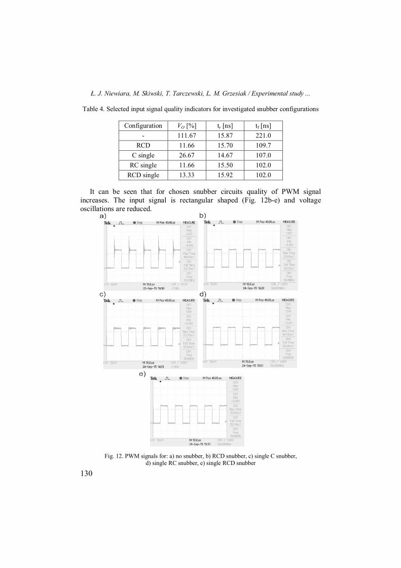
Table 4. Selected input signal quality indicators for investigated snubber configurations
Configuration VO [%] tr [ns] tf [ns] - 111.67 15.87 221.0
RCD 11.66 15.70 109.7 C single 26.67 14.67 107.0
RC single 11.66 15.50 102.0 RCD single 13.33 15.92 102.0
It can be seen that for chosen snubber circuits quality of PWM signal
increases. The input signal is rectangular shaped (Fig. 12b-e) and voltage oscillations are reduced.
Fig. 12. PWM signals for: a) no snubber, b) RCD snubber, c) single C snubber,
d) single RC snubber, e) single RCD snubber

Ł. J. Niewiara, M. Skiwski, T. Tarczewski, L. M. Grzesiak / Experimental study ...
131
6. Conclusion
It was found that using of snubber circuit improves the input signal shape, reduces voltage overshoots and oscillations. Simulation tests show that single C, both RC and both RCD snubber circuits reduces input signal oscillations. However double RC configuration has a longer fall time and dissipates more energy in every cycle than the other configurations. The use of double capacitor based snubber does not produce the correct rectangular shape of the input signal. Because of this it is not suitable for this application.
Experimental tests confirm that single C and single RC snubbers reduces voltage oscillations and voltage overshoot. Also for RCD snubbers similar features were observed.
Some voltage oscillations can be seen in steady state for single C configuration. Additional resistor (single RC configuration) eliminates steady state oscillations, but it may increase energy losses. The use of diode in snubber circuit (RCD) reduces energy losses for turn on operation. Four snubber circuits, single C, single RC, and both RDC, are suitable for high switching frequency devices.
References
[1] Zdanowski M., Rąbkowski J., Barlik R., Transformers. High frequency DC/DC
converter with Silicon Carbide devices - simulation analysis, Przegląd Elektrotechniczny, nr 2/2014, 2014, p. 201-204 (in Polish).
[2] Singh R.., Richmond J., SiC power schottky diodes in power –factor correction circuits, CREE inc. www.cree.com/power.
[3] Niewiara L. J., Tarczewski T., Skiwski M., Grzesiak L. M., 9kW SiC MOSFET based DC/DC converter, Procedings of 17th European Conference on Power Electronics and Applications EPE’15 ECCE Europe, 2015, P.1 – P.9.
[4] Peng F.Z., Su G-J., Tolbert L.M., A passive soft-switching Snubber for PWM inverters, IEEE Transactions on Power Electronics, Volume 19, Number 2, 2004, p. 363-370.
[5] Jain P.K., Kang W., Soin H., Xi Y., Analysis and design considerations of a load and line independent zero voltage switching full bridge DC/DC converter topology, IEEE Transactions on Power Electronics, Volume 17, Number 5, 2002, p. 649-657.
[6] Todd P.C., Snubber circuits: theory, design and applications, Unitrode-Power Supply Design Seminar, 1993.
[7] C2M0080120D SiC N-channel MOSFET datasheet, Rev. B, www.cree.com [8] C4D10120A SiC schottky diode datasheet, Rev. B, www.cree.com (Received: 30. 09. 2015, revised: 7. 12. 2015)