Experimental disclosing the composition- and structure ...
21
Experimental disclosing the composition- and 1 structure-dependent deep-level defect in photovoltaic 2 antimony trisulfide materials 3 4 Weitao Lian 1 Chenhui Jiang 1 , Yiwei Yin 1 , Rongfeng Tang 1 , Gang Li 1 , Lijian 5 Zhang 1 , Bo Che 1 and Tao Chen 1 * 6 7 1 Hefei National Laboratory for Physical Sciences at Microscale, CAS Key 8 Laboratory of Materials for Energy Conversion, Department of Materials Science 9 and Engineering, School of Chemistry and Materials Science, University of Science 10 and Technology of China, Hefei, Anhui 230026, P. R. China 11 12 *E-mail: [email protected] 13 14 15 16 17 18 19 20 21 22
Transcript of Experimental disclosing the composition- and structure ...

Experimental disclosing the composition- and 1
structure-dependent deep-level defect in photovoltaic 2
antimony trisulfide materials 3
4
Weitao Lian1 Chenhui Jiang1, Yiwei Yin1, Rongfeng Tang1, Gang Li1, Lijian 5
Zhang1, Bo Che1 and Tao Chen1* 6
7
1Hefei National Laboratory for Physical Sciences at Microscale, CAS Key 8
Laboratory of Materials for Energy Conversion, Department of Materials Science 9
and Engineering, School of Chemistry and Materials Science, University of Science 10
and Technology of China, Hefei, Anhui 230026, P. R. China 11
12
*E-mail: [email protected] 13
14
15
16
17
18
19
20
21
22

Antimony trisulfide (Sb2S3) represents a kind of emerging light-harvesting material 23
with excellent stability and abundant elemental storage. Due to the low-symmetry, 24
theoretical investigation has pointed out that there exists complicated defect properties. 25
However, there is no experimental verification on the defect property. Here, we conduct 26
optical deep-level transient spectroscopy to investigate defect properties in Sb2S3 and 27
show that there are maximum three kinds of deep level defects observed, depending on 28
the composition of Sb2S3. We also find that the Sb-interstitial (Sbi) defect does not show 29
critical influence on the carrier lifetime, indicating the high tolerance of the one-30
dimensional crystal structure where the space of (Sb4S6)n ribbons is able to 31
accommodate impurities to certain extent. This work provides basic understanding on 32
the defect properties of quasi-one-dimensional materials and a guidance for the 33
efficiency improvement of Sb2S3 solar cells.34

1
Point defect engineering of semiconducting materials is essential for photovoltaic 35
devices, comprehensive understanding of the defects formation mechanism and 36
function enables achieving high-efficiency solar energy conversion. In specific, the 37
point defect (intrinsic or extrinsic defect) determines the Fermi level (EF), free carrier 38
concentration and conductivity type (n or p) of semiconductors. Shallow-level defects 39
with thermal energy of about kBT (where kB is Boltzmann constant, T is temperature) 40
from conduction band minimum (CBM) or valence band maximum (VBM) plays the 41
major role to tune the carrier concentrations and conductivity type. In contrast, deep-42
level defects whose activation energy is much higher than kBT from CBM or VBM is 43
detrimental to photogenerated carrier lifetime and transport (carrier mobility and 44
diffusion length).1 This defect results in the trap-assisted Shockley-Read-Hall (SRH) 45
recombination2, 3 (dominant non-radiation recombination) in solar cells, which is the 46
primary cause of open-circuit voltage (VOC) loss. 47
Recently, binary antimony chalcogenides Sb2S(e)3 (including Sb2S3, Sb2Se3, 48
Sb2(S,Se)3) have drawn increasing attention in solar cell applications, for their large 49
visible light absorption coefficient (> 105 cm-1), earth-abundant compositional elements 50
and tunable band gap in 1.1-1.7 eV. The efficiency breakthrough towards 10% in alloy-51
type antimony selenosulfide stimulating new interests in the development of this class 52
of materials4, 5. In particular, Sb2S3 with band gap of ~1.7 eV can be perfectly applied 53
as top cell material for the construction of tandem solar cells. Different from previous 54
photovoltaic materials such as silicon, Cu(In, Ga)Se2, CdTe and organic-inorganic 55
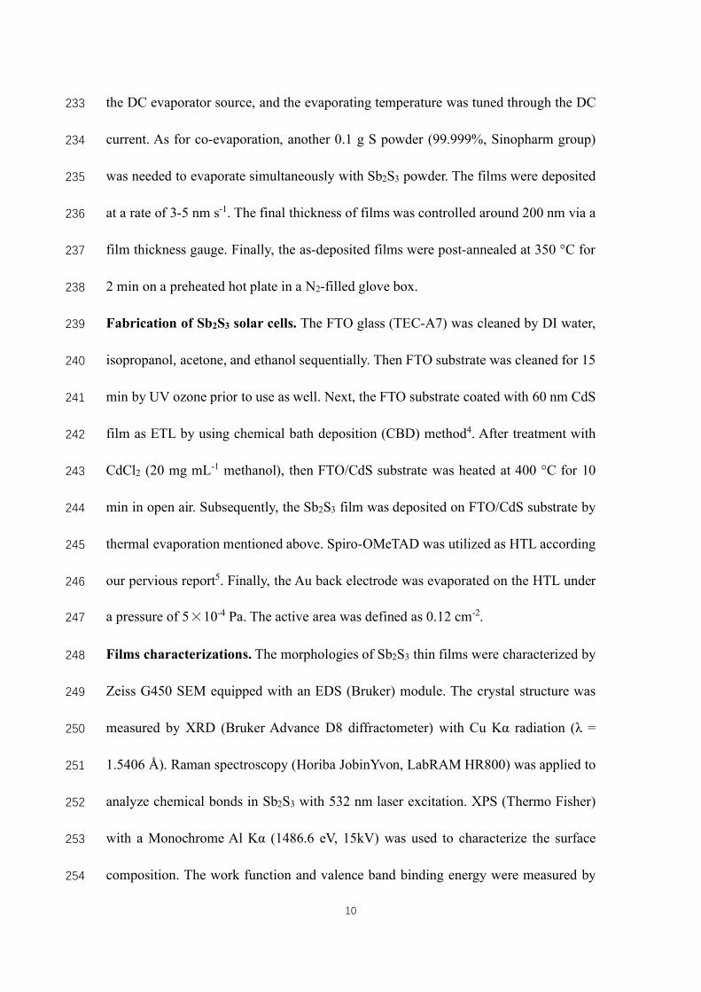
hybrid perovskite, the Sb2S3 displays quasi-one-dimensional structure composed of 56

2
[Sb4S6]n ribbons and could generate benign grain boundaries without dangling bonds 57
along c axis (Fig. 1)6, 7. In practical, to transfer the distinctive structural advantage into 58
efficient carrier transport and final power conversion efficiency (PCE), one must 59
understand and control the defect properties, in particular the deep-level defects. This 60
requirement has spurred intense interests in exploring the defect properties of such 61
materials, especially from theoretical perspective, which revealed complicated defect 62
characteristics although it has only two kinds of elements8-11. However, to date there is 63
a lack of experimental verification of defect properties associated with the structure and 64
compositions, which induces ambiguity in the fabrication of high quality Sb2S3 films 65
for efficient solar cells. 66
Herein, we experimentally uncover the defect characteristics by using deep level 67
transient spectroscopy (DLTS) and identify the details of the defect. We examine both 68
Sb-rich and S-rich Sb2S3 films for a comparative study which is prepared by thermal 69
evaporation approach. To make clear conclusions, we carefully analyze the crystallinity, 70
electronic structure and chemical composition (impurity) of the as-obtained films. In 71
contrast to the theoretical study where complicated defect proposed in the Sb2S38-11, our 72
experimental investigation shows only a few types of defect, and the defect type and 73
concentration is sensitively dependent on anion/cation ratio. 74
Results 75
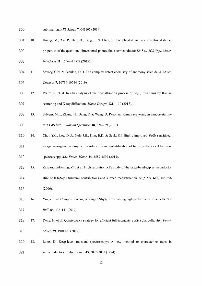
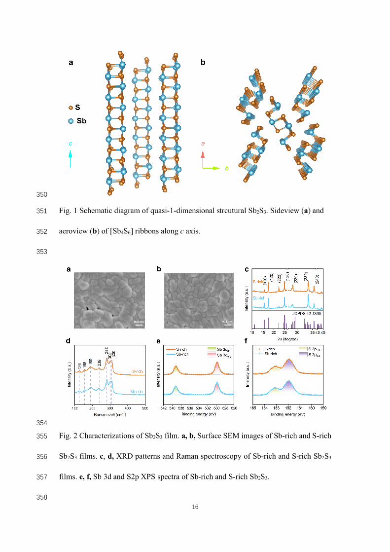
Structure and composition characterization of Sb2S3 films. Due to the high saturated 76
vapor pressure of sulfur, the sulfur loss is inevitable and results in Sb-rich films during 77
thermal evaporation deposition. To obtain S-rich Sb2S3 film, we apply a co-evaporation 78

3
equipment for the Sb2S3 film fabrication, in which S powders are co-evaporated with 79
Sb2S3 for the generation S-rich Sb2S3 films. The synthesis details are provided in the 80
Methods section. The as-obtained films at Sb-rich and S-rich conditions display similar 81
morphology (Fig. 2a, 2b and Supplementary Fig. 1). X-ray diffraction (XRD) is then 82
applied to characterize the crystallinity (Fig. 2c). Both of the films display diffractions 83
at 15.6, 17.5, 24.9, 33.6 and 35.6 °, which are well assigned as (020), (120), (130), 84
(330) and (240) crystal planes of orthorhombic Sb2S3 (JCPDS No. 42-1393, Pbnm)6. 85
According to the energy dispersive X-ray spectroscopy (EDS), the atomic ratio of S/Sb 86
in Sb-rich and S-rich Sb2S3 films are calculated to be 1.28 to 1.55 (Supplementary Table 87
1), respectively. 88
Impurity crucially influences the defect properties in a semiconductor. In this case, 89
we carry out Raman scattering and X-ray photoelectron spectroscopy (XPS) 90
characterizations to carefully examine the bulk and surface chemical compositions. 91
Raman spectra show typical antisymmetric and symmetric bending vibration of S-Sb-92
S at 189 and 239 cm-1 (Fig. 2d), respectively. The antisymmetric and symmetric 93
stretching vibration of Sb-S appear at 282 and 309 cm-1. Furthermore, Raman shift at 94
126 and 156 cm-1 correspond to crystalline Sb2S3 phase12. In addition, Raman scattering 95
at 302 cm-1 is ascribed to the phonon scattering from CdS substrate13. 96
XPS spectra (Fig. 2e and f) display typical binding energy of 539.2 eV and 529.8 eV 97
which are assigned to Sb 3d3/2 and 3d5/2 of Sb2S3, respectively. Notably, there is no 98
existence of SbOx in both films, which is commonly generated as impurity in the 99
synthesis of Sb2S3 and displays deep defects characteristics14. In addition, the binding 100

4
energy of 163.1 eV and 161.9 eV are ascribed to the S 2p1/2 and 2p3/2 of Sb2S36, 14, 15. 101
From both Raman scattering and XPS analysis, both Sb-rich and S-rich Sb2S3 films 102
prepared via thermal evaporation are free of impurities, which thus provides excellent 103
platform for the investigations of the defect properties. 104
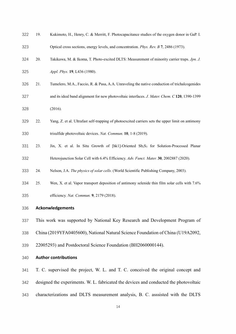
Photovoltaic performance of devices. To test the optoelectronic quality of the as-105
synthesized film at device level, we examine the solar cell efficiency by using CdS and 106
Spiro-OMeTAD as electron and hole transport layer (ETL & HTL), respectively (Fig. 107
3a and b). The current density-voltage (J-V) curves are obtained under standard AM 108
1.5G illumination (Fig. 3c). The optimal Sb-rich Sb2S3 based solar cell delivers PCE of 109
5.0%, with open-circuit voltage (VOC), short-circuit current density (JSC) and fill factor 110
(FF) of 0.68 V, 15.4 mA cm−2 and 47.6%, respectively. While the optimal S-rich Sb2S3 111
device generate a PCE of 6.2% (VOC of 0.72 V, JSC of 15.9 mA cm−2 and FF 54.3%) 112
with a net increase by 1.2% than the Sb-rich Sb2S3 based device. This PCE represents 113
the highest value in thermal evaporation derived Sb2S3 solar cells16, 17. The statistic 114
parameters (VOC, JSC, FF, and PCE) of each type of devices show narrow distributions 115
(Supplementary Fig. 2a-e), confirming the reliability of the film and device fabrication. 116
Moreover, the external quantum efficiency (EQE) spectra (Fig. 3d and Supplementary 117
Fig. 2f) display excellent photocurrent generation efficiency in the 500-700 nm, a 118
decrease in the short wavelength is attributed to the light absorption loss induced by 119
CdS since its band gap is 2.4 eV. On the ground of both J-V and EQE analysis, the as-120
prepared S-rich Sb2S3 films display high photovoltaic quality. 121
Bulk deep-level defects analysis. In this characterization, there is a typical concern on 122
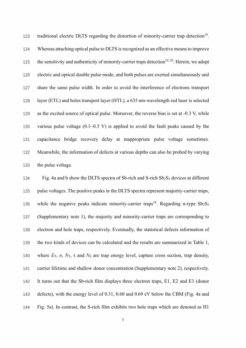
5
traditional electric DLTS regarding the distortion of minority-carrier trap detection18. 123
Whereas attaching optical pulse to DLTS is recognized as an effective means to improve 124
the sensitivity and authenticity of minority-carrier traps detection19, 20. Herein, we adopt 125
electric and optical double pulse mode, and both pulses are exerted simultaneously and 126
share the same pulse width. In order to avoid the interference of electrons transport 127
layer (ETL) and holes transport layer (HTL), a 635 nm-wavelength red laser is selected 128
as the excited source of optical pulse. Moreover, the reverse bias is set at -0.3 V, while 129
various pulse voltage (0.1~0.5 V) is applied to avoid the fault peaks caused by the 130
capacitance bridge recovery delay at inappropriate pulse voltage sometimes. 131
Meanwhile, the information of defects at various depths can also be probed by varying 132
the pulse voltage. 133
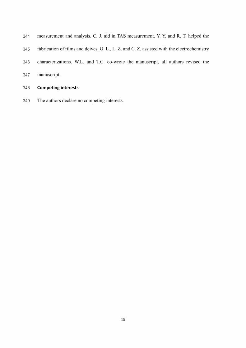
Fig. 4a and b show the DLTS spectra of Sb-rich and S-rich Sb2S3 devices at different 134
pulse voltages. The positive peaks in the DLTS spectra represent majority-carrier traps, 135
while the negative peaks indicate minority-carrier traps18. Regarding n-type Sb2S3 136
(Supplementary note 1), the majority and minority-carrier traps are corresponding to 137
electron and hole traps, respectively. Eventually, the statistical defects information of 138
the two kinds of devices can be calculated and the results are summarized in Table 1, 139
where ET, σ, NT, τ and NS are trap energy level, capture cross section, trap density, 140
carrier lifetime and shallow donor concentration (Supplementary note 2), respectively. 141
It turns out that the Sb-rich film displays three electron traps, E1, E2 and E3 (donor 142
defects), with the energy level of 0.31, 0.60 and 0.69 eV below the CBM (Fig. 4a and 143
Fig. 5a). In contrast, the S-rich film exhibits two hole traps which are denoted as H1 144

6
and H2 (acceptor defects) with energy levels of 0.64 and 0.71 eV above the VBM (Fig. 145
4b and Fig. 5b). In comparison to the calculations on the defect energy levels8, 9, 21, the 146
traps E1, E2 and E3 are well assigned to Sb-interstitial (Sbi), S-vacancy (VS), and 147
antisite of Sb for S (SbS) defects, respectively. The traps H1 and H2 in S-rich Sb2S3 are 148
ascribed to Sb-vacancy (VSb) and antisite of S for Sb (SSb), respectively. This 149
characterization suggests clearly the composition-depended defect properties of Sb2S3 150
films. 151
Notably, according the energy level alignment (Fig. 5a and b), these are all deep-152
level defects whose energy level are more than 0.3 eV far from CBM or VBM. 153
Therefore, they are supposed to act as carrier traps or recombination sites due to their 154
high ionization energy. Specially, the trap E2, E3, H1 and H2 possess deeper energy 155
level (close to intrinsic EF), large capture cross section and high trap density (Table 1) 156
which accord with basic characteristics of SRH recombination centers. Thus, they 157
behave seriously as recombination centers to hinder carrier transport and shorten the 158
carrier lifetime. 159
Carrier dynamic analysis. To study the charge transport kinetics, we perform transient 160
absorption spectroscopy (TAS) measurement of the Sb-rich and S-rich Sb2S3 films 161
deposited on soda-lime glass. We apply glass/Sb2S3 films without any electron or hole 162
extraction layer as sample for this study, which can reflect unambiguously that the 163
exciton relaxes to ground state through charge recombination in films. The TAS is 164
tracked at a time window of 5 -5000 ps using 400 nm pulse laser excitation for Sb-rich 165
and S-rich Sb2S3 films (Fig. 6a and b, Supplementary Fig. 5). Strikingly, there appear 166

7
two photo-induced absorption peaks near 545 and 690 nm, both of which are assigned 167
to a single broad feature of trapped carrier in Sb2S3. Especially, the peak at 690 nm is 168
associated with the formation of sulfide radical22, 23. Thus, the enhanced absorption at 169
690 nm for S-rich Sb2S3 could be attributed to abundant sulfide radical. Accordingly, 170
the decay characteristics at 545 nm are fitted by biexponential model to study carrier 171
decay kinetics (Fig. 6c and Supplementary Table 2). It is observed that the S-rich Sb2S3 172
exhibits much longer carrier lifetime (18.7 ns) than Sb-rich Sb2S3 (3.8 ns), the reduced 173
defect type and concentration contribute the prolonged lifetime. 174
To gain further insight into the specific influence of each defect on the carrier 175
dynamics, we extract the limited carrier lifetime associated with specific defect by trap-176
assisted SRH recombination according to equation 1. 177
� = (������)��. (1) 178
where the υth is thermal velocity for electron (hole) that is about 107 cm/s in bulk 179
semiconductors at room temperature2, 3, 24. Both σ and NT can be obtained from DLTS. 180
Consequently, the defect with large capture cross section, high trap density and deep 181
trap energy level are much more detrimental to carrier lifetime. 182
In Sb-rich Sb2S3 film, the carrier lifetime is limited by trap E2 (VS) and E3 (SbS) in 183
Sb-rich Sb2S3 film which are estimated to be 64.6 and 28.4 ns (Table 1), respectively. 184
The other defect E1 (Sbi) present carrier lifetime of 2180 ns, much longer than those of 185
E2 and E3. This result should be associated with the crystal structure where the Sb 186
atoms enters into the space between (Sb4S6)n ribbons is less detrimental to the carrier 187
transport dynamics. In S-rich Sb2S3 film, the trap H1 (VSb) sets the limited lifetime of 188

8
48.3 ns, while the lifetime limited by trap H2 (SSb) is 997 ns. Defect SSb shows less 189
detriment to carrier lifetime since the low concentration due to high formation energy9, 190
even though it manifests deeper energy level than VSb. 191
In the first sense, we compare the shortest carrier lifetime limited by E3 and H1, we 192
suppose that this prolonged carrier lifetime is attributed to reduced capture cross section 193
and trap density of H1. In fact, the recombination form in real semiconductors is mostly 194
multi-level recombination24. That is to say, the carriers leap among multiple trap level 195
and get recombination ultimately. Therefore, the decreased defect numbers in S-rich 196
Sb2S3 also contribute the longer carrier lifetime. It is worthy of noting that the calculated 197
carrier lifetime estimated based on bulk trap-assisted SRH recombination model should 198
be slightly exaggerated since it does not consider other non-radiation recombination 199
such as Auger recombination and interface recombination. In any case, the carrier 200
lifetime calculated by bulk trap-assisted SRH recombination model shows the similar 201
trend at the same scale when compared with that obtained by TAS, suggesting that it is 202
the intrinsic deep-level defects that restrict the carrier lifetime in Sb2S3. 203
Discussion 204
For the Sb2S3 solar cell development, one of the major concern is the efficiency 205
improvement. The rational engineering of the defect properties benefits the carrier 206
transport and suppress the negative recombination, which further improve three device 207
parameters, VOC, JSC and FF. In particular, it has been acknowledged that there is a 208
serious VOC loss in the Sb2S3 solar cell. Fundamentally, the VOC of solar cell originates 209
from the split of quasi-Fermi level for electron and hole (Fig. 5c)24, 25. The trap E2 and 210

9
E3 in Sb-rich Sb2S3 films with large capture cross section and high trap density, 211
especially trap energy level closer to Fermi level compared with H1 and H2 in S-rich 212
Sb2S3. There is high possibility that the electron quasi-Fermi level is pinned near trap 213
E2 and E3 in Sb-rich Sb2S3 owing to inefficient extraction of trapped photo-exited 214
carriers. In contrast, S-rich Sb2S3 displays decrescent capture cross section, defects 215
density and defects numbers which jointly give rise to suppressive recombination and 216
prolonged carrier lifetime. This characteristic is able to alleviate the Fermi level pinning 217
effects and improving VOC ultimately. 218
An interesting finding in this study is that the existence of Sbi in the Sb-rich Sb2S3 219
film generates less detrimental effect on the carrier lifetime, which should be related to 220
Q1D crystal structure where the space between (Sb4S6)n ribbons can afford impurities 221
to certain degree. However, the Si defect does not appear in the S-rich Sb2S3 film, it is 222
most likely that the sulfur is easy to be evaporate out during the film deposition at high 223
temperature. Finally, we find that the Sb-rich film displays two types of crucial defect, 224
i.e. VS and SbS, while S-rich Sb2S3 film shows only one kind of critical defect, VSb. 225
Therefore, the S-rich Sb2S3 film seems more promising for achieving next efficiency 226
breakthrough, provided that the VSb is well suppressed without introducing other deep-227
level defects. 228
Methods 229
Preparation of Sb2S3 thin films. The Sb2S3 films were deposited on FTO/CdS 230
substrate preheated at 300 °C via thermal evaporation under pressure of 0.2~0.3 Pa. 231
About 0.3 g Sb2S3 powder (99.9%, aladdin) was put into a tungsten boat equipped on 232
10
the DC evaporator source, and the evaporating temperature was tuned through the DC 233
current. As for co-evaporation, another 0.1 g S powder (99.999%, Sinopharm group) 234
was needed to evaporate simultaneously with Sb2S3 powder. The films were deposited 235
at a rate of 3-5 nm s-1. The final thickness of films was controlled around 200 nm via a 236
film thickness gauge. Finally, the as-deposited films were post-annealed at 350 °C for 237
2 min on a preheated hot plate in a N2-filled glove box. 238
Fabrication of Sb2S3 solar cells. The FTO glass (TEC-A7) was cleaned by DI water, 239
isopropanol, acetone, and ethanol sequentially. Then FTO substrate was cleaned for 15 240
min by UV ozone prior to use as well. Next, the FTO substrate coated with 60 nm CdS 241
film as ETL by using chemical bath deposition (CBD) method4. After treatment with 242
CdCl2 (20 mg mL-1 methanol), then FTO/CdS substrate was heated at 400 °C for 10 243
min in open air. Subsequently, the Sb2S3 film was deposited on FTO/CdS substrate by 244
thermal evaporation mentioned above. Spiro-OMeTAD was utilized as HTL according 245
our pervious report5. Finally, the Au back electrode was evaporated on the HTL under 246
a pressure of 5×10⁻⁴ Pa. The active area was defined as 0.12 cm-2. 247
Films characterizations. The morphologies of Sb2S3 thin films were characterized by 248
Zeiss G450 SEM equipped with an EDS (Bruker) module. The crystal structure was 249
measured by XRD (Bruker Advance D8 diffractometer) with Cu Kα radiation (λ = 250
1.5406 Å). Raman spectroscopy (Horiba JobinYvon, LabRAM HR800) was applied to 251
analyze chemical bonds in Sb2S3 with 532 nm laser excitation. XPS (Thermo Fisher) 252
with a Monochrome Al Kα (1486.6 eV, 15kV) was used to characterize the surface 253
composition. The work function and valence band binding energy were measured by 254

11
UPS (Thermo Escalab 250Xi, He I excitation 21.22 eV) which were recorded at 0 V 255
samples bias in an ultrahigh vacuum chamber. TAS of Sb2S3 films were measured by a 256
Helios setup, where a nondegenerate pump–probe configuration was applied to probe 257
the transient dynamics (50 fs to 7 ns). Additionally, the pump and probe laser pulses 258
were generated by frequency doubling the fundamental output (Coherent Vitesse, 80 259
MHz, Ti-sapphire laser) and white light generated with a sapphire plate, respectively. 260
The decay characteristics were fitted by biexponential model y=ΣAiexp(-x/ti), while 261
carrier lifetime (τ) was obtained by τ=ΣAiti2/ΣAiti (i=2). 262
Devices characterizations. The J-V characteristics were performed by Keithley 2400 263
apparatus under solar-simulated AM 1.5 sunlight (100 mW cm-2) with a standard xenon-264
lamp-based solar simulator (Oriel Sol 3A, Japan). Prior to test, the solar simulator 265
illumination intensity was calibrated by a monocrystalline silicon reference cell (Oriel 266
P/N 91150 V, with KG-5 visible color filter) which is also calibrated by the National 267
Renewable Energy Laboratory (NREL). The EQE (model SPIEQ200) was measured 268
using a single-source illumination system (halogen lamp) combined with a 269
monochromator. The DLTS measurement was performed via a Phystech FT-1230 270
HERA-DLTS system equipped with a 10 mW laser of 635 nm wavelength. And the 271
optical pulse was generated from the laser. The modified Boonton 7200 capacitance 272
meter (high frequency, 1 MHz) was used to observe capacitance dynamically. The 273
samples were placed in a liquid-helium cryostat (Lakeshore 335,336). The DLTS 274
temperature scan range varies from 120 to 420 K at 2 K intervals. The pulse mode was 275
set as electrical (fill voltage) and optical (laser excitation) pulse yielding simultaneously. 276

12
In detail, the reverse bias, pulse voltage, pulse width (electric & optical), and period 277
width were −0.3 V, 0.1~0.5 V, 10 ms and 100 ms, respectively. 278
Data avilible 279
All data that support the findings of this study are available within the paper and the 280
supplementary information. 281
Refernces 282
1. Park, J.S., Kim, S., Xie, Z. & Walsh, A. Point defect engineering in thin-film solar cells. Nat. 283
Rev. Mater. 3, 194-210 (2018). 284
2. Hall, R.N. Electron-hole recombination in germanium. Phys. Rev. 87, 387 (1952). 285
3. Shockley, W. & Read Jr, W. Statistics of the recombinations of holes and electrons. Phys. Rev. 286
87, 835 (1952). 287
4. Tang, R. et al. Hydrothermal deposition of antimony selenosulfide thin films enables solar cells 288
with 10% efficiency. Nat. Energy 5, 587-595 (2020). 289
5. Wang, X. et al. Manipulating the Electrical Properties of Sb2(S, Se)3 Film for High‐Efficiency 290
Solar Cell. Adv. Energy Mater. 10, 2002341 (2020). 291
6. Wang, X., Tang, R., Wu, C., Zhu, C. & Chen, T. Development of antimony sulfide–selenide 292
Sb2(S, Se)3-based solar cells. J. Energy Chem. 27, 713-721 (2018). 293
7. Chen, C. & Tang, J. Open-Circuit Voltage Loss of Antimony Chalcogenide Solar Cells: Status, 294
Origin and Possible Solution. ACS Energy Lett. 5, 2294-2304 (2020). 295
8. Cai, Z., Dai, C.-M. & Chen, S. Intrinsic Defect Limit to the Electrical Conductivity and a Two‐296
Step p‐Type Doping Strategy for Overcoming the Efficiency Bottleneck of Sb2S3‐Based Solar 297
Cells. Sol. RRL 4, 1900503 (2020). 298
9. Guo, L. et al. Scalable and efficient Sb2S3 thin-film solar cells fabricated by close space 299
13
sublimation. APL Mater. 7, 041105 (2019). 300
10. Huang, M., Xu, P., Han, D., Tang, J. & Chen, S. Complicated and unconventional defect 301
properties of the quasi-one-dimensional photovoltaic semiconductor Sb2Se3. ACS Appl. Mater. 302
Interfaces 11, 15564-15572 (2019). 303
11. Savory, C.N. & Scanlon, D.O. The complex defect chemistry of antimony selenide. J. Mater. 304
Chem. A 7, 10739-10744 (2019). 305
12. Parize, R. et al. In situ analysis of the crystallization process of Sb2S3 thin films by Raman 306
scattering and X-ray diffraction. Mater. Design. 121, 1-10 (2017). 307
13. Saleem, M.F., Zhang, H., Deng, Y. & Wang, D. Resonant Raman scattering in nanocrystalline 308
thin CdS film. J. Raman Spectrosc. 48, 224-229 (2017). 309
14. Choi, Y.C., Lee, D.U., Noh, J.H., Kim, E.K. & Seok, S.I. Highly improved Sb2S3 sensitized‐310
inorganic–organic heterojunction solar cells and quantification of traps by deep‐level transient 311
spectroscopy. Adv. Funct. Mater. 24, 3587-3592 (2014). 312
15. Zakaznova-Herzog, V.P. et al. High resolution XPS study of the large-band-gap semiconductor 313
stibnite (Sb2S3): Structural contributions and surface reconstruction. Surf. Sci. 600, 348-356 314
(2006). 315
16. Yin, Y. et al. Composition engineering of Sb2S3 film enabling high performance solar cells. Sci. 316
Bull. 64, 136-141 (2019). 317
17. Deng, H. et al. Quasiepitaxy strategy for efficient full‐inorganic Sb2S3 solar cells. Adv. Funct. 318
Mater. 29, 1901720 (2019). 319
18. Lang, D. Deep‐level transient spectroscopy: A new method to characterize traps in 320
semiconductors. J. Appl. Phys. 45, 3023-3032 (1974). 321
14
19. Kukimoto, H., Henry, C. & Merritt, F. Photocapacitance studies of the oxygen donor in GaP. I. 322
Optical cross sections, energy levels, and concentration. Phys. Rev. B 7, 2486 (1973). 323
20. Takikawa, M. & Ikoma, T. Photo-excited DLTS: Measurement of minority carrier traps. Jpn. J. 324
Appl. Phys. 19, L436 (1980). 325
21. Tumelero, M.A., Faccio, R. & Pasa, A.A. Unraveling the native conduction of trichalcogenides 326
and its ideal band alignment for new photovoltaic interfaces. J. Mater. Chem. C 120, 1390-1399 327
(2016). 328
22. Yang, Z. et al. Ultrafast self-trapping of photoexcited carriers sets the upper limit on antimony 329
trisulfide photovoltaic devices. Nat. Commun. 10, 1-8 (2019). 330
23. Jin, X. et al. In Situ Growth of [hk1]‐Oriented Sb2S3 for Solution‐Processed Planar 331
Heterojunction Solar Cell with 6.4% Efficiency. Adv. Funct. Mater. 30, 2002887 (2020). 332
24. Nelson, J.A. The physics of solar cells. (World Scientific Publishing Company, 2003). 333
25. Wen, X. et al. Vapor transport deposition of antimony selenide thin film solar cells with 7.6% 334
efficiency. Nat. Commun. 9, 2179 (2018). 335
Ackonwledgements 336
This work was supported by National Key Research and Development Program of 337
China (2019YFA0405600), National Natural Science Foundation of China (U19A2092, 338
22005293) and Postdoctoral Science Foundation (BH2060000144). 339
Author contributions 340
T. C. supervised the project, W. L. and T. C. conceived the original concept and 341
designed the experiments. W. L. fabricated the devices and conducted the photovoltaic 342
characterizations and DLTS measurement analysis, B. C. asssisted with the DLTS 343
15
measurement and analysis. C. J. aid in TAS measurement. Y. Y. and R. T. helped the 344
fabrication of films and deives. G. L., L. Z. and C. Z. assisted with the electrochemistry 345
characterizations. W.L. and T.C. co-wrote the manuscript, all authors revised the 346
manuscript. 347
Competing interests 348
The authors declare no competing interests. 349
16
350
Fig. 1 Schematic diagram of quasi-1-dimensional strcutural Sb2S3. Sideview (a) and 351
aeroview (b) of [Sb4S6] ribbons along c axis. 352
353
354
Fig. 2 Characterizations of Sb2S3 film. a, b, Surface SEM images of Sb-rich and S-rich 355
Sb2S3 films. c, d, XRD patterns and Raman spectroscopy of Sb-rich and S-rich Sb2S3 356
films. e, f, Sb 3d and S2p XPS spectra of Sb-rich and S-rich Sb2S3. 357
358

17
359
Fig. 3 Device structure and photovoltaic performance. a, b, Cross sectional SEM image 360
and corresponding device configration of Sb2S3 solar cells. c J–V characteristics of the 361
optimal Sb-rich and S-rich Sb2S3 devices under standard one Sun illumination. d EQE 362
spectra of the optimal Sb-rich and S-rich Sb2S3-based devices. 363
364
365
366

18
367
Fig. 4 Deep-level defects characterization. DLTS signals of Sb-rich (a) and S-rich Sb2S3 368
films (b) at pulse voltage ranging from 0.1 to 0.5 V, synergized with an identical pulse-369
width optical pulse. 370
371
372
Fig. 5 Schematic of band structure and heterojunction. a, b, Conduction band (EC), 373
valence band (EV), Fermi level (EF) and trap energy level (ET) for Sb-rich and S-rich 374
Sb2S3 films. c Schematic diagram of VOC derived from heterojunction. 375

19
376
377
Fig. 6 TAS study of Sb2S3 films. a, b, 2D color images of TAS of Sb-rich and S-rich 378
Sb2S3 films. c Transient kinetic decay and fittings (solid lines) monitored at 545 nm of 379
Sb-rich and S-rich films. 380
381
Table 1 Deep-level defect parameters (trap type, trap energy level (ET), capture cross 382
section (σ), trap density (NT), carrier lifetime (τ), shallow donor concentration (NS)) of 383
Sb-rich and S-rich Sb2S3 films. 384
Sample Trap ET (eV) σ (cm2) NT (cm-3) τ (ns) NS (cm-3)
Sb-rich
E1 Ec-0.31±0.02 (0.54~8.13)×10-17 (3.75~5.63)×1014 2.18×10³
7.71×10¹⁶ E2 Ec-0.60±0.02 (0.26~4.68)×10-16 (1.57~3.31)×1015 6.46×101
E3 Ec-0.69±0.02 (0.11~1.75)×10-15 (1.38~2.01)×1015 2.84×101
S-rich
H1 Ev+0.64±0.01 (0.46~1.31)×10-15 (0.45~1.58)×1015 4.83×101
5.13×10¹⁶
H2 Ev+0.71±0.02 (0.49~1.17)×10-16 (6.71~8.57)×1014 9.97×10²
385
386