Exciton-like trap states limit electron mobility in TiO 2 ...
23
Exciton-like trap states limit electron mobility in TiO 2 nanotubes Christiaan Richter † and Charles A. Schmuttenmaer * Nanoparticle films have become a promising low-cost, high- surface-area electrode material for solar cells and solar fuel pro- duction 1,2 . Compared to sintered nanoparticle films, oriented polycrystalline titania nanotubes offer the advantage of directed electron transport, and are expected to have higher electron mobility 3–7 . However, macroscopic measurements have revealed their electron mobility to be as low as that of nanoparticle films 8,9 . Here, we show, through time-resolved terahertz spec- troscopy 10 , that low mobility in polycrystalline TiO 2 nanotubes is not due to scattering from grain boundaries or disorder- induced localization as in other nanomaterials 11,12 , but instead results from a single sharp resonance arising from exciton-like trap states. If the number of these states can be lowered, this could lead to improved electron transport in titania nanotubes and significantly better solar cell performance. Alternative energy sources such as those based on solar power must be developed in order to cut back on greenhouse gas emissions and move away from fossil fuels, and in the last two decades there has been an ever increasing effort to make use of nanomaterials in alternative solar cell designs. One such nanomaterial, discovered in 2001, is composed of ordered titania nanotubes 13 . It has been pro- posed that anodic titania nanotubes may have unique electron transport properties that make them an enabling technology for next-generation solar cells 4,14,15 , including dye-sensitized solar cells (DSSCs) 4–6 , and in photoelectrochemical cells for the production of solar hydrogen 16,17 . Both applications require that free carriers (electrons) be transported through an anodic TiO 2 electrode, either along the length of nanotubes in the case of nanotube electrodes, or through a porous nanoparticle network by means of a random walk in standard DSSCs 2,3,8 . Several authors have suggested that nanotubes would be superior to nanoparticle networks regard- ing the vectorial electron transport required in applications such as DSSCs 5,6,18 . However, whole-cell evaluation of electron mobility through nanotubes has found that they are not much better than nanoparticle films 8 . In this study we use time-resolved terahertz spectroscopy (TRTS) to directly probe and reveal the microscopic electron transport properties of nanotube arrays. We have previously used TRTS to directly probe electron trans- port in TiO 2 nanoparticle films 12 . TRTS revealed that electrons are surprisingly mobile within nanoparticles, but that transport through the nanoparticle film is impeded by the strong backscattering and/or disorder-induced localization of electrons. In other words, electron localization involves the whole particle and thus suggests structural disorder as being the dominant impediment to transport in nanoparticle films. Ordered TiO 2 nanotubes are fabricated by anodizing titanium foil in an electrolyte containing fluoride or chloride, as described in the Methods 4–9,13,15–18 . The halogen anions in the electrolyte disrupt passivation during the electrochemical oxidation of the titanium foil, resulting in the formation of nanotubes (Fig. 1) as the metal foil is transformed into the oxide 15,18 . The as-anodized nanotube films are amorphous and are subsequently transformed into polycrystalline anatase by low-temperature annealing 4–9,13,15–18 . Here, we probe electron injection, cooling and transport in TiO 2 nanotubes on a sub-picosecond timescale using TRTS. We find that, unlike nanoparticles, there is no evidence of significant backscatter- ing or disorder-induced localization. Instead, the conductivity spec- trum of the nanotubes reveals a distinct resonance at 7.5 meV, which corresponds to an exciton-like entity. Hence, even though macroscopic measurements have shown similarly low electron mobilities in TiO 2 nanoparticles when compared to nanotube films, the underlying reasons for this are very different. In previous work we obtained the frequency-dependent complex photoconductivity, ˆ s (v)= s 1 (v)+ is 2 (v), of rutile single crystals and nanoparticle films over terahertz frequencies 12 . As can be seen in Fig. 2 the single crystal demonstrates ideal Drude conductivity. On the other hand, anatase and rutile nanoparticle films of various sizes (7–200 nm) 12,19,20 , as well as ZnO nanoparticle and nanowire films 11 , do not all conform to classical Drude behavior, but instead demonstrate behaviour that can be consistently fit by the extended Drude–Smith model 12,19,21,22 . In all of these samples, the imaginary conductivity, s 2 (v), is negative at low frequencies, corresponding to a Drude–Smith parameter c close to –1, which suggests transport dominated by backscattering and/or disorder- induced localization. A representative ˆ s (v) spectrum for TiO 2 nanotubes is also shown in Fig. 2. In both the nanotube and nanoparticle samples, d.c. conductivity is suppressed, that is, s 1,dc,nano ≪ s 1,dc,crystal , as v 0 (where s 1 is the real part of the complex-valued conduc- tivity), suggesting comparably low electron mobility. However, the nanotube spectrum is fundamentally different from that for single-crystal or nanoparticulate TiO 2 , and is dominated by a sharp resonance at 1.8 THz (7.5 meV). Even though the exper- imental bandwidth extends only up to 1.6 THz when probing the single crystal and nanoparticle samples, it is clear from the lack of downward curvature in s 2 that no oscillator component is present. Furthermore, Tiwana and colleagues recently measured the TiO 2 nanoparticle photoconductivity spectrum to 2.0 THz and did not observe a resonant feature 20 (see Supplementary Information for a detailed discussion). As can be seen in Fig. 3 and the plots in the Supplementary Information, the resonance at 1.8 THz is present in all polycrystal- line nanotube samples, whether annealed at 400 8C or 475 8C, whether stained with N3 (also known as red dye) and photoexcited at 400 nm, or N749 (also known as black dye) and photoexcited at 800 nm. The observed resonance can be fit in all spectra by a single classical Lorentz oscillator (see Supplementary Information for fitting equations and parameter values obtained). Our ˆ s (v) Department of Chemistry, Yale University, 225 Prospect St., New Haven, Connecticut 06520-8107 USA; † Present address: Rochester Institute of Technology, Chemical and Biomedical Engineering, 160 Lomb Memorial Drive, Rochester, New York 14623-5603 USA. *e-mail: [email protected] LETTERS PUBLISHED ONLINE: 17 OCTOBER 2010 | DOI: 10.1038/NNANO.2010.196 NATURE NANOTECHNOLOGY | VOL 5 | NOVEMBER 2010 | www.nature.com/naturenanotechnology 769 © 2010 Macmillan Publishers Limited. All rights reserved.
Transcript of Exciton-like trap states limit electron mobility in TiO 2 ...

Exciton-like trap states limit electron mobilityin TiO2 nanotubesChristiaan Richter† and Charles A. Schmuttenmaer*
Nanoparticle films have become a promising low-cost, high-surface-area electrode material for solar cells and solar fuel pro-duction1,2. Compared to sintered nanoparticle films, orientedpolycrystalline titania nanotubes offer the advantage of directedelectron transport, and are expected to have higher electronmobility3–7. However, macroscopic measurements have revealedtheir electron mobility to be as low as that of nanoparticlefilms8,9. Here, we show, through time-resolved terahertz spec-troscopy10, that low mobility in polycrystalline TiO2 nanotubesis not due to scattering from grain boundaries or disorder-induced localization as in other nanomaterials11,12, but insteadresults from a single sharp resonance arising from exciton-liketrap states. If the number of these states can be lowered, thiscould lead to improved electron transport in titania nanotubesand significantly better solar cell performance.
Alternative energy sources such as those based on solar powermust be developed in order to cut back on greenhouse gas emissionsand move away from fossil fuels, and in the last two decades therehas been an ever increasing effort to make use of nanomaterialsin alternative solar cell designs. One such nanomaterial, discoveredin 2001, is composed of ordered titania nanotubes13. It has been pro-posed that anodic titania nanotubes may have unique electrontransport properties that make them an enabling technology fornext-generation solar cells4,14,15, including dye-sensitized solar cells(DSSCs)4–6, and in photoelectrochemical cells for the productionof solar hydrogen16,17. Both applications require that free carriers(electrons) be transported through an anodic TiO2 electrode,either along the length of nanotubes in the case of nanotubeelectrodes, or through a porous nanoparticle network by means of arandom walk in standard DSSCs2,3,8. Several authors have suggestedthat nanotubes would be superior to nanoparticle networks regard-ing the vectorial electron transport required in applications such asDSSCs5,6,18. However, whole-cell evaluation of electron mobilitythrough nanotubes has found that they are not much better thannanoparticle films8. In this study we use time-resolved terahertzspectroscopy (TRTS) to directly probe and reveal the microscopicelectron transport properties of nanotube arrays.
We have previously used TRTS to directly probe electron trans-port in TiO2 nanoparticle films12. TRTS revealed that electrons aresurprisingly mobile within nanoparticles, but that transport throughthe nanoparticle film is impeded by the strong backscatteringand/or disorder-induced localization of electrons. In other words,electron localization involves the whole particle and thus suggestsstructural disorder as being the dominant impediment to transportin nanoparticle films.
Ordered TiO2 nanotubes are fabricated by anodizing titaniumfoil in an electrolyte containing fluoride or chloride, as describedin the Methods4–9,13,15–18. The halogen anions in the electrolytedisrupt passivation during the electrochemical oxidation of the
titanium foil, resulting in the formation of nanotubes (Fig. 1) asthe metal foil is transformed into the oxide15,18. The as-anodizednanotube films are amorphous and are subsequently transformedinto polycrystalline anatase by low-temperature annealing4–9,13,15–18.
Here, we probe electron injection, cooling and transport in TiO2nanotubes on a sub-picosecond timescale using TRTS. We find that,unlike nanoparticles, there is no evidence of significant backscatter-ing or disorder-induced localization. Instead, the conductivity spec-trum of the nanotubes reveals a distinct resonance at �7.5 meV,which corresponds to an exciton-like entity. Hence, even thoughmacroscopic measurements have shown similarly low electronmobilities in TiO2 nanoparticles when compared to nanotubefilms, the underlying reasons for this are very different.
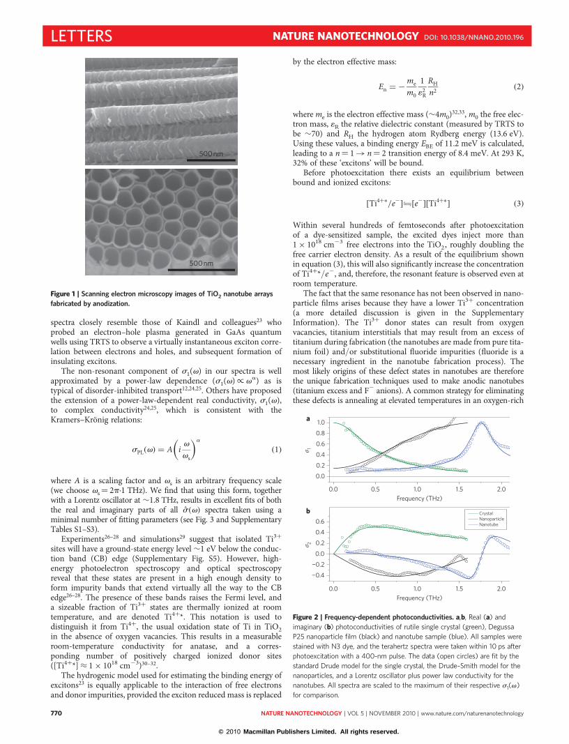
In previous work we obtained the frequency-dependent complexphotoconductivity, s(v) = s1(v) + is2(v), of rutile single crystalsand nanoparticle films over terahertz frequencies12. As can be seenin Fig. 2 the single crystal demonstrates ideal Drude conductivity.On the other hand, anatase and rutile nanoparticle films ofvarious sizes (7–200 nm)12,19,20, as well as ZnO nanoparticle andnanowire films11, do not all conform to classical Drude behavior,but instead demonstrate behaviour that can be consistently fit bythe extended Drude–Smith model12,19,21,22. In all of these samples,the imaginary conductivity, s2(v), is negative at low frequencies,corresponding to a Drude–Smith parameter c close to –1, whichsuggests transport dominated by backscattering and/or disorder-induced localization.
A representative s(v) spectrum for TiO2 nanotubes is alsoshown in Fig. 2. In both the nanotube and nanoparticle samples,d.c. conductivity is suppressed, that is, s1,dc,nano ≪ s1,dc,crystal , asv� 0 (where s1 is the real part of the complex-valued conduc-tivity), suggesting comparably low electron mobility. However, thenanotube spectrum is fundamentally different from that forsingle-crystal or nanoparticulate TiO2, and is dominated by asharp resonance at �1.8 THz (7.5 meV). Even though the exper-imental bandwidth extends only up to 1.6 THz when probing thesingle crystal and nanoparticle samples, it is clear from the lack ofdownward curvature in s2 that no oscillator component ispresent. Furthermore, Tiwana and colleagues recently measuredthe TiO2 nanoparticle photoconductivity spectrum to 2.0 THzand did not observe a resonant feature20 (see SupplementaryInformation for a detailed discussion).
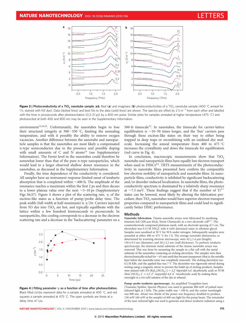
As can be seen in Fig. 3 and the plots in the SupplementaryInformation, the resonance at 1.8 THz is present in all polycrystal-line nanotube samples, whether annealed at 400 8C or 475 8C,whether stained with N3 (also known as red dye) and photoexcitedat 400 nm, or N749 (also known as black dye) and photoexcited at800 nm. The observed resonance can be fit in all spectra by a singleclassical Lorentz oscillator (see Supplementary Information forfitting equations and parameter values obtained). Our s(v)
Department of Chemistry, Yale University, 225 Prospect St., New Haven, Connecticut 06520-8107 USA; †Present address: Rochester Institute ofTechnology, Chemical and Biomedical Engineering, 160 Lomb Memorial Drive, Rochester, New York 14623-5603 USA.
*e-mail: [email protected]
LETTERSPUBLISHED ONLINE: 17 OCTOBER 2010 | DOI: 10.1038/NNANO.2010.196
NATURE NANOTECHNOLOGY | VOL 5 | NOVEMBER 2010 | www.nature.com/naturenanotechnology 769
© 2010 Macmillan Publishers Limited. All rights reserved.
spectra closely resemble those of Kaindl and colleagues23 whoprobed an electron–hole plasma generated in GaAs quantumwells using TRTS to observe a virtually instantaneous exciton corre-lation between electrons and holes, and subsequent formation ofinsulating excitons.
The non-resonant component of s1(v) in our spectra is wellapproximated by a power-law dependence (s1(v)/va) as istypical of disorder-inhibited transport12,24,25. Others have proposedthe extension of a power-law-dependent real conductivity, s1(v),to complex conductivity24,25, which is consistent with theKramers–Kronig relations:
sPL v( ) = A iv
vs
( )a
(1)
where A is a scaling factor and vs is an arbitrary frequency scale(we choose vs¼ 2p.1 THz). We find that using this form, togetherwith a Lorentz oscillator at �1.8 THz, results in excellent fits of boththe real and imaginary parts of all s(v) spectra taken using aminimal number of fitting parameters (see Fig. 3 and SupplementaryTables S1–S3).
Experiments26–28 and simulations29 suggest that isolated Ti3þ
sites will have a ground-state energy level �1 eV below the conduc-tion band (CB) edge (Supplementary Fig. S5). However, high-energy photoelectron spectroscopy and optical spectroscopyreveal that these states are present in a high enough density toform impurity bands that extend virtually all the way to the CBedge26–28. The presence of these bands raises the Fermi level, anda sizeable fraction of Ti3þ states are thermally ionized at roomtemperature, and are denoted Ti4þ*. This notation is used todistinguish it from Ti4þ, the usual oxidation state of Ti in TiO2in the absence of oxygen vacancies. This results in a measurableroom-temperature conductivity for anatase, and a corres-ponding number of positively charged ionized donor sites([Ti4þ*] ≈ 1 × 1018 cm23)30–32.
The hydrogenic model used for estimating the binding energy ofexcitons23 is equally applicable to the interaction of free electronsand donor impurities, provided the exciton reduced mass is replaced
by the electron effective mass:
En = − me
m0
112
R
RH
n2(2)
where me is the electron effective mass (�4m0)32,33, m0 the free elec-tron mass, 1R the relative dielectric constant (measured by TRTS tobe �70) and RH the hydrogen atom Rydberg energy (13.6 eV).Using these values, a binding energy EBE of 11.2 meV is calculated,leading to a n¼ 1 � n¼ 2 transition energy of 8.4 meV. At 293 K,32% of these ‘excitons’ will be bound.
Before photoexcitation there exists an equilibrium betweenbound and ionized excitons:
[Ti4+∗/e−]N[e−][Ti4+∗] (3)
Within several hundreds of femtoseconds after photoexcitationof a dye-sensitized sample, the excited dyes inject more than1 × 1018 cm23 free electrons into the TiO2, roughly doubling thefree carrier electron density. As a result of the equilibrium shownin equation (3), this will also significantly increase the concentrationof Ti4þ*/e2, and, therefore, the resonant feature is observed even atroom temperature.
The fact that the same resonance has not been observed in nano-particle films arises because they have a lower Ti3þ concentration(a more detailed discussion is given in the SupplementaryInformation). The Ti3þ donor states can result from oxygenvacancies, titanium interstitials that may result from an excess oftitanium during fabrication (the nanotubes are made from pure tita-nium foil) and/or substitutional fluoride impurities (fluoride is anecessary ingredient in the nanotube fabrication process). Themost likely origins of these defect states in nanotubes are thereforethe unique fabrication techniques used to make anodic nanotubes(titanium excess and F2 anions). A common strategy for eliminatingthese defects is annealing at elevated temperatures in an oxygen-rich
500 nm
500 nm
Figure 1 | Scanning electron microscopy images of TiO2 nanotube arrays
fabricated by anodization.
0.0 0.5 1.0Frequency (THz)
1.5 2.0
0.0
1.0a
b
0.8
0.6
0.4
0.2
0.0
0.6
0.4
0.2
0.0
−0.2
−0.4
0.5 1.0Frequency (THz)
1.5 2.0
CrystalNanoparticleNanotube
1 2
Figure 2 | Frequency-dependent photoconductivities. a,b, Real (a) and
imaginary (b) photoconductivities of rutile single crystal (green), Degussa
P25 nanoparticle film (black) and nanotube sample (blue). All samples were
stained with N3 dye, and the terahertz spectra were taken within 10 ps after
photoexcitation with a 400-nm pulse. The data (open circles) are fit by the
standard Drude model for the single crystal, the Drude–Smith model for the
nanoparticles, and a Lorentz oscillator plus power law conductivity for the
nanotubes. All spectra are scaled to the maximum of their respective s1(v)
for comparison.
LETTERS NATURE NANOTECHNOLOGY DOI: 10.1038/NNANO.2010.196
NATURE NANOTECHNOLOGY | VOL 5 | NOVEMBER 2010 | www.nature.com/naturenanotechnology770
© 2010 Macmillan Publishers Limited. All rights reserved.
environment14,34,35. Unfortunately, the nanotubes begin to losetheir structural integrity at 5002550 8C, limiting the annealingtemperature, and with it possibly the ability to remove oxygenvacancies. Another difference between the nanotube and nanopar-ticle samples is that the nanotubes are most likely a compensatedn-type semiconductor due to the presence and possible dopingwith small amounts of C and N atoms14 (see SupplementaryInformation). The Fermi level in the nanotubes could therefore besomewhat lower than that of the pure n-type nanoparticles, whichwould lead to a larger observed shallow donor resonance in thenanotubes, as discussed in the Supplementary Information.
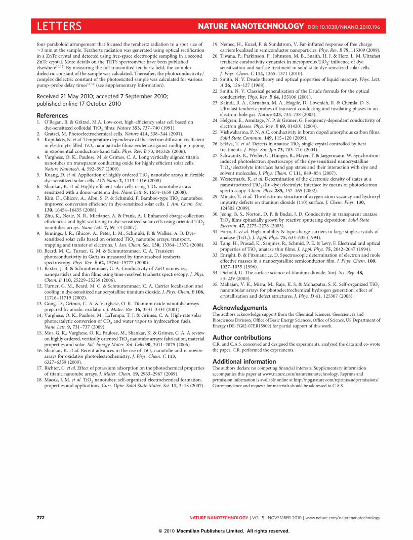
Finally, the time dependence of the conductivity is considered.All samples have an instrument response-limited onset of terahertzabsorption that is completed within �400 fs. The amplitude of theresonance reaches a maximum within the first 2 ps and then decaysto a lower plateau value over the next �5–10 ps (SupplementaryFigs S6,S7). Figure 4 shows a plot of the scattering rate, g, of theexciton-like states as a function of pump/probe delay time. Thepeak width (full-width at half-maximum) is g/2p. Carriers injectedfrom N3 dye into TiO2 are hot, and typically equilibrate with thelattice within a few hundred femtoseconds to picoseconds. Innanoparticles, this cooling corresponds to a decrease in the electronscattering rate and a decrease in the ‘backscattering’ parameter on a
500-fs timescale12. In nanotubes, the timescale for carrier-latticeequilibration is �10–50 times longer, and the ‘free’ carriers passthrough these exciton-like states on their way to either beingtrapped in deep traps or recombining with an oxidized dye mol-ecule. Increasing the anneal temperature from 400 to 475 8Cincreases the crystallinity and slows the timescale for equilibration(red curve in Fig. 4).
In conclusion, macroscopic measurements show that TiO2nanotube and nanoparticle films have equally low electron transportwhen used in DSSCs8,9. TRTS measurements of the photoconduc-tivity in nanotube films presented here confirm the comparablylow electron mobility of nanoparticle and nanotube films. In nano-particle films, conductivity is inhibited by significant backscatteringand/or disorder-induced localization. In nanotube films, the photo-conductivity spectrum is dominated by a relatively sharp resonanceat �7.5 meV. These findings suggest that if the number of Ti3þ
states can be lowered, most likely by altering the fabrication pro-cedure, then TiO2 nanotubes would have superior electron transportproperties compared to nanoparticle films and could lead to signifi-cantly better DSSC performance.
MethodsNanotube fabrication. Titania nanotube arrays were fabricated by anodizingtitanium foil (200 mm thick, Strem Chemicals) in a two-electrode cell8,17. Thecounterelectrode comprised platinum mesh, with an electrode spacing of 5 cm. Theelectrolyte was 0.15 M NH4F, with 6 vol% deionized water in ethylene glycol.Samples were anodized at 50 V for 50 h under nitrogen. Subsequently samples wereannealed at either 400 or 475 8C for 1 h. The average nanotube dimensions, asdetermined by scanning electron microscopy, were 42+1.4 mm (length),150+9.5 nm (diameter) and 28+2.2 nm (wall thickness). To perform terahertzspectroscopy, the titanium metal substrate of the titania nanotube arrays wasremoved. This was done by mounting the sample in a flat cell with the metalsubstrate of the nanotubes contacting an etching electrolyte. The samples were thenelectrochemically etched for�45 min until they became transparent (that is, the metalliclayer below the nanotube array was completely removed). The etching electrolyte was0.2 M KBr, and the applied bias was 7 V. The electrolyte was vigorously stirred duringetching using a magnetic stirrer to prevent the build-up of etching products. Sampleswere stained with N3 (RuL2(NCS)2; L¼ 2,2′-bipyridyl-4,4′-dicarboxylic acid) or N749(RuL′(NCS)3; L′ ¼ 2,2′ ,2′ ′-terpyridyl-4,4′ ,4′ ′-tricarboxylic acid) by soaking themovernight in a 0.6 mM solution of the dye in ethanol.
Pump–probe terahertz spectroscopy. An amplified Ti:sapphire laser(Tsunami/Spitfire, Spectra Physics) was used to generate 800 mW of pulsed near-infrared light at 1 kHz. The pulse width was �100 fs, and the centre wavelengthwas 800 nm. About two-thirds of the power was frequency-doubled to produce150 mW (60 mW at the sample) of 400 nm light for the pump beam. The remainderof the near-infrared light was used to generate and detect terahertz radiation using a
18a b2121
7
2
1
0.75
0.5
0.35
0.2
4
7
4
2
1
0.75
0.5
0.35
0.2
16
14
12
10
8
6
4
1 (S
m−1
)
2 (S
m−1
)
2
0
18
16
14
12
10
8
6
4
2
0
0.5 1.0 1.5 2.0Frequency (THz)
0.5 1.0 1.5 2.0Frequency (THz)
Figure 3 | Photoconductivity of a TiO2 nanotube sample. a,b, Real (a) and imaginary (b) photoconductivities of a TiO2 nanotube sample (400 8C anneal for
1 h, stained with N3 dye). Data (dotted lines) and best fits to the data (solid lines) are shown. The spectra are offset by 2 S m21 from each other and labelled
with the time in picoseconds after photoexcitation (0.2–21 ps) by a 400-nm pulse. Similar plots for samples annealed at higher temperature (475 8C) and
photoexcited at both 400 and 800 nm may be seen in the Supplementary Information.
00.0
0.5
1.0
1.5
(ps
−1)
2.0
2.5
5 10 15 20 25Time (ps)
Figure 4 | Fitting parameter g as a function of time after photoexcitation.
Black filled circles represent data for a sample annealed at 400 8C, and red
squares a sample annealed at 475 8C. The open symbols are those at a
delay time of 1 ps.
NATURE NANOTECHNOLOGY DOI: 10.1038/NNANO.2010.196 LETTERS
NATURE NANOTECHNOLOGY | VOL 5 | NOVEMBER 2010 | www.nature.com/naturenanotechnology 771
© 2010 Macmillan Publishers Limited. All rights reserved.
four-paraboloid arrangement that focused the terahertz radiation to a spot size of�3 mm at the sample. Terahertz radiation was generated using optical rectificationin a ZnTe crystal and detected using free-space electrooptic sampling in a secondZnTe crystal. More details on the TRTS spectrometer have been publishedelsewhere10,12. By measuring the full transmitted terahertz field, the complexdielectric constant of the sample was calculated. Thereafter, the photoconductivity/complex dielectric constant of the photoexcited sample was calculated for variouspump–probe delay times11,12 (see Supplementary Information).
Received 21 May 2010; accepted 7 September 2010;published online 17 October 2010
References1. O’Regan, B. & Gratzel, M.A. Low-cost, high-efficiency solar cell based on
dye-sensitized colloidal TiO2 films. Nature 353, 737–740 (1991).2. Gratzel, M. Photoelectrochemical cells. Nature 414, 338–344 (2001).3. Kopidakis, N. et al. Temperature dependence of the electron diffusion coefficient
in electrolyte-filled TiO2 nanoparticle films: evidence against multiple trappingin exponential conduction-band tails. Phys. Rev. B 73, 045326 (2006).
4. Varghese, O. K., Paulose, M. & Grimes, C. A. Long vertically aligned titaniananotubes on transparent conducting oxide for highly efficient solar cells.Nature Nanotech. 4, 592–597 (2009).
5. Kuang, D. et al. Application of highly ordered TiO2 nanotube arrays in flexibledye-sensitized solar cells. ACS Nano 2, 1113–1116 (2008).
6. Shankar, K. et al. Highly efficient solar cells using TiO2 nanotube arrayssensitized with a donor-antenna dye. Nano Lett. 8, 1654–1659 (2008).
7. Kim, D., Ghicov, A., Albu, S. P. & Schmuki, P. Bamboo-type TiO2 nanotubes:improved conversion efficiency in dye-sensitized solar cells. J. Am. Chem. Soc.130, 16454–16455 (2008).
8. Zhu, K., Neale, N. R., Miedaner, A. & Frank, A. J. Enhanced charge-collectionefficiencies and light scattering in dye-sensitized solar cells using oriented TiO2nanotubes arrays. Nano Lett. 7, 69–74 (2007).
9. Jennings, J. R., Ghicov, A., Peter, L. M., Schmuki, P. & Walker, A. B. Dye-sensitized solar cells based on oriented TiO2 nanotube arrays: transport,trapping and transfer of electrons. J. Am. Chem. Soc. 130, 13364–13372 (2008).
10. Beard, M. C., Turner, G. M. & Schmuttenmaer, C. A. Transientphotoconductivity in GaAs as measured by time-resolved terahertzspectroscopy. Phys. Rev. B 62, 15764–15777 (2000).
11. Baxter, J. B. & Schmuttenmaer, C. A. Conductivity of ZnO nanowires,nanoparticles and thin films using time-resolved terahertz spectroscopy. J. Phys.Chem. B 110, 25229–25239 (2006).
12. Turner, G. M., Beard, M. C. & Schmuttenmaer, C. A. Carrier localization andcooling in dye-sensitized nanocrystalline titanium dioxide. J. Phys. Chem. B 106,11716–11719 (2002).
13. Gong, D., Grimes, C. A. & Varghese, O. K. Titanium oxide nanotube arraysprepared by anodic oxidation. J. Mater. Res. 16, 3331–3334 (2001).
14. Varghese, O. K., Paulose, M., LaTempa, T. J. & Grimes, C. A. High-rate solarphotocatalytic conversion of CO2 and water vapor to hydrocarbon fuels.Nano Lett. 9, 731–737 (2009).
15. Mor, G. K., Varghese, O. K., Paulose, M., Shankar, K. & Grimes, C. A. A reviewon highly ordered, vertically oriented TiO2 nanotube arrays: fabrication, materialproperties and solar. Sol. Energy Mater. Sol. Cells 90, 2011–2075 (2006).
16. Shankar, K. et al. Recent advances in the use of TiO2 nanotube and nanowirearrays for oxidative photoelectrochemistry. J. Phys. Chem. C 113,6327–6359 (2009).
17. Richter, C. et al. Effect of potassium adsorption on the photochemical propertiesof titania nanotube arrays. J. Mater. Chem. 19, 2963–2967 (2009).
18. Macak, J. M. et al. TiO2 nanotubes: self-organized electrochemical formation,properties and applications. Curr. Opin. Solid State Mater. Sci. 11, 3–18 (2007).
19. Nemec, H., Kuzel, P. & Sundstrom, V. Far-infrared response of free chargecarriers localized in semiconductor nanoparticles. Phys. Rev. B 79, 115309 (2009).
20. Tiwana, P., Parkinson, P., Johnston, M. B., Snaith, H. J. & Herz, L. M. Ultrafastterahertz conductivity dynamics in mesoporous TiO2: influence of dyesensitization and surface treatment in solid-state dye-sensitized solar cells.J. Phys. Chem. C 114, 1365–1371 (2010).
21. Smith, N. V. Drude theory and optical properties of liquid mercury. Phys. Lett.A 26, 126–127 (1968).
22. Smith, N. V. Classical generalization of the Drude formula for the opticalconductivity. Phys. Rev. B 64, 155106 (2001).
23. Kaindl, R. A., Carnahan, M. A., Hagele, D., Lovenich, R. & Chemla, D. S.Ultrafast terahertz probes of transient conducting and insulating phases in anelectron–hole gas. Nature 423, 734–738 (2003).
24. Helgren, E., Armitage, N. P. & Gruner, G. Frequency-dependent conductivity ofelectron glasses. Phys. Rev. B 69, 014201 (2004).
25. Vishwakarma, P. N. A.C. conductivity in boron doped amorphous carbon films.Solid State Commun. 149, 115–120 (2009).
26. Sekiya, T. et al. Defects in anatase TiO2 single crystal controlled by heattreatments. J. Phys. Soc. Jpn 73, 703–710 (2004).
27. Schwanitz, K., Weiler, U., Hunger, R., Mayer, T. & Jaegermann, W. Synchrotron-induced photoelectron spectroscopy of the dye-sensitized nanocrystallineTiO2/electrolyte interface: band gap states and their interaction with dye andsolvent molecules. J. Phys. Chem. C 111, 849–854 (2007).
28. Westermark, K. et al. Determination of the electronic density of states at ananostructured TiO2/Ru-dye/electrolyte interface by means of photoelectronspectroscopy. Chem. Phys. 285, 157–165 (2002).
29. Minato, T. et al. The electronic structure of oxygen atom vacancy and hydroxylimpurity defects on titanium dioxide (110) surface. J. Chem. Phys. 130,124502 (2009).
30. Jeong, B. S., Norton, D. P. & Budai, J. D. Conductivity in transparent anataseTiO2 films epitaxially grown by reactive sputtering deposition. Solid StateElectron. 47, 2275–2278 (2003).
31. Forro, L. et al. High-mobility N-type charge-carriers in large single-crystals ofanatase (TiO2). J. Appl. Phys. 75, 633–635 (1994).
32. Tang, H., Prasad, K., Sanjines, R., Schmid, P. E. & Levy, F. Electrical and opticalproperties of TiO2 anatase thin films. J. Appl. Phys. 75, 2042–2047 (1994).
33. Enright, B. & Fitzmaurice, D. Spectroscopic determination of electron and moleeffective masses in a nanocrystalline semiconductor film. J. Phys. Chem. 100,1027–1035 (1996).
34. Diebold, U. The surface science of titanium dioxide. Surf. Sci. Rep. 48,53–229 (2003).
35. Mahajan, V. K., Misra, M., Raja, K. S. & Mohapatra, S. K. Self-organized TiO2nanotubular arrays for photoelectrochemical hydrogen generation: effect ofcrystallization and defect structures. J. Phys. D 41, 125307 (2008).
AcknowledgementsThe authors acknowledge support from the Chemical Sciences, Geosciences andBiosciences Division, Office of Basic Energy Sciences, Office of Science, US Department ofEnergy (DE-FG02-07ER15909) for partial support of this work.
Author contributionsC.R. and C.A.S. conceived and designed the experiments, analysed the data and co-wrotethe paper. C.R. performed the experiments.
Additional informationThe authors declare no competing financial interests. Supplementary informationaccompanies this paper at www.nature.com/naturenanotechnology. Reprints andpermission information is available online at http://npg.nature.com/reprintsandpermissions/.Correspondence and requests for materials should be addressed to C.A.S.
LETTERS NATURE NANOTECHNOLOGY DOI: 10.1038/NNANO.2010.196
NATURE NANOTECHNOLOGY | VOL 5 | NOVEMBER 2010 | www.nature.com/naturenanotechnology772
© 2010 Macmillan Publishers Limited. All rights reserved.

SUPPLEMENTARY INFORMATIONdoi: 10.1038/nnano.2010.196
nature nanotechnology | www.nature.com/naturenanotechnology 1
1
Supplementary Information for:
Exciton-like trap states limit electron mobility in TiO2 nanotubes
Christiaan Richter and Charles A. Schmuttenmaer*
*Electronic mail: [email protected]
July 28, 2010 Contents Page 2. Figure S1: A schematic representation of the electronic defect structure of TiO2.
Page 2. Figure S2: Side view Scanning Electron Microscopy image of a nanotube sample.
Page 3. Equations used to fit the data.
Page 5. Table S1: Fitting parameters for NTs annealed at 400 C, sensitized with red dye.
Page 6. Figure S3: Conductivity for NTs annealed at 475 C and sensitized with red dye.
Page 6. Table S2: Fitting parameters for NTs annealed at 475 C and sensitized with red dye.
Page 7. Figure S4: Conductivity for NTs annealed at 475 C and sensitized with black dye.
Page 7. Table S3: Fitting parameters for NTs annealed at 475 C and sensitized with black dye.
Page 8. Anatase energy level diagram.
Page 9. Temporal evolution of the resonant peak at ~1.8 THz.
Page 12. Differences between NTs and NPs.
Page 14. Relevance to DSSCs.
Page 15. Time-resolved terahertz spectroscopy applied to nanostructured materials.
Page 17. References.
© 2010 Macmillan Publishers Limited. All rights reserved.
2 nature nanotechnology | www.nature.com/naturenanotechnology
SUPPLEMENTARY INFORMATION doi: 10.1038/nnano.2010.196
2
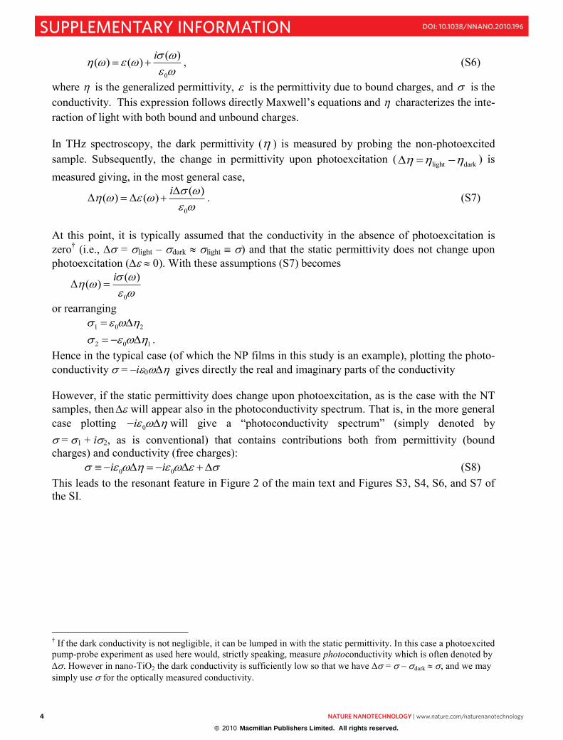
Figure S2. A side-view SEM image of a NT sample. The open „top-side‟ of the nanotube array is on the left of the image.
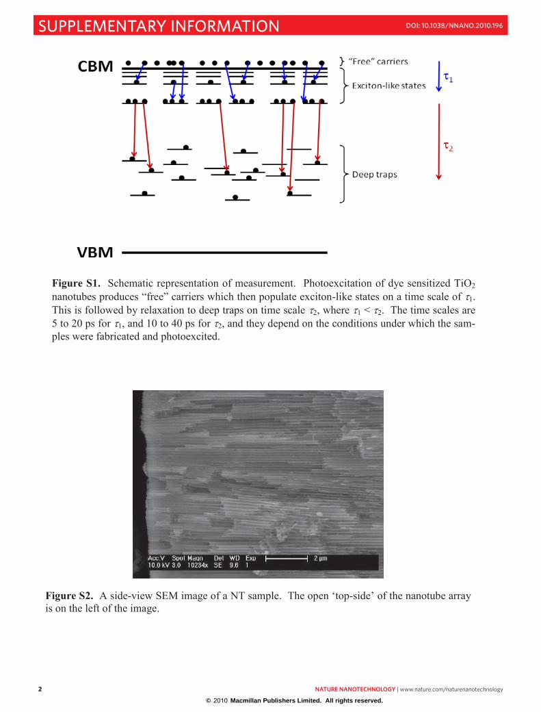
Figure S1. Schematic representation of measurement. Photoexcitation of dye sensitized TiO2 nanotubes produces “free” carriers which then populate exciton-like states on a time scale of 1. This is followed by relaxation to deep traps on time scale 2, where 1 <2. The time scales are 5 to 20 ps for 1, and 10 to 40 ps for 2, and they depend on the conditions under which the sam-ples were fabricated and photoexcited.
© 2010 Macmillan Publishers Limited. All rights reserved.

nature nanotechnology | www.nature.com/naturenanotechnology 3
SUPPLEMENTARY INFORMATIONdoi: 10.1038/nnano.2010.196
3
Fitting equations and parameters The equations used to model the data are given here. The parameter values obtained for samples prepared and/or probed under different conditions are given in Tables S1 – S3. Drude conductivity1,2
2
00 * where
1e
Drudee
N ei m
(S1)
Where is frequency (rad/s), is scattering time, i is unit imaginary, Ne is electron density, e is the charge of an electron, and me* is the carrier‟s effective mass. The Drude model is the sim-plest model of conductivity. It assumes complete momentum randomization after each scattering event. Drude-Smith conductivity3
0 1 1,1 1 1DS
c ci i
(S2)
There is a single parameter, c, beyond the standard Drude model, which is referred to as the per-sistence of velocity parameter. When c = 0, the Drude model is recovered. When c approaches –1, the low frequency and DC conductivity is suppressed, and the imaginary conductivity be-comes negative at intermediate frequencies. Power law conductivity4
s
PL A i
(S3)
This is a Kramers-Kroning consistent implementation of power law behavior where s is an arbi-trary frequency scale. Here we choose s = 21 THz. Lorentz oscillator2
20
2 20
LO R i
(S4)
with RL . Where L is the relative dielectric constant for << 0 and R is the rela-tive dielectric constant for >> 0. If there are no additional resonant features between the re-sonant frequency and DC then L = DC. In the hypothetical situation where there are no addi-tional resonant features for > 0 then R would be ( as ). For a classical Co-loumbic Lorentz oscillator between two charges e, the oscillator strength is given by:2
2
20 0
os
e
N em
(S5)
where Nos is the number density of oscillators, and me in general is the reduced mass of the oscil-lator. In our case, assuming a stationary Ti4+* entity, me is the electron effective mass in anatase. In the limit of 0 much greater than , the full width at half maximum (FWHM) of the peak is given by2 FWHM = / 2. 0 is the permittivity of free space. Note that the Lorentz oscillator is not a conductivity model, but will manifest itself in the photo-conductivity spectrum through the relation5
© 2010 Macmillan Publishers Limited. All rights reserved.
4 nature nanotechnology | www.nature.com/naturenanotechnology
SUPPLEMENTARY INFORMATION doi: 10.1038/nnano.2010.196
4
0
( )( ) ( ) i
, (S6)
where is the generalized permittivity, is the permittivity due to bound charges, and is the conductivity. This expression follows directly Maxwell‟s equations and characterizes the inte-raction of light with both bound and unbound charges. In THz spectroscopy, the dark permittivity ( ) is measured by probing the non-photoexcited sample. Subsequently, the change in permittivity upon photoexcitation ( light dark ) is measured giving, in the most general case,
0
( )( ) ( ) i
. (S7)
At this point, it is typically assumed that the conductivity in the absence of photoexcitation is zero† (i.e., = light – dark light ) and that the static permittivity does not change upon photoexcitation ( 0). With these assumptions (S7) becomes
0
( )( ) i
or rearranging 1 0 2
2 0 1 . Hence in the typical case (of which the NP films in this study is an example), plotting the photo-conductivity = –i0 gives directly the real and imaginary parts of the conductivity However, if the static permittivity does change upon photoexcitation, as is the case with the NT samples, then will appear also in the photoconductivity spectrum. That is, in the more general case plotting 0i will give a “photoconductivity spectrum” (simply denoted by = 1 + i2, as is conventional) that contains contributions both from permittivity (bound charges) and conductivity (free charges):
0 0i i (S8) This leads to the resonant feature in Figure 2 of the main text and Figures S3, S4, S6, and S7 of the SI.
† If the dark conductivity is not negligible, it can be lumped in with the static permittivity. In this case a photoexcited pump-probe experiment as used here would, strictly speaking, measure photoconductivity which is often denoted by . However in nano-TiO2 the dark conductivity is sufficiently low so that we have = – dark , and we may simply use for the optically measured conductivity.
© 2010 Macmillan Publishers Limited. All rights reserved.

nature nanotechnology | www.nature.com/naturenanotechnology 5
SUPPLEMENTARY INFORMATIONdoi: 10.1038/nnano.2010.196
5
Fitting parameters (400 ºC with red dye) Using PL (Equation S3) and a Lorentz oscillator (Equation S4), the fitting parameters corres-ponding to Figure 3 of the main text (sample annealed at 400 ºC for 6 h and stained with N3 dye) are given in Table S1.
time (ps) (THz THz R A (S/m) Nos 1014 cm-3 0.2 1.851779 0.841849 0.001047 0.014 0.624373 0.638153 1.781354 0.35 1.842975 1.458294 0.00225 0.014 0.841089 0.484984 3.791307 0.5 1.794364 1.36422 0.002179 0.014 1.074229 0.407041 3.48071 0.75 1.799049 1.775081 0.003632 0.014 0.946022 0.296839 5.833004 1 1.765041 1.837472 0.005219 0.014 0.805161 0.485939 8.067931 2 1.755998 2.069118 0.006774 0.014 1.012724 0.558507 10.36405 4 1.782484 2.446978 0.006141 0.014 0.838482 0.412029 9.680538 7 1.745165 2.677314 0.005399 0.014 0.55025 0.446933 8.159263 21 1.782018 1.931302 0.003617 0.014 0.582213 0.471728 5.698698
Table S1. Parameters obtained using Equations S3 and S4. The apparent oscillator density (Nos) is calculated using Equation S5 and an electron effective mass of 4 m0. The value of R was held fixed during fitting procedure.
© 2010 Macmillan Publishers Limited. All rights reserved.
6 nature nanotechnology | www.nature.com/naturenanotechnology
SUPPLEMENTARY INFORMATION doi: 10.1038/nnano.2010.196
6
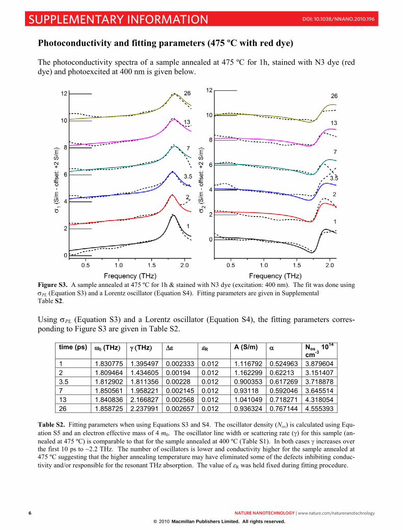
Photoconductivity and fitting parameters (475 ºC with red dye) The photoconductivity spectra of a sample annealed at 475 ºC for 1h, stained with N3 dye (red dye) and photoexcited at 400 nm is given below.
Figure S3. A sample annealed at 475 ºC for 1h & stained with N3 dye (excitation: 400 nm). The fit was done using PL (Equation S3) and a Lorentz oscillator (Equation S4). Fitting parameters are given in Supplemental Table S2. Using PL (Equation S3) and a Lorentz oscillator (Equation S4), the fitting parameters corres-ponding to Figure S3 are given in Table S2.
time (ps) (THz THz R A (S/m) Nos 1014
cm-31 1.830775 1.395497 0.002333 0.012 1.116792 0.524963 3.879604 2 1.809464 1.434605 0.00194 0.012 1.162299 0.62213 3.151407 3.5 1.812902 1.811356 0.00228 0.012 0.900353 0.617269 3.718878 7 1.850561 1.958221 0.002145 0.012 0.93118 0.592046 3.645514 13 1.840836 2.166827 0.002568 0.012 1.041049 0.718271 4.318054 26 1.858725 2.237991 0.002657 0.012 0.936324 0.767144 4.555393
Table S2. Fitting parameters when using Equations S3 and S4. The oscillator density (Nos) is calculated using Equ-ation S5 and an electron effective mass of 4 m0. The oscillator line width or scattering rate () for this sample (an-nealed at 475 ºC) is comparable to that for the sample annealed at 400 ºC (Table S1). In both cases increases over the first 10 ps to ~2.2 THz. The number of oscillators is lower and conductivity higher for the sample annealed at 475 ºC suggesting that the higher annealing temperature may have eliminated some of the defects inhibiting conduc-tivity and/or responsible for the resonant THz absorption. The value of R was held fixed during fitting procedure.
© 2010 Macmillan Publishers Limited. All rights reserved.
nature nanotechnology | www.nature.com/naturenanotechnology 7
SUPPLEMENTARY INFORMATIONdoi: 10.1038/nnano.2010.196
7
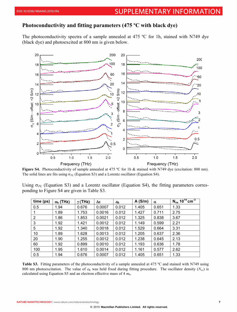
Photoconductivity and fitting parameters (475 ºC with black dye) The photoconductivity spectra of a sample annealed at 475 ºC for 1h, stained with N749 dye (black dye) and photoexcited at 800 nm is given below.
Figure S4. Photoconductivity of sample annealed at 475 ºC for 1h & stained with N749 dye (excitation: 800 nm). The solid lines are fits using PL (Equation S3) and a Lorentz oscillator (Equation S4). Using PL (Equation S3) and a Lorentz oscillator (Equation S4), the fitting parameters corres-ponding to Figure S4 are given in Table S3.
time (ps) (THz THz R A (S/m) Nos 1014 cm-30.5 1.94 0.676 0.0007 0.012 1.405 0.651 1.33 1 1.89 1.753 0.0016 0.012 1.427 0.711 2.75 2 1.86 1.853 0.0021 0.012 1.325 0.838 3.67 3 1.92 1.421 0.0012 0.012 1.149 0.599 2.21 5 1.92 1.340 0.0018 0.012 1.529 0.664 3.31 10 1.89 1.628 0.0013 0.012 1.205 0.637 2.36 20 1.90 1.255 0.0012 0.012 1.238 0.645 2.13 60 1.92 0.899 0.0010 0.012 1.193 0.636 1.78 100 1.95 1.610 0.0014 0.012 1.161 0.577 2.62 0.5 1.94 0.676 0.0007 0.012 1.405 0.651 1.33
Table S3. Fitting parameters of the photoconductivity of a sample annealed at 475 ºC and stained with N749 using 800 nm photoexcitation. The value of R was held fixed during fitting procedure. The oscillator density (Nos) is calculated using Equation S5 and an electron effective mass of 4 m0.
© 2010 Macmillan Publishers Limited. All rights reserved.
8 nature nanotechnology | www.nature.com/naturenanotechnology
SUPPLEMENTARY INFORMATION doi: 10.1038/nnano.2010.196
8
Anatase energy level diagram
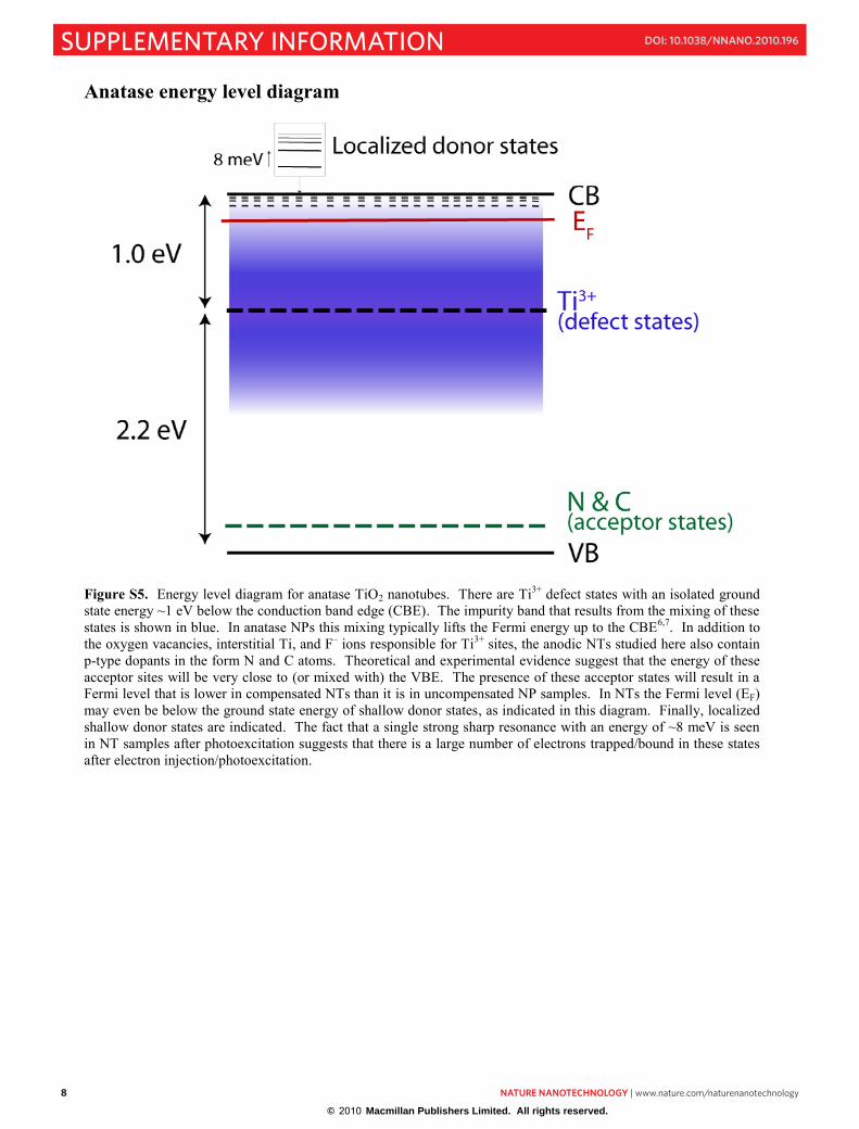
Figure S5. Energy level diagram for anatase TiO2 nanotubes. There are Ti3+ defect states with an isolated ground state energy ~1 eV below the conduction band edge (CBE). The impurity band that results from the mixing of these states is shown in blue. In anatase NPs this mixing typically lifts the Fermi energy up to the CBE6,7. In addition to the oxygen vacancies, interstitial Ti, and F– ions responsible for Ti3+ sites, the anodic NTs studied here also contain p-type dopants in the form N and C atoms. Theoretical and experimental evidence suggest that the energy of these acceptor sites will be very close to (or mixed with) the VBE. The presence of these acceptor states will result in a Fermi level that is lower in compensated NTs than it is in uncompensated NP samples. In NTs the Fermi level (EF) may even be below the ground state energy of shallow donor states, as indicated in this diagram. Finally, localized shallow donor states are indicated. The fact that a single strong sharp resonance with an energy of ~8 meV is seen in NT samples after photoexcitation suggests that there is a large number of electrons trapped/bound in these states after electron injection/photoexcitation.
© 2010 Macmillan Publishers Limited. All rights reserved.

nature nanotechnology | www.nature.com/naturenanotechnology 9
SUPPLEMENTARY INFORMATIONdoi: 10.1038/nnano.2010.196
9
Temporal evolution of the resonant peak at ~1.8 THz The resonance in the photoconductivity spectra of all N3 dye stained samples show relaxation dynamics illustrated in Figures S6 and S7. As seen in Figure S6, the resonance in the real con-ductivity at around 1.8 THz rapidly reaches a maximum within less than 2 ps after photoexcita-tion, and then subsequently relaxes to a plateau value just under two thirds the maximum over the next 10 ps.
Figure S6. A 3D plot of the real part of photoconductivity of the NT sample annealed at 400 oC, stained with red dye, and photoexcited with 400 nm pump pulse at pump-probe delay time = 0 ps. Note that the resonance at 1.8 THz rapidly reaches a peak value within 1 to 2 ps. Figure S7 shows a cut through this surface at ~1.8 THz for the samples annealed at 400 oC and 475 oC. The exact frequency chosen for each sample is that which corresponds to the peak value of the real conductivity. They have been normalized for easier comparison, but the inset shows the non-normalized spectra where it is seen that the sample annealed at 400 oC has a slightly larger peak value. Also, this figure differs from Figure 4 in the main text in that Figure S7 is simply a cut through the time-dependent real conductivity at ~1.8 THz, while Figure 4 is the val-ue of , the scattering rate parameter for the Lorentzian oscillator (as given in Equation S4), found in Tables S1 and S2. Difference in resonant peak intensity as a function of annealing temperature As seen in the inset in Figure S7, the resonant feature in the photoconductivity spectrum of NT samples annealed at 400 ºC is more intense (1,max() = 4.4 S/m) than that of samples annealed at 475 ºC (1,max() = 3.0 S/m).
© 2010 Macmillan Publishers Limited. All rights reserved.

10 nature nanotechnology | www.nature.com/naturenanotechnology
SUPPLEMENTARY INFORMATION doi: 10.1038/nnano.2010.196
10
Figure S7. The normalized peak intensity of 1() (at 0 1.8 THz) as a function of time after photoexcitation. The samples are NT films stained with N3 dye after annealing at 400 ºC (red circles) or 475 ºC (blue triangles). The inset shows 1() for each sample at the delay time when the resonant peak is at its maximum (~2 ps for both sam-ples). The vertical axis of the inset is 1() in S/m and the horizontal axis is frequency in THz. By combining Equations S4 and S8, and separating real and imaginary parts we see that:
1 0 2 1
0 ,2 PL,1
0 ,2 0 PL
22 0
0 20
(using the LO and PL models described above )
for (neglecting the contribution from )
LO
LO
22
.
The resonant peak occurs when = 0, and its height will be given by:
2
0 01 0
.
Upon substitution of Equation S5, one obtains
2
1 0os
e
N em
. (S9)
It can be seen in Figure 4 (or tables S1 and S2) that is larger for samples annealed at 400 C than for samples annealed at 475 C. Therefore, the average lifetime of oscillators within the first 20 ps after carrier injection is shorter in the less crystalline/ordered material (400 C) than in the material annealed at 475 C. However, through Equation S9, this also suggests that the reso-nant peak height for the 400 C annealed samples should be lower than the peak for the 475 C annealed samples. This however is not the case (as can be seen in the inset of Figure S7). The decrease in peak intensity due to broadening is more than offset by the 400 C samples also hav-ing a higher defect density, and hence oscillator density: Nos,400 C 10 1014 cm-3 compared to Nos,475 C 3 1014 cm-3 (see Tables S1 and S2).
© 2010 Macmillan Publishers Limited. All rights reserved.

nature nanotechnology | www.nature.com/naturenanotechnology 11
SUPPLEMENTARY INFORMATIONdoi: 10.1038/nnano.2010.196
11
Thus, samples annealed at lower temperature have 1) a higher defect density that results in a higher a density of oscillator states, with 2) shorter lifetimes/higher scattering rates, and 3) faster equilibration between the lattice, defect states and injected hot carriers (see Figure 4).
© 2010 Macmillan Publishers Limited. All rights reserved.
12 nature nanotechnology | www.nature.com/naturenanotechnology
SUPPLEMENTARY INFORMATION doi: 10.1038/nnano.2010.196
12
Differences between NTs and NPs The differences in their spectra are real As can be seen in the spectra given in Figure 2 of the main text, we are able to reliably measure the nanoparticle (NP) spectra up to 1.6 THz and the nanotube (NT) spectra up to 2.1 THz. The reason for this difference in spectral coverage is that we are able to fabricate free standing NT films. In contrast, the NP films are supported on 150 m thick microscope slide cover-slips made of borosilicate glass. The associated reflection and absorption, which increases rapidly with increasing frequency, limits the bandwidth with which we can probe the NP films. It may be tempting to assert that there could be a peak in the NP spectrum, and we simply do not have enough bandwidth to observe it. However, this is not the case. As can be seen in the NT spectrum in Figure 2 of the main text, a sharp resonance centered at 1.8 THz requires that the imaginary conductivity, 2,NP(), be negative and have negative slope over all frequencies up to 1.6 THz. This is simply not observed in the spectrum of the NP sample. All NP films probed to date by us and others8-15 do not show this behavior that would be consis-tent with the presence of a resonance but instead have characteristic Drude-Smith behavior; that is 2,NP() has a minimum at the same frequency that 1,NP() has its inflection point. These qu-alitative observations are confirmed by the excellent match of the very different conductivity models and the measured spectra (between Drude-Smith and the NP data and Lorentz oscillator and the NT data) as presented in the manuscript. Attempts to model the NP spectra with a Lo-rentz oscillator model fail miserably. When performing TRTS, one is seldom fortunate enough to have the central frequency of a reso-nant feature fall within the accessible spectroscopic window as it does for the NT samples (nota-ble exceptions are excitons in GaAs quantum wells16,17 and in Cu2O18). In fact, it is relatively common to infer the existence of resonances with a central frequency at significantly higher fre-quencies than the spectroscopically accessible spectral region. An example is the detection of excitons in ZnO that has a FIR resonance centered at ~8 THz, the presence of which is clearly seen in spectra taken only over the region 0.35 – 1.45 THz19. In the light of these considerations, it is clear that the photoconductivity spectra of the NT samples have a significant resonance cen-tered at 1.8 THz and the NP samples do not (or if such resonance exists, it is a factor of 30 or more smaller than in the NTs). Lastly, and perhaps most importantly, the absence of a peak in the conductivity spectrum of NP films is confirmed by a recently published study15. Tiwana et al. probed anatase NP films with TRTS on a Z-cut quartz substrate, which absorbs far less strongly than glass, and obtained spec-tra up to 2 THz. Their published spectrum indeed conforms to Drude-Smith behavior in perfect agreement with our spectra, and has no resonance either at 1.8 THz or anywhere else within the 0.2 – 2 THz spectral range probed. The Fermi level and ‘dark’ resonant population To first order, the intensity of a resonant feature in the photoconductivity spectrum depends on the population of resonant species. However, more precisely, the intensity in the photoconduc-tivity spectrum ( ˆ light dark ) of an exciton-like species such as Ti4+*/e– scales with the in-crease of the Ti4+*/e– population upon photoexcitation. Hence the equilibrium populations of
© 2010 Macmillan Publishers Limited. All rights reserved.
nature nanotechnology | www.nature.com/naturenanotechnology 13
SUPPLEMENTARY INFORMATIONdoi: 10.1038/nnano.2010.196
13
this species in the dark will also impact the intensity of an observed resonance. If the dark Fermi level is much higher than the Ti4+*/e– binding energy (EF > CBE), then most Ti4+* states will al-ready be reduced in the dark, resulting in very little further enhancement of any of their reson-ances upon electron injection/photoexcitation since [Ti4+*/e–]dark [Ti4+*/e–]photo-excited. Therefore, in the case of EF > CBE there will be no resonance in the photoconductivity spectrum, even if the Ti3+ density is substantial. Presence of p-type dopants in NTs The ~1.8 THz resonance observed in all TiO2 NT samples has not been observed in any TiO2 NP films. This suggests that NPs have a lower Ti3+ state density compared to NTs. As discussed in the main text, the most likely reasons that the NTs have higher Ti3+ state concentrations lie in their unique fabrication conditions. However, as described in the previous paragraph, the inten-sity of a resonance in the photoconductivity spectrum also depends on the dark equilibrium popu-lation of the resonant state, which in turn depends on the dark Fermi level. In addition to the n-type donor defects discussed in the main text, the NTs also contain small amounts of the p-type dopants nitrogen and carbon. Elemental analysis (see SI in McNamara et al.20 for experimental procedures) of the annealed NT samples prior to sensitization revealed roughly 0.12 wt% C and ~0.03 wt% N (consistent with the findings of Varghese et al.21). Some of these atoms may be present in the form of substitutional nitrogen and/or carbon.21-23 There-fore, anodic titania NTs fabricated in organic electrolytes may have a Fermi level somewhat lower than that of a typical NP film. NP films, which are generally pure n-type, have an experi-mentally observed dark Fermi level that usually resides slightly above the CBE6,7. Thus one would expect a relatively high fraction of any Ti4+* states present in NPs to be reduced, even in the dark. If the NTs on the other hand are a compensated n-type semiconductor, this could lead to the NTs having a lower dark Fermi level compared to NPs, and therefore a more strongly en-hanced resonance in their photoconductivity spectrum.
© 2010 Macmillan Publishers Limited. All rights reserved.
14 nature nanotechnology | www.nature.com/naturenanotechnology
SUPPLEMENTARY INFORMATION doi: 10.1038/nnano.2010.196
14
Relevance to DSSCs In contrast to dry films probed in this study, photoanodes in functioning DSSCs are immersed in a redox electrolyte, and the dark Fermi level in functioning DSSCs is determined by the iodide/triiodide couple24. How relevant are the insights obtained by probing dry films using TRTS to actual DSSCs? Furthermore, how important are the shallow traps in the NTs that are not present in the NPs? The injected electron density immediately after photo-excitation in our experiments (~1 1017 – 5 1017 cm-3) compare well with the extracted electron density in NP films in working DSSCs (~3 1017 cm-3 at short circuit and ~3 1018 cm-3 at open circuit)25. This suggests that the occu-pancy level of these shallow donor sites in our experiments most likely is comparable to those in actual cells. In fact, we recently showed that the injection efficiency measured by TRTS and DSSC efficiency were proportional to each other for films made with varying amounts of anatase and rutile26. When comparing NP films stained with different dyes, we typically find that the injection efficiency measured by TRTS correlates very strongly with DSSC efficiency. Although macroscopic experiments reveal similar electron extraction times for NTs and NPs27,28 the measured electron lifetimes are considerably longer in NTs compared to NPs28-30. It is con-ceivable that the same interaction with shallow donor sites that suppresses electron mobility also may play a role in reducing the rate of electron scavenging by species in the electrolyte by in ef-fect increasing the NTs own “affinity” for electrons. Working DSSCs employing either one of these nanomaterials have remarkably high carrier col-lection efficiencies (90-99%)31. The reason for this is that the recombination processes in DSSCs are even slower than the slow electron transfer (e.g. at ~1 sun typical measured values for the electron extraction time, c, are about 1 ms, and about 10 – 100 ms for the average elec-tron lifetime, r
24,27,28,31,32. Since collection efficiencies are already very high it is therefore not a given that improving the electron transport properties of either NT or NP films would necessarily result in a marked increase in cell performance. However, the state-of-the-art DSSC (TiO2 NP diameter of about nm, triiodide/iodide redox couple, N719 or a close variant as the dye, additives like tert-butylpyridine etc.) has been highly refined over the years, and it would not be expected that radically changing any single component while leaving the others the same would result in a better DSSC. On the other hand, should a new nanomaterial be capable of electron transport that is orders of magnitude faster than its predecessors, such as TiO2 NTs free of these shallow traps, it could conceivably become part of a new dye, redox couple, electrolyte and photoanode system specifically designed to exploit this property.
© 2010 Macmillan Publishers Limited. All rights reserved.
nature nanotechnology | www.nature.com/naturenanotechnology 15
SUPPLEMENTARY INFORMATIONdoi: 10.1038/nnano.2010.196
15
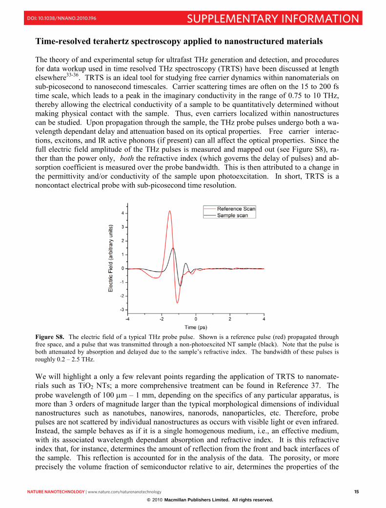
Time-resolved terahertz spectroscopy applied to nanostructured materials The theory of and experimental setup for ultrafast THz generation and detection, and procedures for data workup used in time resolved THz spectroscopy (TRTS) have been discussed at length elsewhere33-36. TRTS is an ideal tool for studying free carrier dynamics within nanomaterials on sub-picosecond to nanosecond timescales. Carrier scattering times are often on the 15 to 200 fs time scale, which leads to a peak in the imaginary conductivity in the range of 0.75 to 10 THz, thereby allowing the electrical conductivity of a sample to be quantitatively determined without making physical contact with the sample. Thus, even carriers localized within nanostructures can be studied. Upon propagation through the sample, the THz probe pulses undergo both a wa-velength dependant delay and attenuation based on its optical properties. Free carrier interac-tions, excitons, and IR active phonons (if present) can all affect the optical properties. Since the full electric field amplitude of the THz pulses is measured and mapped out (see Figure S8), ra-ther than the power only, both the refractive index (which governs the delay of pulses) and ab-sorption coefficient is measured over the probe bandwidth. This is then attributed to a change in the permittivity and/or conductivity of the sample upon photoexcitation. In short, TRTS is a noncontact electrical probe with sub-picosecond time resolution.
Figure S8. The electric field of a typical THz probe pulse. Shown is a reference pulse (red) propagated through free space, and a pulse that was transmitted through a non-photoexcited NT sample (black). Note that the pulse is both attenuated by absorption and delayed due to the sample‟s refractive index. The bandwidth of these pulses is roughly 0.2 – 2.5 THz. We will highlight a only a few relevant points regarding the application of TRTS to nanomate-rials such as TiO2 NTs; a more comprehensive treatment can be found in Reference 37. The probe wavelength of 100 m – 1 mm, depending on the specifics of any particular apparatus, is more than 3 orders of magnitude larger than the typical morphological dimensions of individual nanostructures such as nanotubes, nanowires, nanorods, nanoparticles, etc. Therefore, probe pulses are not scattered by individual nanostructures as occurs with visible light or even infrared. Instead, the sample behaves as if it is a single homogenous medium, i.e., an effective medium, with its associated wavelength dependant absorption and refractive index. It is this refractive index that, for instance, determines the amount of reflection from the front and back interfaces of the sample. This reflection is accounted for in the analysis of the data. The porosity, or more precisely the volume fraction of semiconductor relative to air, determines the properties of the
© 2010 Macmillan Publishers Limited. All rights reserved.

16 nature nanotechnology | www.nature.com/naturenanotechnology
SUPPLEMENTARY INFORMATION doi: 10.1038/nnano.2010.196
16
effective medium as a function of the properties of the two constituents37. The porosity of a giv-en sample can be determined by quantifying the different regions in a scanning electron micro-graph of the sample. The sample dimensions are typically 1 cm 1 cm x, where 1m x 50 m. The diffraction limited spot size of a probe beam focused in free space, as opposed to being confined within some sort of waveguide structure, is on the order of 1 to 2 mm for the experimental apparatus used in this study. This is due to the wavelength of the low frequency spectral components in the THz pulse: 1 mm for 0.30 THz (10 cm-1), and 2 mm for 0.15 THz (5 cm-1). Therefore, the later-al dimensions of the samples must be at least 5 mm 5 mm, and similarly, the photoexcitation beam must also be on the order of 5 mm diameter such that the entire sample is uniformly illu-minated. The optimum sample thickness, which typically ranges from 1 to 50 m, is determined solely by its optical properties. If it is highly absorbing, such as if it is a doped semiconductor, then it must be kept thin. On the other hand, it must be thick enough to show a change in transmission of 1 part in 104 or greater upon photoexcitation. Issues related to penetration depth and sample thickness are typically easily reconciled. As understood from the above discussion, it is not currently possible to study individual nano-structures with TRTS. However, advances in guided waves and plasmonic enhancement are an active area in THz spectroscopy, and provide a reason to believe that this shall soon be possible.
© 2010 Macmillan Publishers Limited. All rights reserved.

nature nanotechnology | www.nature.com/naturenanotechnology 17
SUPPLEMENTARY INFORMATIONdoi: 10.1038/nnano.2010.196
17
Supplemental References 1 Ashcroft, N. W. & Mermin, D. N. Solid State Physics. (Saunders College, 1976). 2 Fox, M. Optical Properties of Solids. (Oxford University Press, 2001). 3 Smith, N. V. Classical generalization of the Drude formula for the optical conductivity.
Phys. Rev. B 64, (2001). 4 Helgren, E., Armitage, N. P. & Gruner, G. Frequency-dependent conductivity of electron
glasses. Phys. Rev. B 69, 15, (2004). 5 Greiner, W. Classical Electrodynamics. p. 317 (Springer, 1998). 6 Schwanitz, K., Weiler, U., Hunger, R., Mayer, T. & Jaegermann, W. Synchrotron-
induced photoelectron spectroscopy of the dye-sensitized nanocrystalline TiO2/electrolyte interface: Band gap states and their interaction with dye and solvent molecules. J. Phys. Chem. C 111, 849-854, (2007).
7 Westermark, K. et al. Determination of the electronic density of states at a nanostructured TiO2/Ru-dye/electrolyte interface by means of photoelectron spectroscopy. Chem. Phys. 285, 157-165, (2002).
8 Turner, G. M., Beard, M. C. & Schmuttenmaer, C. A. Carrier localization and cooling in dye-sensitized nanocrystalline titanium dioxide. J. Phys. Chem. B 106, 11716-11719, (2002).
9 Hendry, E., Wang, F., Shan, J., Heinz, T. F. & Bonn, M. Electron transport in TiO2 probed by THz time-domain spectroscopy. Phys. Rev. B 69, (2004).
10 Hendry, E., Koeberg, M., O'Regan, B. & Bonn, M. Local field effects on electron trans-port in nanostructured TiO2 revealed by terahertz spectroscopy. Nano Lett. 6, 755-759, (2006).
11 Hendry, E., Koeberg, M., Pijpers, J. & Bonn, M. Reduction of carrier mobility in semi-conductors caused by charge-charge interactions. Phys. Rev. B 75, (2007).
12 Nemec, H., Kuzel, P. & Sundstrom, V. Far-infrared response of free charge carriers loca-lized in semiconductor nanoparticles. Phys. Rev. B 79, (2009).
13 Nemec, H. et al. Ultrafast terahertz photoconductivity in nanocrystalline mesoporous TiO2 films. Appl. Phys. Lett. 96, (2010).
14 Nemec, H. et al. Influence of the Electron-Cation Interaction on Electron Mobility in Dye-Sensitized ZnO and TiO2 Nanocrystals: A Study Using Ultrafast Terahertz Spec-troscopy. Phys. Rev. Lett. 104, (2010).
15 Tiwana, P., Parkinson, P., Johnston, M. B., Snaith, H. J. & Herz, L. M. Ultrafast Tera-hertz Conductivity Dynamics in Mesoporous TiO2: Influence of Dye Sensitization and Surface Treatment in Solid-State Dye-Sensitized Solar Cells. J. Phys. Chem. C 114, 1365-1371, (2010).
16 Lloyd-Hughes, J., Beere, H. E., Ritchie, D. A. & Johnston, M. B. Terahertz magnetocon-ductivity of excitons and electrons in quantum cascade structures. Phys. Rev. B 77, (2008).
17 Kaindl, R. A., Carnahan, M. A., Hagele, D., Lovenich, R. & Chemla, D. S. Ultrafast tera-hertz probes of transient conducting and insulating phases in an electron-hole gas. Nature 423, 734-738, (2003).
© 2010 Macmillan Publishers Limited. All rights reserved.
18 nature nanotechnology | www.nature.com/naturenanotechnology
SUPPLEMENTARY INFORMATION doi: 10.1038/nnano.2010.196
18
18 Huber, R., Schmid, B. A., Shen, Y. R., Chemla, D. S. & Kaindl, R. A. Stimulated tera-hertz emission from intraexcitonic transitions in Cu2O. Phys. Rev. Lett. 96, (2006).
19 Hendry, E., Koeberg, M. & Bonn, M. Exciton and electron-hole plasma formation dy-namics in ZnO. Phys. Rev. B 76, (2007).
20 McNamara, W. R. et al. Hydroxamate anchors for water-stable attachment to TiO2 nano-particles. Ener. Environ. Sci. 2, 1173-1175, (2009).
21 Varghese, O. K., Paulose, M., LaTempa, T. J. & Grimes, C. A. High-Rate Solar Photoca-talytic Conversion of CO2 and Water Vapor to Hydrocarbon Fuels. Nano Lett. 9, 731-737, (2009).
22 Liu, Z. Y., Pesic, B., Raja, K. S., Rangaraju, R. R. & Misra, M. Hydrogen generation un-der sunlight by self ordered TiO2 nanotube arrays. Int. J. Hydrogen Energy 34, 3250-3257, (2009).
23 Misra, M., Raja, K. S., Mahajan, V. K. & Mohapatra, S. K.Photo-electrochemical genera-tion of hydrogen using hybrid titanium dioxide nanotubular arrays, in Solar Hydrogen and Nanotechnology Vol. 6340 Proceedings of the Society of Photo-Optical Instrumenta-tion Engineers (SPIE) (ed L. Vayssieres) U128-U139 (2006).
24 Frank, A. J., Kopidakis, N. & Van de Lagemaat, J. Electrons in nanostructured TiO2 solar cells: transport, recombination and photovoltaic properties. Coord. Chem. Rev. 248, 1165-1179, (2004).
25 Koops, S. E., O'Regan, B. C., Barnes, P. R. F. & Durrant, J. R. Parameters Influencing the Efficiency of Electron Injection in Dye-Sensitized Solar Cells. J. Am. Chem. Soc. 131, 4808-4818, (2009).
26 Li, G. H. et al. Synergistic effect between anatase and rutile TiO2 nanoparticles in dye-sensitized solar cells. Dalton Trans., 10078-10085, (2009).
27 Jennings, J. R., Ghicov, A., Peter, L. M., Schmuki, P. & Walker, A. B. Dye-sensitized solar cells based on oriented TiO2 nanotube arrays: Transport, trapping, and transfer of electrons. J. Am. Chem. Soc. 130, 13364-13372, (2008).
28 Zhu, K., Neale, N. R., Miedaner, A. & Frank, A. J. Enhanced Charge-Collection Effi-ciencies and Light Scattering in Dye-Sensitized Solar Cells Using Oriented TiO2 Nano-tubes Arrays. Nano Lett. 7, 69-74, (2007).
29 Paulose, M., Shankar, K., Varghese, O. K., Mor, G. K. & Grimes, C. A. Application of highly-ordered TiO2 nanotube-arrays in heterojunction dye-sensitized solar cells. J. Phys. D: Appl. Phys. 39, 2498-2503, (2006).
30 Mor, G. K., Shankar, K., Paulose, M., Varghese, O. K. & Grimes, C. A. Use of highly-ordered TiO2 nanotube arrays in dye-sensitized solar cells. Nano Lett. 6, 215-218, (2006).
31 Ardo, S. & Meyer, G. J. Photodriven heterogeneous charge transfer with transition-metal compounds anchored to TiO2 semiconductor surfaces. Chem. Soc. Rev. 38, 115-164, (2009).
32 Kopidakis, N., Benkstein, K. D., van de Lagemaat, J. & Frank, A. J. Transport-limited recombination of photocarriers in dye-sensitized nanocrystalline TiO2 solar cells. J. Phys. Chem. B 107, 11307-11315, (2003).
33 Beard, M. C., Turner, G. M. & Schmuttenmaer, C. A. Transient photoconductivity in GaAs as measured by time-resolved terahertz spectroscopy. Phys. Rev. B 62, 15764-15777, (2000).
© 2010 Macmillan Publishers Limited. All rights reserved.

nature nanotechnology | www.nature.com/naturenanotechnology 19
SUPPLEMENTARY INFORMATIONdoi: 10.1038/nnano.2010.196
19
34 Beard, M. C., Turner, G. M. & Schmuttenmaer, C. A. Terahertz spectroscopy. J. Phys. Chem. B 106, 7146-7159, (2002).
35 Schmuttenmaer, C. A. Exploring dynamics in the far-infrared with terahertz spectrosco-py. Chem. Rev. 104, 1759-1779, (2004).
36 Baxter, J. & Schmuttenmaer, C. A. Time-Resolved Terahertz Spectroscopy and Terahertz Emission Spectroscopy, in Terahertz Spectroscopy: Principles and Applications (ed Su-san L. Dexheimer) Ch. 3, 73-118 (CRC Press, 2008).
37 Baxter, J. B. & Schmuttenmaer, C. A. Conductivity of ZnO nanowires, nanoparticles, and thin films using time-resolved terahertz spectroscopy. J. Phys. Chem. B 110, 25229-25239, (2006).
© 2010 Macmillan Publishers Limited. All rights reserved.