
EX 1 ELECTRONICS I Logic functions and combinational...
17
EX1: Logic functions and combinational circuits 1 EX 1 ELECTRONICS I Logic functions and combinational circuits 1.1 Cooperative group TEAM NUMBER: ___________ DUE DATE: ________________ 1 st review due date: ________________ STUDY TIME: Study time (in hours) Group work Classroom and laboratory sessions Sessions out of classroom Individual Student 1 Student 2 Student 3 STATEMENT: My signature below indicates that I have (1) made equitable contribution to EX 1 as a member of the group, (2) read and fully agree with the contents (i.e., results, conclusions, analyses, simulations) of this document, and (3) acknowledged by name anyone outside this group who assisted this learning team or any individual member in the completion of this document. Today’s date: __________________ Active members Roles: (reporter, simulator, etc.) (1) ________________________________________ _______________ (2) _________________________________________ _______________ (3) _________________________________________ _______________ Acknowledgement of individual(s) who assisted this group in completing this document: (1) _______________________ (2) _______________________ 1.2 Abstract Explain here the most significant developments, results or conclusions about the exercise. Use the remaining space in this sheet (200 words maximum). (This section is mandatory. You must complete it in order to get a mark.)
Transcript of EX 1 ELECTRONICS I Logic functions and combinational...

EX1: Logic functions and combinational circuits
1
EX 1 ELECTRONICS I
Logic functions and combinational circuits
1.1 Cooperative group
TEAM NUMBER: ___________ DUE DATE: ________________ 1st review due date: ________________ STUDY TIME:
Study time
(in hours)
Group work Classroom and laboratory sessions
Sessions out of classroom
Individual Student 1 Student 2 Student 3
STATEMENT: My signature below indicates that I have (1) made equitable contribution to EX 1 as a member of the group, (2) read and fully agree with the contents (i.e., results, conclusions, analyses, simulations) of this document, and (3) acknowledged by name anyone outside this group who assisted this learning team or any individual member in the completion of this document. Today’s date: __________________ Active members Roles: (reporter, simulator, etc.)
(1) ________________________________________ _______________ (2) _________________________________________ _______________ (3) _________________________________________ _______________
Acknowledgement of individual(s) who assisted this group in completing this document:
(1) _______________________ (2) _______________________
1.2 Abstract
Explain here the most significant developments, results or conclusions about the exercise. Use the remaining
space in this sheet (200 words maximum).
(This section is mandatory. You must complete it in order to get a mark.)

EPSC – E1: Electronics I
2
CONTENT
Logic functions and combinational circuits ............................................................................................... 1
1.1 Cooperative group ................................................................................................................................... 1
1.2 Abstract ................................................................................................................................................... 1
1.3 Description .............................................................................................................................................. 3
1.4 Topics ...................................................................................................................................................... 3
1.5 Communicating and cooperative groups ................................................................................................. 4
1.6 Part 1: The basics (analysis) .................................................................................................................... 5
1.6.1 Analysis of combinational circuit based on logic gates .................................................................. 5
1.6.2 WolframAlpha ................................................................................................................................. 5
1.6.3 Installing and using Proteus-ISIS .................................................................................................... 5
1.6.4 Installing and using ispLEVER Classic ........................................................................................... 6
1.7 Part 2: The basics (design process) ....................................................................................................... 10
1.7.1 Truth table, sum of minterms and product of maxterms ................................................................ 11
1.7.2 Simplifying logic functions using Minilog ..................................................................................... 11
1.7.3 Circuits in CMOS technology........................................................................................................ 11
1.7.4 Circuits in LS-TTL technology ...................................................................................................... 11
1.7.5 Flat design in VHDL ..................................................................................................................... 11
1.7.6 Hierarchical design in VHDL ....................................................................................................... 11
1.8 Part 3: Building a library of standard combinational circuits ................................................................ 11
1.9 Another design example ........................................................................................................................ 12
1.10 Problem solution (títol 2) ...................................................................................................................... 13
1.10.1 Part 1 (títol 3)................................................................................................................................ 13
1.11 References ............................................................................................................................................. 14
1.12 Study plan to solve the exercise ............................................................................................................ 15
1.13 Topics and activities checklist ............................................................................................................... 16
1.14 Grading grid .......................................................................................................................................... 17
1.15 Questions in solving EX1 ...................................................................................................................... 17

EX1: Logic functions and combinational circuits
3
1.3 Description
In this first exercise, the basics of combinational circuits will be discussed. In Part 1 the process of analysing a given circuit until the specifications are determined. In Part 2, the design process is presented, from the initial specifications to the final many circuit implementations. In Part 3, we will start the implementation of a variety of basic combinational building blocks using several of the techniques presented previously; the aim has to be the development of a library of components, which can be systematically enlarged in future terms. The problem also introduces the installation and use of the latest computer aided design (CAD) software for analyse, design, simulate and synthesise combinational circuits into simple programmable logic devices (sPLD): WolframAlpha, Minilog, Proteus-ISIS, ispLEVER Classic, ispVM System. Finally, you will have the opportunity to use word processors, spelling checkers, graphic tools and other auxiliary software in order to prepare documents which reflect the quality of your work.
1.4 Topics
The following topics have been listed from the course’s specific and cross-curricular learning objectives1: #1, #2, #3, #5, #6, #7. After studying Chapter 1 and successfully completing all the assignments in this task, you will be able to:
------------- Part 1-------------
1. Use your official UPC e-mail address to communicate with your instructors. 2. Use and manage an e-mail client like Thunderbird or Outlook. 3. Use a SFTP client like WinSCP to remotely access your network disk drive “L”. 4. Explain the five elements to achieve effective cooperative learning: 1) positive interdependence; 2)
face-to-face interaction; 3) individual accountability and personal responsibility; 4) use of interpersonal and small-group skills; and 5) group processing or reflection.
5. Explain the concept of a top-down design of a digital circuit and its schematic entry and simulation by a CAD/EDA tool (Computer Aided Design / Electronic Design Automation).
6. Use and explain the functionality of logic gates AND, NAND, OR, NOR, XOR, NXOR, NOT) 7. Analyze a logic circuit built using logic gates. Analysis concept map. 8. Use the application WolframAlpha to verify logic equations and determine the truth table of a
combinational circuit. 9. Use the HADES JAVA-based platform to visualise and analyse the operation of digital circuits.
10. Simulate a subcircuit, a digital circuit which is inside a black box or entity, using the virtual laboratory software Proteus-ISIS. Capture a logic schematic in Proteus-ISIS and run its simulation to verify how it is functioning.
11. Install the ispLEVER Classic from Lattice Semiconductor and follow its design flow to implement a schematic/VHDL project into a sPLD chip.
12. Search books and the Internet to find information about the basics of VHDL language. 13. Explain the design flow of a modern digital circuit: from the VHDL description to the PLD
programming. 14. Explain the basic technological details of a SPLD like the GAL22V10 and the way it is
programmed. 15. Explain the differences between the VHDL design styles: structural and behavioural.
------------- Part 2-------------
16. Explain and relate the following concepts for designing a logic circuit: truth table, Boolean algebra and logic functions, minimisation, SoP (sum of products) and PoS (product of sums), canonical algebraic equations, minterms and maxterms. Design concept map.
17. Simplify or minimize logic function using software like Minilog.exe. 18. Find the datasheets of the Small and Medium Scale of Integration (SSI and MSI) integrated
circuits. 19. . Explain the concepts of flat design and hierarchical design (build using signals and components
and their instantiation in VHDL language). 1 http://epsc.upc.edu/projectes/ed/E1/units/Guia_docent_E1_v2.pdf

EPSC – E1: Electronics I
4
-------------- Part 3 ------------
20. Design and use standard combinational circuit building blocks (at least one of them): multiplexers (or data selectors), demultiplexers (or distributors), binary decoders and encoders, decoders for hexadecimal to seven-segment LED displays, code converters, adders, comparators, etc.
21. Produce a concept map (or a mind map) to explain a topic on the subject, for instance, explain the advantages of using hardware description languages instead of electronic gate-level schematics.
22. Organise a plan for developing the exercise and being able to work efficiently cooperating in a team of 3 members using the proposed2 methodology.
23. Analyse your own individual and group study time. 24. Produce a quality written solution; for example, document your work using a predefined word
processor template and utilities: spelling and grammar, chapter enumeration, page headers and footers, hyperlinks, cross-references, figure captions, text styles, etc., for a given exercise, control or any other assignment, using the given instructions3.
25. Assess the own or the group learning progression and the quality of the deliverables.
1.5 Communicating and cooperative groups
Basic communication tools using the same user/password required to access the Atenea intranet:
a) Follow instruction to activate your professional e-mail address4 from UPC (Correu K2pim (estudiantat) https://upcnet.upc.edu/serveis/entorn-de-treball/correu-electronic/correu-upc-edu#faqs
b) Download and install an e-mail client like Thunderbird5 or Outlook in your desktop or portable computer. Configure an account to access the UPC e-mail server and try to read and send e-mails using the client. In the same way, you can redirect any other private e-mail address to this Thunderbird client, so you will never miss an e-mail, private, professional or institutional. Send a message to your team mates to check if it is all right.
https://upcnet.upc.edu/serveis/entorn-de-treball/correu-electronic/correu-upc-edu/correu-dn-vs-correu-k2#clients
c) Download a SFTP client like WinSCP and ask for information6 about how to map your remote network disk “L” in your PC.
Winscp.lnk http://winscp.net/eng/docs/lang:ca
NOTE: If it does not work, try the web application: https://cbl.upc.edu/fitxers :
2 http://epsc.upc.edu/projectes/ed/ED/problemes/metode_resolucio_cooperativa_recomanat.pdf 3 http://epsc.upc.edu/projectes/ed/ED/unitats/unitat_1_1/Criteris_Correccio_Exercici.pdf 4 http://schubert.upc.es/upc/epsc/ecsq-gi.nsf/Tots/3A041EA9408C3FB3C1256DB40035B5E4 5 http://www.mozilla-europe.org/ca/products/thunderbird/ 6 http://schubert.upc.es/upc/epsc/ecsq-gi.nsf/Tots/DF9EDCD4D7F58205C1256DB40034FFE0
EX1: Logic functions and combinational circuits
5
d) Set up your Skype account, which is free if a computer is used as a terminal, to enable text, audio and video synchronous communications with your team mates or instructors.
e) Search a paper in the web and explain the main characteristics of the cooperative learning methodology.
For example, draw a concept map to relate the 5 basic elements to succeed in developing effective cooperation.
1.6 Part 1: The basics (analysis)
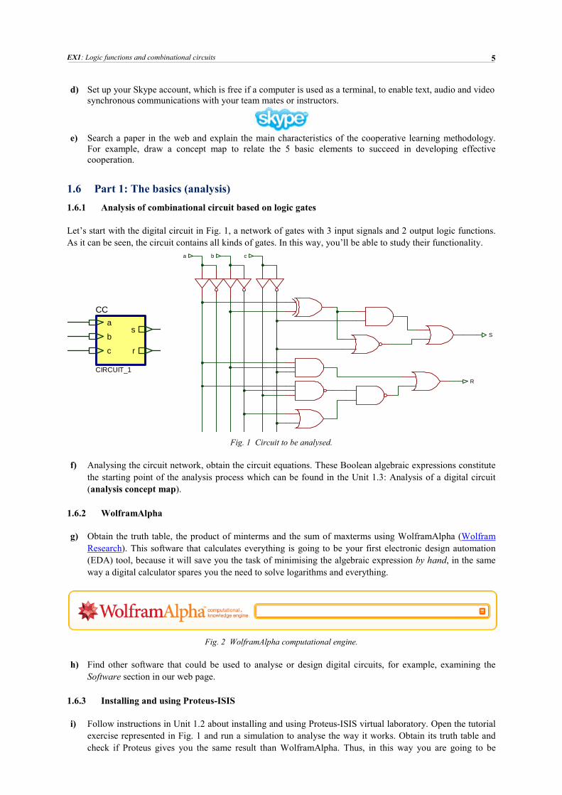
1.6.1 Analysis of combinational circuit based on logic gates
Let’s start with the digital circuit in Fig. 1, a network of gates with 3 input signals and 2 output logic functions. As it can be seen, the circuit contains all kinds of gates. In this way, you’ll be able to study their functionality.
Fig. 1 Circuit to be analysed.
f) Analysing the circuit network, obtain the circuit equations. These Boolean algebraic expressions constitute the starting point of the analysis process which can be found in the Unit 1.3: Analysis of a digital circuit (analysis concept map).
1.6.2 WolframAlpha
g) Obtain the truth table, the product of minterms and the sum of maxterms using WolframAlpha (Wolfram Research). This software that calculates everything is going to be your first electronic design automation (EDA) tool, because it will save you the task of minimising the algebraic expression by hand, in the same way a digital calculator spares you the need to solve logarithms and everything.
Fig. 2 WolframAlpha computational engine.
h) Find other software that could be used to analyse or design digital circuits, for example, examining the Software section in our web page.
1.6.3 Installing and using Proteus-ISIS
i) Follow instructions in Unit 1.2 about installing and using Proteus-ISIS virtual laboratory. Open the tutorial exercise represented in Fig. 1 and run a simulation to analyse the way it works. Obtain its truth table and check if Proteus gives you the same result than WolframAlpha. Thus, in this way you are going to be
CC
CIRCUIT_1
a
b
c
s
r
a b c
S
R

EPSC – E1: Electronics I
6
equipped with two very convenient software tools that will facilitate the design process of digital circuits. In the web pages will see several alternatives to the way of applying input signals, stimulus or test vectors. The idea behind the testing process is to verify all the truth table combinations.
j) Open the tutorial exercise represented in Fig. 1 and run a simulation to analyse the way it works. Obtain its
truth table and check if Proteus gives you the same result than WolframAlpha. Thus, in this way you are going to be equipped with two very convenient software tools that will facilitate the design process of digital circuits. In the web pages will see several alternatives to the way of applying input signals, stimulus or test vectors. Fig. 3 shows an EasyHDL (Proteus scripting language) example, for inputting digital combinations to a circuit. The idea behind the testing process is to verify all the truth table combinations.
*SCRIPT GENERATOR TEST_SIGNALS PIN X[0..2] FLOAT BITTIME = 1000m // Here you are all the truth table. // A binary combination every 1 s X = 000 SLEEP FOR BITTIME X = 001 SLEEP FOR BITTIME X = 010 SLEEP FOR BITTIME X = 011 SLEEP FOR BITTIME X = 100 SLEEP FOR BITTIME X = 101 SLEEP FOR BITTIME X = 110 SLEEP FOR BITTIME X = 111 *ENDSCRIPT
Fig. 3 Example of a Proteus script file automatically to apply all the 8 input combinations to a given circuit.
1.6.4 Installing and using ispLEVER Classic
Follow instruction in Unit 1.4 to install ispLEVER Classic for implementing projects into simple programmable logic devices (sPLD) like the GAL22V10. Check the software by running the following example design, which consist in a mix of schematics and VHDL files.
Basically, only two modules are needed to be installed, the software and the synthesiser Synplify:
• isp7_0m1_classic_ispLEVER.exe (the name will change accordingly to the version) • SYN_p3.exe (Synplify Lattice version is a synthesiser tool from Synopsys)
One student of the group may also install the ispVMSystem in order to program the PROTOGAL board with the sPLD JED configuration file. A universal programmer7 like the TopMax is another alternative (see Fig. 11b). ispLEVER Project Navigator and the GAL22V10 device
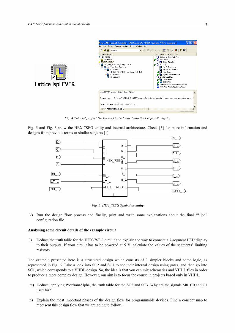
A sample project in a zip file at the E1 web will be provided for checking the correctness of the software installation before attempting any design: a basic HEX-7SEG decoder. This is project of a combinational circuit corresponding to a hexadecimal to 7-segment decoder. It is built using a mix of schematics in the classical way and VHDL modules. Our aim is to synthesise it and generate the configuration JED file prepared to be downloaded into the simple programmable logic device (sPLD) GAL22V10. This is the most elemental sPLD from Lattice and a classic that has become a standard circuit for many years. It has a capacity around 500 gates and also contains 10 D-type flip-flops. Execute “Project Navigator” and load the already defined initial project HEX-7SEG.
7 http://epsc.upc.edu/projectes/ed/Instruments/Instruments.html
EX1: Logic functions and combinational circuits
Fig. 4 Tutorial project HEX
Fig. 5 and Fig. 6 show the HEX-7SEG entity andesigns from previous terms or similar subjects
k) Run the design flow process and finally, print and write some explanations about the final “*.jed” configuration file.
Analysing some circuit details of the example circuit
l) Deduce the truth table for the HEXto their outputs. If your circuit has to be powered at 5 V, calculate the values of the segments’ limiting resistors.
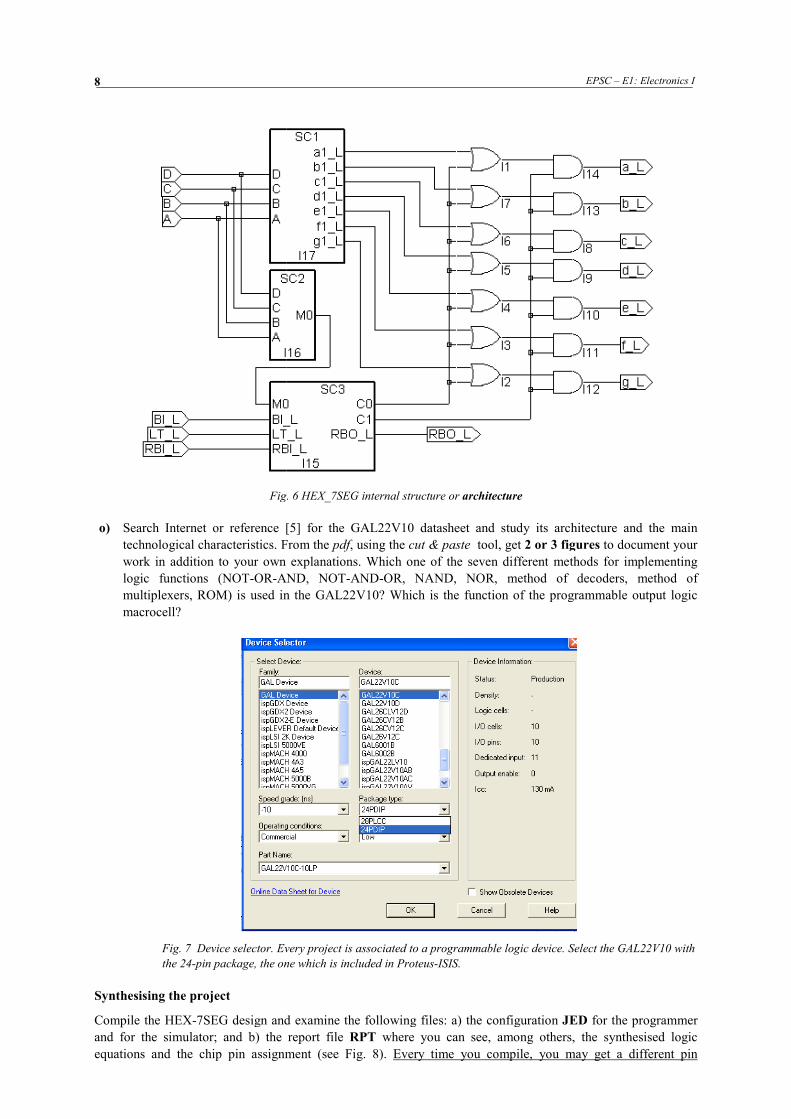
The example presented here is a structured design which consists of 3 simpler blocks and some logic, as represented in Fig. 6. Take a look into SC2 and SC3 to see their internal design using gates, and then go into SC1, which corresponds to a VHDL design. So, theto produce a more complex design. However, our aim is to focus the course in projects based only in VHDL. m) Deduce, applying WorframAlpha, the truth table for the SC2 and SC3. Why are the signals
used for? n) Explain the most important phases of the
represent this design flow that we are going to follow.
Logic functions and combinational circuits
Tutorial project HEX-7SEG to be loaded into the Project Navigator
7SEG entity and internal architecture. Check [3] for more information and designs from previous terms or similar subjects [1].
Fig. 5 HEX_7SEG Symbol or entity
Run the design flow process and finally, print and write some explanations about the final “*.jed”
Analysing some circuit details of the example circuit
Deduce the truth table for the HEX-7SEG circuit and explain the way to connect a 7to their outputs. If your circuit has to be powered at 5 V, calculate the values of the segments’ limiting
The example presented here is a structured design which consists of 3 simpler blocks and some logic, as . Take a look into SC2 and SC3 to see their internal design using gates, and then go into
SC1, which corresponds to a VHDL design. So, the idea is that you can mix schematics and VHDL files in order to produce a more complex design. However, our aim is to focus the course in projects based only in VHDL.
Deduce, applying WorframAlpha, the truth table for the SC2 and SC3. Why are the signals
Explain the most important phases of the design flow for programmable devices. Find a concept map to represent this design flow that we are going to follow.
7
7SEG to be loaded into the Project Navigator
for more information and
Run the design flow process and finally, print and write some explanations about the final “*.jed”
a 7-segment LED display to their outputs. If your circuit has to be powered at 5 V, calculate the values of the segments’ limiting
The example presented here is a structured design which consists of 3 simpler blocks and some logic, as . Take a look into SC2 and SC3 to see their internal design using gates, and then go into
idea is that you can mix schematics and VHDL files in order to produce a more complex design. However, our aim is to focus the course in projects based only in VHDL.
Deduce, applying WorframAlpha, the truth table for the SC2 and SC3. Why are the signals M0, C0 and C1
for programmable devices. Find a concept map to
8
Fig.
o) Search Internet or reference [5]technological characteristics. From the work in addition to your own explanations. Which one of the logic functions (NOT-OR-AND, NOTmultiplexers, ROM) is used in the GAL22V10? Which is the function of the programmable omacrocell?
Fig. 7 Device selector. Every project is associated to a programmable logic device. Select the GAL22V10 with
the 24-pin package, the one which is included in Proteus
Synthesising the project
Compile the HEX-7SEG design and examine the following files: a) the configuration and for the simulator; and b) the report file equations and the chip pin assignment (see
Fig. 6 HEX_7SEG internal structure or architecture
[5] for the GAL22V10 datasheet and study its architecture and the main technological characteristics. From the pdf, using the cut & paste tool, get 2 or 3 figures
on to your own explanations. Which one of the seven different methods for implementing AND, NOT-AND-OR, NAND, NOR, method of decoders, method of
is used in the GAL22V10? Which is the function of the programmable o
. Every project is associated to a programmable logic device. Select the GAL22V10 with
pin package, the one which is included in Proteus-ISIS.
7SEG design and examine the following files: a) the configuration JEDand for the simulator; and b) the report file RPT where you can see, among others, the synthesised logic equations and the chip pin assignment (see Fig. 8). Every time you compile, you may get a different pin
EPSC – E1: Electronics I
and study its architecture and the main 2 or 3 figures to document your
different methods for implementing OR, NAND, NOR, method of decoders, method of
is used in the GAL22V10? Which is the function of the programmable output logic
. Every project is associated to a programmable logic device. Select the GAL22V10 with
JED for the programmer where you can see, among others, the synthesised logic
Every time you compile, you may get a different pin
EX1: Logic functions and combinational circuits
9
assignment distribution, especially if the VHDL source files are modified. This problem is solved in the case of CPLD and FPGA devices using a constrain file (or a pin-assignment tool) specifying at which pins do you want to connect the entity ports while synthesising.
Fig. 8 Pin assignment as seen in the report output file (RPT)
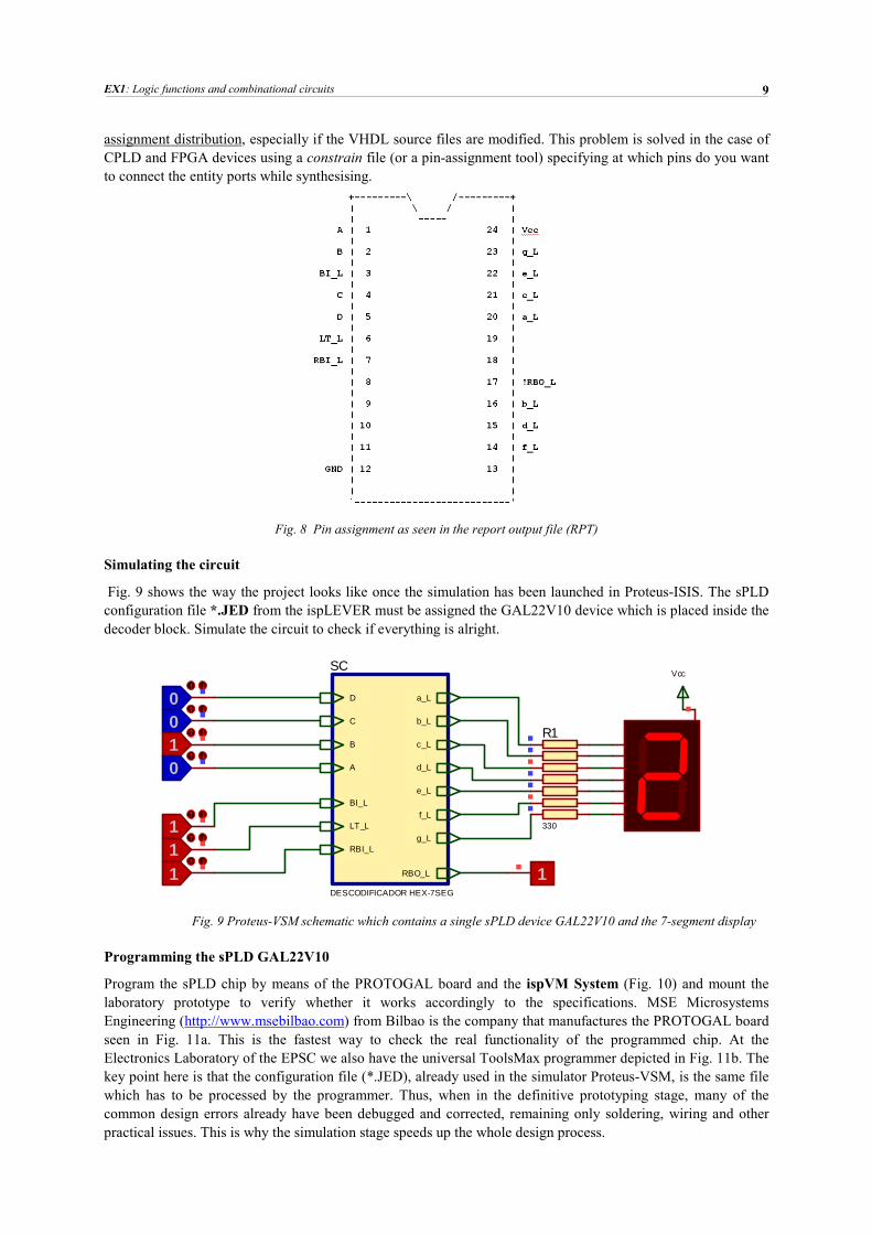
Simulating the circuit
Fig. 9 shows the way the project looks like once the simulation has been launched in Proteus-ISIS. The sPLD configuration file *.JED from the ispLEVER must be assigned the GAL22V10 device which is placed inside the decoder block. Simulate the circuit to check if everything is alright.
Fig. 9 Proteus-VSM schematic which contains a single sPLD device GAL22V10 and the 7-segment display
Programming the sPLD GAL22V10
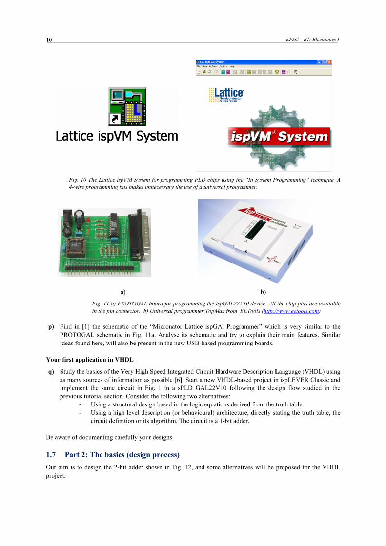
Program the sPLD chip by means of the PROTOGAL board and the ispVM System (Fig. 10) and mount the laboratory prototype to verify whether it works accordingly to the specifications. MSE Microsystems Engineering (http://www.msebilbao.com) from Bilbao is the company that manufactures the PROTOGAL board seen in Fig. 11a. This is the fastest way to check the real functionality of the programmed chip. At the Electronics Laboratory of the EPSC we also have the universal ToolsMax programmer depicted in Fig. 11b. The key point here is that the configuration file (*.JED), already used in the simulator Proteus-VSM, is the same file which has to be processed by the programmer. Thus, when in the definitive prototyping stage, many of the common design errors already have been debugged and corrected, remaining only soldering, wiring and other practical issues. This is why the simulation stage speeds up the whole design process.
SC
DESCODIFICADOR HEX-7SEG
B
A
b_L
c_L
d_L
e_L
f_L
g_L
a_LD
C
RBO_L
LT_L
BI_L
RBI_L
R1
330
Vcc
0010
111 1
EPSC – E1: Electronics I
10
Fig. 10 The Lattice ispVM System for programming PLD chips using the “In System Programming” technique. A
4-wire programming bus makes unnecessary the use of a universal programmer.
a) b)
Fig. 11 a) PROTOGAL board for programming the ispGAL22V10 device. All the chip pins are available
in the pin connector. b) Universal programmer TopMax from EETools (http://www.eetools.com)
p) Find in [1] the schematic of the “Micronator Lattice ispGAl Programmer” which is very similar to the PROTOGAL schematic in Fig. 11a. Analyse its schematic and try to explain their main features. Similar ideas found here, will also be present in the new USB-based programming boards.
Your first application in VHDL
q) Study the basics of the Very High Speed Integrated Circuit Hardware Description Language (VHDL) using as many sources of information as possible [6]. Start a new VHDL-based project in ispLEVER Classic and implement the same circuit in Fig. 1 in a sPLD GAL22V10 following the design flow studied in the previous tutorial section. Consider the following two alternatives:
- Using a structural design based in the logic equations derived from the truth table. - Using a high level description (or behavioural) architecture, directly stating the truth table, the
circuit definition or its algorithm. The circuit is a 1-bit adder. Be aware of documenting carefully your designs.
1.7 Part 2: The basics (design process)
Our aim is to design the 2-bit adder shown in Fig. 12, and some alternatives will be proposed for the VHDL project.

EX1: Logic functions and combinational circuits
11
Fig. 12 A 2-bit expandable adder
1.7.1 Truth table, sum of minterms and product of maxterms
r) Construct the truth table for the circuit. Write the equations for the: - Sum of minterms - Product of maxterms
1.7.2 Simplifying logic functions using Minilog
s) Install Minilog in your computer, and simplify the truth table to obtain the logic equations for the: - Sum of products - Product of sums
1.7.3 Circuits in CMOS technology
t) Draw a circuit in Proteus-ISIS using only NAND from CMOS technology and verify it. 1.7.4 Circuits in LS-TTL technology
u) Draw a circuit in Proteus-ISIS using only NOR from LS-TTL technology and verify it. 1.7.5 Flat design in VHDL
v) Make a new project using a single VHDL file (flat design, thus considering it as a small circuit) which will have the functionality of the entity in Fig. 12. Implement the circuit into a sPLD and verify it in Proteus ISIS.
- Using a structural design based in the logic equations (minimised or not) derived from the truth table.
- Using a high level description (the truth table itself) for the 2-bit adder entity. 1.7.6 Hierarchical design in VHDL
w) Make a new project consisting in many VHDL files (hierarchical design with instantiated components interconnected by signals) which will have the functionality of the entity in Fig. 12. Implement the circuit into a sPLD and verify it in Proteus-ISIS.
- Firstly, produce the component SUM1 as a flat design and simulate it. - And secondly, use it as a building block for the hierarchical design. Use a buffer for every input
and output in the circuit. Your project probably will consist of two VHDL files: the entity top design with instantiated components, and the file for the SUM1 component.
1.8 Part 3: Building a library of standard combinational circuits
Our aim is to start a library of components which are going to be implemented following different styles, like in the previous example of the 2-bit adder. Here you are different alternatives to the design that can be taken into account when designing combinational circuits:
ADDER2
CIRCUIT_2
Ci
A0
A1
S0
S1
B0
B1Co

EPSC – E1: Electronics I
12
- BUFFER/NOT – AND – OR - BUFFER/NOT – OR– AND - Only NOR - Only NAND - Flat design or a single structure - Hierarchical design, chaining elemental blocks of the same kind among other components or
logic. - Only VHDL based projects - CMOS technology schematics - LS-TTL8 technology schematics - Using classic commercial chips in CMOS or LS-TTL
x) Select a component from the following list and find a HADES java script to analyse the way it works. Such
analysis implies drawing its symbol, writing its truth table and important equations. Every cooperative group have to choose a different device:
- Decoder DEC4:16 with enable - A 16-channel data multiplexer MUX16 with enable - Encoder for 10 keys ENC10:4 with key pressed signal - A cascadable 4-bit comparator COMP4 (A<B, A=B, A>B) - Hexadecimal to 7- segment decoder HEX-7SEG with blanking input and ripple blanking input
and output (to blank leading zeroes in a chain). - A quadruple data multiplexer of 4 channels 4MUX4
y) Select a component from the previous list and implement it in both versions: 1) using gates, and 2) using
VHDL. Every cooperative group have to choose a different device and attempt different approaches:
1.9 Another design example
z) The idea: a combinational circuit to count the number of cars parked in a park of 40 slots. When a particular slot is occupied, its ultrasonic sensor provides a ‘1’ signal, and a ‘0’ otherwise. A car park full signal is also provided when all slots are occupied. This project is essentially, a ones counter, a device to count de number of ‘1’ in any position. Solve the problem as a VHDL project implemented in sPLD chips using a hierarchical structure of elemental components. The final circuit, which has to be verified in Proteus-ISIS, has to contain only GAL22V10 chips and the digits to show the parking car count. A hint: start the problem solving a parking slot counter for only 4 cars.
8 The only reason for using these obsolete technologies is because the simulation models for all the devices and chips are available in Proteus.
Do not modify the text from page 3 to page 12

EX1: Logic functions and combinational circuits
13
1.10 Problem solution (títol 2)
1.10.1 Part 1 (títol 3)
Part 1.1 (títol 4)
És necessari que seguiu aquestes indicacions per qualsevol dels vostres documents en aquesta assignatura. Aprendre-les forma part de la competència de comunicació escrita. Adapteu els vostres documents al format subministrat per aquesta plantilla.
� Si alguna indicació o format no l’acabeu d’entendre bé, pregunteu-nos-ho o aclariu els dubtes, però no lliureu mai res que no compleixi aquestes indicacions perquè no us ho corregirem i perdreu el temps.
Afegiu aquí el vostre text (estil normal) encapçalat amb títols (Títol 2 i 3 i 4), amb figures (estil “llegenda” o “epígrafe”) i referències creuades en el text com aquesta Fig. 13 (és una referència creuada a la llegenda, veureu que surt en color gris quan la cliqueu) a les figures que inseriu. Fixeu-vos que la primera vegada que obrireu aquest document en Word 2007, no us sortirà aquesta llegenda “Fig.”, així que haureu de crear-ne una, i després, encara que la esborreu,ja us quedarà la referència. Veureu també que la numeració de les figures és un paràmetre automàtic. Si seleccioneu tot el document, i premeu “F9” actualitzareu tota la numeració. També l’índex de la pag. 2 és completament automàtic. Es genera sol ( a partir de � referències, índex de continguts, Inseriu un índex de continguts) i s’actualitza sol a partir també de “F9” havent seleccionat tot el text de document. És possible que la primera vegada que l’actualitzeu desaparegui. No passa res, simplement cal tornar-lo a generar a partir del menú referències i taula de contingut. Fixeu-vos en la Fig. 13. Les imatges han d’estar centrades i alineades amb el text. Si voleu posar un parell d’imatges a la mateixa línia, inseriu primer una taula d’un parell de columnes i tot seguit feu invisibles les vores. El millor que podeu fer és “cut & paste” de la pròpia taula que veieu, i, canviar les figures per les vostres. Feu referència també en el text a les fonts bibliogràfiques o de web que consulteu d’aquesta manera [1] (és una referència creuada a l’element numerat [1]). Expliqueu perquè les heu consultat i quina informació útil heu trobat. Per corregir la primera versió del vostre treball, no imprimiu ni lliureu des de les pàgines 3 a la 12. És l’enunciat del problema. Sols cal que imprimiu les 2 primeres pàgines que contenen els detalls personals, el resum i l’índex, i a partir d’aquesta mateixa pàgina 13. Però feu-ho amb la numeració correcta. És a dir, treballeu sempre sobre aquest document, i en tot cas, importeu altres textos que tingueu cap a aquest mateix document i formateu-los correctament.
� Insistim sobre això mateix: treballeu sempre sobre aquest mateix fitxer per preparar la vostra solució. Així usareu tots els estils i formats que ja té predefinits aquest document.

EPSC – E1: Electronics I
14
Fig. 13 Exemple de peu de figura que segueix la numeració de l’enunciat (llegenda).
Heu d’instal·lar els correctors ortogràfics en català, espanyol i anglès en el vostre paquet d’eines office. I sobretot, corregir qualsevol error mentre escriviu. Si treballeu això estalviareu molta feina als vostres companys i instructors.
1.11 References
Modify or add new references to this section. Follow the same format. [1] http://epsc.upc.edu/projectes/ed/. Comment: Course wed page where to find a lot of resources for the course.
Specially, materials from previous editions. Read the section on theory about digital systems. [visited 12/2009]
[2] Brown,S., Vranesic, Z., “Fundamentals of digital logic with VHDL design”, McGraw-Hill, 2005. Comment:
The Figure 1.7 contains an example of a design flow for logic circuits and Figure 2.29 the structure of a typical CAD/EDA system.
[3] http://epsc.upc.edu/projectes/ed/ED/problemes/problemes_PA/Problemes_PA.htm. Comment: Web page
where an example of a hexadecimal to seven-segment decoder (HEX-7SEG) is explained. [Visited 12/2009] [4] http://epsc.upc.edu/projectes/ed/SED/projectes_aplicacio/projectSED.html. Comment: Web page where to
find a template on distributing tasks among the members of a cooperative team. [Visited 12/2009].
[5] Unit 1.5: Simple programmable logic devices (PLD).
[6] Unit 1.6: Very High Speed Integrated Circuit Hardware description language (VHDL).

EX1: Logic functions and combinational circuits
15
1.12 Study plan to solve the exercise
Check the documentation in our web [4], to look at ways to establish a study plan, a task distribution scheme and other requirements to succeed in producing a good solution when working cooperatively: flux diagrams, concept maps, schematics, tables, pictures, etc. (This section is mandatory. It must be filled in order to get a mark.)

EPSC – E1: Electronics I
16
1.13 Topics and activities checklist
Topics Activities
Group member in
charge Comments
1 2 3 1. Use your official UPC e-mail address 2. Use and manage an e-mail client like
Thunderbird or Outlook. 3. Use a SFTP client like WinSCP to access
your network disk drive “L”.
a), b), c), d)
4. Explain the five elements to achieve effective cooperative learning.
e)
5. Explain the concept of a top-down design of a digital circuit.
f)
6. Explain the logic gates AND, NAND, OR, NOR, XOR, NXOR, NOT)
f)
7. Analyze a logic circuit built using logic gates. Analysis concept map.
f)
8. Use WolframAlpha to obtain a circuit’s truth table.
f)g), m)
9. Use the HADES JAVA-based platform simulate. h) 10. Simulate a digital circuit in Proteus-ISIS. i) 11. Install the ispLEVER Classic and follow its
design flow to implement an example project into a sPLD.
j), k)
12. Search books and the Internet to learn about VHDL language.
q)
13. Explain the VDHL-based design flow of a modern digital circuit.
q)
14. Explain the basics of a SPLD GAL22V10. o), p) 15. Structural versus behavioural design styles in
VHDL q)
16. Relate the following concepts for designing a logic circuit: truth table, Boolean algebra and logic functions, minimisation, SoP (sum of products) and PoS (product of sums), canonical algebraic equations, minterms and maxterms. Design concept map.
r), s)
17. Simplify or minimize logic function using software like Minilog.exe.
s)
18. Find the datasheets of SSI and MSI chips. t), u) 19. Explain the concepts of flat and hierarchical
designs using components and their instantiation in VHDL language.
w)
20. Design and use standard blocks and apply combinational circuits.
x), y), z)
21. Produce a concept map (or a mind map) to explain a topic on the subject.List advantages of using VHDL
q)
22. Organise a plan to work in cooperative group for solving the exercises.
Sec. 1.12
23. Analyse your own individual and group study time.
Sec. 1.12
24. Produce a quality written solution using a word processor template:
a. spelling and grammar b. chapter enumeration
Sec. 1.10, 1.11

EX1: Logic functions and combinational circuits
17
c. page headers and footers d. hyperlinks e. cross-references f. figure captions g. text styles for technical reports
25. Assessing Sec. 1.13, 1.14 and
1.15
1.14 Grading grid
Here you are the way the exercise could be grades. Part 1 Part 2 Part 3
Total
Sections Sections Sections Scores 2p 3p 5p Self-assessment Instructor’s grades
1.15 Questions in solving EX19
Write here your questions, comments, doubts, opinions, etc. ...
9 Add more sheets if necessary to report your progress or comments though the exercise.
Aquests fulls de dubtes i d’explicació de com heu anat fent l’exercici són obligatoris. Si no és present, no es corregeix l’exercici i s’ha de tornar a lliurar. Abans de corregir i posar-vos qualificacions volem saber quin ha estat procés en què heu dissenyat els circuits i comparar-lo amb les nostres pròpies observacions de classe.