EVAL-M1-2ED2106S User Manual · 2020-02-14 · M M1 Interface AUX Power Supply PWM VCC Current...
29
Revision 1.0 User Manual www.infineon.com/gatedriver page 1 of 29 2019-09-18 AN2019-19 EVAL-M1-2ED2106S User Manual EVAL-M1-2ED2106S User Manual 2ED2106S06F Evaluation board for BLDC motor drives About this document Scope and purpose This application note provides an overview of the evaluation board EVAL-M1-2ED2106S concerning its main features, hardware description, thermal performance and typical waveforms, etc. The EVAL-M1-2ED2106S board is a power drive board including driver ICs, IGBTs, a power connector and signal interface. The board is intended to drive a brushless direct current (BLDC) motor by connecting to an external controller board such as EVAL-M1-101T. The board aims to boost Infineon’s newly promoted 650 V high and low side gate driver 2ED2106S06F using the silicon-on-isolator (SOI) technology. Intended audience This application note is intended for all technical specialists likely to evaluate the 650 V SOI gate drivers for general applications. Table of contents About this document ....................................................................................................................... 1 Table of contents ............................................................................................................................ 1 1 Safety precautions ................................................................................................................. 2 2 Introduction .......................................................................................................................... 3 3 Main features of EVAL-M1-2ED2106S ........................................................................................ 4 3.1 Board specifications of EVAL-M1-2ED2106S........................................................................................... 4 3.2 Pin assignment ........................................................................................................................................ 6 4 Key components in the EVAL-M1-2ED2106S ............................................................................... 8 4.1 650 V SOI gate driver ............................................................................................................................... 8 4.2 TrenchStop TM IGBT6 IKB10N65ET6 ......................................................................................................... 9 5 Test result of the EVAL-M1-2ED2106S driving BLDC motor ......................................................... 10 5.1 System setup ......................................................................................................................................... 10 5.2 Waveforms ............................................................................................................................................. 11 6 Thermal analysis of the EVAL-M1-2ED2106S ............................................................................. 13 7 Circuit diagram of the EVAL-M1-2ED2106S ............................................................................... 14 7.1 Schematic overview .............................................................................................................................. 14 7.2 Main power circuit ................................................................................................................................. 15 7.3 OCP circuit ............................................................................................................................................. 15 7.4 Auxiliary power supply circuit............................................................................................................... 18 8 PCB layout of the EVAL-M1-2ED2106S ...................................................................................... 19 9 Bill of material ...................................................................................................................... 24 10 Reference ............................................................................................................................. 27 Revision history............................................................................................................................. 28
Transcript of EVAL-M1-2ED2106S User Manual · 2020-02-14 · M M1 Interface AUX Power Supply PWM VCC Current...

Revision 1.0 User Manual
www.infineon.com/gatedriver page 1 of 29 2019-09-18
AN2019-19 EVAL-M1-2ED2106S User Manual
EVAL-M1-2ED2106S User Manual
2ED2106S06F Evaluation board for BLDC motor drives
About this document
Scope and purpose
This application note provides an overview of the evaluation board EVAL-M1-2ED2106S concerning its main
features, hardware description, thermal performance and typical waveforms, etc.
The EVAL-M1-2ED2106S board is a power drive board including driver ICs, IGBTs, a power connector and signal
interface. The board is intended to drive a brushless direct current (BLDC) motor by connecting to an external
controller board such as EVAL-M1-101T.
The board aims to boost Infineon’s newly promoted 650 V high and low side gate driver 2ED2106S06F using
the silicon-on-isolator (SOI) technology.
Intended audience
This application note is intended for all technical specialists likely to evaluate the 650 V SOI gate drivers for
general applications.
Table of contents
About this document ....................................................................................................................... 1
Table of contents ............................................................................................................................ 1
1 Safety precautions ................................................................................................................. 2
2 Introduction .......................................................................................................................... 3
3 Main features of EVAL-M1-2ED2106S ........................................................................................ 4
3.1 Board specifications of EVAL-M1-2ED2106S ........................................................................................... 4
3.2 Pin assignment ........................................................................................................................................ 6
4 Key components in the EVAL-M1-2ED2106S ............................................................................... 8
4.1 650 V SOI gate driver ............................................................................................................................... 8
4.2 TrenchStopTM IGBT6 IKB10N65ET6 ......................................................................................................... 9
5 Test result of the EVAL-M1-2ED2106S driving BLDC motor ......................................................... 10
5.1 System setup ......................................................................................................................................... 10
5.2 Waveforms ............................................................................................................................................. 11
6 Thermal analysis of the EVAL-M1-2ED2106S ............................................................................. 13
7 Circuit diagram of the EVAL-M1-2ED2106S ............................................................................... 14
7.1 Schematic overview .............................................................................................................................. 14
7.2 Main power circuit ................................................................................................................................. 15
7.3 OCP circuit ............................................................................................................................................. 15
7.4 Auxiliary power supply circuit ............................................................................................................... 18
8 PCB layout of the EVAL-M1-2ED2106S ...................................................................................... 19
9 Bill of material ...................................................................................................................... 24
10 Reference ............................................................................................................................. 27
Revision history............................................................................................................................. 28

User Manual 2 of 29 Revision 1.0
2019-09-18
EVAL-M1-2ED2106S User Manual 2ED2106S06F drive board for BLDC motor
Safety precautions
1 Safety precautions
Please read carefully the following statements in Table 1 regarding hazards associated with the evaluation
board and the testing system, and the safety precautions listed in the manual.
Table 1 Safety precautions
Caution: The ground potential of the EVAL-M1-2ED2106S board is biased to a negative
DC bus voltage potential. When measuring voltage waveform by oscilloscope, the
ground of the device needs to be isolated. Failure to do so may result in personal injury
or death, and equipment damage.
Caution: Only personnel familiar with the drive and associated machinery should plan
or implement the installation, start-up and subsequent maintenance of the system.
Failure to comply may result in personal injury and/or equipment damage.
Caution: The surfaces of the drive may become hot, which may cause injury.
Caution: The EVAL-M1-2ED2106S board contains parts and assemblies sensitive to
electrostatic discharge (ESD). Electrostatic control precautions are required when
installing, testing, servicing or repairing this assembly. Component damage may result
if ESD control procedures are not followed. If you are not familiar with electrostatic
control procedures, refer to applicable ESD protection handbooks and guidelines.
Caution: An incorrectly applied or installed drive can result in component damage or
reduction in product lifetime. Wiring or application errors such as undersized motor,
incorrect or inadequate DC supply, or excessive ambient temperatures may result in
system malfunction.
Caution: Remove or connect the control board from, or to, the power drive. Wait three
minutes after removing power from the power drive to discharge the bus capacitors. Do
not attempt to service the drive until the bus capacitors have discharged to zero. Failure
to do so may result in personal injury or death.

User Manual 3 of 29 Revision 1.0
2019-09-18
EVAL-M1-2ED2106S User Manual 2ED2106S06F drive board for BLDC motor
Introduction
2 Introduction
Note: Evaluation boards are not subject to the same procedures as regular products regarding Returned
Material Analysis (RMA), Process Change Notification (PCN) and Product Discontinuation (PD).
Evaluation boards are intended to be used under laboratory conditions and by trained specialists
only.
The power stage of the evaluation board EVAL-M1-2ED2106S consists of a three-phase inverter with a single-
shunt configuration, which is widely used for the BLDC motor drive in home appliances.
The 650 V SOI gate driver 2ED2106S06F is highlighted in the board. Different from traditional drivers with
junction isolated (JI) technology, the SOI gate driver shows the benefits of a simpler design by integrating the
boot strap diode, and there is higher tolerance of the negative VS due to the SOI technology inherently.
The IGBTs with Infineon TrenchStopTM IGBT6 technology have been adopted in the board. Thanks to the high
performance of the IGBT6 with the optimized conduction loss and switching loss, under natural cooling the
board can run up to 300 W, which is common for refrigerator products.
The board is intended to work together with the controller board EVAL-M1-101T to deliver a total Infineon
solution with low cost and high robustness for the home appliance applications.
The board is available via regular Infineon distribution partners as well as on Infineon's website. The features of
this board are described in Chapter 3 of this document. The remaining sections provide information to enable
customers to copy, modify and qualify the design for production according to their own specific requirements.
Environmental conditions were considered in the design of the EVAL-M1-2ED2106S. However, the board has
not been qualified in terms of safety requirements, manufacturing and operation over the entire operating
temperature range or lifetime. The boards provided by Infineon are subject to functional testing only.
Figure 1 depicts the block diagram of the EVAL-M1-2ED2106S.
SOIGate
Driver
SOIGate
Driver
SOIGate
Driver
M
M1 Interface
AUXPowerSupply
PWM
VCC
CurrentSensing
Cbus
EVAL-M1-2ED2106S
Figure 1 Block diagram of the EVAL-M1-2ED2106S

User Manual 4 of 29 Revision 1.0
2019-09-18
EVAL-M1-2ED2106S User Manual 2ED2106S06F drive board for BLDC motor
Main features of EVAL-M1-2ED2106S
3 Main features of EVAL-M1-2ED2106S
The main features of the evaluation board EVAL-M1-2ED2106S include:
• Three-phase inverter with single-shunt configuration, suitable for home appliance applications
• DC voltage input that can come directly from the rectified DC voltage of single-phase 230 VAC input
• 650 V SOI gate driver 2ED2106S06F with large negative VS tolerance
• 10 A/650 V rated IGBT6 IKB10N65ET6 with a better thermal performance
• The board can run a BLDC motor by connecting to an external control board EVAL-M1-101T
• Auxiliary power supply is included in the board
• Natural cooling with a heatsink is installed on bottom side
3.1 Board specifications of EVAL-M1-2ED2106S
The detailed specifications of the EVAL-M1-2ED2106S are described in Table 2.
Table 2 EVAL-M1-2ED2106S board specifications
Parameters Typical maximum Conditions / comments
Input
Voltage (VDC) 310 380 DC+ to GND
Current ( ARMS) 0.97 310 VDC input, 300 W input power
Output
Phase current ( ARMS) 1.6 310 VDC input, 300 W input power
Switching frequency
Inverter frequency (kHz) 15
Current feedback
Current sampling shunt 100 mΩ single-shunt configuration
Aux power supply
Supply voltage ( VCC) 15 on-board aux power supply
System environment
Ambient temperature 0~50 ℃ natural ventilation, maximum RH of 95 %
PCB characteristics
Dimensions Length*Width=126x84 mm2, 2 layers, PCB thickness=1.6 mm,
copper thickness=1 oZ
Material FR-4, RoHS-compliant
User Manual 5 of 29 Revision 1.0
2019-09-18
EVAL-M1-2ED2106S User Manual 2ED2106S06F drive board for BLDC motor
Main features of EVAL-M1-2ED2106S
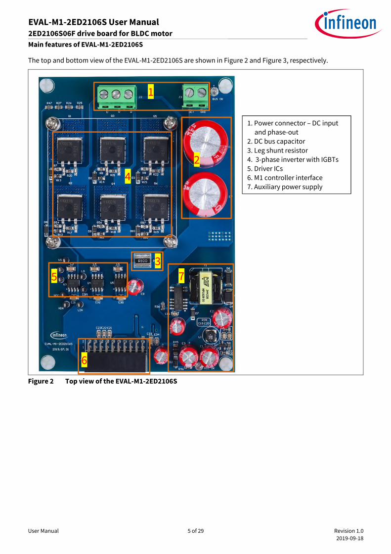
The top and bottom view of the EVAL-M1-2ED2106S are shown in Figure 2 and Figure 3, respectively.
Figure 2 Top view of the EVAL-M1-2ED2106S
1. Power connector – DC input
and phase-out
2. DC bus capacitor
3. Leg shunt resistor
4. 3-phase inverter with IGBTs
5. Driver ICs
6. M1 controller interface
7. Auxiliary power supply
1
2
3
4
5
6
7

User Manual 6 of 29 Revision 1.0
2019-09-18
EVAL-M1-2ED2106S User Manual 2ED2106S06F drive board for BLDC motor
Main features of EVAL-M1-2ED2106S
Figure 3 Bottom view of the EVAL-M1-2ED2106S
3.2 Pin assignment
The pin assignment of the phase-out connector and DC input connector are listed in Table 3 and Table 4,
respectively. The pin names are also marked on the PCB.
Table 3 J2 – Phase-out connector
S. No. Pin name Details
U U – Phase-out wiring terminal
V V – Phase-out wiring terminal
W W – Phase-out wiring terminal
8. Heatsink installed on the back
side
9. OCP circuit
8
9

User Manual 7 of 29 Revision 1.0
2019-09-18
EVAL-M1-2ED2106S User Manual 2ED2106S06F drive board for BLDC motor
Main features of EVAL-M1-2ED2106S
Table 4 J3 – DC input connector
S. No. Pin name Details
DC+ DC bus positive input
GND DC bus return
The controller interface is M1 that pin-to-pin matches with the EVAL-M1-101T. The pin assignment is listed in
Table 5.
Table 5 CN2 – Controller interface
S. No. Pin name Details
1 UH U-phase high side PWM input
2 GND signal reference ground
3 UL U-phase low side PWM input
4 GND signal reference ground
5 VH V-phase high side PWM input
6 +3.3 V +3.3 V power supply
7 VL V-phase low side PWM input
8 +3.3 V +3.3 V power supply
9 WH W-phase high side PWM input
10 I_U+ positive of the single-shunt current sensing
11 WL W-phase low side PWM input
12 I_U- negative of the single-shunt current sensing
13 GK Gate kill signal output
14 DCB DC bus voltage sensing output
15 NC
Not connected
16 NC
17 NC
18 NC
19 NC
20 VCC VCC (+15 V) to the controller board
User Manual 8 of 29 Revision 1.0
2019-09-18
EVAL-M1-2ED2106S User Manual 2ED2106S06F drive board for BLDC motor
Key components in the EVAL-M1-2ED2106S
4 Key components in the EVAL-M1-2ED2106S
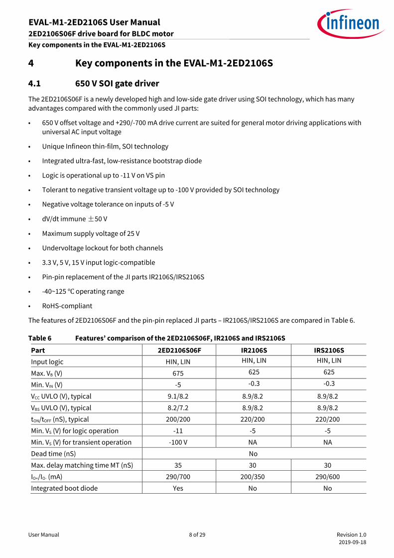
4.1 650 V SOI gate driver
The 2ED2106S06F is a newly developed high and low-side gate driver using SOI technology, which has many
advantages compared with the commonly used JI parts:
• 650 V offset voltage and +290/-700 mA drive current are suited for general motor driving applications with
universal AC input voltage
• Unique Infineon thin-film, SOI technology
• Integrated ultra-fast, low-resistance bootstrap diode
• Logic is operational up to -11 V on VS pin
• Tolerant to negative transient voltage up to -100 V provided by SOI technology
• Negative voltage tolerance on inputs of -5 V
• dV/dt immune ±50 V
• Maximum supply voltage of 25 V
• Undervoltage lockout for both channels
• 3.3 V, 5 V, 15 V input logic-compatible
• Pin-pin replacement of the JI parts IR2106S/IRS2106S
• -40~125 ℃ operating range
• RoHS-compliant
The features of 2ED2106S06F and the pin-pin replaced JI parts – IR2106S/IRS2106S are compared in Table 6.
Table 6 Features’ comparison of the 2ED2106S06F, IR2106S and IRS2106S
Part 2ED2106S06F IR2106S IRS2106S
Input logic HIN, LIN HIN, LIN HIN, LIN
Max. VB (V) 675 625 625
Min. VIN (V) -5 -0.3 -0.3
VCC UVLO (V), typical 9.1/8.2 8.9/8.2 8.9/8.2
VBS UVLO (V), typical 8.2/7.2 8.9/8.2 8.9/8.2
tON/tOFF (nS), typical 200/200 220/200 220/200
Min. VS (V) for logic operation -11 -5 -5
Min. VS (V) for transient operation -100 V NA NA
Dead time (nS) No
Max. delay matching time MT (nS) 35 30 30
IO+/IO- (mA) 290/700 200/350 290/600
Integrated boot diode Yes No No

User Manual 9 of 29 Revision 1.0
2019-09-18
EVAL-M1-2ED2106S User Manual 2ED2106S06F drive board for BLDC motor
Key components in the EVAL-M1-2ED2106S
4.2 TrenchStopTM IGBT6 IKB10N65ET6
• N-channel
• VCE=650 V, IC=16 A @ 100 ℃
• D2PAK package
• Low VCE(sat) = 1.5 V @ 8.5 A
• Optimized the gate charge QG for smaller switching loss
• 3 uS short-circuit capabiity
• Max 175 ℃ junction temperature
• RoHS-compliant and halogen-free

User Manual 10 of 29 Revision 1.0
2019-09-18
EVAL-M1-2ED2106S User Manual 2ED2106S06F drive board for BLDC motor
Test result of the EVAL-M1-2ED2106S driving BLDC motor
5 Test result of the EVAL-M1-2ED2106S driving BLDC motor
5.1 System setup
The board can run a BLDC motor by connecting to an external controller board. The system setup is shown in
Figure 4. The following notes should be taken into consideration:
• The input voltage should be from a DC source or rectified DC voltage from a 230 VAC source. In the test
herein, a 310 VDC / 1.5 A DC source is used.
Note: there should be a protection circuit containing the NTC and fuse to limit the inrush current during the
power ON.
• A high voltage BLDC motor could run with up to 300 W load. A GK6040-6AC31-WE motor is used here for
test purposes only.
• The VB, HO and VS should be measured by high-voltage, isolated differential probes, whereas the HIN, LIN,
VCC and LO should be measured by low-voltage differential probes.
Figure 4 Test setup for running a BLDC motor
BLDC windings
DC input
Match with the
EVAL-M1-101T

User Manual 11 of 29 Revision 1.0
2019-09-18
EVAL-M1-2ED2106S User Manual 2ED2106S06F drive board for BLDC motor
Test result of the EVAL-M1-2ED2106S driving BLDC motor
5.2 Waveforms
Before running the motor, please double check:
• Correct wiring before powering on the DC+ and GND
• The correct selection and scaling of probes
• The LED named ‘BUS OK’ lights up to indicate a successful DC bus power-up
• The LED named ‘VCC OK’ lights up to indicate a successful +15 V auxiliary power supply
When running the system at 310 VDC input voltage and up to 300 W input power, the typical waveforms are
depicted in Figure 5 and Figure 6.
Figure 5 Test result – PWM input and gate drive output
CH1 – U phase-out current
CH2 – Low side IGBT VGE
CH3 – High side IGBT VGE
CH4 – High side PWM input
User Manual 12 of 29 Revision 1.0
2019-09-18
EVAL-M1-2ED2106S User Manual 2ED2106S06F drive board for BLDC motor
Test result of the EVAL-M1-2ED2106S driving BLDC motor
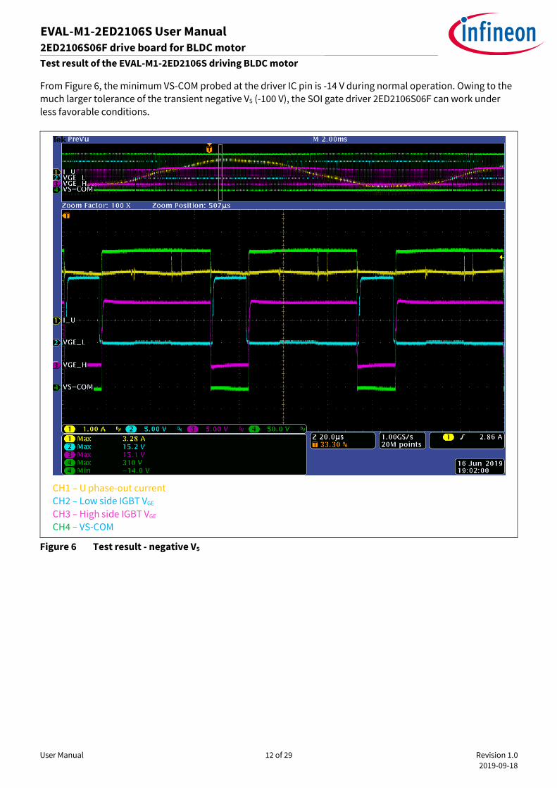
From Figure 6, the minimum VS-COM probed at the driver IC pin is -14 V during normal operation. Owing to the
much larger tolerance of the transient negative VS (-100 V), the SOI gate driver 2ED2106S06F can work under
less favorable conditions.
Figure 6 Test result - negative VS
CH1 – U phase-out current
CH2 – Low side IGBT VGE
CH3 – High side IGBT VGE
CH4 – VS-COM

User Manual 13 of 29 Revision 1.0
2019-09-18
EVAL-M1-2ED2106S User Manual 2ED2106S06F drive board for BLDC motor
Thermal analysis of the EVAL-M1-2ED2106S
6 Thermal analysis of the EVAL-M1-2ED2106S
The thermal performance is evaluated at 310 VDC input voltage and 300 W input power with 15 kHz switching
frequency at 26.2 ℃ ambient temperature. The thermal data are recorded in Figure 7.
The key component temperatures are all in the normal range:
• IGBT: The maximum case temperature is 86 ℃. The junction temperature is less than 100 ℃ calculated by
the Infineon IPOSIM online simulation tool.
• Shunt resistor: The shunt resistor is rated 3 W @ 70 ℃ in the operating temperature range of -55~155 ℃.
The maximum shunt temperature is 63.8 ℃ with a large margin.
• Gate driver IC: The maximum junction temperature of the 2ED2106S06F is 150 ℃. The case temperature is
50.1 ℃. The gate driver IC power loss consists of two major parts, the internal level-shift switching loss and
the driving loss. For driving the IKB10N65ET6 under 15 kHz switching frequency, the calculated total power
loss of the gate driver is around 0.06 W, thus the junction temperature is estimated at 50.1 ℃ + 0.06 W *
60 ℃/W = 53.7 ℃.
Figure 7 Thermal breakdown at 300 W input power

User Manual 14 of 29 Revision 1.0
2019-09-18
EVAL-M1-2ED2106S User Manual 2ED2106S06F drive board for BLDC motor
Circuit diagram of the EVAL-M1-2ED2106S
7 Circuit diagram of the EVAL-M1-2ED2106S
7.1 Schematic overview
The schematic overview is depicted in Figure 8.
Figure 8 Schematic overview of the EVAL-M1-2ED2106S

User Manual 15 of 29 Revision 1.0
2019-09-18
EVAL-M1-2ED2106S User Manual 2ED2106S06F drive board for BLDC motor
Circuit diagram of the EVAL-M1-2ED2106S
7.2 Main power circuit
The gate drivers and IGBTs is designed as Figure 9. Each PWM signal to the gate driver’s input involves a resistor
in series to suppress the noise induced from the ground bouncing while the IGBT switching. The ON and OFF
gate resistors are separated for an optimized tradeoff between the IGBT switching loss and system EMI
performance.
The DC bus status is sampled by a resistor divider.
Figure 9 Main power circuit
7.3 OCP circuit
The overcurrent protection (OCP) function is necessary for motor drive applications. As configured in Figure 10,
the output of the comparator LM393A shall flip-flop low when the single-shunt current is over 5.45 A. The
generated gate kill (GK) signal is sent to the controller IC disabling all the gate driver PWM inputs to turn off the
IGBTs.
Figure 10 OCP circuit
User Manual 16 of 29 Revision 1.0
2019-09-18
EVAL-M1-2ED2106S User Manual 2ED2106S06F drive board for BLDC motor
Circuit diagram of the EVAL-M1-2ED2106S
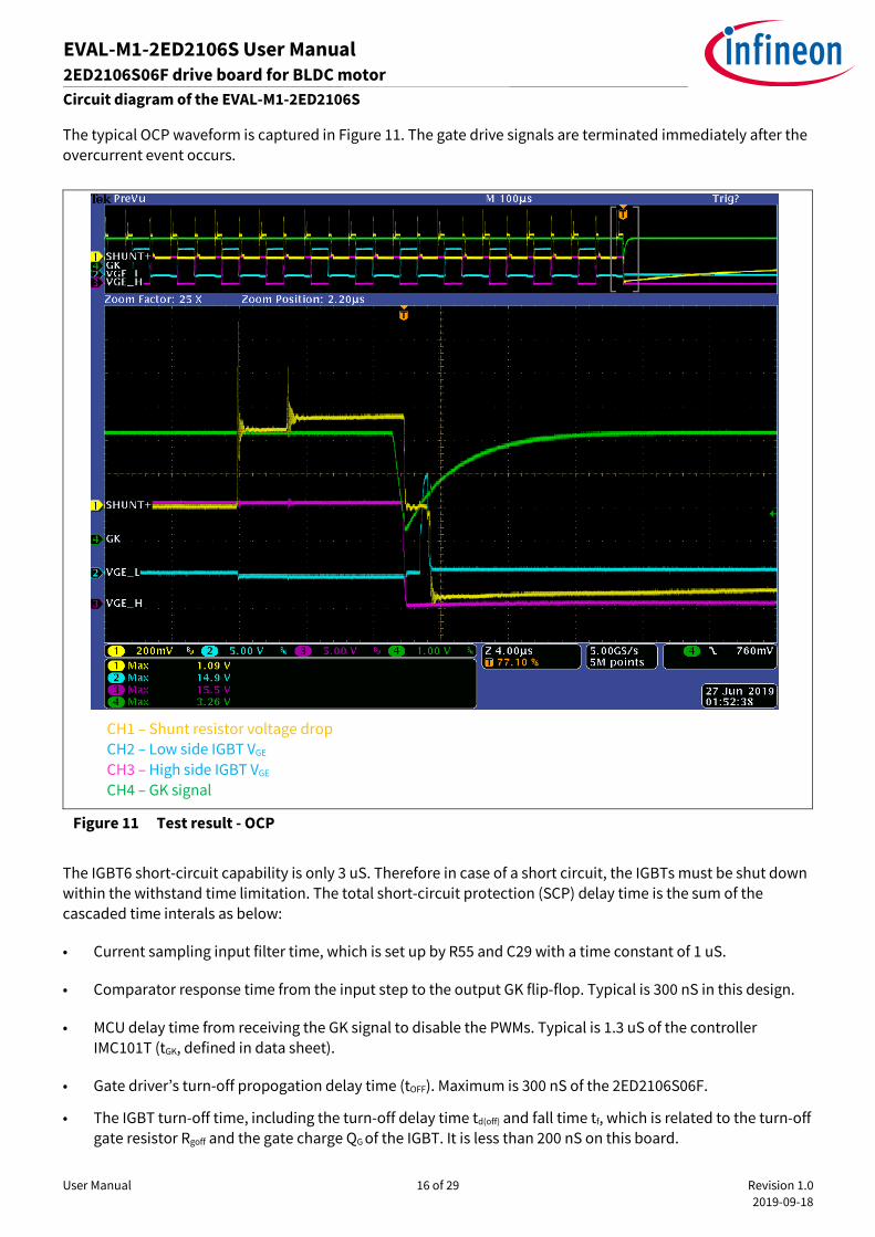
The typical OCP waveform is captured in Figure 11. The gate drive signals are terminated immediately after the
overcurrent event occurs.
Figure 11 Test result - OCP
The IGBT6 short-circuit capability is only 3 uS. Therefore in case of a short circuit, the IGBTs must be shut down
within the withstand time limitation. The total short-circuit protection (SCP) delay time is the sum of the
cascaded time interals as below:
• Current sampling input filter time, which is set up by R55 and C29 with a time constant of 1 uS.
• Comparator response time from the input step to the output GK flip-flop. Typical is 300 nS in this design.
• MCU delay time from receiving the GK signal to disable the PWMs. Typical is 1.3 uS of the controller
IMC101T (tGK, defined in data sheet).
• Gate driver’s turn-off propogation delay time (tOFF). Maximum is 300 nS of the 2ED2106S06F.
• The IGBT turn-off time, including the turn-off delay time td(off) and fall time tf, which is related to the turn-off
gate resistor Rgoff and the gate charge QG of the IGBT. It is less than 200 nS on this board.
CH1 – Shunt resistor voltage drop
CH2 – Low side IGBT VGE
CH3 – High side IGBT VGE
CH4 – GK signal

User Manual 17 of 29 Revision 1.0
2019-09-18
EVAL-M1-2ED2106S User Manual 2ED2106S06F drive board for BLDC motor
Circuit diagram of the EVAL-M1-2ED2106S
The worst-case test of the short circuit was done by linking the high-side IGBT collector and emitter in advance
of the system run. The short circuit would be triggered once the low-side IGBT turns on. In the bench test, the
total SCP delay time of the board was around 2.5 uS (see Figure 12), which meets the IGBT short-circuit
capability.
Figure 12 Test result - SCP
CH1 – Shunt resistor voltage drop
CH2 – Low side IGBT VGE
CH3 – High side IGBT VGE
CH4 – GK signal
User Manual 18 of 29 Revision 1.0
2019-09-18
EVAL-M1-2ED2106S User Manual 2ED2106S06F drive board for BLDC motor
Circuit diagram of the EVAL-M1-2ED2106S
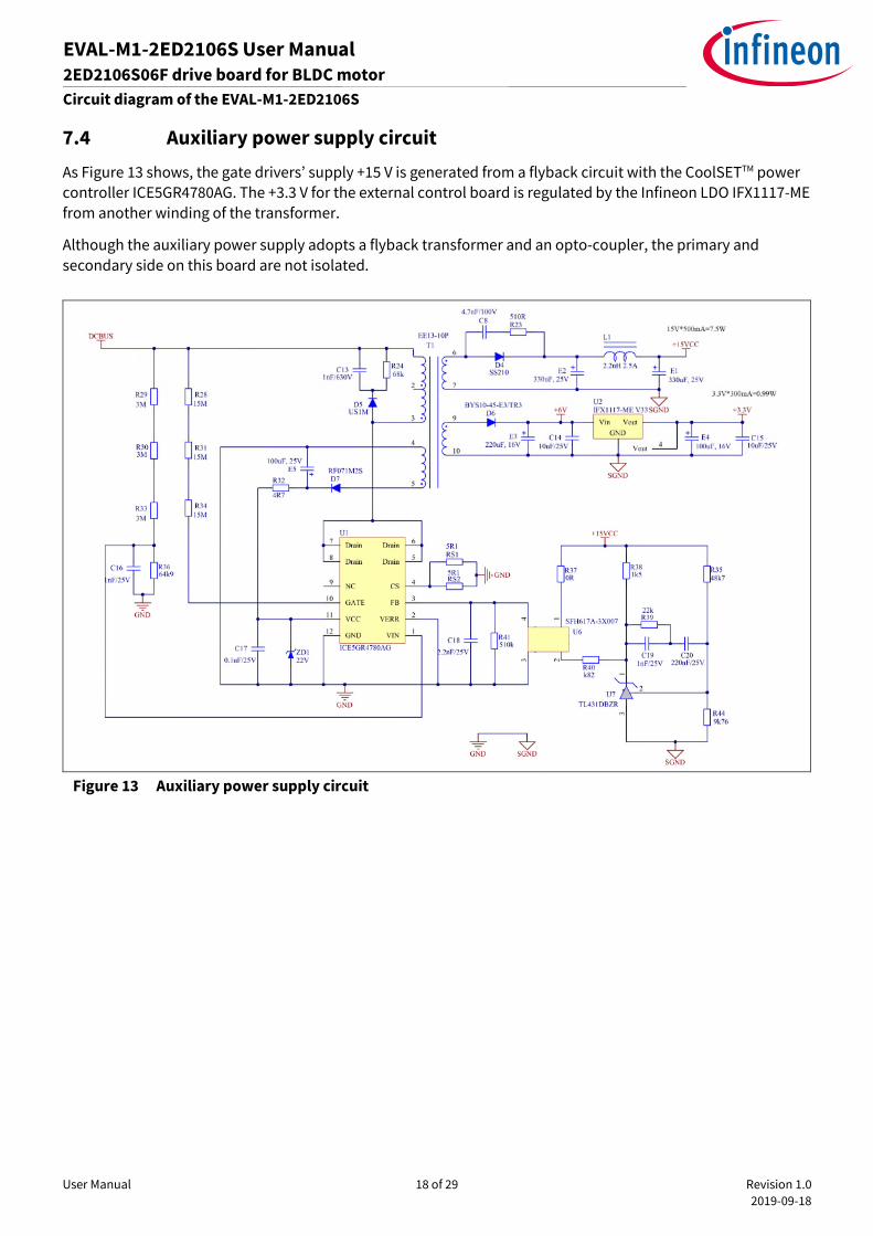
7.4 Auxiliary power supply circuit
As Figure 13 shows, the gate drivers’ supply +15 V is generated from a flyback circuit with the CoolSETTM power
controller ICE5GR4780AG. The +3.3 V for the external control board is regulated by the Infineon LDO IFX1117-ME
from another winding of the transformer.
Although the auxiliary power supply adopts a flyback transformer and an opto-coupler, the primary and
secondary side on this board are not isolated.
Figure 13 Auxiliary power supply circuit

User Manual 19 of 29 Revision 1.0
2019-09-18
EVAL-M1-2ED2106S User Manual 2ED2106S06F drive board for BLDC motor
PCB layout of the EVAL-M1-2ED2106S
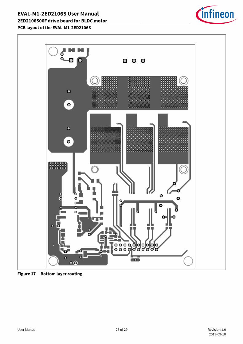
8 PCB layout of the EVAL-M1-2ED2106S
The layout details of the EVAL-M1-2ED2106S can be seen in Figure 14, Figure 15, Figure 16 and Figure 17,
respectively.
Some layout tips are indicated on this board:
• The power conductor paths such as DC+, GND, phase-out, etc. should be as thick as possible for a lower
temperature rise and lower parasitic inductances.
• The shunt resistor is SMD-preferred with the lowest parasitic inductance for a smaller negative VS during
switching.
• The shunt resistor should be located where the LO-COM drive loop is as small as possible.
• The link conductor path of the high-side IGBT-E and low-side IGBT-C should be as thick and short as
possible for a smaller parasitic inductance.
• The power ground and controller ground should be individually copper-filled (in the production process)
and then shorted at the return of the shunt resistor. In this way the LO-COM drive loop parasitic inductance
and the HIN/LIN-COM input signal loop parasitic inductance are both as small as possible (see Figure 15
and Figure 17).
• The VCC and VBS bypass capacitors should be close to the IC.
• Current sensing should be connected directly at the shunt-resistor terminals and sent to the controller
interface as a differential pair.

User Manual 20 of 29 Revision 1.0
2019-09-18
EVAL-M1-2ED2106S User Manual 2ED2106S06F drive board for BLDC motor
PCB layout of the EVAL-M1-2ED2106S
Figure 14 Top assembly drawing

User Manual 21 of 29 Revision 1.0
2019-09-18
EVAL-M1-2ED2106S User Manual 2ED2106S06F drive board for BLDC motor
PCB layout of the EVAL-M1-2ED2106S
Figure 15 Top layer routing

User Manual 22 of 29 Revision 1.0
2019-09-18
EVAL-M1-2ED2106S User Manual 2ED2106S06F drive board for BLDC motor
PCB layout of the EVAL-M1-2ED2106S
Figure 16 Bottom assembly drawing
User Manual 23 of 29 Revision 1.0
2019-09-18
EVAL-M1-2ED2106S User Manual 2ED2106S06F drive board for BLDC motor
PCB layout of the EVAL-M1-2ED2106S
Figure 17 Bottom layer routing

User Manual 24 of 29 Revision 1.0
2019-09-18
EVAL-M1-2ED2106S User Manual 2ED2106S06F drive board for BLDC motor
Bill of material
9 Bill of material
All the components of the EVAL-M1-2ED2106S board are listed in Table 7.
Table 7 Bill of material
Designator Description Footprint Vendor Part number Quantity
BUS OK,
VCC OK
LED RED CLEAR ROUND T/H
Diameter 3 mm P=2.54 mm
Wurth
Electronics
151034RS03000 2
C3, C4, C5 MLCC 2.2 uF 25 V X7R M 1206 Wurth
Electronics
885012208066 3
C8 MLCC 4.7 nF 100 V X7R M 1206 Wurth
Electronics
885012208110 1
C13 MLCC 1 nF 630 V X5R M 1206 Wurth
Electronics
885342208011 1
C14, C15,
C27 MLCC 10 uF 16 V X5R M
0805 Wurth
Electronics
885012107014 3
C16, C19,
C29 MLCC 1 nF 25 V X7R M
0805 Wurth
Electronics
885012207060 3
C17, C21,
C22, C23,
C24, C34
MLCC 0.1 uF 25 V X7R M
0805 Wurth
Electronics
885012207072
6
C18 MLCC 2.2 nF 25 V X7R M 0805 Wurth
Electronics
885012207062 1
C20 MLCC 220 nF 25 V X7R M 0805 Wurth
Electronics
885012207074 1
C26 DNI 0805 1
C28 MLCC 4.7 nF 25 V X5R M 0805 Wurth
Electronics
885012207064 1
C30, C31,
C32, C33 MLCC 10 uF 25 V X5R M
1206 Wurth
Electronics
885012208069 4
COM, HIN,
HO, LIN, LO,
VB, VCC, VS
Test Point – Miniature
White Diameter 2.54 mm
Keystone
Electronics
5002
8
D1, D2, D3,
D8, D9, D10
Small Signal Fast Switching
Diode 150 mA 75 V
SOD-123 Vishay 1N4148W-G 6
D4 Schottky Diode 1.5 A 100 V SMB Vishay SS210 1
D5 Ultra Fast Diode 1 A 1000 V SMA Vishay US1M 1
D6 Schottky Diode 1.5 A 45 V SMA Vishay BYS10-45 1
D7 Super Fast Diode 700 mA
200 V 25 nS
SOD-123 ROHM RF071MM2S 1
E1, E2 ECAP AL LD 330 uF 25 V M 8*11.5 mm
P3.5 mm
Wurth
Electronics
860020474013 2
E3 ECAP AL LD 220 uF 16 V M 8*11.5 mm
P3.5 mm
Wurth
Electronics
860010374011 1

User Manual 25 of 29 Revision 1.0
2019-09-18
EVAL-M1-2ED2106S User Manual 2ED2106S06F drive board for BLDC motor
Bill of material
Designator Description Footprint Vendor Part number Quantity
E4 ECAP AL LD 100 uF 16 V M 8*11.5 mm
P3.5 mm
Wurth
Electronics
860240374004 1
E5, E8 ECAP AL 100 uF 25 V M 6.3*11 mm
P2.5 mm
Wurth
Electronics
860020473008 2
E6, E7 ECAP AL 47 uF 400 V M 18*21 mm
P7.5 mm
Wurth
Electronics
860241381005 2
HTSK Heatsink 55x55 mm 1
J2 Horizontal Cable Entry with
Rising Cage Clamp
3-way 5.08
mm
Wurth
Electronics
691216510003S 1
J3 Horizontal Cable Entry with
Rising Cage Clamp
2-way 5.08
mm
Wurth
Electronics
691216510002S 1
J5 Angled Dual Socket
Header
20-pin 2.54
mm
Wurth
Electronics
613020243121 1
L1 SMD Power Inductor 2.2 uH
+/-20% 2.5 A
SMD Wurth
Electronics
744773022 1
Q1, Q2, Q3,
Q4, Q5, Q6 10 A 650 V IGBT6
D2PAK Infineon IKB10N65ET6 6
R1, R2, R3,
R4, R5, R6, RES SMD 100Ω 5%
0805 Yageo RC0805JR-07100RL6
R10, R11,
R12, R13,
R14, R15
RES SMD 150 Ω 5%
0805 Yageo RC0805JR-07150RL
6
R7, R8, R9,
R54, R56,
R57
RES SMD 47 Ω 5%
0805 Yageo RC0805JR-0747RL
6
R16 RES SMD 100 mΩ 3 W 1% 1225 Viking CS25FTER100 1
R17, R18,
R19, R20,
R21, R22
RES SMD 10 kΩ 5%
0805 Yageo RC0805JR-0710KL
6
R23 RES SMD 510 Ω 5% 1206 Yageo RC1206JR-07510RL 1
R24 RES SMD 68 kΩ 5% 1206 Yageo RC1206JR-0768KL 1
R25, R26,
R27, R47 RES SMD 499 kΩ 1%
0805 Yageo RC0805FR-07499KL4
R28, R31,
R34 RES SMD 15 MΩ 5%
1206 Yageo RC1206JR-0715ML3
R29, R30,
R33 RES SMD 3 MΩ 5%
1206 Yageo RC1206JR-073ML3
R32 RES SMD 4.7 Ω 5% 1206 Yageo RC1206JR-074R7L 1
R35 RES SMD 48.7 kΩ 1% 0805 Yageo RC0805FR-0748K7L 1
R36 RES SMD 64.9 kΩ 1% 0805 Yageo RC0805FR-0764K9L 1
R37, R42,
R43, R45 RES SMD 0 Ω 5%
0805 Yageo RC0805JR-070RL4
R38 RES SMD 1.5 kΩ 1% 0805 Yageo RC0805FR-071K5L 1

User Manual 26 of 29 Revision 1.0
2019-09-18
EVAL-M1-2ED2106S User Manual 2ED2106S06F drive board for BLDC motor
Bill of material
Designator Description Footprint Vendor Part number Quantity
R39 RES SMD 22 kΩ 1% 0805 Yageo RC0805FR-0722KL 1
R40 RES SMD 820 Ω 1% 0805 Yageo RC0805FR-07820RL 1
R41 RES SMD 510 kΩ 5% 0805 Yageo RC0805JR-07510KL 1
R44 RES SMD 9.76 kΩ 1% 0805 Yageo RC0805FR-079K76L 1
R46, R52 RES SMD 5.1 kΩ 1% 0805 Yageo RC0805FR-075K1L 2
R48 DNI 1
R49, R50,
R58 RES SMD 390 kΩ 5%
1206 Yageo RC1206JR-07390KL3
R51, R55 RES SMD 1 kΩ 5% 0805 Yageo RC0805JR-071KL 2
R53 RES SMD 1.02 kΩ 1% 0805 Yageo RC0805FR-071K02L 1
RS1, RS2 RES SMD 5.1 Ω 1% 1206 Yageo RC1206FR-075R1L 2
T1 Flyback Transformer EE13
3.5 mH
EE13-10P Wurth
Electronics
-- 1
U1 CoolSETTM power controller DSO-12 Infineon
Technologies
ICE5GR4780AG 1
U2 LDO output 3.3 V SOT-223-4 Infineon
Technologies
IFX1117ME
V33HTMA1 1
U3, U4, U5 650 V SOI high side and low
side gate driver
DSO-8 Infineon
Technologies
2ED2106S06F 3
U6 OptoCoupler 60 mA 70 V
CTR 100%-200%
SMD-4,
option 7
Vishay SFH617A-3X007 1
U7 Precision Programmable
Reference
SOT-23 Texas
Instruments
TL431DBZR 1
U8 Dual Differential
Comparator
SO-8 Texas
Instruments
LM393ADR 1
ZD1 Zener Diode 22 V 500 mW SOD-123 Vishay MMSZ5251B 1
ZD2 Zener Diode 10 V 500 mW SOD-123 Vishay MMSZ5240B 1
Sil-pad 60*60 mm, thickness
0.23mm
SP900S 1

User Manual 27 of 29 Revision 1.0
2019-09-18
EVAL-M1-2ED2106S User Manual 2ED2106S06F drive board for BLDC motor
Reference
10 Reference
[1] Data sheet of Infineon Technologies 2ED2106S06F
[2] Data sheet of Infineon Technologies IR2106S
[3] Data sheet of Infineon Technologies IRS2106S
[4] Data sheet of Infineon Technologies IMC101T
[5] Data sheet of Texas Instruments LM393A
[6] Application Note AN2018-01 EVAL-M1-101T User’s Manual
Note: All listed data sheets and application notes of Infineon parts are available for downloading from
Infineon’s website www.infineon.com/.

User Manual 28 of 29 Revision 1.0
2019-09-18
EVAL-M1-2ED2106S Application Note 2ED2106S06F Drive Board for BLDC motor
Revision history
Revision history
Document
version
Date of release Description of changes
1.0 2019-09-18 First release

Trademarks All referenced product or service names and trademarks are the property of their respective owners.
Edition 2019-09-18
AN2019-19
Published by
Infineon Technologies AG
81726 Munich, Germany
© 2019 Infineon Technologies AG.
All Rights Reserved.
Do you have a question about this
document?
Email: [email protected]
Document reference
IMPORTANT NOTICE The information contained in this application note is given as a hint for the implementation of the product only and shall in no event be regarded as a description or warranty of a certain functionality, condition or quality of the product. Before implementation of the product, the recipient of this application note must verify any function and other technical information given herein in the real application. Infineon Technologies hereby disclaims any and all warranties and liabilities of any kind (including without limitation warranties of non-infringement of intellectual property rights of any third party) with respect to any and all information given in this application note.
The data contained in this document is exclusively intended for technically trained staff. It is the responsibility of customer’s technical departments to evaluate the suitability of the product for the intended application and the completeness of the product information given in this document with respect to such application.
For further information on the product, technology, delivery terms and conditions and prices please contact your nearest Infineon Technologies office (www.infineon.com).
WARNINGS Due to technical requirements products may contain dangerous substances. For information on the types in question please contact your nearest Infineon Technologies office.
Except as otherwise explicitly approved by Infineon Technologies in a written document signed by authorized representatives of Infineon Technologies, Infineon Technologies’ products may not be used in any applications where a failure of the product or any consequences of the use thereof can reasonably be expected to result in personal injury.