EUV Lithography –Status and Key Challenges for HVM ...
38
EUV Lithography – Status and Key Challenges for HVM Implementation Sam Sivakumar Intel Corporation
Transcript of EUV Lithography –Status and Key Challenges for HVM ...
EUV Lithography – Status and Key Challenges for HVM Implementation
Sam Sivakumar
Intel Corporation
2
Sivakumar2009 International Symposium on EUV Lithography
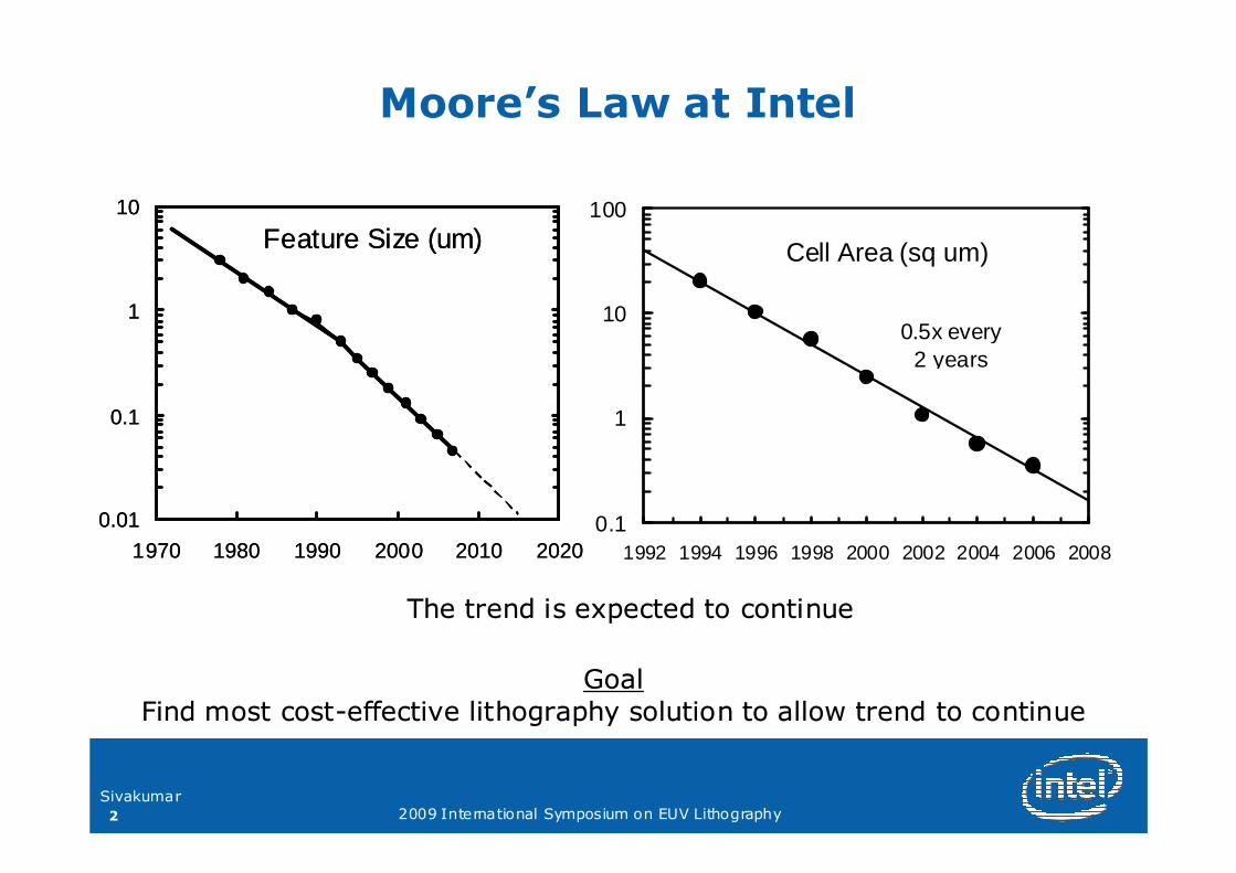
Moore’s Law at Intel
Feature Size (um)
0.01
0.1
1
10
1970 1980 1990 2000 2010 2020
Feature Size (um)
0.01
0.1
1
10
1970 1980 1990 2000 2010 2020
The trend is expected to continueThe trend is expected to continue
Cell Area (sq um)
0.1
1
10
100
1992 1994 1996 1998 2000 2002 2004 2006 2008
0.5x every 2 years
GoalGoal
Find most costFind most cost--effective lithography solution to allow trend to continueeffective lithography solution to allow trend to continue

3
Sivakumar2009 International Symposium on EUV Lithography
Choosing between Lithography Options
� If current lithography is capable of delivering a manufacturable process, use it
� If not:
–If new lithography technology is ready, manufacturable and cost-effective, use it (increase NA, reduce λ)
–If not:
– need to make alternative decisions to enable scaling without litho improvements (operate more effectively at lower k1)
Managing litho transitions is key! Requires significant planninManaging litho transitions is key! Requires significant planningg
4
Sivakumar2009 International Symposium on EUV Lithography
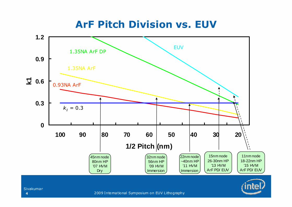
0
0.3
0.6
0.9
1.2
100 90 80 70 60 50 40 30 20
1/2 Pitch (nm)
k1
EUVEUV1.35NA 1.35NA ArFArF DPDP
1.35NA 1.35NA ArFArF
0.93NA 0.93NA ArFArF
kk11 = 0.3= 0.3
ArF Pitch Division vs. EUV
45nm node80nm HP’07 HVM
Dry
32nm node56nm HP’09 HVM
Immersion
22nm node~40nm HP’11 HVM
Immersion
15nm node26-30nm HP
’13 HVMArF PD/ EUV
11nm node18-22nm HP
’15 HVMArF PD/ EUV
5
Sivakumar2009 International Symposium on EUV Lithography
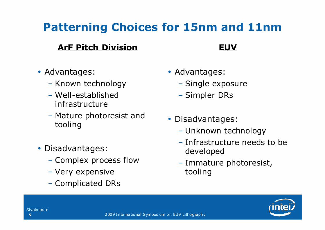
Patterning Choices for 15nm and 11nm
ArF Pitch Division
� Advantages:
– Known technology
– Well-established infrastructure
– Mature photoresist and tooling
� Disadvantages:
– Complex process flow
– Very expensive
– Complicated DRs
EUV
� Advantages:
– Single exposure
– Simpler DRs
� Disadvantages:
– Unknown technology
– Infrastructure needs to be developed
– Immature photoresist, tooling
6
Sivakumar2009 International Symposium on EUV Lithography
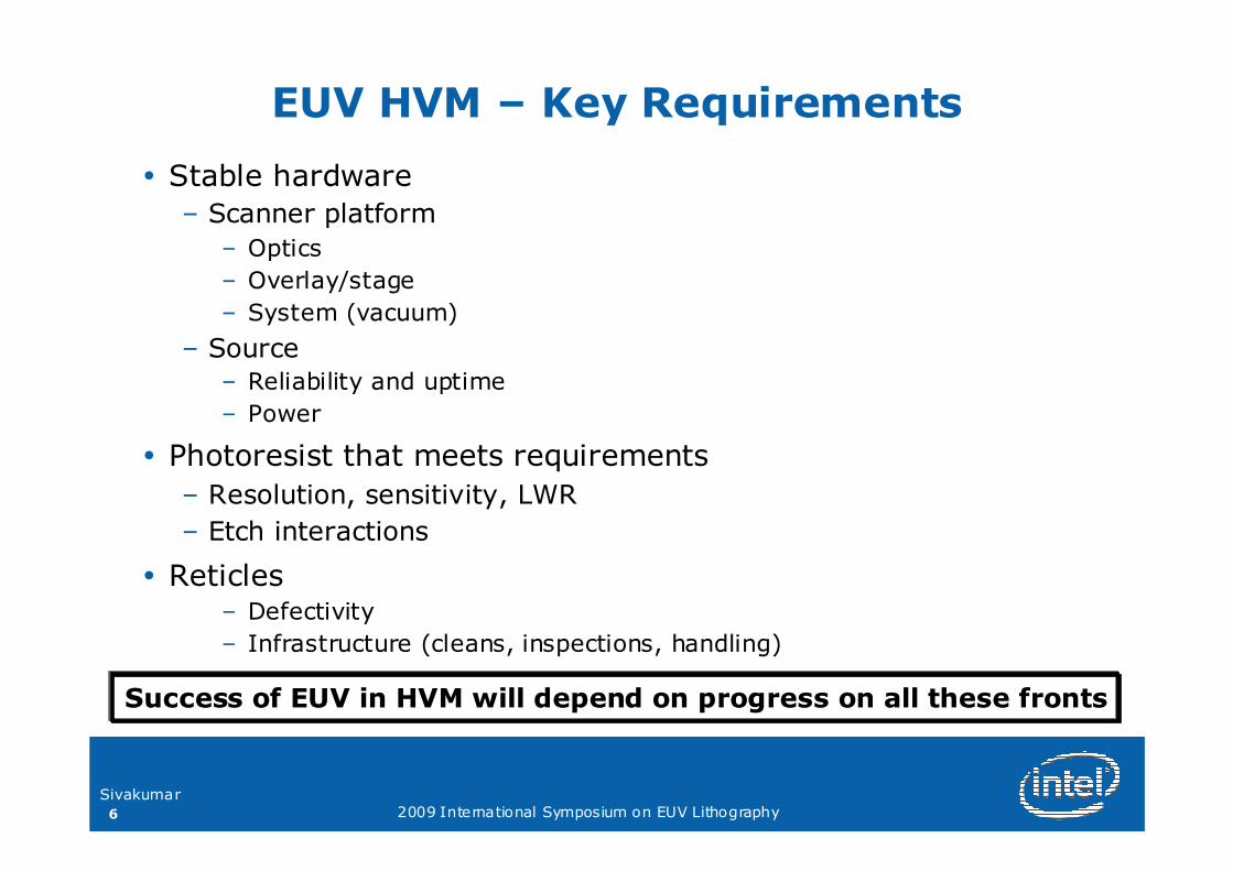
EUV HVM – Key Requirements
� Stable hardware
– Scanner platform
– Optics
– Overlay/stage
– System (vacuum)
– Source
– Reliability and uptime
– Power
� Photoresist that meets requirements
– Resolution, sensitivity, LWR
– Etch interactions
� Reticles– Defectivity
– Infrastructure (cleans, inspections, handling)
Success of EUV in HVM will depend on progress on all these frontSuccess of EUV in HVM will depend on progress on all these frontss

7
Sivakumar2009 International Symposium on EUV Lithography
Exposure Tooling
8
Sivakumar2009 International Symposium on EUV Lithography
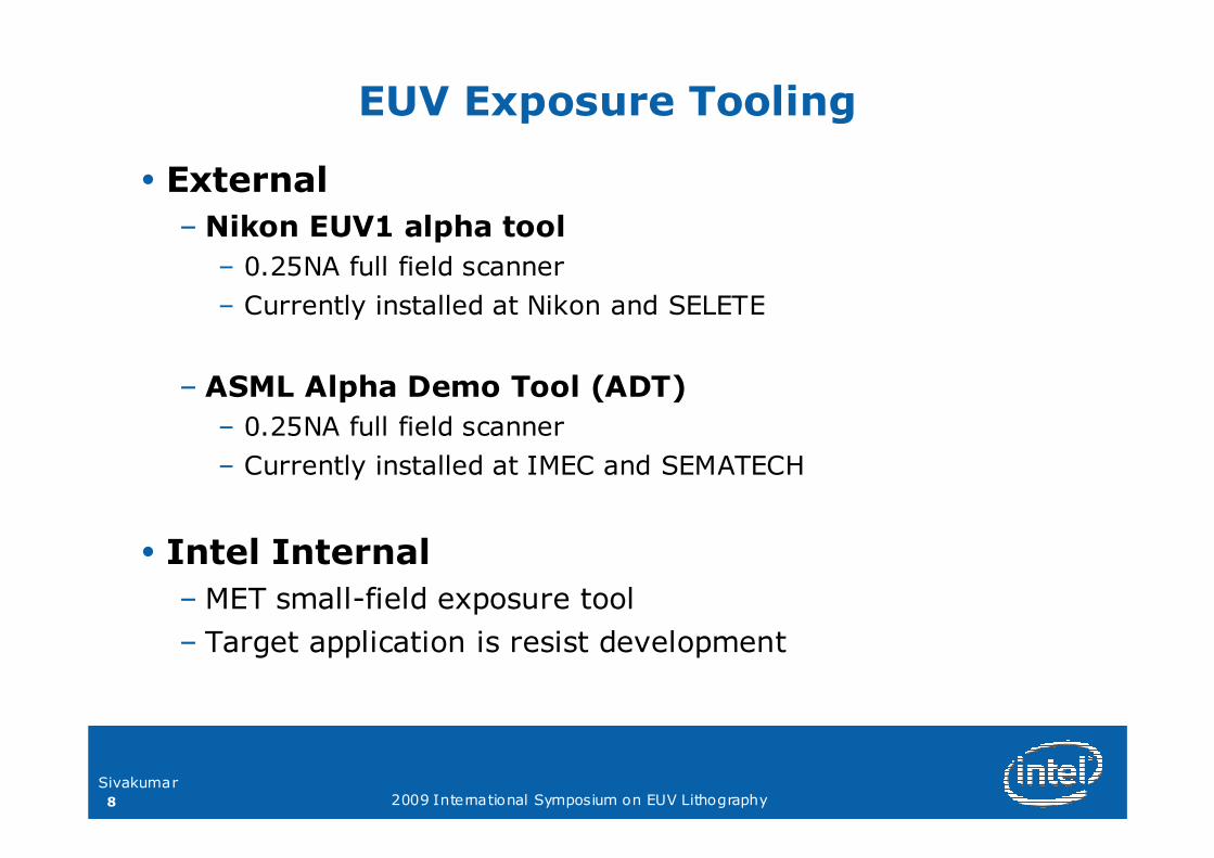
EUV Exposure Tooling
� External
– Nikon EUV1 alpha tool
– 0.25NA full field scanner
– Currently installed at Nikon and SELETE
– ASML Alpha Demo Tool (ADT)
– 0.25NA full field scanner
– Currently installed at IMEC and SEMATECH
� Intel Internal
– MET small-field exposure tool
– Target application is resist development
9
Sivakumar2009 International Symposium on EUV Lithography
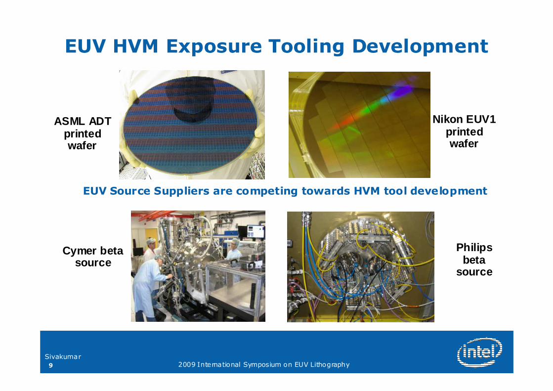
EUV HVM Exposure Tooling Development
EUV Source Suppliers are competing towards HVM tool development
Nikon EUV1 printed wafer
Philips beta
source
ASML ADT printed wafer
Cymer beta source
10
Sivakumar2009 International Symposium on EUV Lithography
Photoresists

11
Sivakumar2009 International Symposium on EUV Lithography
Source: (XTREME DPF Source)
0.5mm x 2mm (FWHM)
35W EUV in 2ππππ
Intel MET •• 0.3NA capability0.3NA capability
•• 600 x 600 600 x 600 µµm fieldm field
•• Low flare (3 Low flare (3 --6%)6%)
• New EUV collector installed
• New outer shell extended σouter from 0.55 to 0.65, 22nm HP resolution with quadrupole illumination
• First step in preparation for 0.5 NA MET projection optics (2010) that will enable ~10nm HP resolution

12
Sivakumar2009 International Symposium on EUV Lithography
Intel MET Status
� Uptime average: 67% in ‘07, 85% in ‘08, 65% through WW38 in ‘09
� Continuous improvement in output efficiency –14J/cm2/day currently
� On track to deliver more dose in 2009 than in 2008
� Improved resolution and expanded process window
� Long term upgrade path defined down to ~10nm HP
> 250 Resists Screened in > 250 Resists Screened in ’’08. Goal 08. Goal >> 500 in 500 in ’’0909
MET Cumulative Dose (J/cm2)
0
1000
2000
3000
4000
5000
6000
70000
200
400
600
800
1000
1200
1400
1600
1800
Day
J/cm
2
2H '04 (Install/Qual)20052006200720082009 (through WW37)
3.8 J/cm2 per day
7.1 J/cm2 per day
1 J/cm2 per day
14 J/cm2 per day
13
Sivakumar2009 International Symposium on EUV Lithography
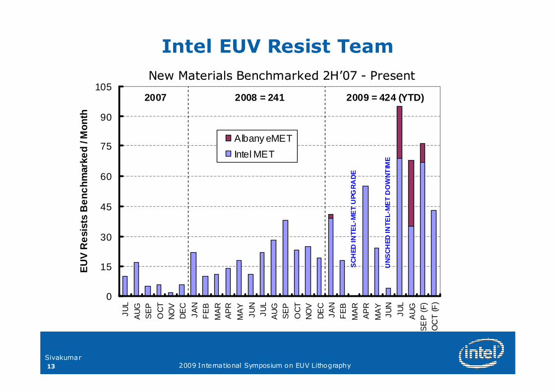
Intel EUV Resist Team
0
15
30
45
60
75
90
105
JUL
AU
GS
EP
OC
TN
OV
DE
C
JAN
FE
B
MA
RA
PR
MA
Y
JUN
JUL
AU
GS
EP
OC
TN
OV
DE
CJA
NF
EB
MA
RA
PR
MA
YJU
N
JUL
AU
GS
EP
(F)
OC
T (F
)
EU
V R
esi
sts
Be
nc
hm
arke
d /
Mo
nth
Albany eMET
Intel MET
2007 2008 = 241 2009 = 424 (YTD)
SC
HED
INTE
L-M
ET
UPG
RA
DE
UN
SC
HED
INTE
L-M
ET
DO
WN
TIM
E
New Materials Benchmarked 2HNew Materials Benchmarked 2H’’07 07 -- PresentPresent
14
Sivakumar2009 International Symposium on EUV Lithography
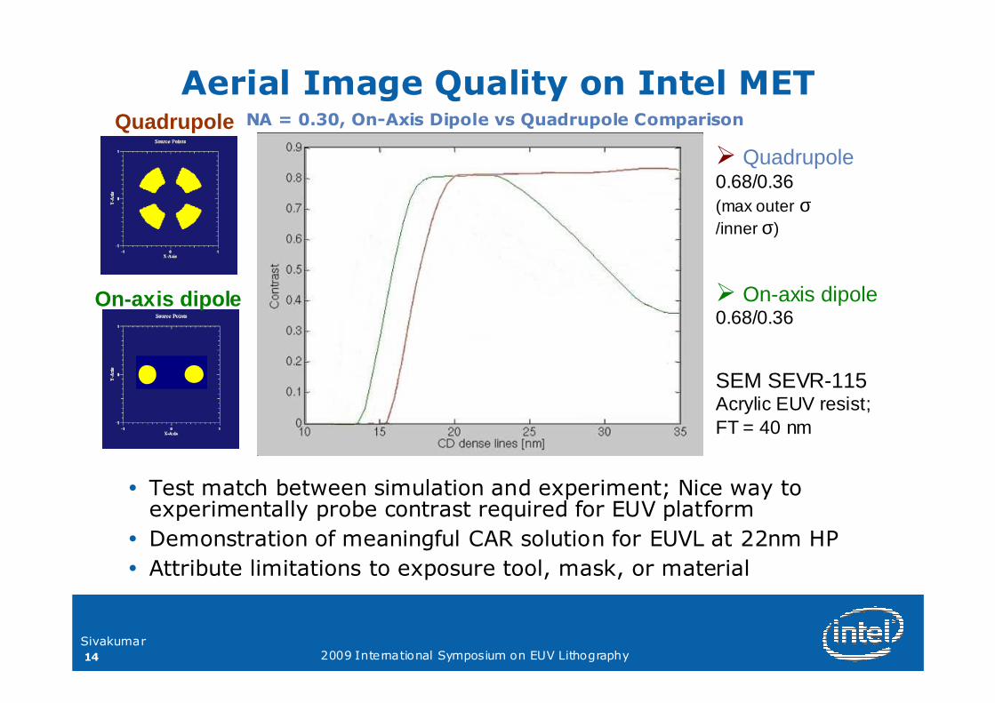
Aerial Image Quality on Intel MET
� Test match between simulation and experiment; Nice way to experimentally probe contrast required for EUV platform
� Demonstration of meaningful CAR solution for EUVL at 22nm HP
� Attribute limitations to exposure tool, mask, or material
On-axis dipole
Quadrupole
� Quadrupole0.68/0.36(max outer σ/inner σ)
� On-axis dipole0.68/0.36
SEM SEVR-115Acrylic EUV resist; FT = 40 nm
NA = 0.30, On-Axis Dipole vs Quadrupole Comparison
15
Sivakumar2009 International Symposium on EUV Lithography
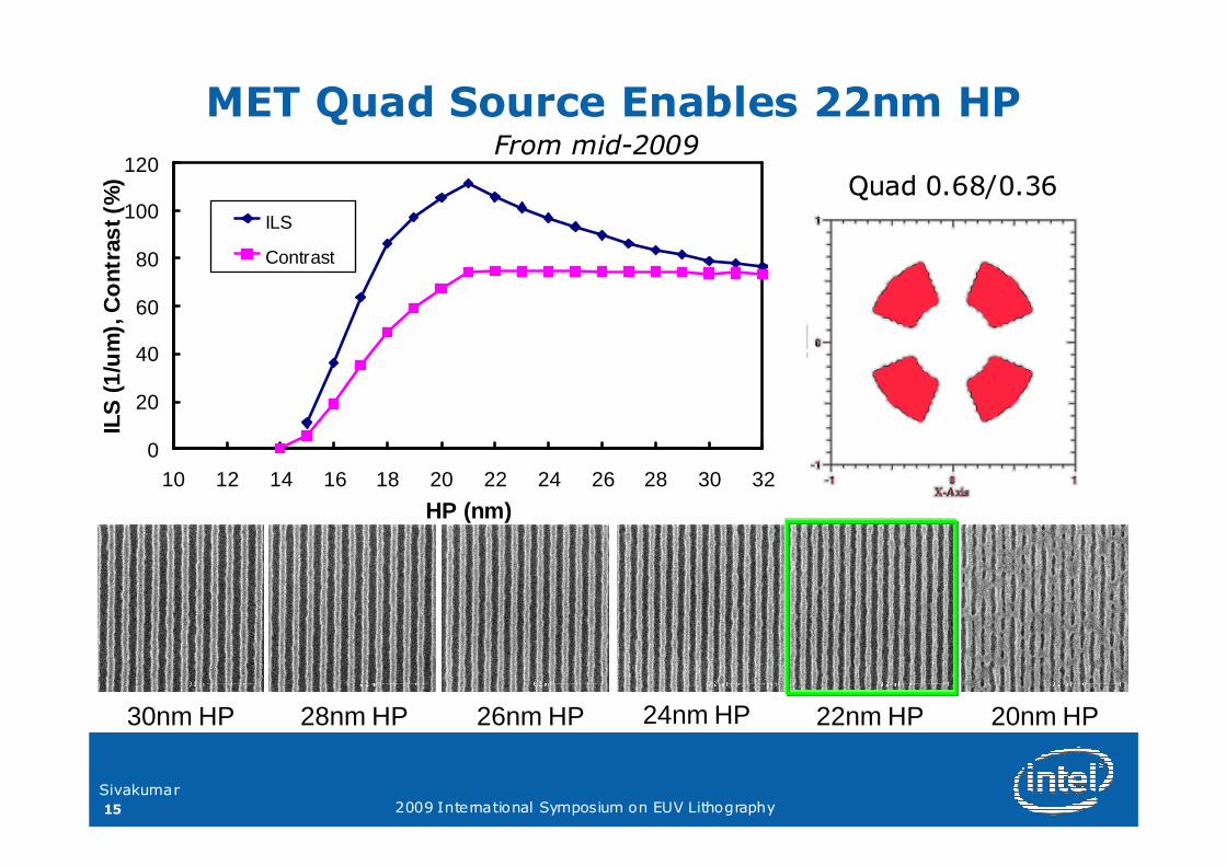
MET Quad Source Enables 22nm HP
0
20
40
60
80
100
120
10 12 14 16 18 20 22 24 26 28 30 32
HP (nm)
ILS
(1/u
m),
Co
ntra
st (
%)
ILS
Contrast
30nm HP 28nm HP 26nm HP 24nm HP 22nm HP 20nm HP
Quad 0.68/0.36Quad 0.68/0.36
From midFrom mid--20092009
16
Sivakumar2009 International Symposium on EUV Lithography
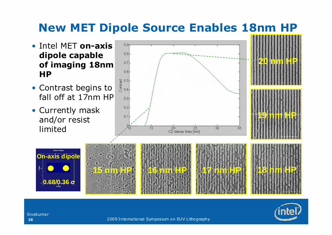
New MET Dipole Source Enables 18nm HP
20 nm HP
19 nm HP
18 nm HP17 nm HP16 nm HP15 nm HP
• Intel MET on-axis dipole capable of imaging 18nm HP
• Contrast begins to fall off at 17nm HP
• Currently mask and/or resist limited
On-axis dipole
0.68/0.36 σ
17
Sivakumar2009 International Symposium on EUV Lithography
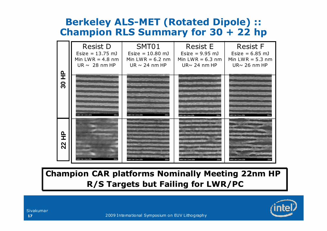
Berkeley ALS-MET (Rotated Dipole) :: Champion RLS Summary for 30 + 22 hp
SMT01Esize = 10.80 mJ
Min LWR = 6.2 nm
UR ~ 24 nm HP
Resist DEsize = 13.75 mJ
Min LWR = 4.8 nm
UR ~ 28 nm HP
Resist FEsize = 6.85 mJ
Min LWR = 5.3 nm
UR~ 26 nm HP
Resist EEsize = 9.95 mJ
Min LWR = 6.3 nm
UR~ 24 nm HP 22
HP
30 H
P
Champion CAR platforms Nominally Meeting 22nm HP Champion CAR platforms Nominally Meeting 22nm HP
R/S Targets but Failing for LWR/PCR/S Targets but Failing for LWR/PC

18
Sivakumar2009 International Symposium on EUV Lithography
Pattern Collapse Margin Improvement
Multiple approaches may be needed to address problem
– Modify Aspect Ratio
– Surface (Energy) Optimization: Hydrophobicity, Multilayer stacks
– Increased resist modulus, Negative Tone & Semi-organic Resists
– Decreased Surface Tension: Rinse agents, Organic Developers, Develop/Rinse/Spin Dry Process Optimization
Pattern Collapse Mitigation is a key area of focusPattern Collapse Mitigation is a key area of focus
19
Sivakumar2009 International Symposium on EUV Lithography
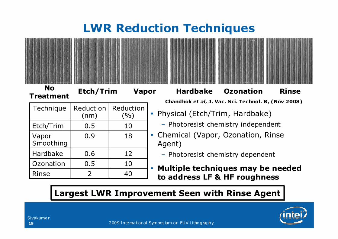
LWR Reduction Techniques
� Physical (Etch/Trim, Hardbake)
– Photoresist chemistry independent
� Chemical (Vapor, Ozonation, Rinse
Agent)
– Photoresist chemistry dependent
� Multiple techniques may be needed
to address LF & HF roughness
No Treatment
Etch/Trim OzonationHardbakeVapor Rinse
Chandhok et al, J. Vac. Sci. Technol. B, (Nov 2008)
402Rinse
100.5Ozonation
120.6Hardbake
180.9Vapor Smoothing
100.5Etch/Trim
Reduction (%)
Reduction (nm)
Technique
Largest LWR Improvement Seen with Rinse AgentLargest LWR Improvement Seen with Rinse Agent

20
Sivakumar2009 International Symposium on EUV Lithography
Resist and Tooling Gaps
2X/5XNone/2XImprovement Required
1.9/1.2810Target
3.8/6.410/20Current
3σ LWR (nm)Photospeed (mJ/cm2)
PhotoresistsPhotoresists (32/22nm HP)(32/22nm HP)
10XImprovement Required
200Target
~20Current
Power (W)
Source PowerSource Power
20XImprovement Required
100Target
5Current
Runrate (wph)
Scanner Scanner RunrateRunrate
Summary:Summary:
Good progress made to dateGood progress made to date
Need continued work to bridge (or significantly reduce) gaps forNeed continued work to bridge (or significantly reduce) gaps forboth performance and COOboth performance and COO

21
Sivakumar2009 International Symposium on EUV Lithography
Reticles
22
Sivakumar2009 International Symposium on EUV Lithography
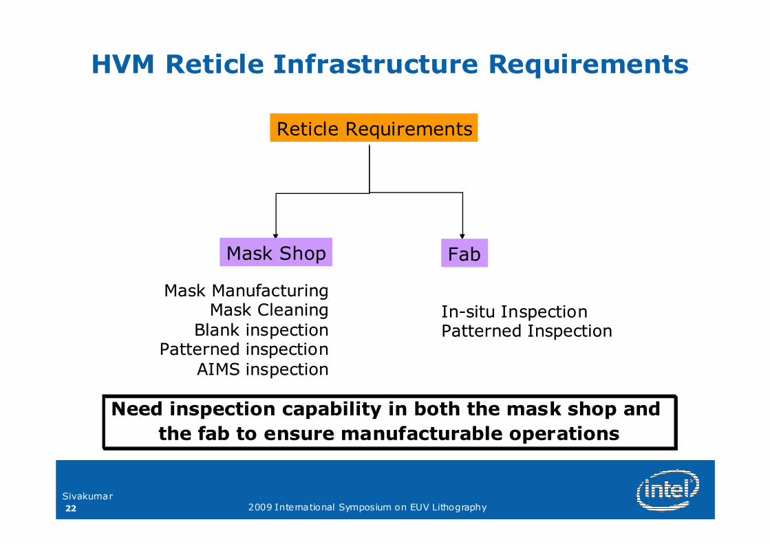
HVM Reticle Infrastructure Requirements
Reticle Requirements
Mask Shop Fab
Mask ManufacturingMask ManufacturingMask CleaningMask Cleaning
Blank inspectionBlank inspectionPatterned inspectionPatterned inspection
AIMS inspectionAIMS inspection
InIn--situ Inspectionsitu InspectionPatterned InspectionPatterned Inspection
Need inspection capability in both the mask shop and Need inspection capability in both the mask shop and
the the fabfab to ensure to ensure manufacturablemanufacturable operationsoperations

23
Sivakumar2009 International Symposium on EUV Lithography
Intel’s Mask Tool Pilot Line
EUV AIMS
1G & 2G Blank Inspection EUV ReflFlatness
Sorter
Film Dep
Mask Clean
3GActinic Blank
Inspection
Patterned mask
inspection
24
Sivakumar2009 International Symposium on EUV Lithography
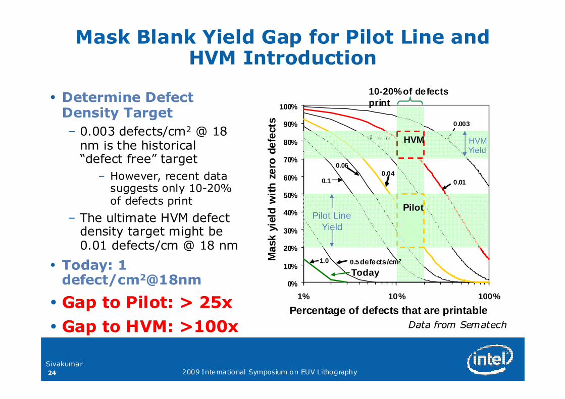
Mask Blank Yield Gap for Pilot Line and HVM Introduction
� Determine Defect Density Target
– 0.003 defects/cm2 @ 18 nm is the historical “defect free” target
– However, recent data suggests only 10-20% of defects print
– The ultimate HVM defect density target might be 0.01 defects/cm @ 18 nm
� Today: 1 defect/cm2@18nm
� Gap to Pilot: > 25x
� Gap to HVM: >100x
0%
10%
20%
30%
40%
50%
60%
70%
80%
90%
100%
1% 10% 100%
1.0 0.5
0.10.04
0.01
0.003
0.06
0.02
Mas
k yi
eld
wit
h z
ero
def
ects
Percentage of defects that are printable
HVM
Pilot
defects/cm2
10-20% of defects print
Pilot Line Yield
HVMYield
Today
Data from Data from SematechSematech
25
Sivakumar2009 International Symposium on EUV Lithography
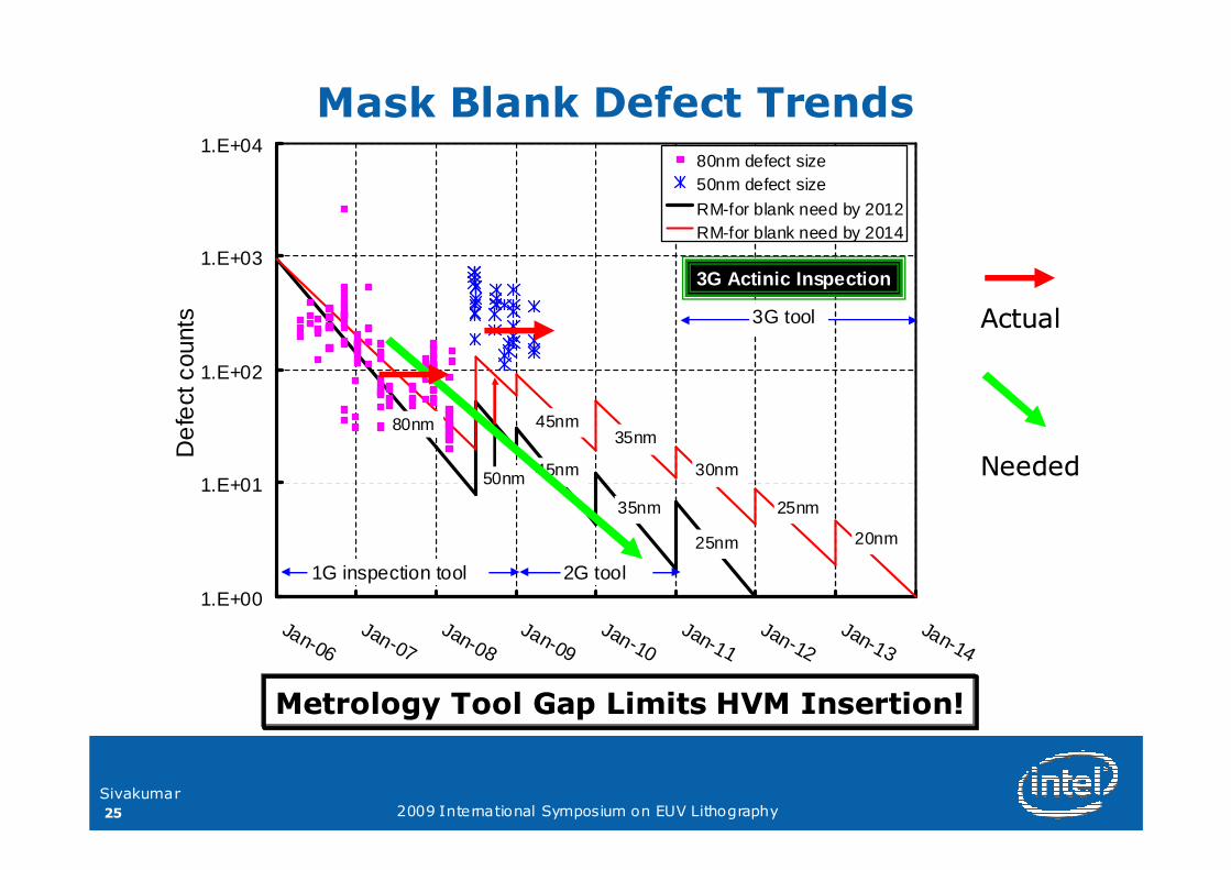
Mask Blank Defect Trends
1.E+00
1.E+01
1.E+02
1.E+03
1.E+04
Jan-06Jan-07
Jan-08Jan-09
Jan-10Jan-11
Jan-12Jan-13
Jan-14
De
fect
cou
nts
80nm defect size50nm defect size
RM-for blank need by 2012RM-for blank need by 2014
80nm
50nm 45nm
35nm
25nm
2G tool1G inspection tool
3G tool
30nm
25nm
20nm
45nm35nm
3G Actinic Inspection
Metrology Tool Gap Limits HVM Insertion!Metrology Tool Gap Limits HVM Insertion!
ActualActual
NeededNeeded
26
Sivakumar2009 International Symposium on EUV Lithography
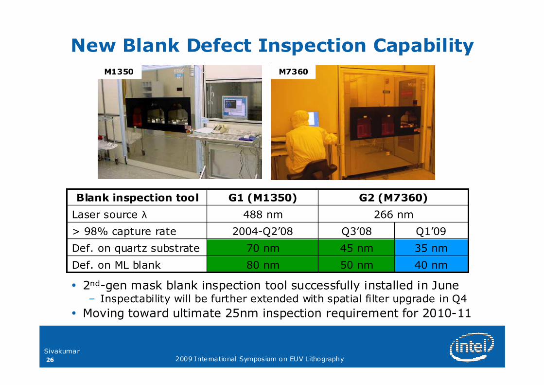
New Blank Defect Inspection Capability
� 2nd-gen mask blank inspection tool successfully installed in June– Inspectability will be further extended with spatial filter upgrade in Q4
� Moving toward ultimate 25nm inspection requirement for 2010-11
M1350 M7360
266 nm488 nmLaser source λ
40 nm50 nm80 nmDef. on ML blank
35 nm45 nm70 nmDef. on quartz substrate
Q1’09Q3’082004-Q2’08> 98% capture rate
G2 (M7360)G1 (M1350)Blank inspection tool
27
Sivakumar2009 International Symposium on EUV Lithography
AIMS and Patterned Defect Inspections
AIMS:
– Industry requirement:
– 22nm hp+ defect repair verification with scanner conditions
– Strategy for 2013 HVM:
– HVM tool requires commercial partner, but market is small
– Consortium model attempts underway – July summit
Patterned:
– Industry Requirement:
– Patterned defect inspection at 22nm HP
– KLA6XX will achieve 32nm and some 22nm HP performance
– Strategy for 2013 HVM:
– Market is sizeable and tool cost significant
– Suppliers unwilling to bear $250M NRE cost alone – July summit
– SEMATECH contribution will be to broker funding model
28
Sivakumar2009 International Symposium on EUV Lithography
July Semicon Meeting on EUV Reticles
� Meeting was held with good participation from suppliers, mask shops, IDM’s, and consortia.
� Technical and business working groups have been busy
– Available data has been shared and leveraged as appropriate
– Some additional data collection underway to validate specs
– Stakeholders should provide clear feedback on funding models
– A benefit for assuming risk is equivalent to a penalty for standing by (e.g. ROFRs, royalties, etc.)
� Letters of Intent will be requested this year, commitments early 2010
� Now is the time to get on board!
29
Sivakumar2009 International Symposium on EUV Lithography
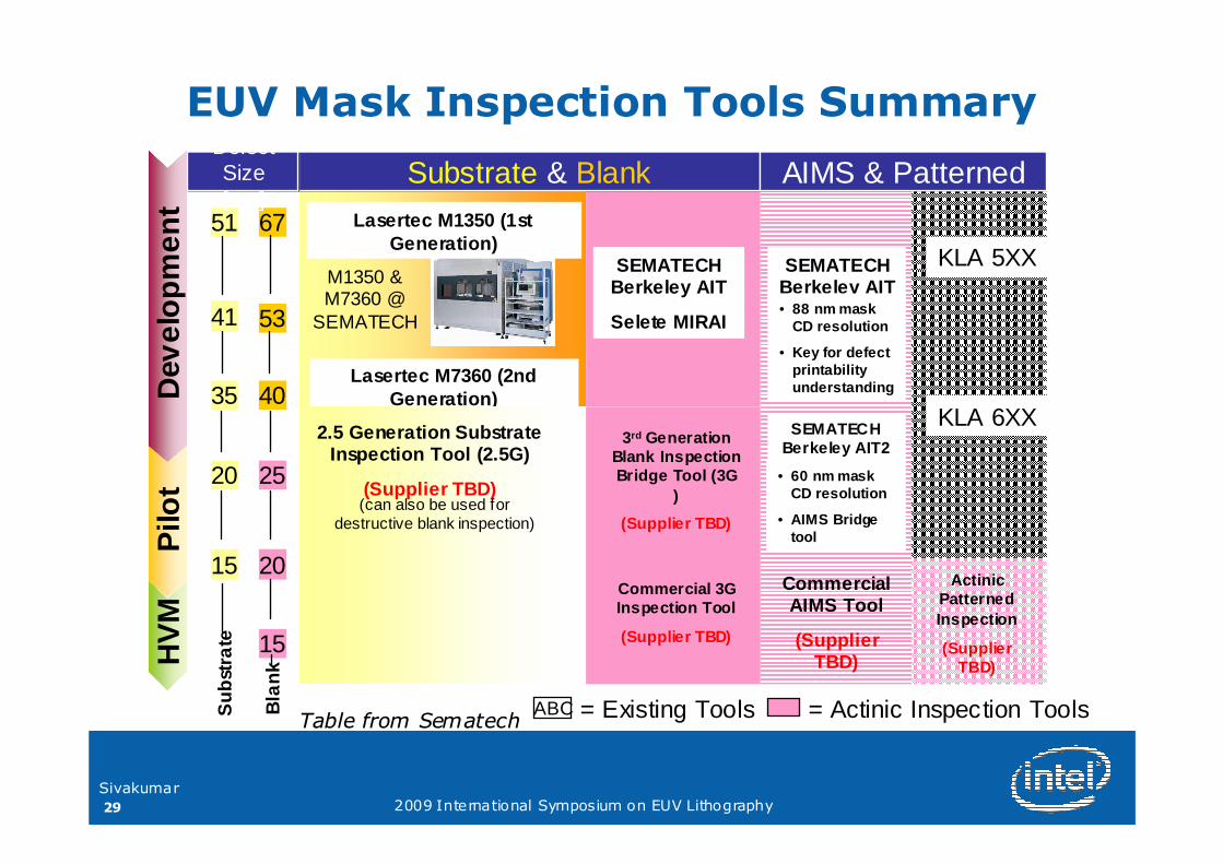
EUV Mask Inspection Tools Summary
Lasertec M7360 (2nd Generation)
Lasertec M1350 (1st Generation)
SEMATECH Berkeley AIT
Selete MIRAI
SEMATECH Berkeley AIT
51 67
Substrate & Blank AIMS & Patterned
Commercial AIMS Tool
(Supplier TBD)
3rd Generation Blank Inspection Bridge Tool (3G
)
(Supplier TBD)
2.5 Generation Substrate Inspection Tool (2.5G)
(Supplier TBD)
5341
4035
20
15
25
20
Defect Size [nm]
Pilo
tH
VM
Dev
elo
pm
ent
15
Commercial 3G Inspection Tool
(Supplier TBD)
Actinic Patterned Inspection
(Supplier TBD)
KLA 5XX
KLA 6XX
(can also be used for destructive blank inspection)
Su
bst
rate
Bla
nk
= Actinic Inspection ToolsABC = Existing Tools
M1350 & M7360 @
SEMATECH • 88 nm mask
CD resolution
• Key for defect printability understanding
SEMATECH Berkeley AIT2
• 60 nm mask CD resolution
• AIMS Bridge tool
Table from Table from SematechSematech
30
Sivakumar2009 International Symposium on EUV Lithography
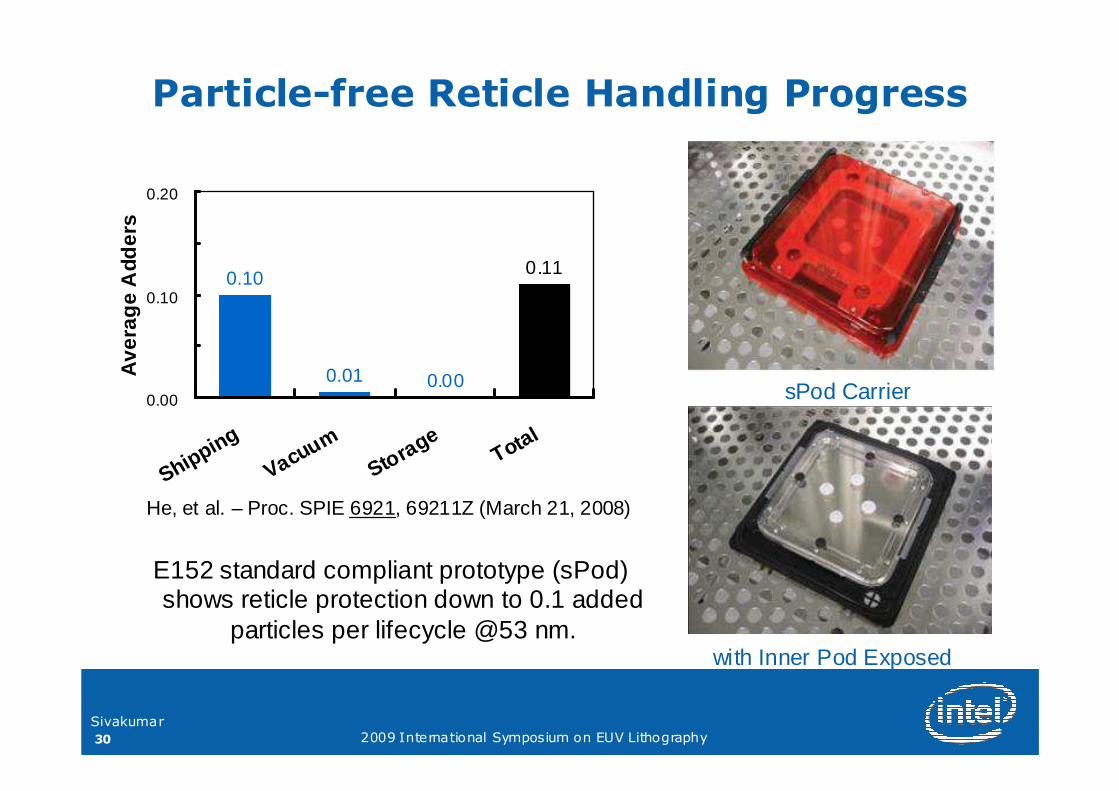
Particle-free Reticle Handling Progress
0.11
0.000.01
0.10
0.00
0.10
0.20
Shipping
VacuumStorage
Total
Ave
rag
e A
dder
s
with Inner Pod Exposed
sPod Carrier
E152 standard compliant prototype (sPod) shows reticle protection down to 0.1 added
particles per lifecycle @53 nm.
He, et al. – Proc. SPIE 6921, 69211Z (March 21, 2008)

31
Sivakumar2009 International Symposium on EUV Lithography
In-situ Inspection
� Need to verify reticle cleanliness AFTER loading into scanner and BEFORE printing wafers
– Repeater concern is serious due to lack of pellicles
– ArF scanners have in-situ reticle inspection capability
� Not having in-situ capability would require printing of defect look-ahead wafers
– Manageable in development and perhaps in pilot line mode
– Unacceptable for HVM
� Need focus from tool vendors to have capability avaialable in HVM tooling platforms

32
Sivakumar2009 International Symposium on EUV Lithography
Reticle Technical and Infrastructure Gaps
� Current reticle defectivity gap is about 25-100X
– Need continuous improvement
– Relaxation of flatness spec might help bridge gap
� Inspection gaps
– Actinic blank inspection
– Patterned defect inspection spec vs. actual
– In-situ inspection
– AIMs inspection
� SEMATECH is adopting a “bridge” tool solution for actinic blank and AIMS inspection so that some capability will be available for “pilot line” in 2011
� Production actinic inspection, AIMS, and patterned inspection will require industry-wide funding (July workshop)

33
Sivakumar2009 International Symposium on EUV Lithography
Summing Up
34
Sivakumar2009 International Symposium on EUV Lithography
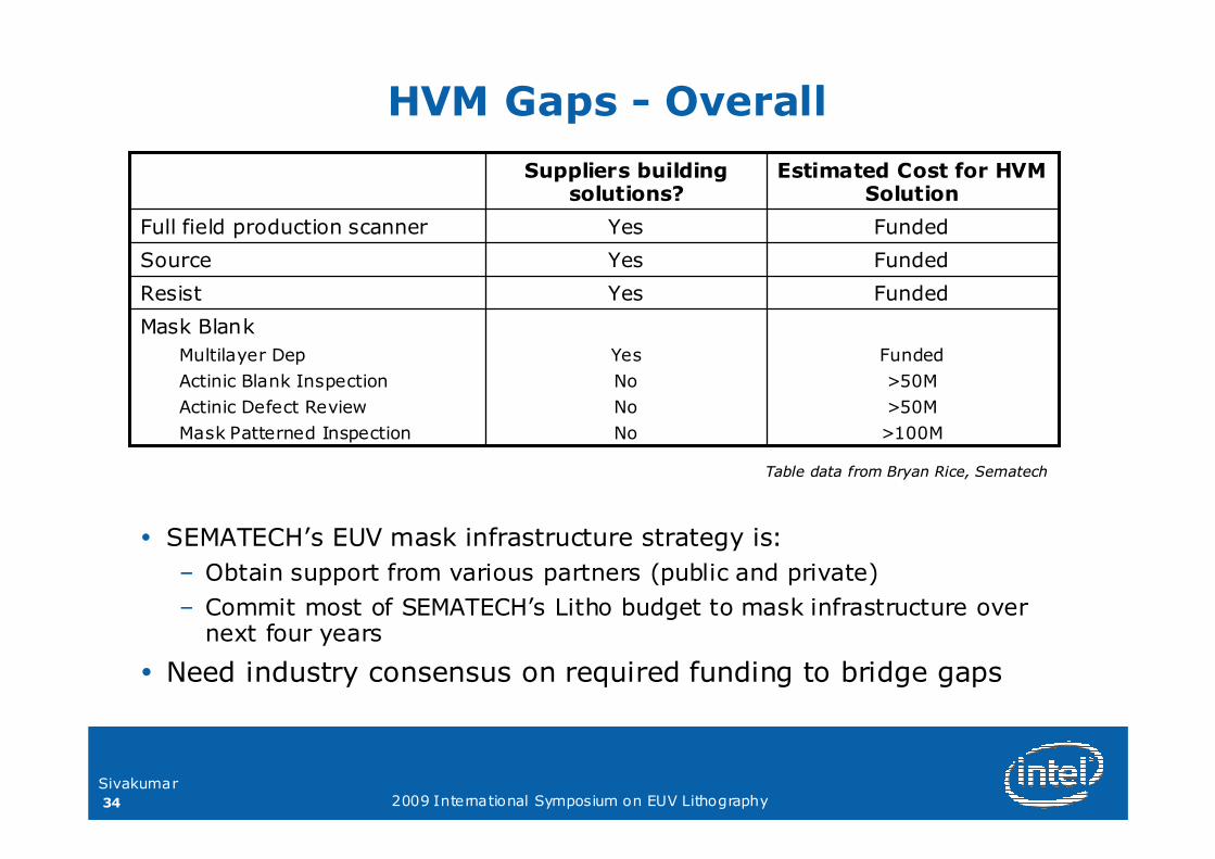
HVM Gaps - Overall
Funded
>50M
>50M
>100M
Yes
No
No
No
Mask Blank
Multilayer Dep
Actinic Blank Inspection
Actinic Defect Review
Mask Patterned Inspection
FundedYesResist
FundedYesSource
FundedYesFull field production scanner
Estimated Cost for HVM Solution
Suppliers building solutions?
� SEMATECH’s EUV mask infrastructure strategy is:
– Obtain support from various partners (public and private)
– Commit most of SEMATECH’s Litho budget to mask infrastructure over next four years
� Need industry consensus on required funding to bridge gaps
Table data from Bryan Rice, Table data from Bryan Rice, SematechSematech
35
Sivakumar2009 International Symposium on EUV Lithography
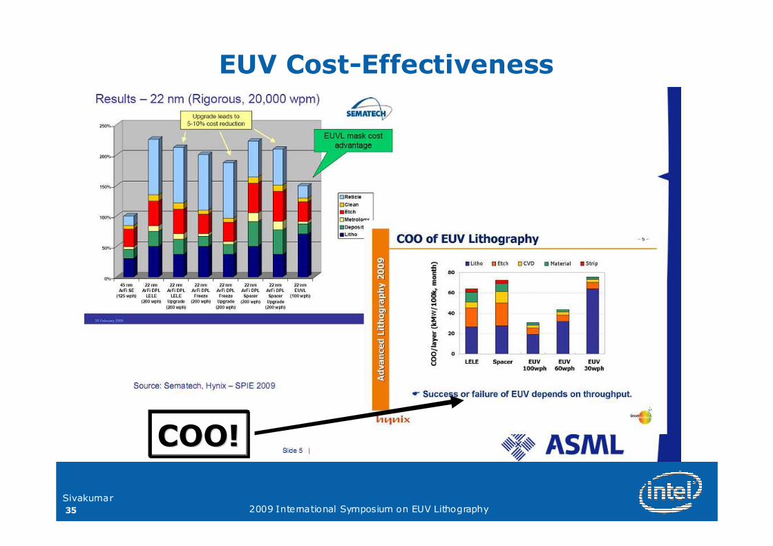
EUV Cost-Effectiveness
COO!COO!

36
Sivakumar2009 International Symposium on EUV Lithography
Conclusions
� Substantial progress made on resist and tooling
– Resists typically about 2X from goal for sensitivity/LWR
– Laser power about 10X from goal
– Overall tool runrate requires ~ 20X improvement to 100wph goal
� Reticle defectivity is a major concern
– Blank defectivity needs substantial improvement
– Relaxation of flatness requirement might provide some mitigation
– Reticle inspection capability has major gaps. Need industry funding to enable tooling to be developed in time for HVM
� Academic exercise is over!!
– EUV has moved from research to implementation mode
– Problems left to be solved are largely engineering in nature
– Need sustained focus and industry-wide commitment to solve
� Ultimately EUV insertion will be based on a COO decision vs. ArF
37
Sivakumar2009 International Symposium on EUV Lithography
Def
ect D
ensi
ty (
Log
Sca
le)
Def
ect D
ensi
ty (
Log
Sca
le)
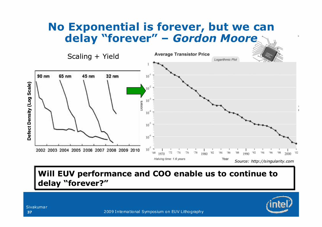
No Exponential is forever, but we can delay “forever” – Gordon Moore
Source: http://Source: http://singularity.comsingularity.com
Will EUV performance and COO enable us to continue to Will EUV performance and COO enable us to continue to
delay delay ““forever?forever?””
Scaling + YieldScaling + Yield