EsB DetectionLow Voltage – BSE Imaging - IPT Online
2
objective lens collects BSEs scattered under very low angle (almost parallel to the sample surface) and produces high quality material contrast images. Low Voltage BSE Imaging – EsB Detection In order to detect high angle BSEs (almost perpendicular to the sample surface) backing up through the lens, a new de- tector has been developed and introduced in the new ULTRA FESEM (Fig. 1). To understand the basic principle of this new detection system a closer exami- nation of the energy spectra as well as the take-off angle distributions of the re- leased electrons and their trajectories through the electron column is necessary. Fig. 4 illustrates a schematic energy Nanotechnology has become a very active and highly charged discipline in science and technology, growing rapidly in indu- strial sectors and is part of almost every field of research and engineering. The intense interest in nanotechnology is being driven by visions of a stream of new nanotech commercial applications that will dominate future industrial appea- rance. Our latest FESEM technology enables, not only routine inspection and failure analysis, but also ultra high resolu- tion imaging including the complete variety of state-of-the-art analytical featu- res essential in nanotechnology research. The GEMINI ® Column Zeiss´ Field Emission Scanning Electron Microscopes are all based on the GEMINI ® principle. In order to reduce aberrations and sensitivity to interfering strayfields the electron optical column possesses a positively biased booster that shifts the energy of the primary electrons. The inci- dent beam is focussed by a combination of a magnetic lens with an axial gap that avoids field leakage to the specimen and an electrostatic retarding lens formed by the beam booster, together with the grounded pole piece cap. Shortly before the electrons hit the specimen they are decelerated to the desired primary energy. A suitable explanation for the reduction of EsB Detection Low Voltage – BSE Imaging Dr. M. Steigerwald, Carl Zeiss SMT - Nano Technology Systems Division, 73447 Oberkochen, Germany spherical and chromatic aberrations is that the electron beam is focussed by the objective lens at higher energies and smaller electron beam diameters. The GEMINI ® concept has overcome the problem with classical objective lens designs, which immerse the specimen in the magnetic field prohibiting imaging of magnetic samples. Detection System GEMINI ® FESEMs microscopes enable a large variety of detector types (Fig. 3) to analyse all scattering products emerging from the specimen: Secondary electrons (SEs) used mostly to resolve topographic and charging information, backscattered electrons (BSEs) to enhance compositional contrast and crystal orientation, as well as photons to visualise lattice structures or to show luminescence effects. Beside the already mentioned benefits of highest resolution and beam stability, the beam booster is also advantageous for secondary electron collection. SEs emerging from the sample surface are attracted and accelerated by the posi- tively biased electrode of the beam booster and are collected with the SE In- lens detector. An additional Everhart- Thornley chamber detector (ETD) collects remaining SEs that are not captured by the beam booster (especially at large wor- king distances) or second generation secondary electrons, SE3 type, which are produced by BSE interaction with the objective lens. The ETD typically depicts compositionally enhanced contrast combined with some surface information. Correct BSE detection is rather complicated and needs several detectors covering the whole solid angle depending on the primary energy of the initial electrons. A retractable quadrant diode detector installed beneath the Fig. 2: GEMINI ® bias concept Fig. 3: GEMINI ® detectors Fig. 1: The ULTRA FESEM
Transcript of EsB DetectionLow Voltage – BSE Imaging - IPT Online

objective lens collects BSEs scattered
under very low angle (almost parallel to
the sample surface) and produces high
quality material contrast images.
Low Voltage BSEImaging – EsBDetectionIn order to detect high angle BSEs (almost
perpendicular to the sample surface)
backing up through the lens, a new de-
tector has been developed and introduced
in the new ULTRA FESEM (Fig. 1).
To understand the basic principle of
this new detection system a closer exami-
nation of the energy spectra as well as the
take-off angle distributions of the re-
leased electrons and their trajectories
through the electron column is necessary.
Fig. 4 illustrates a schematic energy
Nanotechnology has become a very active
and highly charged discipline in science
and technology, growing rapidly in indu-
strial sectors and is part of almost every
field of research and engineering. The
intense interest in nanotechnology is
being driven by visions of a stream of new
nanotech commercial applications that
will dominate future industrial appea-
rance. Our latest FESEM technology
enables, not only routine inspection and
failure analysis, but also ultra high resolu-
tion imaging including the complete
variety of state-of-the-art analytical featu-
res essential in nanotechnology research.
The GEMINI® ColumnZeiss´ Field Emission Scanning Electron
Microscopes are all based on the GEMINI®
principle. In order to reduce aberrations
and sensitivity to interfering strayfields
the electron optical column possesses a
positively biased booster that shifts the
energy of the primary electrons. The inci-
dent beam is focussed by a combination
of a magnetic lens with an axial gap that
avoids field leakage to the specimen and
an electrostatic retarding lens formed by
the beam booster, together with the
grounded pole piece cap. Shortly before
the electrons hit the specimen they are
decelerated to the desired primary energy.
A suitable explanation for the reduction of
EsB Detection Low Voltage – BSE Imaging Dr. M. Steigerwald, Carl Zeiss SMT - Nano Technology Systems Division, 73447 Oberkochen, Germany
spherical and chromatic aberrations is
that the electron beam is focussed by the
objective lens at higher energies and
smaller electron beam diameters. The
GEMINI® concept has overcome the
problem with classical objective lens
designs, which immerse the specimen in
the magnetic field prohibiting imaging of
magnetic samples.
Detection SystemGEMINI® FESEMs microscopes enable a
large variety of detector types (Fig. 3) to
analyse all scattering products emerging
from the specimen: Secondary electrons
(SEs) used mostly to resolve topographic
and charging information, backscattered
electrons (BSEs) to enhance compositional
contrast and crystal orientation, as well as
photons to visualise lattice structures or
to show luminescence effects.
Beside the already mentioned benefits of
highest resolution and beam stability,
the beam booster is also advantageous
for secondary electron collection. SEs
emerging from the sample surface are
attracted and accelerated by the posi-
tively biased electrode of the beam
booster and are collected with the SE In-
lens detector. An additional Everhart-
Thornley chamber detector (ETD) collects
remaining SEs that are not captured by
the beam booster (especially at large wor-
king distances) or second generation
secondary electrons, SE3 type, which are
produced by BSE interaction with the
objective lens.
The ETD typically depicts compositionally
enhanced contrast combined with some
surface information. Correct BSE detection
is rather complicated and needs several
detectors covering the whole solid angle
depending on the primary energy of the
initial electrons. A retractable quadrant
diode detector installed beneath the
Fig. 2: GEMINI® bias concept
Fig. 3: GEMINI® detectors
����������
�� ����������
����������������
������������������
���������������������
�� ��������������������
�������������������������� �� ���������
�������������������
�����������������
Fig. 1: The ULTRA FESEM !
�
��
�" �#�
!���������
������� ���������#������ �
$��#�������������
$��#������������
�����%���
�� ����������
���������
����������������
��������
Beside electron energy level, both electron
types also differ in respect to their take-
off angle distribution. While the distribu-
tion of secondary electrons orientates
perpendicularly to topographic structures,
backscattered electrons emerge from the
bulk material and are therefore less sensi-
tive to surface topography.
Emerging from the specimen surface most
of the electrons are attracted by the beam
booster and move upstream into the
GEMINI® column. Because of the chroma-
tic aberation of the magnetic lens the
electrons are forced on different trajecto-
ries depending on their energy when
traversing the focus-
sing field. Both, the
deflection of the lens
and the different take-
off angle distribution
result in different phase
spaces at the position
of the lower annular
In-lens SE detector (Fig.
5). The green ellipse
indicates SEs posses-
sing large divergence
!������ ��
����������� ������������
����������������
����������
�� ���
spectrum of electrons escaping from the
specimen. Secondary electrons (green),
possessing very low energies by defini-
tion, are released near the surface and
produce a signal rich in topographic infor-
mation, where as backscattered electrons
(blue), which have undergone at least one
large angle scattering, originate from lar-
ger depths and possess compositional
information.
Fig. 5: Phase space comparison
Fig. 6: Radial electron distribution
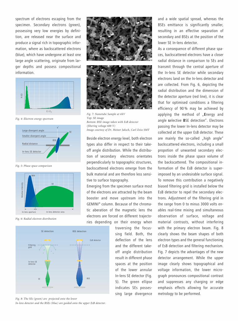
Fig. 7: Nanotube Sample at 4 kV
Top: SE image
Bottom: BSE image taken with EsB detector
(filtering voltage 600 V)
Image courtesy of Dr. Heiner Jaksch, Carl Zeiss SMT
�����������������
���
��
&��������������
����������� ������ ��
'� ������ ������ ��"(
������������#� ������������������
&�����������������
���
��
and a wide spatial spread, whereas the
BSEs emittance is significantly smaller,
resulting in an effective separation of
secondary and BSEs at the position of the
lower SE In-lens detector.
As a consequence of different phase spa-
ces, backscattered electrons have a closer
radial distance in comparison to SEs and
transmit through the central aperture of
the In-lens SE detector while secondary
electrons land on the In-lens detector and
are collected. From Fig. 6, depicting the
radial distribution and the dimension of
the detector aperture (red line), it is clear
that for optimised conditions a filtering
efficiency of 90 % may be achieved by
applying the method of „Energy and
angle selective BSE detection“. Electrons
passing the lower In-lens detector may be
collected at the upper EsB detector. These
are mainly the so-called „high angle“
backscattered electrons, including a small
propotion of unwanted secondary elec-
trons inside the phase space volume of
the backscattered. The compositional in-
formation of the EsB detector is super-
imposed by an undesirable surface signal.
To remove this contribution a negatively
biased filtering grid is installed below the
EsB detector to repel the secondary elec-
trons. Adjustment of the filtering grid in
the range from 0 to minus 3000 volts en-
ables real-time mixing and simultaneous
observation of surface, voltage and
material contrasts, without interfering
with the primary electron beam. Fig. 8
clearly shows the beam shapes of both
electron types and the general functioning
of EsB detection and filtering mechanism.
Fig. 7 depicts the advantages of the new
detector arrangement. While the upper
image clearly shows topographical and
voltage information, the lower micro-
graph pronounces compositional contrast
and suppresses any charging or edge
emphasis effects allowing for accurate
metrology to be performed.Fig. 8: The SEs (green) are projected onto the lower
In-lens detector and the BSEs (blue) are guided onto the upper EsB detector.
Fig. 4: Electron energy spectrum
)�*�+
��,��