Ericsson Internal PRODUCT SPECIFICATION TABLE …...Ericsson Internal PRODUCT SPECIFICATION 1 (4)...
28
PRODUCT SPECIFICATION 1 (4) Prepared (also subject responsible if other) No. Kevin Zhou 1/1301-BMR 451 Uen Approved Checked Date Rev Reference Kevin Zhou 2017-10-12 H Key Features • Small package 30.85 x 20 x 8.2 mm (1.215 x 0.787 x 0.323 in.) • 40 A output current • 4.5 V – 14 V input voltage range • 0.6 V – 3.6 V output voltage range (by PMBus) • 0.7 V – 3.3 V output voltage range (by external resistor) • High efficiency, typ. 96,4% at half load, 5 Vin, 3.3 Vout • 6.9 million hours MTBF • Through hole and surface mount versions • PMBus read and write compliant General Characteristics • Voltage/current/temperature monitoring • Precision delay and ramp-up • Voltage sequencing • Switching frequency synchronization • Configurable control loop • Non-linear transient response • Wide output voltage adjust function • Start up into a pre-biased output • Output short-circuit protection • Over temperature protection • On/Off remote control • Output voltage sense • ISO 9001/14001 certified supplier Safety Approvals Design for Environment Meets requirements in high- temperature lead-free soldering processes. Ericsson Internal TABLE OF CONTENTS 1 (1) Prepared (also subject responsible if other) No. EZIWSON 001 52 - EN/LZT 146 401 Uen Approved Checked Date Rev Reference SEC/D (Julia You) 2011-08-11 E D Contents Ordering Information ............................................................. 2 General Information ............................................................. 2 Safety Specification ............................................................. 3 Absolute Maximum Ratings ............................................................. 4 Functional Specification ............................................................. 5 Electrical Specification 1.0V, 40A / 40W BMR 451 0002/020............................... 6 3.3V, 40A / 132W BMR 451 0002/020............................... 9 EMC Specification ........................................................... 12 Operating Information ........................................................... 12 Thermal Consideration ........................................................... 16 Connections ........................................................... 17 Typical Application Circuits ........................................................... 17 PMbus Interface & Commands ........................................................... 18 Mechanical Information ........................................................... 21 Soldering Information ........................................................... 24 Delivery Information ........................................................... 25 Product Qualification Specification ........................................................... 28 BMR 451 Digital PoL Regulators Input 4.5 - 14 V, Output up to 40 A / 132 W EN/LZT 146 401 R5A October 2017 © Flex Technical Specification
Transcript of Ericsson Internal PRODUCT SPECIFICATION TABLE …...Ericsson Internal PRODUCT SPECIFICATION 1 (4)...
PRODUCT SPECIFICATION
1 (4)
Prepared (also subject responsible if other) No.
Kevin Zhou 1/1301-BMR 451 Uen Approved Checked Date Rev Reference
Kevin Zhou 2017-10-12 H
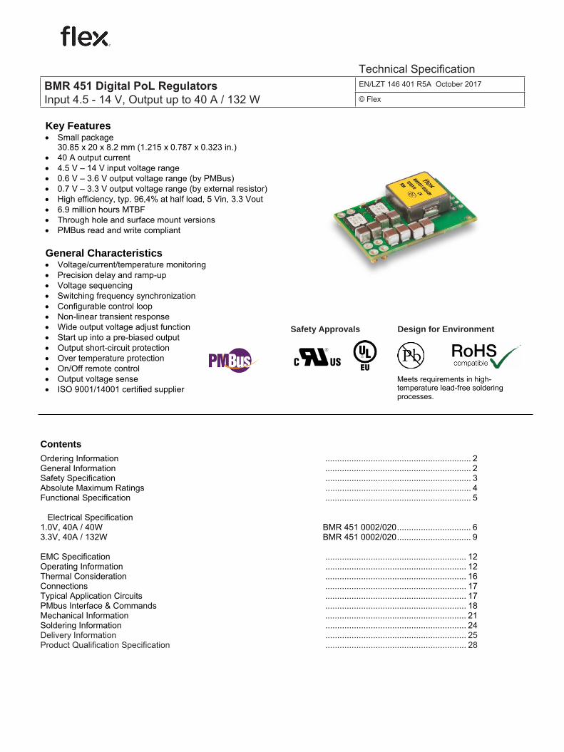
Key Features • Small package
30.85 x 20 x 8.2 mm (1.215 x 0.787 x 0.323 in.) • 40 A output current • 4.5 V – 14 V input voltage range • 0.6 V – 3.6 V output voltage range (by PMBus) • 0.7 V – 3.3 V output voltage range (by external resistor) • High efficiency, typ. 96,4% at half load, 5 Vin, 3.3 Vout • 6.9 million hours MTBF • Through hole and surface mount versions • PMBus read and write compliant General Characteristics • Voltage/current/temperature monitoring • Precision delay and ramp-up • Voltage sequencing • Switching frequency synchronization • Configurable control loop • Non-linear transient response • Wide output voltage adjust function • Start up into a pre-biased output • Output short-circuit protection • Over temperature protection • On/Off remote control • Output voltage sense • ISO 9001/14001 certified supplier
Safety Approvals Design for Environment
Meets requirements in high-
temperature lead-free soldering processes.
Ericsson Internal TABLE OF CONTENTS 1 (1)
Prepared (also subject responsible if other) No.
EZIWSON 001 52 - EN/LZT 146 401 Uen Approved Checked Date Rev Reference
SEC/D (Julia You) 2011-08-11 E D
Contents
Ordering Information ............................................................. 2 General Information ............................................................. 2 Safety Specification ............................................................. 3 Absolute Maximum Ratings ............................................................. 4 Functional Specification ............................................................. 5 Electrical Specification 1.0V, 40A / 40W BMR 451 0002/020............................... 6 3.3V, 40A / 132W BMR 451 0002/020............................... 9 EMC Specification ........................................................... 12 Operating Information ........................................................... 12 Thermal Consideration ........................................................... 16 Connections ........................................................... 17 Typical Application Circuits ........................................................... 17 PMbus Interface & Commands ........................................................... 18 Mechanical Information ........................................................... 21 Soldering Information ........................................................... 24 Delivery Information ........................................................... 25 Product Qualification Specification ........................................................... 28
BMR 451 Digital PoL RegulatorsInput 4.5 - 14 V, Output up to 40 A / 132 W
EN/LZT 146 401 R5A October 2017
© Flex
Technical Specification
Ordering Information
Product program Output BMR451 0.6 - 3.6 V / 40 A, 132 W Product number and Packaging BMR 451 n1n2n3n4/n5n6n7n8 Options n1 n2 n3 n4 / n5 n6 n7 n8 Mounting / Mechanical / Digital interface / Configuration file / Packaging / Optional designation Description n1
n2
n3 n4 n5 n6 n7 n8
0 = Through hole mounted version (TH) 1 = Surface mount version (SMD) 0 = lead length 3.56mm * 4 = lead length 3mm and pin in paste option * 02 = PMBus and analog voltage adjust 020 = Standard configuration xxx = Application Specific Configuration B = Antistatic injection molded tray of 30 products (5 full trays/box = 150 products) C = Antistatic tape & reel of 130 products
Example: Product number BMR4511002/020 equals a surface mount, open frame, PMBus and analog voltage adjust, standard configuration variant. For application specific configurations contact your local Flex sales representative. *Note: only applicable for through hole mounted version. General Information Reliability
The failure rate () and mean time between failures (MTBF= 1/) is calculated at max output power and an operating ambient temperature (TA) of +40°C. Flex uses Telcordia SR-332 Issue 2 Method 1 to calculate the mean steady-state failure rate and standard deviation (). Telcordia SR-332 Issue 2 also provides techniques to estimate the upper confidence levels of failure rates based on the mean and standard deviation.
Mean steady-state failure rate, Std. deviation,
146 nFailures/h 38.3 nFailures/h MTBF (mean value) for the BMR451 series = 6.9 Mh. MTBF at 90% confidence level = 5.1 Mh
Compatibility with RoHS requirements The products are compatible with the relevant clauses and requirements of the RoHS directive 2002/95/EC and have a maximum concentration value of 0.1% by weight in homogeneous materials for lead, mercury, hexavalent chromium, PBB and PBDE and of 0.01% by weight in homogeneous materials for cadmium. Exemptions in the RoHS directive utilized in Flex products include: - Lead in high melting temperature type solder (used to
solder the die in semiconductor packages) - Lead in glass of electronics components and in
electronic ceramic parts (e.g. fill material in chip resistors)
- Lead as an alloying element in copper alloy containing up to 4% lead by weight (used in connection pins made of Brass)
Quality Statement The products are designed and manufactured in an industrial environment where quality systems and methods like ISO 9000, 6σ (sigma), and SPC are intensively in use to boost the continuous improvements strategy. Infant mortality or early failures in the products are screened out and they are subjected to an ATE-based final test. Conservative design rules, design reviews and product qualifications, plus the high competence of an engaged work force, contribute to the high quality of our products. Warranty
Warranty period and conditions are defined in Flex’s General Terms and Conditions of Sale. Flex does not make any other warranties, expressed or implied including any warranty of merchantability, effects of product configurations made by customers or fitness for a particular purpose.
© Flex 2017
The information and specifications in this technical specification is believed to be correct at the time of publication. However, no liability is accepted for inaccuracies, printing errors or for any consequences thereof. Flex reserves the right to change the contents of this technical specification at any time without prior notice.
BMR 451 Digital PoL RegulatorsInput 4.5 - 14 V, Output up to 40 A / 132 W
EN/LZT 146 401 R5A October 2017
© Flex
Technical Specification 2
Safety Specification
General information
Flex DC/DC converters and DC/DC regulators are designed in accordance with safety standards IEC/EN/UL 60950-1 Safety of Information Technology Equipment. IEC/EN/UL 60950-1 contains requirements to prevent injury or damage due to the following hazards:
• Electrical shock • Energy hazards • Fire • Mechanical and heat hazards • Radiation hazards • Chemical hazards
On-board DC/DC converters and DC/DC regulators are defined as component power supplies. As components they cannot fully comply with the provisions of any safety requirements without “Conditions of Acceptability”. Clearance between conductors and between conductive parts of the component power supply and conductors on the board in the final product must meet the applicable safety requirements. Certain conditions of acceptability apply for component power supplies with limited stand-off (see Mechanical Information for further information). It is the responsibility of the installer to ensure that the final product housing these components complies with the requirements of all applicable safety standards and regulations for the final product. Component power supplies for general use should comply with the requirements in IEC 60950-1, EN 60950-1 and UL 60950-1 Safety of Information Technology Equipment. There are other more product related standards, e.g. IEEE 802.3 CSMA/CD (Ethernet) Access Method, and ETS-300132-2 Power supply interface at the input to telecommunications equipment, operated by direct current (dc), but all of these standards are based on IEC/EN/UL 60950-1 with regards to safety. Flex DC/DC converters and DC/DC regulators are UL 60950-1 recognized and certified in accordance with EN 60950-1. The flammability rating for all construction parts of the products meet requirements for V-0 class material according to IEC 60695-11-10, Fire hazard testing, test flames – 50 W horizontal and vertical flame test methods. The products should be installed in the end-use equipment, in accordance with the requirements of the ultimate application. Normally the output of the DC/DC converter is considered as SELV (Safety Extra Low Voltage) and the input source must be isolated by minimum Double or Reinforced Insulation from the primary circuit (AC mains) in accordance with IEC/EN/UL 60950-1.
Isolated DC/DC converters It is recommended that a slow blow fuse is to be used at the input of each DC/DC converter. If an input filter is used in the circuit the fuse should be placed in front of the input filter. In the rare event of a component problem that imposes a short circuit on the input source, this fuse will provide the following functions:
• Isolate the fault from the input power source so as not to affect the operation of other parts of the system.
• Protect the distribution wiring from excessive current and power loss thus preventing hazardous overheating.
The galvanic isolation is verified in an electric strength test. The test voltage (Viso) between input and output is 1500 Vdc or 2250 Vdc (refer to product specification). 24 V DC systems
The input voltage to the DC/DC converter is SELV (Safety Extra Low Voltage) and the output remains SELV under normal and abnormal operating conditions. 48 and 60 V DC systems If the input voltage to the DC/DC converter is 75 Vdc or less, then the output remains SELV (Safety Extra Low Voltage) under normal and abnormal operating conditions. Single fault testing in the input power supply circuit should be performed with the DC/DC converter connected to demonstrate that the input voltage does not exceed 75 Vdc. If the input power source circuit is a DC power system, the source may be treated as a TNV-2 circuit and testing has demonstrated compliance with SELV limits in accordance with IEC/EN/UL60950-1. Non-isolated DC/DC regulators
The input voltage to the DC/DC regulator is SELV (Safety Extra Low Voltage) and the output remains SELV under normal and abnormal operating conditions.
BMR 451 Digital PoL RegulatorsInput 4.5 - 14 V, Output up to 40 A / 132 W
EN/LZT 146 401 R5A October 2017
© Flex
Technical Specification 3
Ericsson Internal PRODUCT SPEC 1 (9)
Prepared (also subject responsible if other) No.
ETORHOL, EKAMAGN, EJANARV 2/1301-BMR 451 0002 Uen Approved Checked Date Rev Reference
SEC/D (Julia You) ETORHOL 2010-03-02 E
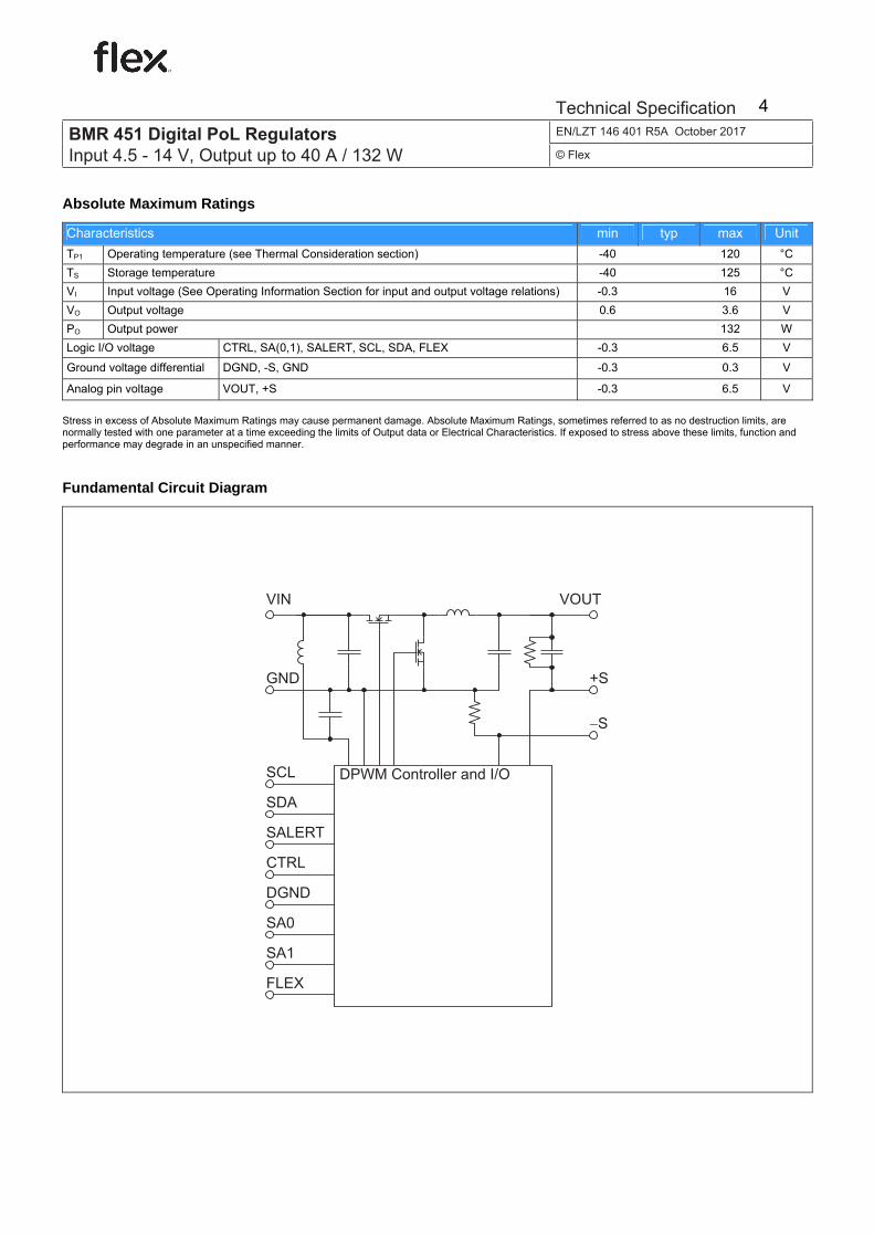
Absolute Maximum Ratings
Characteristics min typ max Unit TP1 Operating temperature (see Thermal Consideration section) -40 120 °C TS Storage temperature -40 125 °C VI Input voltage (See Operating Information Section for input and output voltage relations) -0.3 16 V VO Output voltage 0.6 3.6 V PO Output power 132 W Logic I/O voltage CTRL, SA(0,1), SALERT, SCL, SDA, FLEX -0.3 6.5 V
Ground voltage differential DGND, -S, GND -0.3 0.3 V
Analog pin voltage VOUT, +S -0.3 6.5 V
Stress in excess of Absolute Maximum Ratings may cause permanent damage. Absolute Maximum Ratings, sometimes referred to as no destruction limits, are normally tested with one parameter at a time exceeding the limits of Output data or Electrical Characteristics. If exposed to stress above these limits, function and performance may degrade in an unspecified manner.
Fundamental Circuit Diagram
BMR 451 Digital PoL RegulatorsInput 4.5 - 14 V, Output up to 40 A / 132 W
EN/LZT 146 401 R5A October 2017
© Flex
Technical Specification 4
Ericsson Internal PRODUCT SPEC 2 (9)
Prepared (also subject responsible if other) No.
ETORHOL, EKAMAGN, EJANARV 2/1301-BMR 451 0002 Uen Approved Checked Date Rev Reference
SEC/D (Julia You) ETORHOL 2010-03-02 E
Functional Specification
TP1 = -40 to +85ºC, VI = 4.5 to 14 V Typical values given at: TP1 = +25°C, VI = 12 V, max IO, unless otherwise specified under Conditions Configuration File: 190 10-CDA 102 900/020 Characteristics Conditions min typ max Unit
SMBus monitoring VIN_READ, 0x88h Accuracy vs. VI -3 3 % VOUT_READ, 0x8Bh Accuracy vs. VO -1 1 % IOUT_READ, 0x8Ch Accuracy vs. IO -20 20 %
General Electrical Characteristics fs Switching frequency Factory default 320 kHz CISMBus Internal capacitance SMBus signals, SDA, SCL 10 pF
CI Internal input capacitance 140 µF Fault Protection Characteristics
UVLO Threshold 4.0 V Set point accuracy -100 100 mV Hysteresis Factory default 0.4 V
Input Under Voltage Lockout, UVLO
Delay 2.5 µs UVP threshold Factory default 85 % VOUT OVP threshold Factory default 115 % VOUT
(Output voltage) Over/Under Voltage Protection, OVP/UVP OVP/UVP fault response
time Factory default 25 µs
Set point accuracy Io -20 +20 % OCP threshold Factory default 50 A
Over Current Protection, OCP OCP protection delay Factory default 45 µs
OTP threshold Factory default 120 Over Temperature Protection, OTP at TP1 OTP hysteresis Factory default 15
°C
Logic Input/Output Characteristics Logic input low threshold (VIL) 0.8 V
Logic input high threshold (VIH) CTRL, SCL, SDA, FLEX
2.0 V
Logic output low (VOL) SALERT, SCL, SDA, FLEX IOL ≤ 4 mA 0.4 V
Logic output high (VOH) SALERT, SCL, SDA, FLEX IOL ≥ -2 mA 2.25 V
Setup time, SMBus (tset) See Note 1 300 ns
Hold time, SMBus (thold) See Note 1 250 ns
Note 1: See operation information section for I2C/SMBus Setup and Hold Times – Definitions
BMR 451 Digital PoL RegulatorsInput 4.5 - 14 V, Output up to 40 A / 132 W
EN/LZT 146 401 R5A October 2017
© Flex
Technical Specification 5
Ericsson Internal PRODUCT SPEC 3 (9)
Prepared (also subject responsible if other) No.
ETORHOL, EKAMAGN, EJANARV 2/1301-BMR 451 0002 Uen Approved Checked Date Rev Reference
SEC/D (Julia You) ETORHOL 2010-03-02 E
1.0 V, 40 A/40 W Electrical Specification BMR 451 0002/020
TP1 = -40 to +85ºC, VI = 4.5 to 14 V. Configuration: CDA 102 900/020, RSET = 19.6 kΩ. Typical values given at: TP1 = +25°C, VI = 12.0 V, max IO, unless otherwise specified under Conditions. Additional CI = 470 µF. See Operating Information section for selection of capacitor types. Sense pins are connected to the output pins. Characteristics Conditions min typ max Unit
VI Input voltage range 4.5 14 V VIoff Turn-off input voltage Decreasing input voltage 4.0 V VIon Turn-on input voltage Increasing input voltage 4.4 V PO Output power 40 W
50 % of max IO 89.1 η Efficiency
max IO 86.5 %
Pd Power dissipation 6.2 W Pli Input idling power IO = 0.01 A 0.9 W
Turned off with CTRL, monitoring enabled, see Note 3 145 mW
PRC Input standby power Low power mode, monitoring disabled, see Note 3 50 mW
IS Static input current 3.9 A
VOi Output voltage initial setting and accuracy 0.990 1.000 1.010 V
Output voltage tolerance band 0.05 - 100 % of max IO 0.985 1.015 V Idling voltage IO = 0.01 A 1.000 V Line regulation 4 mV
VO
Load regulation 0.05 - 100 % of max IO 3 mV Vtr1 Load transient voltage deviation -35/+40 mV
ttr1 Load transient recovery time
Load step 25-75-25 % of max IO, di/dt = 2.5 A/µs with default configuration and CO = 10 mF. See Note 1
200 µs
CO Recommended external capacitance See Note 1 680 100 000 µF
tr Ramp-up time (from 10−90 % of VOi) 10 ms
ts Start-up time (from VI connection to 90 % of VOi)
0.05 - 100 % of max IO 37 ms
1 ms tf VO shut-down fall time (from VI off to 10 % of VO) IO = 2 A 50 ms CTRL start-up time 20 ms
7 ms tCTRL CTRL shut-down fall time (From CTRL off to 10 % of VO) IO = 2 A 17 ms
IO Output current 0.01 40 A Ilim Current limit threshold 41 48 A Isc Short circuit current 50 A VOac Output ripple & noise See Note 2 20 mVp-p
Note 1: See Operating Information section for External Decoupling Capacitors. Note 2: See Operating Information section for Output Ripple and Noise. Note 3: Configurable via PMBus, please contact your local Flex Power Modules representative for appropriate SW tools to down-load new configurations.
BMR 451 Digital PoL RegulatorsInput 4.5 - 14 V, Output up to 40 A / 132 W
EN/LZT 146 401 R5A October 2017
© Flex
Technical Specification 6
Ericsson Internal PRODUCT SPEC 4 (9)
Prepared (also subject responsible if other) No.
ETORHOL, EKAMAGN, EJANARV 2/1301-BMR 451 0002 Uen Approved Checked Date Rev Reference
SEC/D (Julia You) ETORHOL 2010-03-02 E
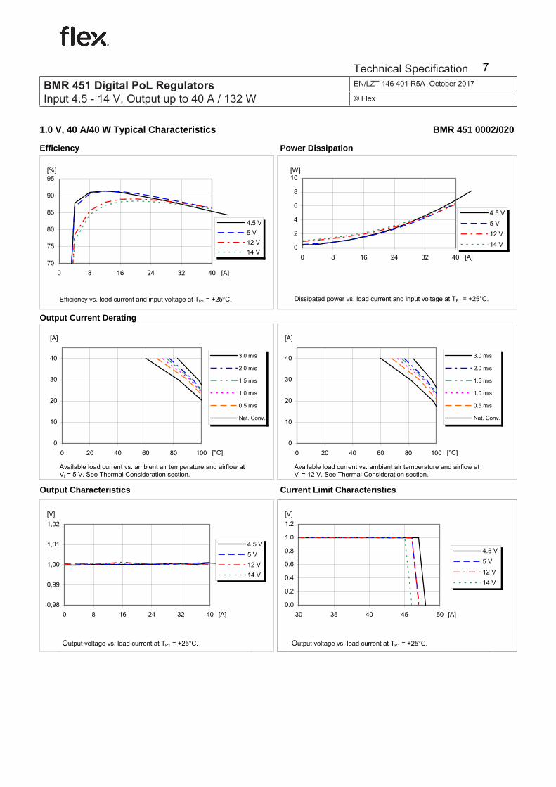
1.0 V, 40 A/40 W Typical Characteristics BMR 451 0002/020
Efficiency Power Dissipation
70
75
80
85
90
95
0 8 16 24 32 40 [A]
[%]
4.5 V5 V12 V14 V
0
2
4
6
8
10
0 8 16 24 32 40 [A]
[W]
4.5 V5 V12 V14 V
Efficiency vs. load current and input voltage at TP1 = +25°C. Dissipated power vs. load current and input voltage at TP1 = +25°C.
Output Current Derating
0
10
20
30
40
0 20 40 60 80 100 [°C]
[A]
3.0 m/s
2.0 m/s
1.5 m/s
1.0 m/s
0.5 m/s
Nat. Conv.
0
10
20
30
40
0 20 40 60 80 100 [°C]
[A]
3.0 m/s
2.0 m/s
1.5 m/s
1.0 m/s
0.5 m/s
Nat. Conv.
Available load current vs. ambient air temperature and airflow at VI = 5 V. See Thermal Consideration section.
Available load current vs. ambient air temperature and airflow at VI = 12 V. See Thermal Consideration section.
Output Characteristics Current Limit Characteristics
0,98
0,99
1,00
1,01
1,02
0 8 16 24 32 40 [A]
[V]
4.5 V5 V12 V14 V
0.0
0.2
0.4
0.6
0.8
1.0
1.2
30 35 40 45 50 [A]
[V]
4.5 V5 V12 V14 V
Output voltage vs. load current at TP1 = +25°C. Output voltage vs. load current at TP1 = +25°C.
BMR 451 Digital PoL RegulatorsInput 4.5 - 14 V, Output up to 40 A / 132 W
EN/LZT 146 401 R5A October 2017
© Flex
Technical Specification 7
Ericsson Internal PRODUCT SPEC 5 (9)
Prepared (also subject responsible if other) No.
ETORHOL, EKAMAGN, EJANARV 2/1301-BMR 451 0002 Uen Approved Checked Date Rev Reference
SEC/D (Julia You) ETORHOL 2010-03-02 E
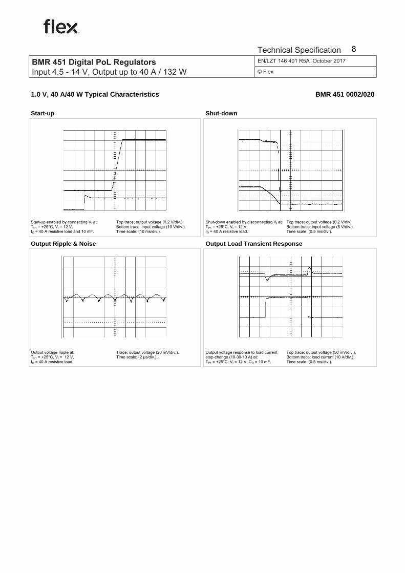
1.0 V, 40 A/40 W Typical Characteristics BMR 451 0002/020
Start-up Shut-down
Start-up enabled by connecting VI at: TP1 = +25°C, VI = 12 V, IO = 40 A resistive load and 10 mF.
Top trace: output voltage (0.2 V/div.). Bottom trace: input voltage (10 V/div.). Time scale: (10 ms/div.).
Shut-down enabled by disconnecting VI at: TP1 = +25°C, VI = 12 V, IO = 40 A resistive load.
Top trace: output voltage (0.2 V/div). Bottom trace: input voltage (5 V/div.). Time scale: (0.5 ms/div.).
Output Ripple & Noise Output Load Transient Response
Output voltage ripple at: TP1 = +25°C, VI = 12 V, IO = 40 A resistive load.
Trace: output voltage (20 mV/div.). Time scale: (2 µs/div.).
Output voltage response to load current step-change (10-30-10 A) at: TP1 = +25°C, VI = 12 V, CO = 10 mF.
Top trace: output voltage (50 mV/div.). Bottom trace: load current (10 A/div.). Time scale: (0.5 ms/div.).
BMR 451 Digital PoL RegulatorsInput 4.5 - 14 V, Output up to 40 A / 132 W
EN/LZT 146 401 R5A October 2017
© Flex
Technical Specification 8
Ericsson Internal PRODUCT SPEC 6 (9)
Prepared (also subject responsible if other) No.
ETORHOL, EKAMAGN, EJANARV 2/1301-BMR 451 0002 Uen Approved Checked Date Rev Reference
SEC/D (Julia You) ETORHOL 2010-03-02 E
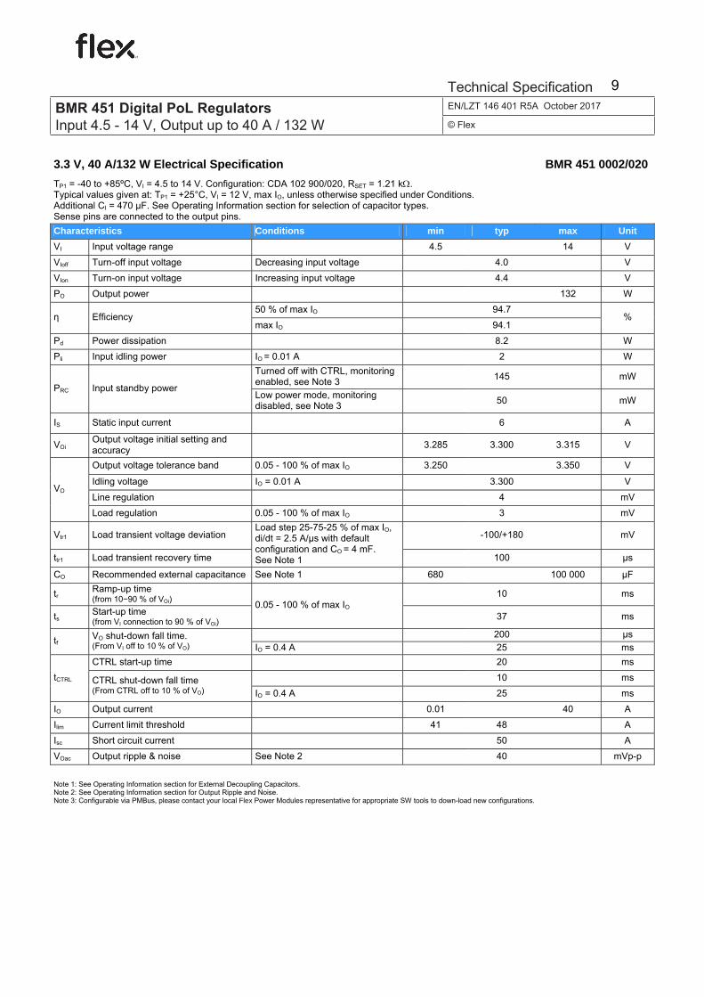
3.3 V, 40 A/132 W Electrical Specification BMR 451 0002/020
TP1 = -40 to +85ºC, VI = 4.5 to 14 V. Configuration: CDA 102 900/020, RSET = 1.21 kΩ. Typical values given at: TP1 = +25°C, VI = 12 V, max IO, unless otherwise specified under Conditions. Additional CI = 470 µF. See Operating Information section for selection of capacitor types. Sense pins are connected to the output pins. Characteristics Conditions min typ max Unit
VI Input voltage range 4.5 14 V VIoff Turn-off input voltage Decreasing input voltage 4.0 V VIon Turn-on input voltage Increasing input voltage 4.4 V PO Output power 132 W
50 % of max IO 94.7 η Efficiency
max IO 94.1 %
Pd Power dissipation 8.2 W Pli Input idling power IO = 0.01 A 2 W
Turned off with CTRL, monitoring enabled, see Note 3 145 mW
PRC Input standby power Low power mode, monitoring disabled, see Note 3 50 mW
IS Static input current 6 A
VOi Output voltage initial setting and accuracy 3.285 3.300 3.315 V
Output voltage tolerance band 0.05 - 100 % of max IO 3.250 3.350 V
Idling voltage IO = 0.01 A 3.300 V Line regulation 4 mV
VO
Load regulation 0.05 - 100 % of max IO 3 mV
Vtr1 Load transient voltage deviation -100/+180 mV
ttr1 Load transient recovery time
Load step 25-75-25 % of max IO, di/dt = 2.5 A/µs with default configuration and CO = 4 mF. See Note 1 100 µs
CO Recommended external capacitance See Note 1 680 100 000 µF
tr Ramp-up time (from 10−90 % of VOi)
10 ms
ts Start-up time (from VI connection to 90 % of VOi)
0.05 - 100 % of max IO 37 ms
200 µs tf VO shut-down fall time. (From VI off to 10 % of VO) IO = 0.4 A 25 ms CTRL start-up time 20 ms
10 ms tCTRL CTRL shut-down fall time (From CTRL off to 10 % of VO) IO = 0.4 A 25 ms
IO Output current 0.01 40 A Ilim Current limit threshold 41 48 A Isc Short circuit current 50 A VOac Output ripple & noise See Note 2 40 mVp-p
Note 1: See Operating Information section for External Decoupling Capacitors. Note 2: See Operating Information section for Output Ripple and Noise. Note 3: Configurable via PMBus, please contact your local Flex Power Modules representative for appropriate SW tools to down-load new configurations.
BMR 451 Digital PoL RegulatorsInput 4.5 - 14 V, Output up to 40 A / 132 W
EN/LZT 146 401 R5A October 2017
© Flex
Technical Specification 9
Ericsson Internal PRODUCT SPEC 7 (9)
Prepared (also subject responsible if other) No.
ETORHOL, EKAMAGN, EJANARV 2/1301-BMR 451 0002 Uen Approved Checked Date Rev Reference
SEC/D (Julia You) ETORHOL 2010-03-02 E
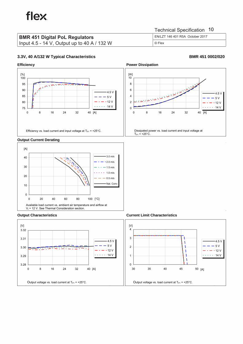
3.3V, 40 A/132 W Typical Characteristics BMR 451 0002/020
Efficiency Power Dissipation
75
80
85
90
95
100
0 8 16 24 32 40 [A]
[%]
4.5 V
5 V
12 V
14 V
0
2
4
6
8
10
0 8 16 24 32 40 [A]
[W]
4.5 V5 V12 V14 V
Efficiency vs. load current and input voltage at TP1 = +25°C. Dissipated power vs. load current and input voltage at TP1 = +25°C.
Output Current Derating
0
10
20
30
40
0 20 40 60 80 100 [°C]
[A]
3.0 m/s
2.0 m/s
1.5 m/s
1.0 m/s
0.5 m/s
Nat. Conv.
Available load current vs. ambient air temperature and airflow at VI = 12 V. See Thermal Consideration section.
Output Characteristics Current Limit Characteristics
3.28
3.29
3.30
3.31
3.32
0 8 16 24 32 40 [A]
[V]
4.5 V5 V12 V14 V
0
1
2
3
4
30 35 40 45 50 [A]
[V]
4.5 V5 V12 V14 V
Output voltage vs. load current at TP1 = +25°C. Output voltage vs. load current at TP1 = +25°C.
BMR 451 Digital PoL RegulatorsInput 4.5 - 14 V, Output up to 40 A / 132 W
EN/LZT 146 401 R5A October 2017
© Flex
Technical Specification 10
Ericsson Internal PRODUCT SPEC 8 (9)
Prepared (also subject responsible if other) No.
ETORHOL, EKAMAGN, EJANARV 2/1301-BMR 451 0002 Uen Approved Checked Date Rev Reference
SEC/D (Julia You) ETORHOL 2010-03-02 E
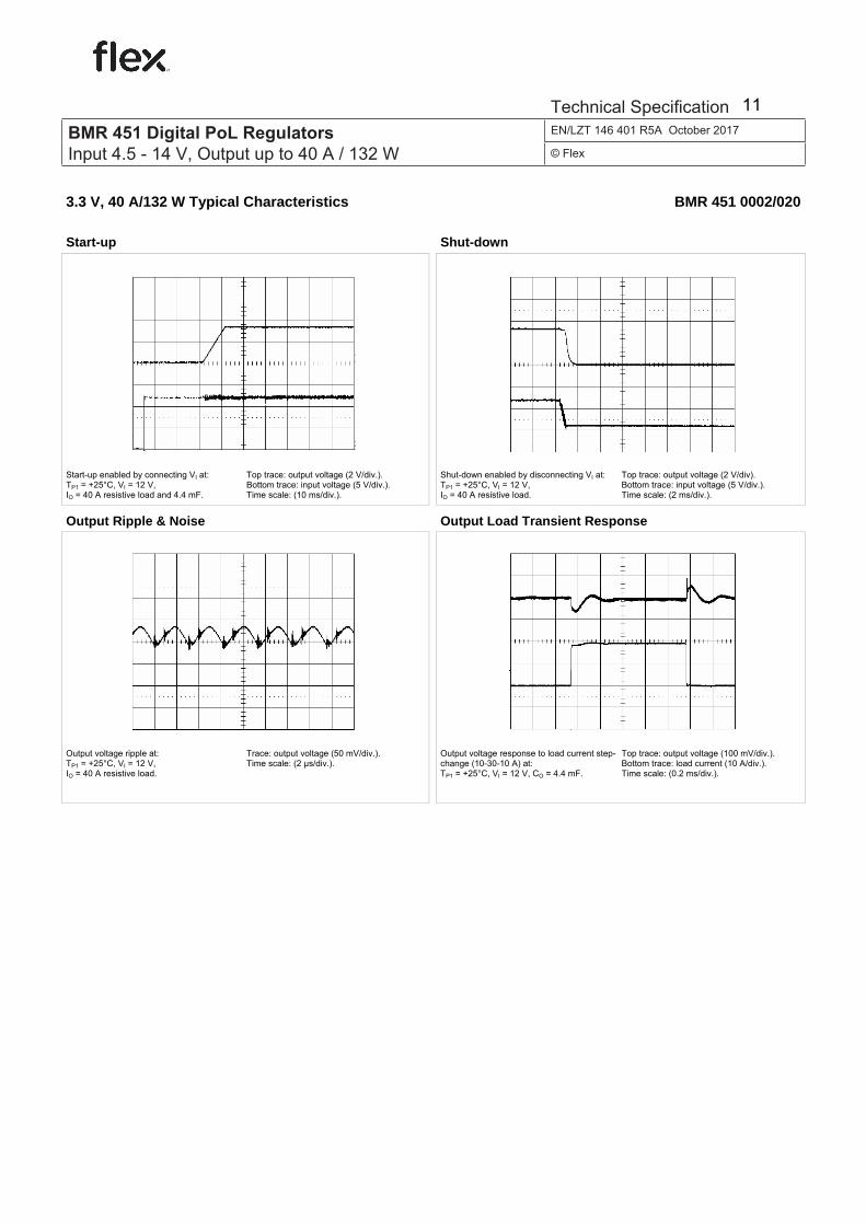
3.3 V, 40 A/132 W Typical Characteristics BMR 451 0002/020
Start-up Shut-down
Start-up enabled by connecting VI at: TP1 = +25°C, VI = 12 V, IO = 40 A resistive load and 4.4 mF.
Top trace: output voltage (2 V/div.). Bottom trace: input voltage (5 V/div.). Time scale: (10 ms/div.).
Shut-down enabled by disconnecting VI at: TP1 = +25°C, VI = 12 V, IO = 40 A resistive load.
Top trace: output voltage (2 V/div). Bottom trace: input voltage (5 V/div.). Time scale: (2 ms/div.).
Output Ripple & Noise Output Load Transient Response
Output voltage ripple at: TP1 = +25°C, VI = 12 V, IO = 40 A resistive load.
Trace: output voltage (50 mV/div.). Time scale: (2 µs/div.).
Output voltage response to load current step-change (10-30-10 A) at: TP1 = +25°C, VI = 12 V, CO = 4.4 mF.
Top trace: output voltage (100 mV/div.). Bottom trace: load current (10 A/div.). Time scale: (0.2 ms/div.).
BMR 451 Digital PoL RegulatorsInput 4.5 - 14 V, Output up to 40 A / 132 W
EN/LZT 146 401 R5A October 2017
© Flex
Technical Specification 11
PRODUCT SPECIFICATION
1 (7) Prepared (also subject responsible if other) No.
Rainbo 30/1301-BMR 451 0002 Uen Approved Checked Date Rev Reference
2017-10-19 J
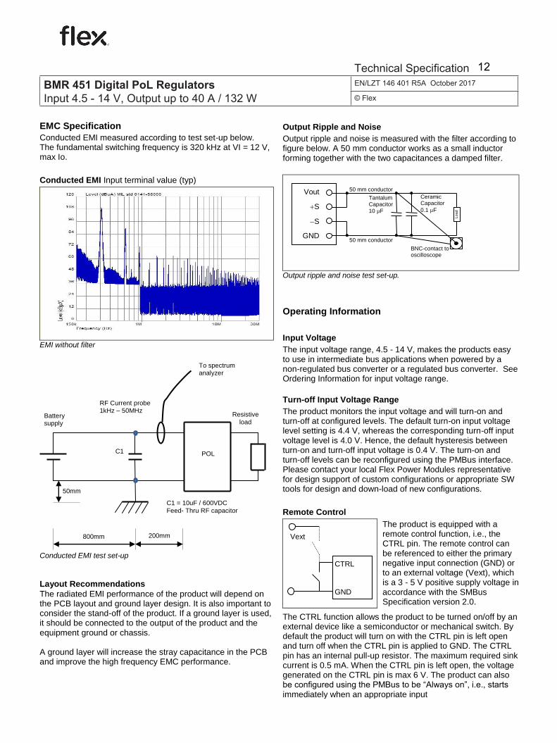
EMC Specification
Conducted EMI measured according to test set-up below. The fundamental switching frequency is 320 kHz at VI = 12 V, max Io.
Conducted EMI Input terminal value (typ)
EMI without filter
RF Current probe 1kHz – 50MHz
C1
To spectrum analyzer
POL
Resistive load
Battery supply
C1 = 10uF / 600VDC
Feed- Thru RF capacitor
800mm 200mm
50mm
Conducted EMI test set-up
Layout Recommendations The radiated EMI performance of the product will depend on the PCB layout and ground layer design. It is also important to consider the stand-off of the product. If a ground layer is used, it should be connected to the output of the product and the equipment ground or chassis. A ground layer will increase the stray capacitance in the PCB and improve the high frequency EMC performance.
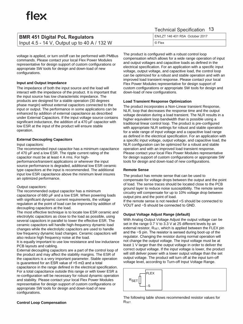
Output Ripple and Noise Output ripple and noise is measured with the filter according to figure below. A 50 mm conductor works as a small inductor forming together with the two capacitances a damped filter.
Output ripple and noise test set-up.
Operating Information
Input Voltage The input voltage range, 4.5 - 14 V, makes the products easy to use in intermediate bus applications when powered by a non-regulated bus converter or a regulated bus converter. See Ordering Information for input voltage range.
Turn-off Input Voltage Range The product monitors the input voltage and will turn-on and turn-off at configured levels. The default turn-on input voltage level setting is 4.4 V, whereas the corresponding turn-off input voltage level is 4.0 V. Hence, the default hysteresis between turn-on and turn-off input voltage is 0.4 V. The turn-on and turn-off levels can be reconfigured using the PMBus interface. Please contact your local Flex Power Modules representative for design support of custom configurations or appropriate SW tools for design and down-load of new configurations.
Remote Control
The product is equipped with a remote control function, i.e., the CTRL pin. The remote control can be referenced to either the primary negative input connection (GND) or to an external voltage (Vext), which is a 3 - 5 V positive supply voltage in accordance with the SMBus Specification version 2.0.
The CTRL function allows the product to be turned on/off by an external device like a semiconductor or mechanical switch. By default the product will turn on with the CTRL pin is left open and turn off when the CTRL pin is applied to GND. The CTRL pin has an internal pull-up resistor. The maximum required sink current is 0.5 mA. When the CTRL pin is left open, the voltage generated on the CTRL pin is max 6 V. The product can also be configured using the PMBus to be “Always on”, i.e., starts immediately when an appropriate input
Vout
S
S
GND
Ceramic Capacitor
0.1 µF
Tantalum Capacitor
10 µF
Lo
ad
50 mm conductor
50 mm conductor
BNC-contact to oscilloscope
CTRL
GND
Vext
BMR 451 Digital PoL RegulatorsInput 4.5 - 14 V, Output up to 40 A / 132 W
EN/LZT 146 401 R5A October 2017
© Flex
Technical Specification 12
PRODUCT SPECIFICATION
2 (7) Prepared (also subject responsible if other) No.
Rainbo 30/1301-BMR 451 0002 Uen Approved Checked Date Rev Reference
2017-10-19 J
voltage is applied, or turn on/off can be performed with PMBus commands. Please contact your local Flex Power Modules representative for design support of custom configurations or appropriate SW tools for design and down-load of new configurations.
Input and Output Impedance The impedance of both the input source and the load will interact with the impedance of the product. It is important that the input source has low characteristic impedance. The products are designed for a stable operation (30 degrees phase margin) without external capacitors connected to the input or output. The performance in some applications can be enhanced by addition of external capacitance as described under External Capacitors. If the input voltage source contains significant inductance, the addition of a 470 µF capacitor with low ESR at the input of the product will ensure stable operation.
External Decoupling Capacitors Input capacitors: The recommended input capacitor has a minimum capacitance of 470 µF and a low ESR. The ripple current rating of the capacitor must be at least 4 A rms. For high-performance/transient applications or wherever the input source performance is degraded, additional low ESR ceramic type capacitors at the input is recommended. The additional input low ESR capacitance above the minimum level insures an optimized performance. Output capacitors: The recommended output capacitor has a minimum capacitance of 680 µF and a low ESR. When powering loads with significant dynamic current requirements, the voltage regulation at the point of load can be improved by addition of decoupling capacitors at the load. The most effective technique is to locate low ESR ceramic and electrolytic capacitors as close to the load as possible, using several capacitors in parallel to lower the effective ESR. The ceramic capacitors will handle high-frequency dynamic load changes while the electrolytic capacitors are used to handle low frequency dynamic load changes. Ceramic capacitors will also reduce high frequency noise at the load. It is equally important to use low resistance and low inductance PCB layouts and cabling. External decoupling capacitors are a part of the control loop of the product and may affect the stability margins. The ESR of the capacitors is a very important parameter. Stable operation is guaranteed for an ESR value of >5 mΩ and a total capacitance in the range defined in the electrical specification. For a total capacitance outside this range or with lower ESR a re-configuration will be necessary for robust dynamic operation and stability. Please contact your local Flex Power Modules representative for design support of custom configurations or appropriate SW tools for design and down-load of new configurations.
Control Loop Compensation
The product is configured with a robust control loop compensation which allows for a wide range operation of input and output voltages and capacitive loads as defined in the electrical specification. For an application with a specific input voltage, output voltage, and capacitive load, the control loop can be optimized for a robust and stable operation and with an improved load transient response. Please contact your local Flex Power Modules representative for design support of custom configurations or appropriate SW tools for design and down-load of new configurations.
Load Transient Response Optimization
The product incorporates a Non-Linear transient Response, NLR, loop that decreases the response time and the output voltage deviation during a load transient. The NLR results in a higher equivalent loop bandwidth than is possible using a traditional linear control loop. The product is pre-configured with appropriate NLR settings for robust and stable operation for a wide range of input voltage and a capacitive load range as defined in the electrical specification. For an application with a specific input voltage, output voltage, and capacitive load, the NLR configuration can be optimized for a robust and stable operation and with an improved load transient response. Please contact your local Flex Power Modules representative for design support of custom configurations or appropriate SW tools for design and down-load of new configurations. Remote Sense
The product has remote sense that can be used to compensate for voltage drops between the output and the point of load. The sense traces should be located close to the PCB ground layer to reduce noise susceptibility. The remote sense circuitry will compensate for up to 10% voltage drop between output pins and the point of load. If the remote sense is not needed +S should be connected to VOUT and −S should be connected to GND.
Output Voltage Adjust Range (default) With Analog Output Voltage Adjust the output voltage can be set in the range 0.7 V to 3.3 V at 25 different levels by an external resistor, RSET, which is applied between the FLEX pin and the −S pin. The resistor is sensed during boot-up of the regulator. Changing the resistor during normal operation will not change the output voltage. The input voltage must be at least 1 V larger than the output voltage in order to deliver the correct output voltage. If the input voltage is lower, the product will still deliver power with a lower output voltage than the set output voltage. The product will turn off at the input turn-off voltage level, according to Turn-off Input Voltage Range.
The following table shows recommended resistor values for RSET.
FLEX
S
RSET
BMR 451 Digital PoL RegulatorsInput 4.5 - 14 V, Output up to 40 A / 132 W
EN/LZT 146 401 R5A October 2017
© Flex
Technical Specification 13
PRODUCT SPECIFICATION
3 (7) Prepared (also subject responsible if other) No.
Rainbo 30/1301-BMR 451 0002 Uen Approved Checked Date Rev Reference
2017-10-19 J
VOUT [V]
Rset[kΩ]
VOUT [V]
Rset[kΩ]
Min Typ Max Min Typ Max
0.7 155.00 159.00 169.00 0.991 21.38 21.60 21.82
0.752 109.89 111.00 112.11 1.00 18.51 18.70 18.89
0.758 99.00 100.00 101.00 1.10 15.94 16.10 16.26
0.765 89.10 90.00 90.90 1.158 13.56 13.70 13.84
0.772 80.09 80.90 81.71 1.20 11.39 11.50 11.62
0.79 64.35 72.50 73.23 1.25 9.50 9.60 9.70
0.80 57.52 58.10 58.68 1.50 7.72 7.80 7.88
0.821 51.38 51.90 52.42 1.669 6.14 6.20 6.26
0.848 40.69 41.10 41.51 1.80 4.65 4.70 4.75
0.88 36.04 36.40 36.76 2.295 3.27 3.30 3.33
0.899 31.88 32.20 32.52 2.506 2.08 2.10 2.12
0.919 28.02 28.30 28.58 3.30 0.99 1.00 1.01
0.965 24.55 24.80 25.05
Output Voltage Adjust using PMBus The output voltage of the product can be reconfigured using the PMBus interface in the range 0.6 V to 3.6 V with the resolution of 1 mV. Please contact your local Flex Power Modules representative for design support of custom configurations or appropriate SW tools for design and down-load of new configurations. Maximum Output Voltage Protection
The regulator can be configured for maximum output voltage protection. The Analog Voltage Adjust sets the maximum output voltage equal to 10% higher than the nominal output value set by the RSET. This works as a hardware protection for the load, avoiding destroying the load by an over voltage. Please contact your local Flex Power Modules representative for design support of custom configurations or appropriate SW tools for design and down-load of new configurations.
Synchronization Synchronization is a feature that allows multiple DC/DC regulators to be synchronized to a common frequency. Synchronized regulators powered from the same bus eliminate beat frequencies reflected back to the input supply, and also reduces EMI filtering requirements. Eliminating the slow beat frequencies (usually < 10 kHz) allows the EMI filter to be designed to attenuate only the synchronization frequency. Synchronization can also be utilized for interleaving, described in section Interleaving. The product FLEX pin can be configured for synchronization. Hence, Analog Voltage Adjust is disabled, when the synchronization is enabled. The regulators can be synchronized with an external oscillator or one regulator can be configured with the FLEX pin as an SYNC Output working as a master driving the synchronization. All others on the same synchronization bus should be configured with SYNC Input or SYNC Auto Detect (Default configuration) for correct operation. When the FLEX pin is configured in auto
detect mode the product will automatically check for a clock signal on the FLEX pin. The switching frequency can also be set to any value between 200 kHz and 400 kHz using the PMBus interface. Please contact your local Flex Power Modules representative for design support of custom configurations or appropriate SW tools for design and down-load of new configurations.
Interleaving When multiple DC/DC regulators share a common DC input supply, interleaving, or spreading of the switching clock phase between the regulators can be utilized. This dramatically reduces input capacitance requirements and efficiency losses, since the peak current drawn from the input supply is effectively spread out over the whole switch period. This requires that the DC/DC regulators are synchronized. Up to 16 different interleaving phases can be used. The interleaving of the product can be reconfigured using the PMBus interface. Please contact your local Flex Power Modules representative for design support of custom configurations or appropriate SW tools for design and down-load of new configurations. Parallel Operation Parallel operation is not recommended. Over Temperature Protection (OTP)
The products are protected from thermal overload by an internal over temperature shutdown circuit. When TP1 as defined in thermal consideration section exceeds 120°C the product will shut down. The product will make continuous attempts to start up (non-latching mode) and resume normal operation automatically when the temperature has dropped >15°C below the temperature threshold. Please contact your local Flex Power Modules representative for design support of custom configurations or appropriate SW tools for design and down-load of new configurations.
Over Current Protection (OCP) The product includes current limiting circuitry for protection at continuous overload. The product will shut down immediately for output currents in excess of the current limit, Ilim. The product will try to restart every 70 ms, i.e., hiccup mode, and resume normal operation after removal of the overload. The load distribution should be designed for the maximum output short circuit current specified Please contact your local Flex Power Modules representative for design support of custom configurations or appropriate SW tools for design and down-load of new configurations. Soft-start Power Up The soft-start control introduces a time-delay (default setting 10 ms) before allowing the output voltage to rise. The default rise time of the ramp up is 10 ms. Power-up is hence completed within 20 ms in default configuration using remote control. When starting by applying input voltage the control circuit boot-up time adds an additional 10 ms delay. Please contact your local Flex Power Modules representative for design support of custom configurations or appropriate SW tools for design and
BMR 451 Digital PoL RegulatorsInput 4.5 - 14 V, Output up to 40 A / 132 W
EN/LZT 146 401 R5A October 2017
© Flex
Technical Specification 14
PRODUCT SPECIFICATION
4 (7) Prepared (also subject responsible if other) No.
Rainbo 30/1301-BMR 451 0002 Uen Approved Checked Date Rev Reference
2017-10-19 J
down-load of new configurations. Output Voltage Sequencing
A group of regulators may be configured to power up in a predetermined sequence. This feature is especially useful when powering advanced processors, FPGAs, and ASICs that require one supply to reach its operating voltage prior to another supply reaching its operating voltage. Multi-regulator sequencing can be achieved by configuring each device start delay and rise time through the PMBus and use the same remote control start signal. Please contact your local Flex Power Modules representative for design support of custom configurations or appropriate SW tools for design and down-load of new configurations.
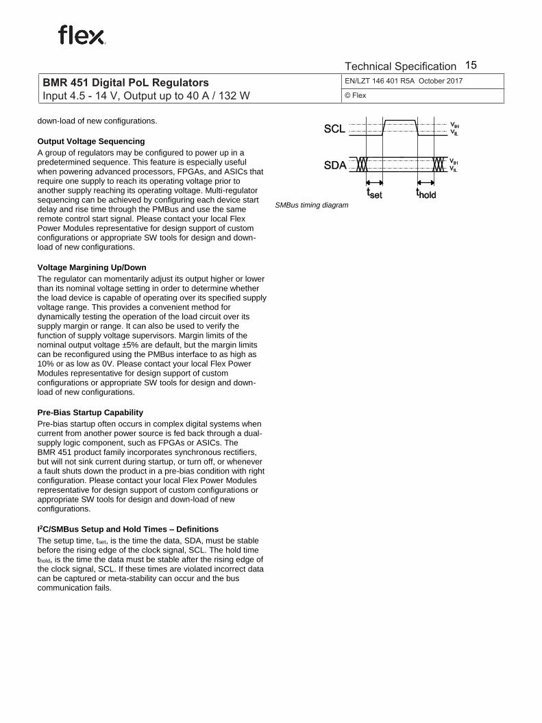
Voltage Margining Up/Down The regulator can momentarily adjust its output higher or lower than its nominal voltage setting in order to determine whether the load device is capable of operating over its specified supply voltage range. This provides a convenient method for dynamically testing the operation of the load circuit over its supply margin or range. It can also be used to verify the function of supply voltage supervisors. Margin limits of the nominal output voltage ±5% are default, but the margin limits can be reconfigured using the PMBus interface to as high as 10% or as low as 0V. Please contact your local Flex Power Modules representative for design support of custom configurations or appropriate SW tools for design and down-load of new configurations. Pre-Bias Startup Capability Pre-bias startup often occurs in complex digital systems when current from another power source is fed back through a dual-supply logic component, such as FPGAs or ASICs. The BMR 451 product family incorporates synchronous rectifiers, but will not sink current during startup, or turn off, or whenever a fault shuts down the product in a pre-bias condition with right configuration. Please contact your local Flex Power Modules representative for design support of custom configurations or appropriate SW tools for design and down-load of new configurations. I2C/SMBus Setup and Hold Times – Definitions The setup time, tset, is the time the data, SDA, must be stable before the rising edge of the clock signal, SCL. The hold time thold, is the time the data must be stable after the rising edge of the clock signal, SCL. If these times are violated incorrect data can be captured or meta-stability can occur and the bus communication fails.
SMBus timing diagram
BMR 451 Digital PoL RegulatorsInput 4.5 - 14 V, Output up to 40 A / 132 W
EN/LZT 146 401 R5A October 2017
© Flex
Technical Specification 15
PRODUCT SPECIFICATION
5 (7) Prepared (also subject responsible if other) No.
Rainbo 30/1301-BMR 451 0002 Uen Approved Checked Date Rev Reference
2017-10-19 J
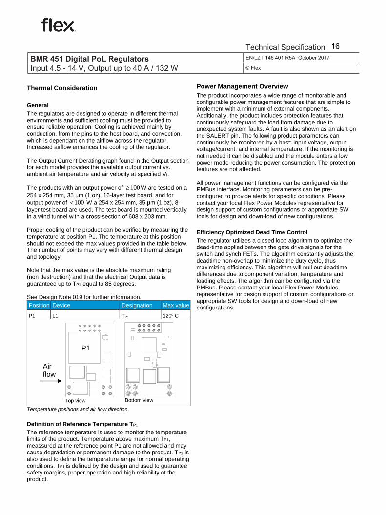
Thermal Consideration General The regulators are designed to operate in different thermal environments and sufficient cooling must be provided to ensure reliable operation. Cooling is achieved mainly by conduction, from the pins to the host board, and convection, which is dependant on the airflow across the regulator. Increased airflow enhances the cooling of the regulator. The Output Current Derating graph found in the Output section for each model provides the available output current vs. ambient air temperature and air velocity at specified VI.
The products with an output power of 100 W are tested on a
254 x 254 mm, 35 µm (1 oz), 16-layer test board, and for
output power of 100 W a 254 x 254 mm, 35 µm (1 oz), 8-
layer test board are used. The test board is mounted vertically in a wind tunnel with a cross-section of 608 x 203 mm. Proper cooling of the product can be verified by measuring the temperature at position P1. The temperature at this position should not exceed the max values provided in the table below. The number of points may vary with different thermal design and topology. Note that the max value is the absolute maximum rating (non destruction) and that the electrical Output data is guaranteed up to TP1 equal to 85 degrees. See Design Note 019 for further information.
Position Device Designation Max value
P1 L1 TP1 120º C
Temperature positions and air flow direction.
Definition of Reference Temperature TP1 The reference temperature is used to monitor the temperature limits of the product. Temperature above maximum TP1, meassured at the reference point P1 are not allowed and may cause degradation or permanent damage to the product. TP1 is also used to define the temperature range for normal operating conditions. TP1 is defined by the design and used to guarantee safety margins, proper operation and high reliability ot the product.
Power Management Overview
The product incorporates a wide range of monitorable and configurable power management features that are simple to implement with a minimum of external components. Additionally, the product includes protection features that continuously safeguard the load from damage due to unexpected system faults. A fault is also shown as an alert on the SALERT pin. The following product parameters can continuously be monitored by a host: Input voltage, output voltage/current, and internal temperature. If the monitoring is not needed it can be disabled and the module enters a low power mode reducing the power consumption. The protection features are not affected. All power management functions can be configured via the PMBus interface. Monitoring parameters can be pre-configured to provide alerts for specific conditions. Please contact your local Flex Power Modules representative for design support of custom configurations or appropriate SW tools for design and down-load of new configurations.
Efficiency Optimized Dead Time Control The regulator utilizes a closed loop algorithm to optimize the dead-time applied between the gate drive signals for the switch and synch FETs. The algorithm constantly adjusts the deadtime non-overlap to minimize the duty cycle, thus maximizing efficiency. This algorithm will null out deadtime differences due to component variation, temperature and loading effects. The algorithm can be configured via the PMBus. Please contact your local Flex Power Modules representative for design support of custom configurations or appropriate SW tools for design and down-load of new configurations.
P1
Air flow
Bottom view Top view
BMR 451 Digital PoL RegulatorsInput 4.5 - 14 V, Output up to 40 A / 132 W
EN/LZT 146 401 R5A October 2017
© Flex
Technical Specification 16
PRODUCT SPECIFICATION
6 (7) Prepared (also subject responsible if other) No.
Rainbo 30/1301-BMR 451 0002 Uen Approved Checked Date Rev Reference
2017-10-19 J
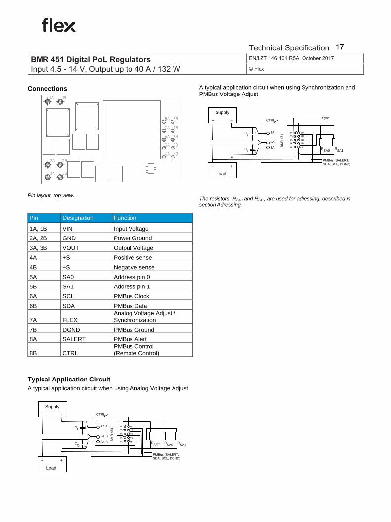
Connections
Pin layout, top view.
Pin Designation Function
1A, 1B VIN Input Voltage
2A, 2B GND Power Ground
3A, 3B VOUT Output Voltage
4A +S Positive sense
4B −S Negative sense
5A SA0 Address pin 0
5B SA1 Address pin 1
6A SCL PMBus Clock
6B SDA PMBus Data
7A FLEX Analog Voltage Adjust / Synchronization
7B DGND PMBus Ground
8A SALERT PMBus Alert
8B CTRL PMBus Control (Remote Control)
Typical Application Circuit A typical application circuit when using Analog Voltage Adjust.
A typical application circuit when using Synchronization and PMBus Voltage Adjust.
The resistors, RSA0 and RSA1, are used for adressing, described in section Adressing.
1A,B
2A,B
3A,B
8A 8B
7A 7B
6A 6B
5A 5B
4A 4B
Load
CO
Supply
CI
RSET
CTRL
PMBus (SALERT, SDA, SCL, DGND)
RSA0
RSA1
BM
R 4
51
1A
2A
3A
Load
CO
Supply
CI
CTRL
PMBus (SALERT, SDA, SCL, DGND)
RSA0
RSA1
BM
R 4
51
Sync
8A 8B
7A 7B
6A 6B
5A 5B
4A 4B
BMR 451 Digital PoL RegulatorsInput 4.5 - 14 V, Output up to 40 A / 132 W
EN/LZT 146 401 R5A October 2017
© Flex
Technical Specification 17
PMBus Interface
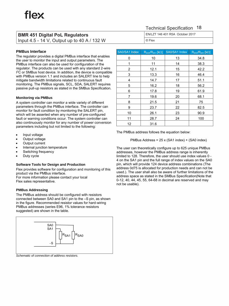
The regulator provides a digital PMBus interface that enables the user to monitor the input and output parameters. The PMBus interface can also be used for configuration of the regulator. The products can be used with any standard 2-wire I2C or SMBus host device. In addition, the device is compatible with PMBus version 1.1 and includes an SALERT line to help mitigate bandwidth limitations related to continuous fault monitoring. The PMBus signals, SCL, SDA, SALERT requires passive pull-up resistors as stated in the SMBus Specification. Monitoring via PMBus
A system controller can monitor a wide variety of different parameters through the PMBus interface. The controller can monitor for fault condition by monitoring the SALERT pin, which will be asserted when any number of pre-configured fault or warning conditions occur. The system controller can also continuously monitor for any number of power conversion parameters including but not limited to the following: • Input voltage • Output voltage • Output current • Internal junction temperature • Switching frequency • Duty cycle Software Tools for Design and Production Flex provides software for configuration and monitoring of this product via the PMBus interface. For more information please contact your local Flex sales representative. PMBus Addressing The PMBus address should be configured with resistors connected between SA0 and SA1 pin to the –S pin, as shown in the figure. Recommended resistor values for hard-wiring PMBus addresses (series E96, 1% tolerance resistors suggested) are shown in the table.
Schematic of connection of address resistors.
SA0/SA1 Index RSA0/RSA1 [k] SA0/SA1 Index RSA0/RSA1 [k] 1 2 3 4 5 6 7 8 9 10 11 12 13 14 15 16 17 18
0 10 13 34.8 1 11 14 38.3 2 12.1 15 42.2 3 13.3 16 46.4 4 14.7 17 51.1 5 16.2 18 56.2 6 17.8 19 61.9 7 19.6 20 68.1 8 21.5 21 75 9 23.7 22 82.5
10 26.1 23 90.9 11 28.7 24 100 12 31.6
The PMBus address follows the equation below:
PMBus Address = 25 x (SA1 index) + (SA0 index) The user can theoretically configure up to 625 unique PMBus addresses, however the PMBus address range is inherently limited to 128. Therefore, the user should use index values 0 - 4 on the SA1 pin and the full range of index values on the SA0 pin, which will provide 124 device address combinations (The address 0d75 is allocated for production needs and can not be used.). The user shall also be aware of further limitations of the address space as stated in the SMBus Specification(Note that 0-12, 40, 44, 45, 55, 64-68 in decimal are reserved and may not be usable).
SA0 SA1
S
RSA1 RSA0
BMR 451 Digital PoL RegulatorsInput 4.5 - 14 V, Output up to 40 A / 132 W
EN/LZT 146 401 R5A October 2017
© Flex
Technical Specification 18
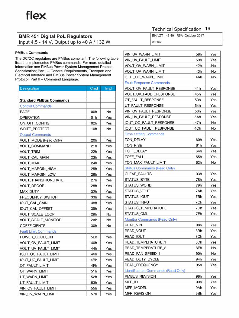
PMBus Commands The DC/DC regulators are PMBus compliant. The following table lists the implemented PMBus commands. For more detailed information see PMBus Power System Management Protocol Specification; Part I – General Requirements, Transport and Electrical Interface and PMBus Power System Management Protocol; Part II – Command Language.
Designation Cmd Impl
Standard PMBus Commands Control Commands
PAGE 00h No
OPERATION 01h Yes
ON_OFF_CONFIG 02h Yes
WRITE_PROTECT 10h No
Output Commands
VOUT_MODE (Read Only) 20h Yes
VOUT_COMMAND 21h Yes
VOUT_TRIM 22h Yes
VOUT_CAL_GAIN 23h Yes
VOUT_MAX 24h Yes
VOUT_MARGIN_HIGH 25h Yes
VOUT_MARGIN_LOW 26h Yes
VOUT_TRANSITION_RATE 27h Yes
VOUT_DROOP 28h Yes
MAX_DUTY 32h Yes
FREQUENCY_SWITCH 33h Yes
IOUT_CAL_GAIN 38h Yes
IOUT_CAL_OFFSET 39h Yes
VOUT_SCALE_LOOP 29h No
VOUT_SCALE_MONITOR 2Ah No
COEFFICIENTS 30h No
Fault Limit Commands
POWER_GOOD_ON 5Eh Yes
VOUT_OV_FAULT_LIMIT 40h Yes
VOUT_UV_FAULT_LIMIT 44h Yes
IOUT_OC_FAULT_LIMIT 46h Yes
IOUT_UC_FAULT_LIMIT 4Bh Yes
OT_FAULT_LIMIT 4Fh Yes
OT_WARN_LIMIT 51h Yes
UT_WARN_LIMIT 52h Yes
UT_FAULT_LIMIT 53h Yes
VIN_OV_FAULT_LIMIT 55h Yes
VIN_OV_WARN_LIMIT 57h Yes
VIN_UV_WARN_LIMIT 58h Yes
VIN_UV_FAULT_LIMIT 59h Yes
VOUT_OV_WARN_LIMIT 42h No
VOUT_UV_WARN_LIMIT 43h No
IOUT_OC_WARN_LIMIT 4Ah No
Fault Response Commands
VOUT_OV_FAULT_RESPONSE 41h Yes VOUT_UV_FAULT_RESPONSE 45h Yes OT_FAULT_RESPONSE 50h Yes UT_FAULT_RESPONSE 54h Yes VIN_OV_FAULT_RESPONSE 56h Yes VIN_UV_FAULT_RESPONSE 5Ah Yes IOUT_OC_FAULT_RESPONSE 47h No IOUT_UC_FAULT_RESPONSE 4Ch No Time setting Commands
TON_DELAY 60h Yes TON_RISE 61h Yes TOFF_DELAY 64h Yes TOFF_FALL 65h Yes
TON_MAX_FAULT_LIMIT 62h No
Status Commands (Read Only)
CLEAR_FAULTS 03h Yes STATUS_BYTE 78h Yes STATUS_WORD 79h Yes STATUS_VOUT 7Ah Yes STATUS_IOUT 7Bh Yes STATUS_INPUT 7Ch Yes STATUS_TEMPERATURE 7Dh Yes STATUS_CML 7Eh Yes
Monitor Commands (Read Only)
READ_VIN 88h Yes READ_VOUT 8Bh Yes READ_IOUT 8Ch Yes READ_TEMPERATURE_1 8Dh Yes READ_TEMPERATURE_2 8Eh No READ_FAN_SPEED_1 90h No READ_DUTY_CYCLE 94h Yes READ_FREQUENCY 95h Yes
Identification Commands (Read Only)
PMBUS_REVISION 98h Yes MFR_ID 99h Yes MFR_MODEL 9Ah Yes MFR_REVISION 9Bh Yes
BMR 451 Digital PoL RegulatorsInput 4.5 - 14 V, Output up to 40 A / 132 W
EN/LZT 146 401 R5A October 2017
© Flex
Technical Specification 19
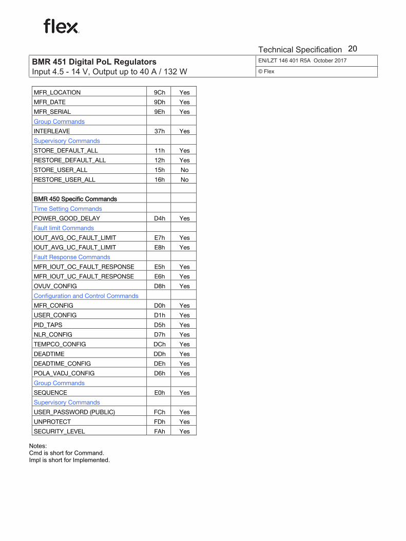
MFR_LOCATION 9Ch Yes MFR_DATE 9Dh Yes MFR_SERIAL 9Eh Yes
Group Commands
INTERLEAVE 37h Yes
Supervisory Commands
STORE_DEFAULT_ALL 11h Yes
RESTORE_DEFAULT_ALL 12h Yes
STORE_USER_ALL 15h No
RESTORE_USER_ALL 16h No
BMR 450 Specific Commands
Time Setting Commands
POWER_GOOD_DELAY D4h Yes
Fault limit Commands
IOUT_AVG_OC_FAULT_LIMIT E7h Yes
IOUT_AVG_UC_FAULT_LIMIT E8h Yes
Fault Response Commands
MFR_IOUT_OC_FAULT_RESPONSE E5h Yes
MFR_IOUT_UC_FAULT_RESPONSE E6h Yes
OVUV_CONFIG D8h Yes
Configuration and Control Commands
MFR_CONFIG D0h Yes
USER_CONFIG D1h Yes
PID_TAPS D5h Yes
NLR_CONFIG D7h Yes
TEMPCO_CONFIG DCh Yes
DEADTIME DDh Yes
DEADTIME_CONFIG DEh Yes
POLA_VADJ_CONFIG D6h Yes
Group Commands
SEQUENCE E0h Yes
Supervisory Commands
USER_PASSWORD (PUBLIC) FCh Yes
UNPROTECT FDh Yes
SECURITY_LEVEL FAh Yes
Notes: Cmd is short for Command. Impl is short for Implemented.
BMR 451 Digital PoL RegulatorsInput 4.5 - 14 V, Output up to 40 A / 132 W
EN/LZT 146 401 R5A October 2017
© Flex
Technical Specification 20
Ericsson Internal PRODUCT SPEC. MECHANICAL 1 (3)
Prepared (also subject responsible if other) No.
EPETSCH 4/1301 BMR 451 Uen Approved Checked Date Rev Reference
EAB/FJB/GMF [Natalie J] See §1 2009-03-24 B
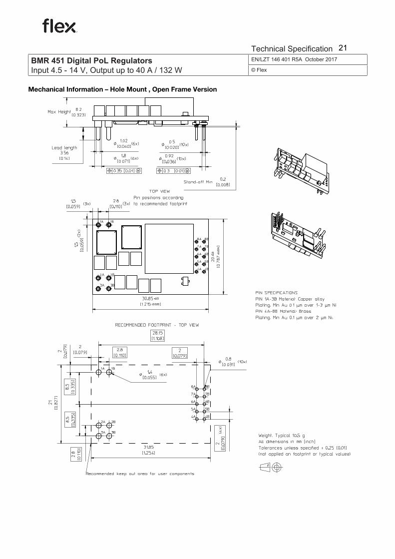
Mechanical Information — Hole Mount , Open Frame Version
BMR 451 Digital PoL RegulatorsInput 4.5 - 14 V, Output up to 40 A / 132 W
EN/LZT 146 401 R5A October 2017
© Flex
Technical Specification 21
Ericsson Internal PRODUCT SPEC. MECHANICAL 2 (3)
Prepared (also subject responsible if other) No.
EPETSCH 4/1301 BMR 451 Uen Approved Checked Date Rev Reference
EAB/FJB/GMF [Natalie J] See §1 2009-03-24 B
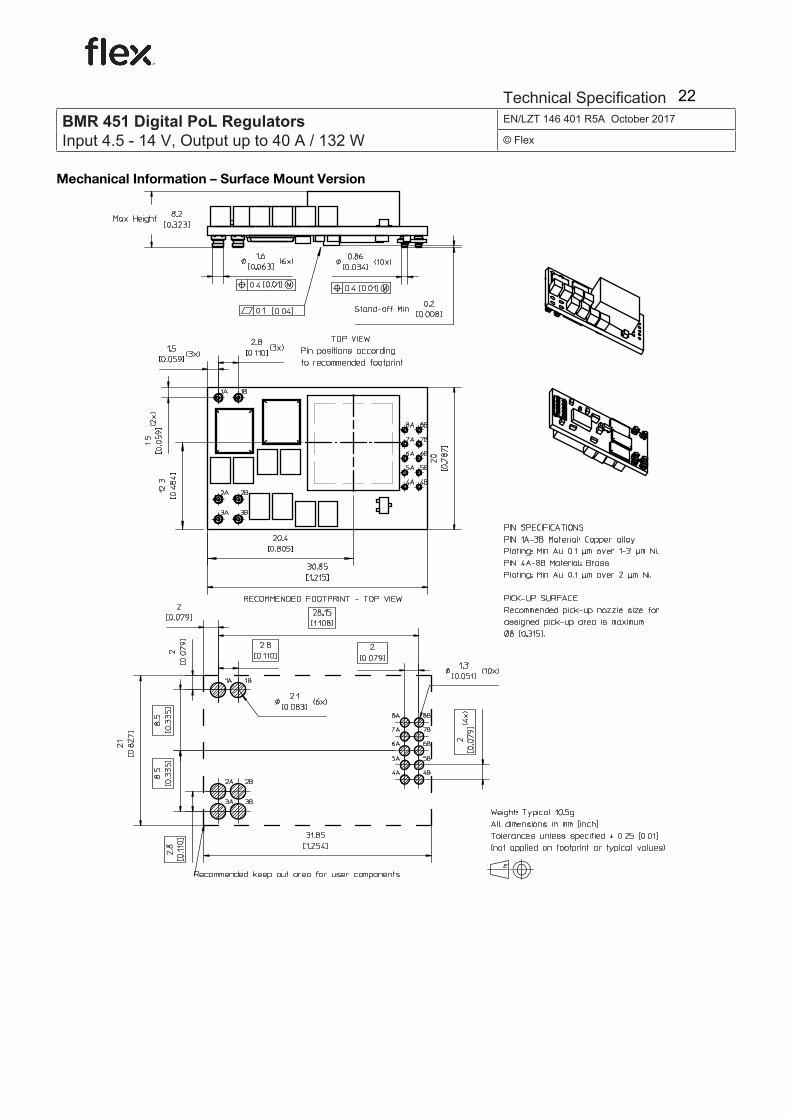
Mechanical Information — Surface Mount Version
BMR 451 Digital PoL RegulatorsInput 4.5 - 14 V, Output up to 40 A / 132 W
EN/LZT 146 401 R5A October 2017
© Flex
Technical Specification 22
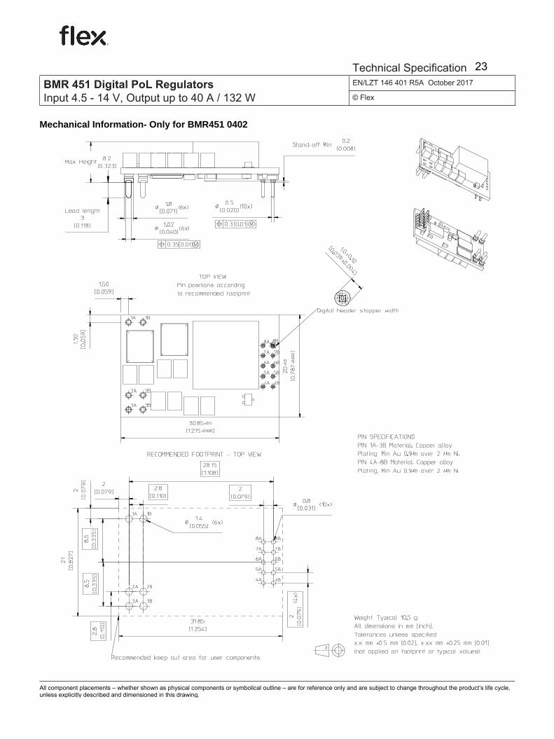
Mechanical Information- Only for BMR451 0402
All component placements – whether shown as physical components or symbolical outline – are for reference only and are subject to change throughout the product’s life cycle, unless explicitly described and dimensioned in this drawing.
BMR 451 Digital PoL RegulatorsInput 4.5 - 14 V, Output up to 40 A / 132 W
EN/LZT 146 401 R5A October 2017
© Flex
Technical Specification 23
Ericsson Internal PRODUCT SPEC. 1 (4)
Prepared (also subject responsible if other) No.
EPETSCH 5/1301- BMR 451 Uen Approved Checked Date Rev Reference
SEC/D (Julia You) See §1 2010-03-10 B
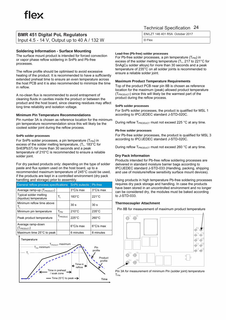
Soldering Information - Surface MountingThe surface mount product is intended for forced convection or vapor phase reflow soldering in SnPb and Pb-free processes. The reflow profile should be optimised to avoid excessive heating of the product. It is recommended to have a sufficiently extended preheat time to ensure an even temperature across the host PCB and it is also recommended to minimize the time in reflow. A no-clean flux is recommended to avoid entrapment of cleaning fluids in cavities inside the product or between the product and the host board, since cleaning residues may affect long time reliability and isolation voltage. Minimum Pin Temperature Recommendations Pin number 3A is chosen as reference location for the minimum pin temperature recommendation since this will likely be the coolest solder joint during the reflow process. SnPb solder processes
For SnPb solder processes, a pin temperature (TPIN) in excess of the solder melting temperature, (TL, 183°C for Sn63Pb37) for more than 30 seconds and a peak temperature of 210°C is recommended to ensure a reliable solder joint. For dry packed products only: depending on the type of solder paste and flux system used on the host board, up to a recommended maximum temperature of 245°C could be used, if the products are kept in a controlled environment (dry pack handling and storage) prior to assembly. General reflow process specifications SnPb eutectic Pb-free
Average ramp-up (TPRODUCT) 3°C/s max 3°C/s max Typical solder melting (liquidus) temperature TL 183°C 221°C
Minimum reflow time above TL
30 s 30 s
Minimum pin temperature TPIN 210°C 235°C
Peak product temperature TPRODUC
T 225°C 260°C
Average ramp-down (TPRODUCT) 6°C/s max 6°C/s max
Maximum time 25°C to peak 6 minutes 8 minutes
TPRODUCT maximum TPIN minimum
Time
Pin profile
Productprofile
TL
Time in reflow
Time in preheat / soak zone
Time 25°C to peak
Temperature
Lead-free (Pb-free) solder processes For Pb-free solder processes, a pin temperature (TPIN) in excess of the solder melting temperature (TL, 217 to 221°C for SnAgCu solder alloys) for more than 30 seconds and a peak temperature of 235°C on all solder joints is recommended to ensure a reliable solder joint. Maximum Product Temperature Requirements Top of the product PCB near pin 8B is chosen as reference location for the maximum (peak) allowed product temperature (TPRODUCT) since this will likely be the warmest part of the product during the reflow process. SnPb solder processes
For SnPb solder processes, the product is qualified for MSL 1 according to IPC/JEDEC standard J-STD-020C. During reflow TPRODUCT must not exceed 225 °C at any time. Pb-free solder processes
For Pb-free solder processes, the product is qualified for MSL 3 according to IPC/JEDEC standard J-STD-020C. During reflow TPRODUCT must not exceed 260 °C at any time.
Dry Pack Information Products intended for Pb-free reflow soldering processes are delivered in standard moisture barrier bags according to IPC/JEDEC standard J-STD-033 (Handling, packing, shipping and use of moisture/reflow sensitivity surface mount devices). Using products in high temperature Pb-free soldering processes requires dry pack storage and handling. In case the products have been stored in an uncontrolled environment and no longer can be considered dry, the modules must be baked according to J-STD-033. Thermocoupler Attachment
Pin 3A for measurement of minimum Pin (solder joint) temperature TPIN
Pin 8B for measurement of maximum product temperature
BMR 451 Digital PoL RegulatorsInput 4.5 - 14 V, Output up to 40 A / 132 W
EN/LZT 146 401 R5A October 2017
© Flex
Technical Specification 24
Ericsson Internal PRODUCT SPEC. 2 (4)
Prepared (also subject responsible if other) No.
EPETSCH 5/1301- BMR 451 Uen Approved Checked Date Rev Reference
SEC/D (Julia You) See §1 2010-03-10 B
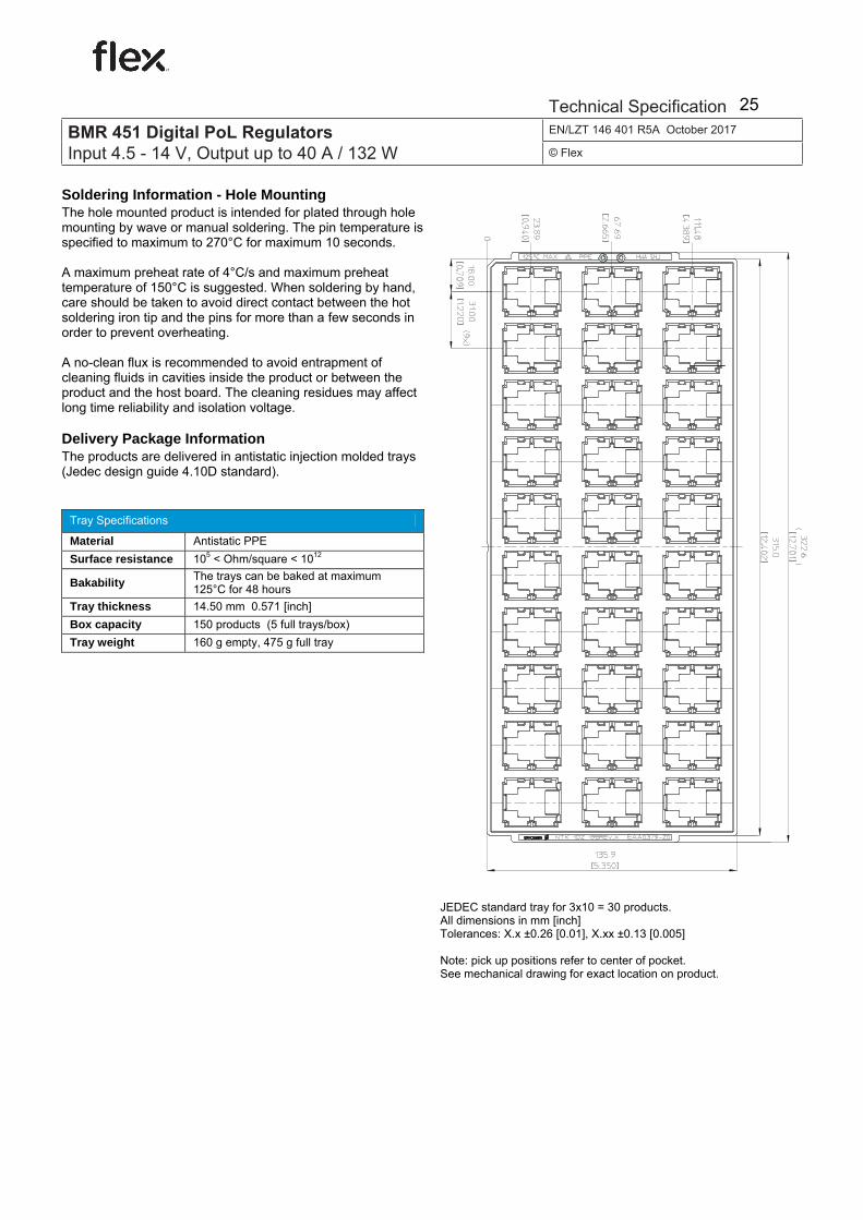
Soldering Information - Hole Mounting The hole mounted product is intended for plated through hole mounting by wave or manual soldering. The pin temperature is specified to maximum to 270°C for maximum 10 seconds. A maximum preheat rate of 4°C/s and maximum preheat temperature of 150°C is suggested. When soldering by hand, care should be taken to avoid direct contact between the hot soldering iron tip and the pins for more than a few seconds in order to prevent overheating. A no-clean flux is recommended to avoid entrapment of cleaning fluids in cavities inside the product or between the product and the host board. The cleaning residues may affect long time reliability and isolation voltage. Delivery Package Information The products are delivered in antistatic injection molded trays (Jedec design guide 4.10D standard).
Tray Specifications
Material Antistatic PPE Surface resistance 105 < Ohm/square < 1012
Bakability The trays can be baked at maximum 125°C for 48 hours
Tray thickness 14.50 mm 0.571 [inch] Box capacity 150 products (5 full trays/box) Tray weight 160 g empty, 475 g full tray
JEDEC standard tray for 3x10 = 30 products. All dimensions in mm [inch] Tolerances: X.x ±0.26 [0.01], X.xx ±0.13 [0.005] Note: pick up positions refer to center of pocket. See mechanical drawing for exact location on product.
BMR 451 Digital PoL RegulatorsInput 4.5 - 14 V, Output up to 40 A / 132 W
EN/LZT 146 401 R5A October 2017
© Flex
Technical Specification 25
Ericsson Internal PRODUCT SPEC. 1 (4)
Prepared (also subject responsible if other) No.
EPEIHLI 5/1301- BMR 451 0402 Uen Approved Checked Date Rev Reference
SEC/D (Lisa Li) See §1 2015-05-18 A
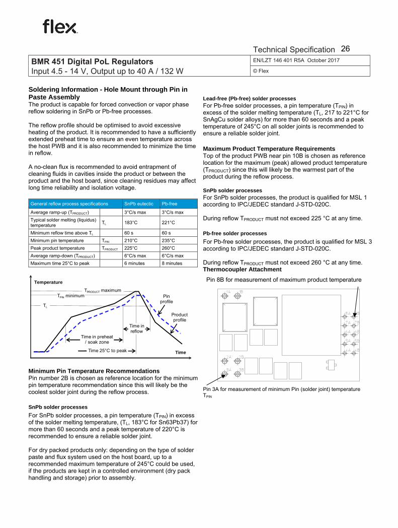
Soldering Information - Hole Mount through Pin in Paste Assembly The product is capable for forced convection or vapor phase reflow soldering in SnPb or Pb-free processes. The reflow profile should be optimised to avoid excessive heating of the product. It is recommended to have a sufficiently extended preheat time to ensure an even temperature across the host PWB and it is also recommended to minimize the time in reflow. A no-clean flux is recommended to avoid entrapment of cleaning fluids in cavities inside the product or between the product and the host board, since cleaning residues may affect long time reliability and isolation voltage. General reflow process specifications SnPb eutectic Pb-free
Average ramp-up (TPRODUCT) 3°C/s max 3°C/s max Typical solder melting (liquidus) temperature TL 183°C 221°C
Minimum reflow time above TL 60 s 60 s Minimum pin temperature TPIN 210°C 235°C Peak product temperature TPRODUCT 225°C 260°C Average ramp-down (TPRODUCT) 6°C/s max 6°C/s max Maximum time 25°C to peak 6 minutes 8 minutes
TPRODUCT maximumTPIN minimum
Time
Pin profile
Product profile
TL
Time in reflow
Time in preheat / soak zone
Time 25°C to peak
Temperature
Minimum Pin Temperature Recommendations Pin number 2B is chosen as reference location for the minimum pin temperature recommendation since this will likely be the coolest solder joint during the reflow process. SnPb solder processes
For SnPb solder processes, a pin temperature (TPIN) in excess of the solder melting temperature, (TL, 183°C for Sn63Pb37) for more than 60 seconds and a peak temperature of 220°C is recommended to ensure a reliable solder joint. For dry packed products only: depending on the type of solder paste and flux system used on the host board, up to a recommended maximum temperature of 245°C could be used, if the products are kept in a controlled environment (dry pack handling and storage) prior to assembly.
Lead-free (Pb-free) solder processes For Pb-free solder processes, a pin temperature (TPIN) in excess of the solder melting temperature (TL, 217 to 221°C for SnAgCu solder alloys) for more than 60 seconds and a peak temperature of 245°C on all solder joints is recommended to ensure a reliable solder joint. Maximum Product Temperature Requirements Top of the product PWB near pin 10B is chosen as reference location for the maximum (peak) allowed product temperature (TPRODUCT) since this will likely be the warmest part of the product during the reflow process. SnPb solder processesFor SnPb solder processes, the product is qualified for MSL 1 according to IPC/JEDEC standard J-STD-020C. During reflow TPRODUCT must not exceed 225 °C at any time. Pb-free solder processes
For Pb-free solder processes, the product is qualified for MSL 3 according to IPC/JEDEC standard J-STD-020C. During reflow TPRODUCT must not exceed 260 °C at any time.Thermocoupler Attachment
Pin 3A for measurement of minimum Pin (solder joint) temperature TPIN
Pin 8B for measurement of maximum product temperature
BMR 451 Digital PoL RegulatorsInput 4.5 - 14 V, Output up to 40 A / 132 W
EN/LZT 146 401 R5A October 2017
© Flex
Technical Specification 26
Ericsson Internal PRODUCT SPEC. 2 (4)
Prepared (also subject responsible if other) No.
EPEIHLI 5/1301- BMR 451 0402 Uen Approved Checked Date Rev Reference
SEC/D (Lisa Li) See §1 2015-05-18 A
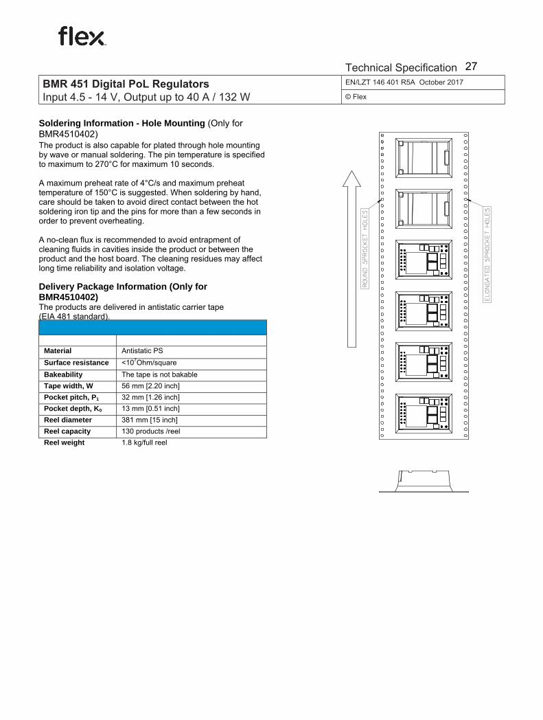
Soldering Information - Hole Mounting (Only for BMR4510402)The product is also capable for plated through hole mounting by wave or manual soldering. The pin temperature is specified to maximum to 270°C for maximum 10 seconds. A maximum preheat rate of 4°C/s and maximum preheat temperature of 150°C is suggested. When soldering by hand, care should be taken to avoid direct contact between the hot soldering iron tip and the pins for more than a few seconds in order to prevent overheating. A no-clean flux is recommended to avoid entrapment of cleaning fluids in cavities inside the product or between the product and the host board. The cleaning residues may affect long time reliability and isolation voltage. Delivery Package Information (Only for BMR4510402) The products are delivered in antistatic carrier tape (EIA 481 standard).
Carrier Tape Specifications Material Antistatic PS Surface resistance <107Ohm/square Bakeability The tape is not bakable Tape width, W 56 mm [2.20 inch] Pocket pitch, P1 32 mm [1.26 inch] Pocket depth, K0 13 mm [0.51 inch] Reel diameter 381 mm [15 inch] Reel capacity 130 products /reel Reel weight 1.8 kg/full reel
BMR 451 Digital PoL RegulatorsInput 4.5 - 14 V, Output up to 40 A / 132 W
EN/LZT 146 401 R5A October 2017
© Flex
Technical Specification 27
Ericsson Internal PRODUCT SPEC. 3 (4)
Prepared (also subject responsible if other) No.
EPEIHLI 5/1301- BMR 451 0402 Uen Approved Checked Date Rev Reference
SEC/D (Lisa Li) See §1 2015-05-18 A
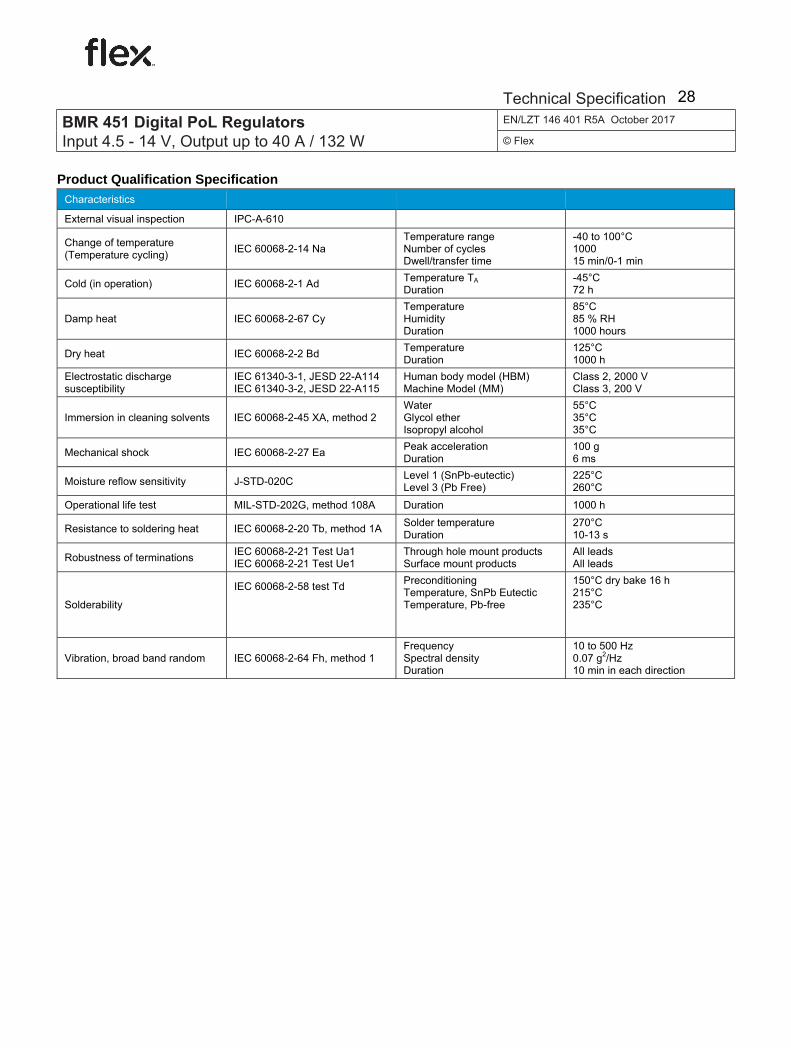
Product Qualification Specification
Characteristics
External visual inspection IPC-A-610
Change of temperature (Temperature cycling) IEC 60068-2-14 Na
Temperature range Number of cycles Dwell/transfer time
-40 to 100°C 1000 15 min/0-1 min
Cold (in operation) IEC 60068-2-1 Ad Temperature TA Duration
-45°C 72 h
Damp heat IEC 60068-2-67 Cy Temperature Humidity Duration
85°C 85 % RH 1000 hours
Dry heat IEC 60068-2-2 Bd Temperature Duration
125°C 1000 h
Electrostatic discharge susceptibility
IEC 61340-3-1, JESD 22-A114 IEC 61340-3-2, JESD 22-A115
Human body model (HBM) Machine Model (MM)
Class 2, 2000 V Class 3, 200 V
Immersion in cleaning solvents IEC 60068-2-45 XA, method 2 Water Glycol ether Isopropyl alcohol
55°C 35°C 35°C
Mechanical shock IEC 60068-2-27 Ea Peak acceleration Duration
100 g 6 ms
Moisture reflow sensitivity J-STD-020C Level 1 (SnPb-eutectic) Level 3 (Pb Free)
225°C 260°C
Operational life test MIL-STD-202G, method 108A Duration 1000 h
Resistance to soldering heat IEC 60068-2-20 Tb, method 1A Solder temperature Duration
270°C 10-13 s
Robustness of terminations IEC 60068-2-21 Test Ua1 IEC 60068-2-21 Test Ue1
Through hole mount products Surface mount products
All leads All leads
Solderability
IEC 60068-2-58 test Td
Preconditioning Temperature, SnPb Eutectic Temperature, Pb-free
150°C dry bake 16 h 215°C 235°C
Vibration, broad band random IEC 60068-2-64 Fh, method 1 Frequency Spectral density Duration
10 to 500 Hz 0.07 g2/Hz 10 min in each direction
BMR 451 Digital PoL RegulatorsInput 4.5 - 14 V, Output up to 40 A / 132 W
EN/LZT 146 401 R5A October 2017
© Flex
Technical Specification 28