Enhanced Photon Tunneling by Surface Plasmon–Phonon ...
8
B. Zhao George W. Woodruff School of Mechanical Engineering, Georgia Institute of Technology, Atlanta, GA 30332 Z. M. Zhang 1 Fellow ASME George W. Woodruff School of Mechanical Engineering, Georgia Institute of Technology, Atlanta, GA 30332 e-mail: [email protected] Enhanced Photon Tunneling by Surface Plasmon–Phonon Polaritons in Graphene/hBN Heterostructures Enhancing photon tunneling probability is the key to increasing the near-field radiative heat transfer between two objects. It has been shown that hexagonal boron nitride (hBN) and graphene heterostructures can enable plentiful phononic and plasmonic resonance modes. This work demonstrates that heterostructures consisting of a monolayer graphene on an hBN film can support surface plasmon–phonon polaritons that greatly enhance the photon tunneling and outperform individual structures made of either graphene or hBN. Both the thickness of the hBN films and the chemical potential of graphene can affect the tunneling probability, offering potential routes toward passive or active control of near- field heat transfer. The results presented here may facilitate the system design for near- field energy harvesting, thermal imaging, and radiative cooling applications based on two-dimensional materials. [DOI: 10.1115/1.4034793] Keywords: nanoscale heat transfer, 2D materials, nanophotonics, hybrid plasmonic polaritons 1 Introduction The well-known diffraction limit in optical imaging is caused by the disappearance of evanescent waves in the far field, which contain fine feature information of the sample surface and are critical for constructing images with high resolution [1]. The decay of the evanescent waves at large distances not only reduces the optical imaging resolution but also limits the radiative heat transfer between two objects in the far field. Thermal radiation is initiated by the fluctuational motion of charges inside materials at above absolute 0 K and contains both propagating and evanescent waves [2,3]. If the distance between two media is greater than the characteristic wavelength of thermal radiation, i.e., in the far field, only propagating waves generated by one medium can reach the other and contribute to radiative heat transfer. The disappearance of evanescent waves in the far field limits the radiative heat trans- fer to a rate that cannot exceed the blackbody limit governed by the well-known Stefan–Boltzmann law. The limited radiative heat transfer greatly hinders the application where thermal radiation plays a major role, such as radiative energy harvesting, thermal management, and local heating and cooling [3–8]. To overcome this limit, the evanescent waves have to be collected, which can be done by enabling photon tunneling. When two objects are at a distance comparable to or shorter than the characterized thermal radiation wavelength, i.e., in the near-field regime, the forward and backward evanescent waves can couple with each other and open paths for photons to tunnel through. This phenomenon is called photon tunneling and there are more tunneling photons than propagating photons, resulting in a radiative heat transfer rate that can be orders of magnitude higher than the blackbody limit. The huge radiative heat flux in the near field opens the door to various applications like thermal rectification [9], thermophotovoltaics [10,11], noncontact refrigeration [12], and information processing [13]. Since a large heat transfer is of critical importance in these appealing applica- tions, continuous efforts have been devoted to exploring innova- tive optical materials that can enhance photon tunneling. Surface modes, such as surface plasmon polaritons (SPPs) or surface phonon polaritons (SPhPs), have been demonstrated to mediate photon tunneling between metallic surfaces and polar materials [14,15]. Nanostructures like photonic crystals, nanowire arrays, and gratings could effectively behave as hyperbolic metamaterials, which support propagating waves with large wave vectors and thus enhance photon tunneling [16–19]. The two- dimensional (2D) materials can enable plentiful resonances [20–26] to facilitate photon tunneling. For example, graphene sup- ports SPPs that can enhance photon tunneling between graphene sheets [27,28]. Graphene SPPs can also couple with the hyper- bolic modes in nanowires, resulting in nearly perfect photon tun- neling [29]. When graphene is patterned to ribbons, hyperbolic plasmons can be excited that can significantly enhance photon tunneling than with continuous graphene [30,31]. As a natural hyperbolic material, hexagonal boron nitride (hBN) can support multiple orders of phonon–polaritonic waveguide modes in its two infrared Reststrahlen bands [32–34]. Recently, it has been demonstrated both theoretically and experimentally that van der Waals heterostructures assembled by graphene and hBN can sup- port surface plasmon–phonon polaritons (SPPPs), which are resulted from the strong coupling between the phonon polaritons in hBN and the surface plasmons in graphene [35–37]. It is still a question whether SPPPs can enhance photon tunneling between such heterostructures and enable a higher heat flux than other 2D materials like graphene. Meanwhile, since graphene has been pro- posed for a number of promising nano-electronic applications, and hBN is an ideal substrate supporting high-quality graphene owing to its planar hexagonal lattice structure [38,39], it is imper- ative to explore the effect of hBN on graphene regarding radiative heat transfer performance. The present study theoretically investigates the effect of SPPPs in enhancing the photon tunneling between graphene and hBN heterostructures. The near-field radiative heat transfer between the 1 Corresponding author. Contributed by the Heat Transfer Division of ASME for publication in the JOURNAL OF HEAT TRANSFER. Manuscript received May 9, 2016; final manuscript received August 30, 2016; published online October 18, 2016. Assoc. Editor: Alan McGaughey. Journal of Heat Transfer FEBRUARY 2017, Vol. 139 / 022701-1 Copyright V C 2017 by ASME Downloaded From: http://heattransfer.asmedigitalcollection.asme.org/ on 10/26/2016 Terms of Use: http://www.asme.org/about-asme/terms-of-use
Transcript of Enhanced Photon Tunneling by Surface Plasmon–Phonon ...

B. ZhaoGeorge W. Woodruff School
of Mechanical Engineering,
Georgia Institute of Technology,
Atlanta, GA 30332
Z. M. Zhang1
Fellow ASME
George W. Woodruff School
of Mechanical Engineering,
Georgia Institute of Technology,
Atlanta, GA 30332
e-mail: [email protected]
Enhanced Photon Tunnelingby Surface Plasmon–PhononPolaritons in Graphene/hBNHeterostructuresEnhancing photon tunneling probability is the key to increasing the near-field radiativeheat transfer between two objects. It has been shown that hexagonal boron nitride (hBN)and graphene heterostructures can enable plentiful phononic and plasmonic resonancemodes. This work demonstrates that heterostructures consisting of a monolayer grapheneon an hBN film can support surface plasmon–phonon polaritons that greatly enhance thephoton tunneling and outperform individual structures made of either graphene or hBN.Both the thickness of the hBN films and the chemical potential of graphene can affect thetunneling probability, offering potential routes toward passive or active control of near-field heat transfer. The results presented here may facilitate the system design for near-field energy harvesting, thermal imaging, and radiative cooling applications based ontwo-dimensional materials. [DOI: 10.1115/1.4034793]
Keywords: nanoscale heat transfer, 2D materials, nanophotonics, hybrid plasmonicpolaritons
1 Introduction
The well-known diffraction limit in optical imaging is causedby the disappearance of evanescent waves in the far field, whichcontain fine feature information of the sample surface and arecritical for constructing images with high resolution [1]. Thedecay of the evanescent waves at large distances not only reducesthe optical imaging resolution but also limits the radiative heattransfer between two objects in the far field. Thermal radiation isinitiated by the fluctuational motion of charges inside materials atabove absolute 0 K and contains both propagating and evanescentwaves [2,3]. If the distance between two media is greater than thecharacteristic wavelength of thermal radiation, i.e., in the far field,only propagating waves generated by one medium can reach theother and contribute to radiative heat transfer. The disappearanceof evanescent waves in the far field limits the radiative heat trans-fer to a rate that cannot exceed the blackbody limit governed bythe well-known Stefan–Boltzmann law. The limited radiative heattransfer greatly hinders the application where thermal radiationplays a major role, such as radiative energy harvesting, thermalmanagement, and local heating and cooling [3–8]. To overcomethis limit, the evanescent waves have to be collected, which canbe done by enabling photon tunneling.
When two objects are at a distance comparable to or shorterthan the characterized thermal radiation wavelength, i.e., in thenear-field regime, the forward and backward evanescent wavescan couple with each other and open paths for photons to tunnelthrough. This phenomenon is called photon tunneling and thereare more tunneling photons than propagating photons, resulting ina radiative heat transfer rate that can be orders of magnitudehigher than the blackbody limit. The huge radiative heat flux inthe near field opens the door to various applications like thermalrectification [9], thermophotovoltaics [10,11], noncontact
refrigeration [12], and information processing [13]. Since a largeheat transfer is of critical importance in these appealing applica-tions, continuous efforts have been devoted to exploring innova-tive optical materials that can enhance photon tunneling.
Surface modes, such as surface plasmon polaritons (SPPs) orsurface phonon polaritons (SPhPs), have been demonstrated tomediate photon tunneling between metallic surfaces and polarmaterials [14,15]. Nanostructures like photonic crystals, nanowirearrays, and gratings could effectively behave as hyperbolicmetamaterials, which support propagating waves with large wavevectors and thus enhance photon tunneling [16–19]. The two-dimensional (2D) materials can enable plentiful resonances[20–26] to facilitate photon tunneling. For example, graphene sup-ports SPPs that can enhance photon tunneling between graphenesheets [27,28]. Graphene SPPs can also couple with the hyper-bolic modes in nanowires, resulting in nearly perfect photon tun-neling [29]. When graphene is patterned to ribbons, hyperbolicplasmons can be excited that can significantly enhance photontunneling than with continuous graphene [30,31]. As a naturalhyperbolic material, hexagonal boron nitride (hBN) can supportmultiple orders of phonon–polaritonic waveguide modes in itstwo infrared Reststrahlen bands [32–34]. Recently, it has beendemonstrated both theoretically and experimentally that van derWaals heterostructures assembled by graphene and hBN can sup-port surface plasmon–phonon polaritons (SPPPs), which areresulted from the strong coupling between the phonon polaritonsin hBN and the surface plasmons in graphene [35–37]. It is still aquestion whether SPPPs can enhance photon tunneling betweensuch heterostructures and enable a higher heat flux than other 2Dmaterials like graphene. Meanwhile, since graphene has been pro-posed for a number of promising nano-electronic applications,and hBN is an ideal substrate supporting high-quality grapheneowing to its planar hexagonal lattice structure [38,39], it is imper-ative to explore the effect of hBN on graphene regarding radiativeheat transfer performance.
The present study theoretically investigates the effect of SPPPsin enhancing the photon tunneling between graphene and hBNheterostructures. The near-field radiative heat transfer between the
1Corresponding author.Contributed by the Heat Transfer Division of ASME for publication in the
JOURNAL OF HEAT TRANSFER. Manuscript received May 9, 2016; final manuscriptreceived August 30, 2016; published online October 18, 2016. Assoc. Editor: AlanMcGaughey.
Journal of Heat Transfer FEBRUARY 2017, Vol. 139 / 022701-1Copyright VC 2017 by ASME
Downloaded From: http://heattransfer.asmedigitalcollection.asme.org/ on 10/26/2016 Terms of Use: http://www.asme.org/about-asme/terms-of-use

heterostructures calculated based on fluctuational electrodynamicsis compared with the scenarios where only graphene monolayersor hBN films are present. The dispersion of the hybrid polaritonsin the heterostructure and their contributions to the near-field heattransfer are discussed. The effects of thickness of the hBN filmand the chemical potential of graphene on the dispersion areinvestigated. A second layer of graphene on the backside of theheterostructure is further explored for its impact on the dispersionand near-field heat transfer of the heterostructure.
2 Theory
Figure 1(a) shows the configuration of near-field radiative heattransfer between two aligned heterostructures separated by a vac-uum gap of d. Each heterostructure contains a monolayer gra-phene covered on an hBN film with a thickness denoted as h. Theupper one is the emitter with a relatively higher temperature T1
and the lower one is the receiver with a lower temperature T2.Graphene is modeled with a sheet conductivity, rs, that includesthe contributions from both the interband and intraband transitions[29]. In the mid- and far-infrared region, rs is dominated by theintraband transitions and can be approximately written as
rs ¼e2l
p�h2
s1� ixs
(1)
where e is the elementary charge, �h is the reduced Planck con-stant, x is the angular frequency, s is the relaxation time, and l isthe chemical potential [25]. Here, s ¼ 10�13 s is chosen for all thecalculations. Figures 2(a) and 2(b) show the real and imaginaryparts of rs with different chemical potentials, where r0 ¼ e2=4�h.The curves in Figs. 2(a) and 2(b) are almost identical with theprediction from Eq. (1), except for l ¼ 0:1 eV toward thehigh-frequency end where interband transitions becomeimportant.
The hBN film is a uniaxial crystal in the infrared region, whoseoptical axis lies in the z-direction, with two mid-infraredReststrahlen bands. The in-plane (when the electric field is per-pendicular to the optical axis) and out-of-plane (when theelectric field is parallel to the optical axis) dielectric functionsinclude the contribution from the in-plane phonon vibrations(xTO;? ¼ 1370 cm�1 and xLO;? ¼ 1610 cm�1) and out-of-planephonon vibrations (xTO;k ¼ 780 cm�1 and xLO;k ¼ 830 cm�1),respectively, as given by
em ¼ e1;m 1þx2
LO;m � x2TO;m
x2TO;m � icmx� x2
!(2)
where m¼ k;? [36]. The other parameters used are e1;k ¼ 2:95,
ck ¼ 4 cm�1, e1;? ¼ 4:87, and c? ¼ 5 cm�1. According to
Eq. (2), for small damping coefficient c, the dielectric functionbecomes negative in Reststrahlen band between the TO and LOphonon modes. Therefore, the in-plane and out-of-plane dielectric
Fig. 1 (a) Schematic of near-field radiative heat transferbetween two graphene/hBN heterostructures. (b) Illustration ofthe regions for calculating the reflection coefficients.
Fig. 2 Sheet conductivity of graphene with different chemicalpotentials: (a) real part and (b) imaginary part. The values arenormalized by r0 5 e2=4�h. (c) Real part of the dielectric functionof hBN. The shaded areas indicate the two hyperbolic regionsof hBN.
022701-2 / Vol. 139, FEBRUARY 2017 Transactions of the ASME
Downloaded From: http://heattransfer.asmedigitalcollection.asme.org/ on 10/26/2016 Terms of Use: http://www.asme.org/about-asme/terms-of-use
functions of hBN possess opposite signs in either Reststrahlenband. As a result, the isofrequency contour becomes hyperbolic inthese regions, making hBN a natural hyperbolic metamaterial.Figure 2(c) shows the real part of the dielectric function of hBNand the two hyperbolic regions are marked by the shaded areas.
The near-field radiative heat flux q is calculated based on fluc-tuational electrodynamics using dyadic Green’s functions [2]
q ¼ 1
4p2
ð10
H x;T1ð Þ �H x; T2ð Þ½ �ð1
0
n x; bð Þbdb
� �dx (3)
where H(x,T) is the average energy of a Planck oscillator, bdesignates the magnitude of the wavevector in the x–y plane,and nðx; bÞ is the photon tunneling probability (also calledenergy transmission coefficient). The photon tunnelingprobability includes contributions of both the transverse electric(TE) waves (or s-polarization) and transverse magnetic (TM)waves (or p-polarization), that is, nðx;bÞ ¼ nsðx;bÞþ npðx;bÞ.Here
nj x; bð Þ ¼
1� jrjj2� �2
j1� r2j e2ikz0dj2
; b < k0
4 Im rjð Þ� �2e�2jkz0jd
j1� r2j e2ikz0dj2
; b > k0
8>>>>>>><>>>>>>>:
(4)
where j is for either s or p polarization, rj signifies the correspond-ing reflection coefficient, and Im takes the imaginary part [18].The magnitude and z-component of the wavevector in vacuum aredenoted as k0 and kz0, respectively.
The reflection coefficient of TM waves for the graphene/hBNheterostructure takes the following form:
rp ¼r12;p þ 1� r12;p � r21;pð Þr23;p exp 2ikz;2hð Þ
1� r21;pr23;p exp 2ikz;2hð Þ(5)
where 1, 2, and 3 are the indexes for the vacuum region abovehBN film, the hBN film region, and the vacuum region belowhBN film, respectively, as defined in Fig. 1(b). Also, the reflectioncoefficient between the vacuum and hBN or vice versa can beobtained by
rab;p ¼
e?;bkz;b� e?;a
kz;aþ rs
xe0
e?;bkz;bþ e?;a
kz;aþ rs
xe0
(6a)
if there is a graphene layer in between media a and b, where a¼ 1or 2 and b¼ 1, 2 or 3. The effect of graphene is included asa current sheet. If there is no graphene in between media a and b,then
rab;p ¼
e?;bkz;b� e?;a
kz;ae?;bkz;bþ e?;a
kz;a
(6b)
In Eqs. (6a) and (6b), e0 is the vacuum permittivity and
kz;b ¼ ðe?;bk20 � e?;bb
2=ek;bÞ1=2with b being 1, 2 or 3 in Eqs. (5)
and (6) is the z-component of the wavevector in a givenregion. For regions with isotropic medium like regions 1 and 3,e1 ¼ e3 ¼ e? ¼ ek ¼ 1. For TE waves, the reflection coefficient
can be expressed as
rs ¼r12;s þ 1þ r12;s þ r21;sð Þr23;s exp 2ikz;2hð Þ
1� r21;sr23;s exp 2ikz;2hð Þ(7)
where
rab;s ¼
kz;a
la
� rsxl0 �kz;b
lb
kz;a
la
þ rsxl0 þkz;b
lb
; with a graphene sheet (8a)
and
rab;s ¼
kz;a
la
� kz;b
lb
kz;a
la
þ kz;b
lb
; without a graphene sheet (8b)
Here, l0 is the permeability of vacuum and lb (b¼ 1, 2 or 3) isthe relative permeability for region b, which is unity for allregions since the materials are all nonmagnetic. Note that inEqs. (7) and (8), kz;b ¼ ðe?;bk2
0 � b2Þ1=2since TE waves are ordi-
nary waves in the hBN film. As mentioned before, the near-fieldradiative heat transfer is dominated by TM waves. Equations (5)and (7) can also be used for structures with only graphene by set-ting r23 ¼ 0. They can also be used for the structure without gra-phene, with one graphene sheet as shown in Fig. 1, or with agraphene monolayer on both sides of the hBN film to be discussedlater. An alternative method can also be used is to treat graphenesheet as a layer of thickness D¼ 0.3 nm with an effective dielec-tric function eeff ¼ 1þ irs=ðe0xDÞ [40]. Both methods yieldessentially identical results with less than 0.5% in the predictedtotal heat flux. The analytical expressions of the reflection coeffi-cients presented here not only help elucidate the fundamentalmechanisms of the coupled plasmonic resonances (to be discussedlater) but also can save a lot of simulation time once implanted inthe numerical algorithm.
3 Results and Discussion
Figure 3 compares the heat fluxes between a pair of graphenesheets, hBN films with h¼ 50 nm, and the heterostructures shownin Fig. 1(a). The chemical potential of graphene is set to 0.37 eV,according to a previous experiment [37]. In the calculations, thetemperatures of the emitter and receiver are set as T1¼ 300 Kand T2¼ 0 K, respectively. However, the optical properties of
Fig. 3 Comparison of the radiative heat flux as a function ofgap spacing d between the heterostructures shown in Fig. 1(a),graphene monolayers (same structures without the hBNfilm), and hBN films (same structures without graphene). Thetemperatures of the emitter and receiver are set at 300 and 0 K,respectively. The film thickness is h 5 50 nm and the chemicalpotential of graphene is l 5 0.37 eV.
Journal of Heat Transfer FEBRUARY 2017, Vol. 139 / 022701-3
Downloaded From: http://heattransfer.asmedigitalcollection.asme.org/ on 10/26/2016 Terms of Use: http://www.asme.org/about-asme/terms-of-use

graphene and hBN are evaluated at room temperature of 300 K. Interms of the radiative heat flux, the heterostructure outperformsthe other configurations, especially at small gap distances. Atd¼ 10 nm, the heterostructure yields q¼ 800 kW/m2 that is morethan twice of that between graphene monolayers or hBN films,which are 305 and 212 kW/m2, respectively. When d exceedsabout 200 nm, the heat flux for the heterostructures is very closeto that between suspended graphene sheets, indicating a negligibleeffect of the hBN film. Note that the radiative heat flux betweenblackbodies (in the far field) is 459 W/m2, which is orders of mag-nitude smaller than the near-field heat flux shown in Fig. 3.
The mechanism for the enhanced heat transfer between theheterostructures can be elucidated by the contours of photon tun-neling probability displayed in Fig. 4 for the three scenarios. Notethat for the structures considered in this work, np � ns since thepolaritons discussed here can only be excited for TM waves,which are the dominating contribution to the near-field radiativeflux. The bright bands shown in Fig. 4 indicate efficient photontunneling due to the excitation of different polaritons, correspond-ing to the dispersion curves where the denominator of np inEq. (4) approaches zero. The two bands in Fig. 4(a) correspond tothe symmetric (lower frequencies) and asymmetric (higher fre-quencies) branches of the coupled SPPs between two graphenesheets. They are the major contributors to the high near-field heatflux between graphene [30]. For hBN films shown in Fig. 4(b),multiple phononic waveguide modes can be identified in eachReststrahlen band between the horizontal dashed lines. However,there exist strong tunneling branches outside the two Reststrahlenbands for the heterostructure, as shown in Fig. 4(c). These addi-tional polaritons, identified as SPPPs, are one kind of hybridpolaritons resulted from the coupling between surface plasmons ingraphene and phonon polaritons in hBN [36,37]. Note that similarto the Fig. 4(a), each order of the polariton bands in Figs. 4(b) and4(c) splits into two branches. The mechanism of hybrid polaritonsand their impact on near-field radiative transfer are elaborated inthe following.
The hybrid polaritons in the heterostructure can be categorizedinto two kinds depending on whether they are inside or outsidethe Reststrahlen band of hBN. Specifically, the dispersion of thehybrid polaritons takes two expressions based on the dielectricfunction of hBN [36]
b xð Þ
¼
�dh
npþarctanxe0e1þibrs
dxe0e?;2
� þarctan
e3
de?;2
� " #; e?;2ek;2<0
jdj2h
lnxe0e1�xe0e?;2jdjþibrs
xe0e1þxe0e?;2jdjþibrs
�e3�e?;2jdje3þe?;2jdj
!; e?;2ek;2>0
8>>>>><>>>>>:
(9)
When e?;2ek;2 < 0, the isofrequency contour of hBN is hyperbolic
and the hybrid polaritons are referred to as hyperbolicplasmon–phonon polaritons (HPPPs) [37] since they preservethe hyperbolic-waveguide-mode features as in an uncoveredhBN film. Integer n denotes the resonance order. Here,
d ¼ 6iffiffiffiffiffiffiffiffiffiffiffiffiffiffiffiffiffiek;2=e?;2
pand the plus or minus sign is chosen based on
the shape of the HPPPs bands [36]. If rs is set to zero, the firstexpression in Eq. (9) recovers the dispersion for the waveguidemodes in hBN films. When e?;2ek;2 > 0, the isofrequency contour
of hBN becomes elliptic, and SPPPs can be supported in the threefrequency regions below, between, and above the two Reststrah-len bands, as shown in Fig. 4(c). Unlike HPPPs, SPPPs are surfacemodes with a strong plasmonic characteristic when they are not soclose to the Reststrahlen bands [37]. If rs is set to zero (i.e., with-out graphene), the second expression in Eq. (9) yields a negativeb since e?;2 > 0, suggesting that hBN films cannot support anyresonances outside the two Reststrahlen bands. This provides an
explanation why the resonances only exist within the Reststrahlenbands as Fig. 4(b) shows.
It is worth pointing out that the second expression in Eq. (9)does not require an anisotropic substrate to yield a valid solution.Thus, phononic polaritons in films made of isotropic polar materi-als like SiO2 and SiC could also couple with SPPs in graphene toform a hybridized polariton, whose dispersion can be obtained by
Fig. 4 Photon tunneling probability contours for differentstructures: (a) graphene monolayers, (b) hBN films, and (c) het-erostructures shown in Fig. 1(a). The dashed lines indicate thetwo Reststrahlen bands of hBN. The parameters are d 5 20 nm,h 5 50 nm, and l 5 0.37 eV.
022701-4 / Vol. 139, FEBRUARY 2017 Transactions of the ASME
Downloaded From: http://heattransfer.asmedigitalcollection.asme.org/ on 10/26/2016 Terms of Use: http://www.asme.org/about-asme/terms-of-use
setting jdj ¼ 1. Similar phenomena were demonstrated for thecoupling between SPPs in graphene or thin metal layer with theSPhPs supported by semi-infinite polar material substrates[41,42]. Moreover, a prominent feature that can be identified inFig. 4(c) is the mode flatting when the SPPPs approach eitherReststrahlen band near xTO. This is caused by the anticrossingeffect or mode repulsion between SPPs in graphene and wave-guide modes in hBN, and same effect was found to exist betweenSPPs in a thin metal layer and SPhPs in isotropic polar substrates[41]. Because of this effect, the two hyperbolic Reststrahlen bandsbreak the otherwise continuous SPPPs into three regions in fre-quency, allowing high density of state to occur at some bandedges and boosting the photon tunneling, as will be discussed inthe next.
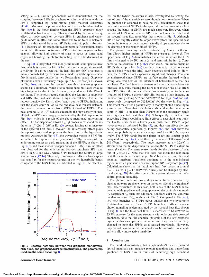
If Eq. (3) is integrated over b only, the result is the spectral heatflux, which is shown in Fig. 5 for the three configurations withd¼ 20 nm. It can be seen that the heat flux for hBN structures ismainly contributed by the waveguide modes, and the spectral heatflux is nearly zero outside the two Reststrahlen bands. Grapheneplasmons cover a frequency range up to 6� 1014 rad=s as shownin Fig. 4(a), and thus the spectral heat flux between graphenesheets has a nontrivial value over a broad band but fades away athigh frequencies due to the frequency dependence of the Planckoscillator. The heterostructure combines the features of grapheneand hBN film, and also shows a high spectral heat flux in theregions outside the Reststrahlen bands due to SPPPs, indicatingthat the major contribution to the radiative heat transfer betweenthe heterostructures comes from SPPPs instead of HPPPs. Thepeak around 1:4� 1014 rad=s is caused by the high density of state[43] of the SPPPs near xTO;k, as indicated by the flat dispersion inFig. 4(c), which is a result of the above-mentioned anticrossingeffect. The flat dispersion allows high b modes to exist and makesthe term
Ð10
nðx;bÞbdb in Eq. (3) greater, leading to an increasein the spectral heat flux. However, the anticrossing effect playsthe opposite role and suppresses the heat flux in the hyperbolicregions. As shown in Fig. 4(b), the waveguide modes in hBN filmare able to be supported when b is about 150k0. In contrast, theanticrossing causes an early truncation of the HPPPs, as shown inFig. 4(c), and these modes disappear at about 100k0. Similar effectwas observed for the anticrossing between graphene SPPs andSPhPs in SiC and SiO2, where SPPs truncate the SPhPs at largewavevectors [42,44]. This early truncation results in a lower spec-tral heat flux for the heterostructures in the two hyperbolic bandscompared to the hBN films, as indicated in Fig. 5. The effect of
loss on the hybrid polaritons is also investigated by setting theloss of one of the materials to zero, though not shown here. Whenthe graphene is assumed to have no loss, calculations show thatthe contribution of SPPPs to the spectral flux becomes much lessbecause the bands of SPPPs are much narrower. However, whenthe loss of hBN is set to zero, SPPPs are not much affected andthe spectral heat flux resembles that shown in Fig. 5. AlthoughHPPPs can slightly extend to larger wavevectors, the spectral heatflux in the two hyperbolic regions actually drops somewhat due tothe decrease of the bandwidth of HPPPs.
The photon tunneling can be controlled by h since a thickerfilm allows higher orders of HPPPs to present at lower b. Theupper panel of Fig. 6 demonstrates this effect, in which the hBNfilm is changed to be 200 nm in (a) and semi-infinite in (b). Com-pared to the scenario in Fig. 4(c) when h¼ 50 nm, more orders ofHPPPs show up in Fig. 6(a) and they eventually merge to a con-tinuous band when the hBN layer becomes semi-infinite. How-ever, the SPPPs do not experience significant changes. This canbe understood since SPPPs are surface modes featured with astrong localized field on the interface of heterostructure that hasgraphene. The field intensity evanescently decays away from theinterface and, thus, making the hBN film thicker has little effecton SPPPs. Since the enhanced heat flux is mainly due to the con-tribution of SPPPs, a thicker hBN film brings a slight increase inthe heat flux, yielding 537 and 547 kW/m2 for Figs. 6(a) and (b),respectively, compared to 513 kW/m2 for the case in Fig. 4(c).This effect may offer a passive way to modify photon tunneling tosome extent. Note that calculations show that the penetrationdepth in hBN is smaller than 300 nm over the frequency rangewith high spectral heat flux [45]. Subsequently, a thicker filmexceeding 300 nm would have little effect to near-field heat trans-fer. On the other hand, a lower l can push the SPPPs to largerwavevectors as indicated by Eq. (9), and thus can affect the tun-neling probability significantly. Figures 6(c) and 6(d) show thetunneling probability when l is changed to 0.2 and 0.6 eV, respec-tively. The SPPP bands become flatter in (c) and steeper in (d)compared to Fig. 4(c), and thus, q becomes 1131 kW/m2 and249 kW/m2, respectively. The huge increase at l¼ 0.2 eV isattributed to the flat dispersion that allows the SPPPs to extend tolarger b values. The same reason holds for the decrease of heatflux at l¼ 0.6 eV. Note that this does not mean the maximumheat flux can be achieved at l¼ 0 eV because at this chemicalpotential, interband transitions dominate rs in the near-infraredregion in which graphene does not support SPPs anymore [46,47].Calculations show that the maximum heat flux occurs at aroundl¼ 0.1 eV with q¼ 1700 kW/m2. Since l can be changed by elec-trical gating [20], this effect may offer a potential way to activelycontrol photon tunneling.
The photon tunneling probability can be further enhanced byplacing an extra graphene layer on the other side of the graphene/hBN heterostructure. In this case, both sides of the hBN film arecovered with graphene and the graphene on the backside can mod-ify coefficient r23 such that additional solutions exist that can zerothe denominator of np, as shown in Fig. 7. Compared to Fig. 4(c),two new branches of SPPPs occur outside the two hyperbolicReststrahlen bands. These SPPP branches further enhancephoton tunneling as demonstrated by the spectral heat flux shownin Fig. 8, and the total heat flux q is increased to 643 kW/m2 (a25.3% increase for the same structure with only one side coveredgraphene). Note that the chemical potentials of the two graphenelayers in this example are the same and they can be activelychanged to tune the SPPPs as discussed previously. However,they do not have to be the same and may be controlled independ-ently to allow more active tunability.
4 Conclusions
The work demonstrates that graphene/hBN heterostructuredoptical materials can enhance photon tunneling and outperformgraphene or hBN film in terms of achieving high near-field
Fig. 5 Spectral heat flux between two graphene monolayers,hBN films, and graphene/hBN heterostructures. The parametersused are the same as for Fig. 3.
Journal of Heat Transfer FEBRUARY 2017, Vol. 139 / 022701-5
Downloaded From: http://heattransfer.asmedigitalcollection.asme.org/ on 10/26/2016 Terms of Use: http://www.asme.org/about-asme/terms-of-use

Fig. 6 Photon tunneling probability contours for different graphene/hBN heterostructures.The gap distance is fixed at 20 nm and the other parameters are as follows: (a) h 5 200 nm andl 5 0.37 eV; (b) h 5 1‘ (semi-infinite) and l 5 0.37 eV; (c) h 5 50 nm and l 5 0.2 eV; and (d)h 5 50 nm and l 5 0.6 eV.
Fig. 7 Photon tunneling probability contour for the graphene/hBN/graphene heterostructure
Fig. 8 Comparison of the spectral heat flux for the graphene/hBN and graphene/hBN/graphene structures. The parametersare d 5 20 nm, h 5 50 nm, and l 5 0.37 eV.
022701-6 / Vol. 139, FEBRUARY 2017 Transactions of the ASME
Downloaded From: http://heattransfer.asmedigitalcollection.asme.org/ on 10/26/2016 Terms of Use: http://www.asme.org/about-asme/terms-of-use

radiative heat transfer, thanks to the hybrid mode SPPPs. TheSPPPs enhance the spectral heat flux outside the two Reststrahlenbands and can be controlled by the thickness of the hBN film andthe chemical potential of graphene. Placing an additional gra-phene layer on the other side of the hBN film further enhances theheat transfer between the heterostructures by allowing extra SPPPbranches. The findings in this work may facilitate the design ofsystems utilizing near-field thermal radiation with passively andactively tunable photon tunneling based on graphene and hBN.
Acknowledgment
This work was supported by the National Science Foundation(CBET-1235975; CBET-1603761).
Nomenclature
d ¼ vacuum gap width (m)e ¼ charge of an electron (1.602 � 10�19 C)h ¼ film thickness (m)�h ¼ reduced Planck’s constant (1.055 � 10�34 J�s)i ¼
ffiffiffiffiffiffiffi�1p
k0 ¼ wavevector in vacuum (m�1)kz0 ¼ z-component of the wavevector in vacuum (m�1)
n ¼ resonance orderq ¼ heat flux (W/m2)r ¼ reflection coefficientT ¼ temperature (K)
Greek Symbols
b ¼ magnitude of the wavevector in the x–y plane (m�1)c ¼ scattering rate (rad/s)d ¼ variable defined in Eq. (9)e ¼ dielectric function
e0 ¼ vacuum permittivity (8.854� 10�12 F�m�1)H ¼ mean energy of the Planck oscillator (J)l ¼ relative permeability or chemical potential (eV)
l0 ¼ permeability of vacuum (4p� 10�7 H�m�1)n ¼ photon tunneling probability
rs ¼ sheet conductivity (S)s ¼ relaxation time (s)x ¼ angular frequency (rad�s�1)
Subscripts
a, b, j, m ¼ indexeseff ¼ effectiveLO ¼ longitudinal optical phonon modes
p ¼ p-polarization or TM wavess ¼ s-polarization or TE waves
TO ¼ transverse optical phonon mode1, 2, 3 ¼ indexes for different regions? ¼ perpendicular to the optical axis|| ¼ parallel to the optical axis
References[1] Zhang, X., and Liu, Z., 2008, “Superlenses to Overcome the Diffraction Limit,”
Nat. Mater., 7(6), pp. 435–441.[2] Zhang, Z. M., 2007, Nano/Microscale Heat Transfer, McGraw-Hill, New York.[3] Liu, X. L., Wang, L. P., and Zhang, Z. M., 2015, “Near-Field Thermal
Radiation: Recent Progress and Outlook,” Nanoscale Microscale Thermophys.Eng., 19(2), pp. 98–126.
[4] Kim, K., Song, B., Fern�andez-Hurtado, V., Lee, W., Jeong, W., Cui, L.,Thompson, D., Feist, J., Reid, M. T. H., Garc�ıa-Vidal, F. J., Cuevas, J. C.,Meyhofer, E., and Reddy, P., 2015, “Radiative Heat Transfer in the ExtremeNear Field,” Nature, 528(7582), pp. 387–391.
[5] Basu, S., Zhang, Z. M., and Fu, C. J., 2009, “Review of Near-Field ThermalRadiation and Its Application to Energy Conversion,” Int. J. Energy Res.,33(13), pp. 1203–1232.
[6] Jones, A. C., and Raschke, M. B., 2012, “Thermal Infrared Near-FieldSpectroscopy,” Nano Lett., 12(3), pp. 1475–1481.
[7] De Wilde, Y., Formanek, F., Carminati, R., Gralak, B., Lemoine, P.-A., Joulain,K., Mulet, J.-P., Chen, Y., and Greffet, J.-J., 2006, “Thermal Radiation Scan-ning Tunnelling Microscopy,” Nature, 444(7120), pp. 740–743.
[8] Yang, Y., Basu, S., and Wang, L. P., 2013, “Radiation-Based Near-FieldThermal Rectification With Phase Transition Materials,” Appl. Phys. Lett.,103(16), p. 163101.
[9] Otey, C. R., Lau, W. T., and Fan, S., 2010, “Thermal Rectification ThroughVacuum,” Phys. Rev. Lett., 104(15), p. 154301.
[10] Park, K., Basu, S., King, W. P., and Zhang, Z. M., 2008, “Performance Analysisof Near-Field Thermophotovoltaic Devices Considering Absorption Distribu-tion,” J. Quant. Spectrosc. Radiat. Transfer, 109(2), pp. 305–316.
[11] Messina, R., and Ben-Abdallah, P., 2013, “Graphene-Based Photovoltaic Cellsfor Near-Field Thermal Energy Conversion,” Sci. Rep., 3, p. 1383.
[12] Chen, K., Santhanam, P., Sandhu, S., Zhu, L., and Fan, S., 2015, “Heat-FluxControl and Solid-State Cooling by Regulating Chemical Potential of Photonsin Near-Field Electromagnetic Heat Transfer,” Phys. Rev. B, 91(13), p. 134301.
[13] Ben-Abdallah, P., and Biehs, S.-A., 2014, “Near-Field Thermal Transistor,”Phys. Rev. Lett., 112(4), p. 044301.
[14] Basu, S., Lee, B. J., and Zhang, Z. M., 2010, “Near-Field Radiation CalculatedWith an Improved Dielectric Function Model for Doped Silicon,” ASME J.Heat Transfer, 132(2), p. 023302.
[15] Shen, S., Narayanaswamy, A., and Chen, G., 2009, “Surface Phonon PolaritonsMediated Energy Transfer Between Nanoscale Gaps,” Nano Lett., 9(8),pp. 2909–2913.
[16] Biehs, S. A., Tschikin, M., and Ben-Abdallah, P., 2012, “Hyperbolic Metamate-rials as an Analog of a Blackbody in the Near Field,” Phys. Rev. Lett., 109(10),p. 104301.
[17] Guo, Y., Cortes, C. L., Molesky, S., and Jacob, Z., 2012, “Broadband Super-Planckian Thermal Emission From Hyperbolic Metamaterials,” Appl. Phys.Lett., 101(13), p. 131106.
[18] Liu, X. L., Zhang, R. Z., and Zhang, Z. M., 2014, “Near-Field Radiative HeatTransfer With Doped-Silicon Nanostructured Metamaterials,” Int. J. Heat MassTransfer, 73, pp. 389–398.
[19] Poddubny, A., Iorsh, I., Belov, P., and Kivshar, Y., 2013, “Hyperbolic Meta-materials,” Nat. Photonics, 7(12), pp. 948–957.
[20] Grigorenko, A. N., Polini, M., and Novoselov, K. S., 2012, “GraphenePlasmonics,” Nat. Photonics, 6(11), pp. 749–758.
[21] Geim, A. K., and Grigorieva, I. V., 2013, “Van der Waals Heterostructures,”Nature, 499(7459), pp. 419–425.
[22] Xu, M., Liang, T., Shi, M., and Chen, H., 2013, “Graphene-LikeTwo-Dimensional Materials,” Chem. Rev., 113(5), pp. 3766–3798.
[23] Wang, F., Wang, Z., Wang, Q., Wang, F., Yin, L., Xu, K., Huang, Y., and He,J., 2015, “Synthesis, Properties and Applications of 2D Non-GrapheneMaterials,” Nanotechnol., 26(29), p. 292001.
[24] Xia, F., Wang, H., Xiao, D., Dubey, M., and Ramasubramaniam, A., 2014,“Two-Dimensional Material Nanophotonics,” Nat. Photonics, 8(12),pp. 899–907.
[25] Zhao, B., and Zhang, Z. M., 2015, “Strong Plasmonic Coupling BetweenGraphene Ribbon Array and Metal Gratings,” ACS Photonics, 2(11),pp. 1611–1618.
[26] Lim, M., Lee, S. S., and Lee, B. J., 2013, “Near-Field Thermal RadiationBetween Graphene-Covered Doped Silicon Plates,” Opt. Express, 21(19),pp. 22173–22185.
[27] Ilic, O., Jablan, M., Joannopoulos, J. D., Celanovic, I., Buljan, H., and Soljacic,M., 2012, “Near-Field Thermal Radiation Transfer Controlled by Plasmons inGraphene,” Phys. Rev. B, 85(15), p. 155422.
[28] Drosdoff, D., Phan, A. D., and Woods, L. M., 2014, “Transverse Electric Modefor Near-Field Radiative Heat Transfer in Graphene–Metamaterial Systems,”Adv. Opt. Mater., 2(11), pp. 1038–1042.
[29] Liu, X. L., Zhang, R. Z., and Zhang, Z. M., 2014, “Near-Perfect PhotonTunneling by Hybridizing Graphene Plasmons and Hyperbolic Modes,” ACSPhotonics, 1(9), pp. 785–789.
[30] Liu, X. L., and Zhang, Z. M., 2015, “Giant Enhancement of Nanoscale ThermalRadiation Based on Hyperbolic Graphene Plasmons,” Appl. Phys. Lett.,107(14), p. 143114.
[31] Liu, B., Liu, Y., and Shen, S., 2014, “Thermal Plasmonic Interconnects in Gra-phene,” Phys. Rev. B, 90(19), p. 195411.
[32] Lin, Y., and Connell, J. W., 2012, “Advances in 2D Boron Nitride Nanostruc-tures: Nanosheets, Nanoribbons, Nanomeshes, and Hybrids With Graphene,”Nanoscale, 4(22), pp. 6908–6939.
[33] Dai, S., Fei, Z., Ma, Q., Rodin, A. S., Wagner, M., McLeod, A. S., Liu, M. K.,Gannett, W., Regan, W., Watanabe, K., Taniguchi, T., Thiemens, M., Domi-nguez, G., Neto, A. H. C., Zettl, A., Keilmann, F., Jarillo-Herrero, P., Fogler,M. M., and Basov, D. N., 2014, “Tunable Phonon Polaritons in AtomicallyThin van der Waals Crystals of Boron Nitride,” Science, 343(6175),pp. 1125–1129.
[34] Jacob, Z., 2014, “Nanophotonics: Hyperbolic Phonon–Polaritons,” Nat. Mater.,13(12), pp. 1081–1083.
[35] Brar, V. W., Jang, M. S., Sherrott, M., Kim, S., Lopez, J. J., Kim, L. B., Choi,M., and Atwater, H., 2014, “Hybrid Surface-Phonon–Plasmon Polariton Modesin Graphene/Monolayer h-BN Heterostructures,” Nano Lett., 14(7),pp. 3876–3880.
[36] Kumar, A., Low, T., Fung, K. H., Avouris, P., and Fang, N. X., 2015, “TunableLight–Matter Interaction and the Role of Hyperbolicity in Graphene–hBN Sys-tem,” Nano Lett., 15(5), pp. 3172–3180.
[37] Dai, S., Ma, Q., Liu, M. K., Andersen, T., Fei, Z., Goldflam, M. D., Wagner,M., Watanabe, K., Taniguchi, T., Thiemens, M., Keilmann, F., Janssen,
Journal of Heat Transfer FEBRUARY 2017, Vol. 139 / 022701-7
Downloaded From: http://heattransfer.asmedigitalcollection.asme.org/ on 10/26/2016 Terms of Use: http://www.asme.org/about-asme/terms-of-use

G. C. A. M., Zhu, S. E., Jarillo Herrero, P., Fogler, M. M., and Basov, D. N.,2015, “Graphene on Hexagonal Boron Nitride as a Tunable Hyperbolic Meta-material,” Nat. Nanotechnol., 10(8), pp. 682–686.
[38] Dean, C. R., Young, A. F., Meric, I., Lee, C., Wang, L., Sorgenfrei, S., Wata-nabe, K., Taniguchi, T., Kim, P., Shepard, K. L., and Hone, J., 2010, “BoronNitride Substrates for High-Quality Graphene Electronics,” Nat. Nanotechnol.,5(10), pp. 722–726.
[39] Yan, Z., Chen, L., Yoon, M., and Kumar, S., 2016, “Phonon Transport at theInterfaces of Vertically Stacked Graphene and Hexagonal Boron NitrideHeterostructures,” Nanoscale, 8(7), pp. 4037–4046.
[40] Vakil, A., and Engheta, N., 2011, “Transformation Optics Using Graphene,”Science, 332(6035), pp. 1291–1294.
[41] Dubois, L. H., Schwartz, G. P., Camley, R. E., and Mills, D. L., 1984, “InelasticScattering of Electrons From Ionic Crystals With a Highly Conducting Over-layer,” Phys. Rev. B, 29(6), pp. 3208–3216.
[42] Messina, R., Hugonin, J.-P., Greffet, J.-J., Marquier, F., De Wilde, Y., Belar-ouci, A., Frechette, L., Cordier, Y., and Ben-Abdallah, P., 2013, “Tuning the
Electromagnetic Local Density of States in Graphene-Covered Systems ViaStrong Coupling With Graphene Plasmons,” Phys. Rev. B, 87(8), p. 085421.
[43] Jones, A. C., O’Callahan, B. T., Yang, H. U., and Raschke, M. B., 2013, “TheThermal Near-Field: Coherence, Spectroscopy, Heat-Transfer, and OpticalForces,” Prog. Surf. Sci., 88(4), pp. 349–392.
[44] Liu, X. L., and Zhang, Z. M., 2014, “Graphene-Assisted Near-Field RadiativeHeat Transfer Between Corrugated Polar Materials,” Appl. Phys. Lett.,104(25), p. 251911.
[45] Bright, T. J., Liu, X. L., and Zhang, Z. M., 2014, “Energy Streamlines in Near-Field Radiative Heat Transfer Between Hyperbolic Metamaterials,” Opt.Express, 22(S4), pp. A1112–A1127.
[46] Zhao, B., Zhao, J. M., and Zhang, Z. M., 2014, “Enhancement of Near-InfraredAbsorption in Graphene With Metal Gratings,” Appl. Phys. Lett., 105(3),p. 031905.
[47] Zhao, B., Zhao, J. M., and Zhang, Z. M., 2015, “Resonance Enhanced Absorp-tion in a Graphene Monolayer Using Deep Metal Gratings,” J. Opt. Soc. Am. B,32(6), pp. 1176–1185.
022701-8 / Vol. 139, FEBRUARY 2017 Transactions of the ASME
Downloaded From: http://heattransfer.asmedigitalcollection.asme.org/ on 10/26/2016 Terms of Use: http://www.asme.org/about-asme/terms-of-use