ENHANCED LIGHT OUTPUT FROM LUMINSECENT OXIDE …
119
1 ENHANCED LIGHT OUTPUT FROM LUMINSECENT OXIDE NANOPARTICLES: SYNTHESIS, CHARACTERIZATION AND SCINTILLATION APPLICATION By JIHUN CHOI A DISSERTATION PRESENTED TO THE GRADUATE SCHOOL OF THE UNIVERSITY OF FLORIDA IN PARTIAL FULFILLMENT OF THE REQUIREMENTS FOR THE DEGREE OF DOCTOR OF PHILOSOPHY UNIVERSITY OF FLORIDA 2011
Transcript of ENHANCED LIGHT OUTPUT FROM LUMINSECENT OXIDE …
1
ENHANCED LIGHT OUTPUT FROM LUMINSECENT OXIDE NANOPARTICLES: SYNTHESIS, CHARACTERIZATION AND SCINTILLATION APPLICATION
By
JIHUN CHOI
A DISSERTATION PRESENTED TO THE GRADUATE SCHOOL OF THE UNIVERSITY OF FLORIDA IN PARTIAL FULFILLMENT
OF THE REQUIREMENTS FOR THE DEGREE OF DOCTOR OF PHILOSOPHY
UNIVERSITY OF FLORIDA
2011

2
© 2011 Jihun Choi

3
To my wife, my son and my parents

4
ACKNOWLEDGMENTS
I would never have been able to finish my dissertation without the guidance of my
committee members, help from our group members, and support from my family.
I would like to express my deepest gratitude to my advisor, Dr. Paul H. Holloway,
for his excellent guidance, caring, patience, and providing me with an excellent
atmosphere for research. His countless passion and endless effort to pursue knowledge
always made me refreshed and motivated, and his logical attitude toward science has
reinforced my perception about research. I also would like to thank my supervisory
committee; Dr. Mark Davidson, Dr. Rolf Hummel, Dr. Jacob Jones and Dr. David
Tanner for their advice and support.
I sincerely thank Ludie Harmon for her hospitality and support. I also would like to
acknowledge members in our group for all their support and valuable discussion,
particularly Jason Rowland, Evan Law, Marc Plaisant, Teng-Kuan Tseng and Kathryn
O’Brien. In addition, I want to thank the staff of MAIC and PERC for their assistance,
especially Kerry Siebein for her support with TEM analysis and Eric Lambers for his
assistance with XPS analysis.
I would also like to thank my parents, parents-in-law and three sisters. Their belief
and encouragement with their best wishes could make me endure and complete my
work.
Finally, I am thoroughly grateful to my lovely wife, Naree Yoon. She has been
always there cheering me up and standing by me through the good and bad times. I
deeply thank my son, Nathan for motivating me to complete my long journey. You
taught me about responsibility and patience. I love you all.

5
TABLE OF CONTENTS page
ACKNOWLEDGMENTS .................................................................................................. 4
LIST OF TABLES ............................................................................................................ 8
LIST OF FIGURES .......................................................................................................... 9
ABSTRACT ................................................................................................................... 14
CHAPTER
1 INTRODUCTION .................................................................................................... 17
2 LITERATURE REVIEW .......................................................................................... 19
2.1 Fundamental of Colloidal Nanoparticles ........................................................... 19 2.1.1 Synthesis Process for Colloidal Nanoparticles ........................................ 19 2.1.2 Shape Control of Colloidal Nanoparticles ................................................ 24
2.1.2.1 Shapes of nanoparticles ................................................................. 24 2.1.2.2 Growth mechanism of shape-controlled nanoparticles................... 27
2.2 Inorganic Luminescent Materials ...................................................................... 32 2.2.1 Fundamentals of Luminescent Materials ................................................. 32 2.2.2 Application of Luminescent Materials ...................................................... 36
2.3 Scintillation Materials ........................................................................................ 39 2.3.1 Fundamentals of Scintillation Materials ................................................... 40 2.3.2 Application of Scintillation Materials ........................................................ 44
2.4 Luminescent Nanoparticles ............................................................................... 46 2.4.1 Fundamental and Application of Luminescent Nanoparticles .................. 46 2.4.2 Surface Modification of Luminescent Nanoparticles ................................ 49
3 SHAPE CONTROLLED GADOLINIUM OXIDE DOPED WITH EUROPIUM COLLOIDAL NANOCRYSTALS GROWN BY HOT-SOLUTION METHOD ............ 52
3.1 Introduction ....................................................................................................... 52 3.2 Experimental ..................................................................................................... 53
3.2.1 Materials .................................................................................................. 53 3.2.2 Gd2O3:Eu3+ Nanocrystal Synthesis .......................................................... 53 3.2.3 Characterization ...................................................................................... 54
3.3 Results and Discussion ..................................................................................... 55 3.3.1 Shape Control of Gd2O3:Eu3+ Nanocrystals ............................................. 55 3.3.2 Crystal Structure of Gd2O3:Eu3+ Nanoparticles ........................................ 58 3.3.3 Photoluminescent Properties of Nanoparticles ........................................ 59 3.3.4 X-ray Luminescence Properties of Nanoparticles .................................... 63
3.4 Conclusion ........................................................................................................ 64
6
4 ENHANCED PHOTOLUMINESCENCE FROM GADOLINIUM OXIDE DOPED WITH EUROPIUM NANOCORES WITH YTTRIUM OIXDE THIN SHELL .............. 65
4.1 Introduction ....................................................................................................... 65 4.2 Experimental ..................................................................................................... 66
4.2.1 Synthesis of Gd2O3:Eu3+ Nanocores ....................................................... 66 4.2.2 Synthesis of Y2O3 in the Presence of Gd2O3:Eu3+ Nanocores ................. 66 4.2.3 Characterization of Nanoparticles ........................................................... 67
4.3 Results and Discussion ..................................................................................... 68 4.3.1 Crystal Structures and Morphologies of Core and Core/Shell
Nanoparticles ................................................................................................ 68 4.3.2 Determination of Shell Thickness by XPS Analysis ................................. 72 4.3.3 Photoluminescence Properties of Core and Core/Shell Nanoparticles .... 74 4.3.4 Luminescence Decay Times of Core and Core/Shell Nanoparticles ....... 76
4.4 Conclusion ........................................................................................................ 78
5 ENHANCED PHOTOLUMINESCENCE FROM EUROPIUM DOPED GADOLINIUM OXIDE BASED CORE/DUAL-SHELL NANOPARTICLES .............. 79
5.1 Introduction ....................................................................................................... 79 5.2 Experimental ..................................................................................................... 80
5.2.1 Materials .................................................................................................. 80 5.2.2 Synthesis of Silica Cores ......................................................................... 80 5.2.3 Synthesis of Gd2O3:Eu3+ Shell on SiO2 Cores ......................................... 80 5.2.4 Synthesis of Y2O3 Outer Shell on SiO2/Gd2O3:Eu3+ Nanoparticles .......... 81 5.2.5 Characterization of Nanoparticles ........................................................... 81
5.3 Results and Discussion ..................................................................................... 82 5.3.1 Morphology and Crystal Structure of Core/Shell Nanoparticles ............... 82 5.3.2 Surface Analysis of Core/Shell Nanoparticles ......................................... 84 5.3.3 Luminescence Properties of Core/Shell Nanoparticles ............................ 86 5.3.4 Thin Film Quantum Yield Measurement .................................................. 88 5.3.5 Luminescent Decay Time of Core/Shell Nanoparticles ............................ 89
5.4 Conclusion ........................................................................................................ 90
6 X-RAY AND PHOTO-LUMINESCENCE FROM GADOLINIUM SILICATE DOPED WITH CERIUM NANOPARTICLES SYNTHESIZED BY SOLUTION BASED METHODS ................................................................................................. 92
6.1 Introduction ....................................................................................................... 92 6.2 Experimental ..................................................................................................... 93
6.2.1 Hot Solution Synthesis ............................................................................ 93 6.2.2 Sol-Gel Synthesis .................................................................................... 94 6.2.2 Characterization ...................................................................................... 94
6.3 Results and Discussion ..................................................................................... 95 6.3.1 Thermogravimetric Analysis (TGA) of GSO Nanoparticles ...................... 95 6.3.2 Morphology and Structure of GSO Nanoparticles ................................... 96 6.3.3 Luminescent Properties of GSO Nanoparticles ....................................... 99
7
6.3.4 X-ray Luminescence of GSO Nanoparticles .......................................... 102 6.4 Conclusion ...................................................................................................... 103
7 CONCLUSIONS ................................................................................................... 105
7.1 Shape Controlled Two Dimensional Gd2O3:Eu3+ Colloidal Nanocrystals Grown by Hot-Solution Method .......................................................................... 105
7.2 Enhanced Photoluminescence from Gd2O3:Eu3+ Nanocores with Y2O3 Thin Shell................................................................................................................... 105
7.3 Enhanced Photoluminescence from Eu Doped Gd2O3 Based Core/Dual-Shell Nanoparticles ............................................................................................ 106
7.4 X-RAY and Photo-Luminescence from Gd2SiO5:Ce3+ Nanoparticles Synthesized by Solution Based Methods........................................................... 106
8 FUTURE WORK ................................................................................................... 108
LIST OF REFERENCES ............................................................................................. 109
BIOGRAPHICAL SKETCH .......................................................................................... 119

8
LIST OF TABLES
Table page 2-1 Crystal structures and morphologies of the as-obtained rare-earth oxides
synthesized by thermolysis of Ln(BA)3(H2O)2 (Ln=La–Y) or Ce(BA)4 in oleic acid (OA)/oleylamine (OM) at 250–330°C for 20–60 min. .................................. 27
2-2 Applications of luminescent materials classified by different excitation sources. .............................................................................................................. 37
2-3 Scintillator requirements in various applications. ................................................ 44
3-1 Experimental parameters of clover, square and round Gd2O3:Eu3+
nanoparticles (H1-H4). ....................................................................................... 57
3-2 The quantum yield and molar concentration of Eu ions for clover, square and round Gd2O3:Eu3+ nanoparticles (H1-H4). .......................................................... 62
5-1 Quantum yield, radius, volume ratio and weight ratio of SiO2, SiO2/Gd2O3:Eu3+ core/single-shell and SiO2/Gd2O3:Eu3+/Y2O3 core/dual-shell nanoparticles with density of each material. ....................................................... 88
9
LIST OF FIGURES
Figure page 2-1 Transmission electron microscopic photographs of Fe3O4 nanoparticles at
different preparation temperatures at 303K and 323K. ....................................... 20
2-2 Representative TEM micrographs of as-synthesized anatase nanoparticles, obtained at 40 °C. ............................................................................................... 21
2-3 Schulman’s model of a reverse micelle colloidal particle, as published in 1943. .................................................................................................................. 22
2-4 Transmission electron micrograph of CTAB-coated cerium oxide nanoparticles annealed at 200 °C and 500 °C for 2 h. ....................................... 22
2-5 HRTEM images of Gd2O3:Eu3+ nanoparticles synthesized from thermal decomposition of Gd(acac)3 precursor using either HDD or TOPO with a Gd(acac)3/surfactant. .......................................................................................... 23
2-6 Change in bandgap energy, ΔEg, versus d (thickness or diameter) or length/diameter ratio. .......................................................................................... 24
2-7 Variation of the relative lattice parameter as the function of the diameters of Pd nanoparticles. ................................................................................................ 25
2-8 HRTEM micrographs of CoFe2O4 nanocrystals. ................................................. 25
2-9 CdSe nanorods with different sizes and aspect ratios in different concentrations of HPA /TOPO surfactants. ........................................................ 27
2-10 Homogeneous nucleation and the free energy change associated with homogeneous nucleation of a sphere of radius r. ............................................... 29
2-11 Lamer plot with illustration of nucleation and growth diagram. S=Sc: critical saturation of monomer concentration to induce nucleation. S=1: equilibrium monomer concentration below which growth stops. ........................................... 29
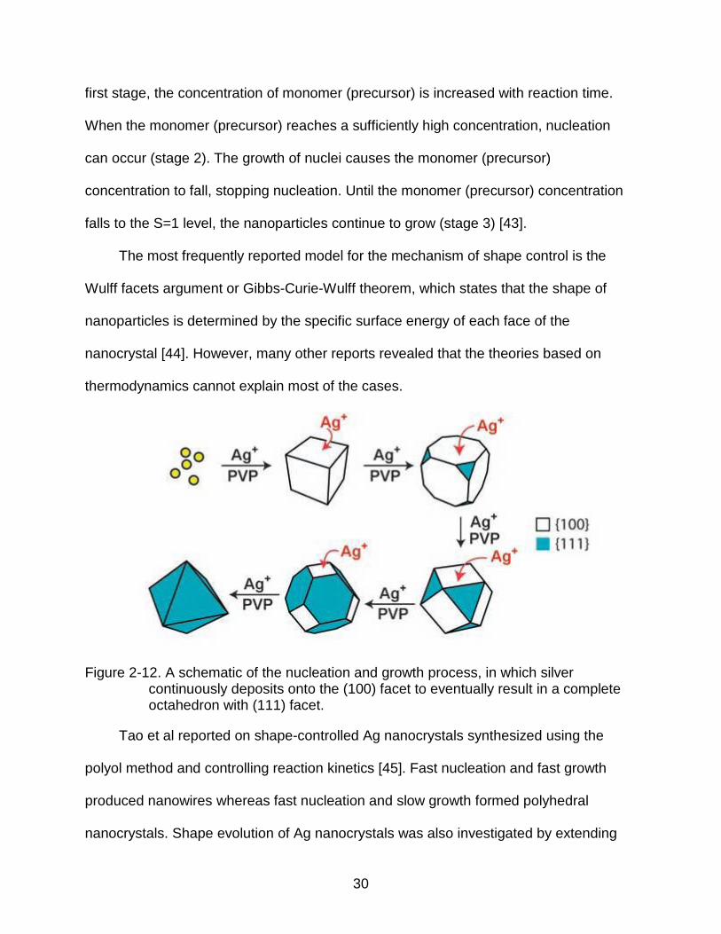
2-12 A schematic of the nucleation and growth process, in which silver continuously deposits onto the (100) facet to eventually result in a complete octahedron with (111) facet. ............................................................................... 30
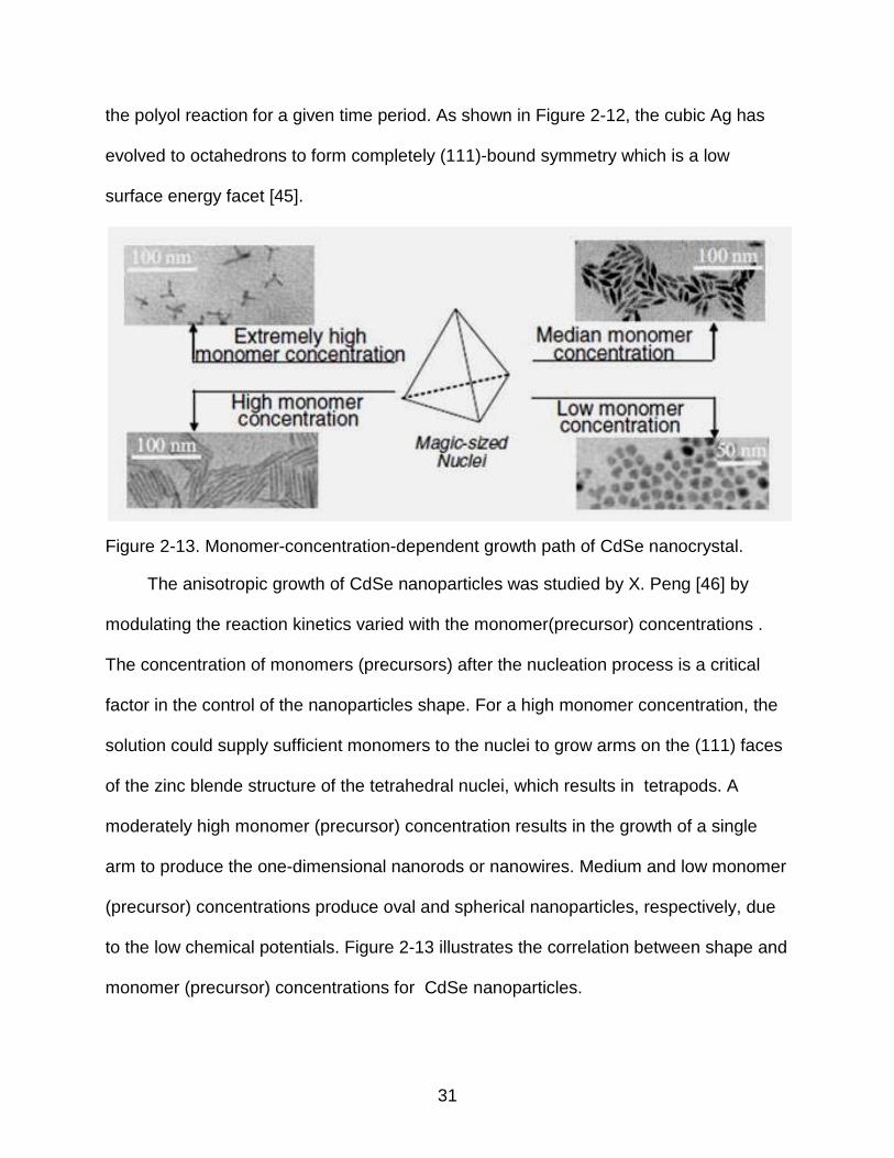
2-13 Monomer-concentration-dependent growth path of CdSe nanocrystal. .............. 31
2-14 Formation of rare-earth oxide nanopolyhedra, nanoplates, and nanodisks. ....... 32
10
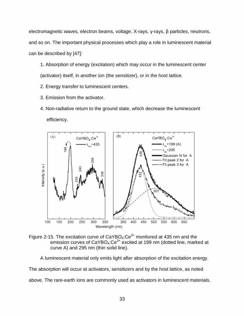
2-15 The excitation curve of CaYBO4:Ce3+ monitored at 435 nm and the emission curves of CaYBO4:Ce3+ excited at 199 nm (dotted line, marked at curve A) and 295 nm (thin solid line). ............................................................................... 33
2-16 Emission transitions in a semiconductor. The band gap Eg separates the valence band (VB) and the conduction band (CB). Excitation over the band gap creates electrons in CB and holes in VB...................................................... 35
2-17 Absorption (solid lines) and photoluminescence (dotted lines) spectra of CdS nano-rod. ............................................................................................................ 36
2-18 Color diagram of the CIE (CIE=Commission Internationale d'Eclairage) and CIE with Color Temperature Line. ...................................................................... 37
2-19 Fundamental construction of the fluorescent lamp. ............................................ 38
2-20 Scheme of relaxation of electronic excitations general scheme, and rare-earth containing scintillators. .............................................................................. 42
2-21 Schematic diagram of a scintillation detector ..................................................... 43
2-22 Schematic diagram of positron emission tomography (PET) with the inset illustrating BGO detectors coupled with PMT and a PET scan image of a brain. .................................................................................................................. 45
2-23 Pulse-height spectrum of a 137Cs source measured with a 100cm2 area and 2mm depth with LSO crystal coupled with a Hamamatsu R878 PMT. ................ 46
2-24 Schematic illustration of the density of states in metal and semiconductor clusters. .............................................................................................................. 47
2-25 Absorbance properties of II-VI semiconductor nanoparticles.............................. 48
2-26 Schematic of organic and inorganic passivation. ................................................ 49
2-27 The absorption spectra of CdSe/ZnSe nanocrystals during the shell growth. .... 50
2-28 Plot of PL intensity of the 5D0−7F2 emission at 619 nm versus the YPO4/YVO4:Eu3+ molar ratio. .............................................................................. 51
3-1 Flow chart of non-hydrolytic hot-solution synthesis procedure. .......................... 54
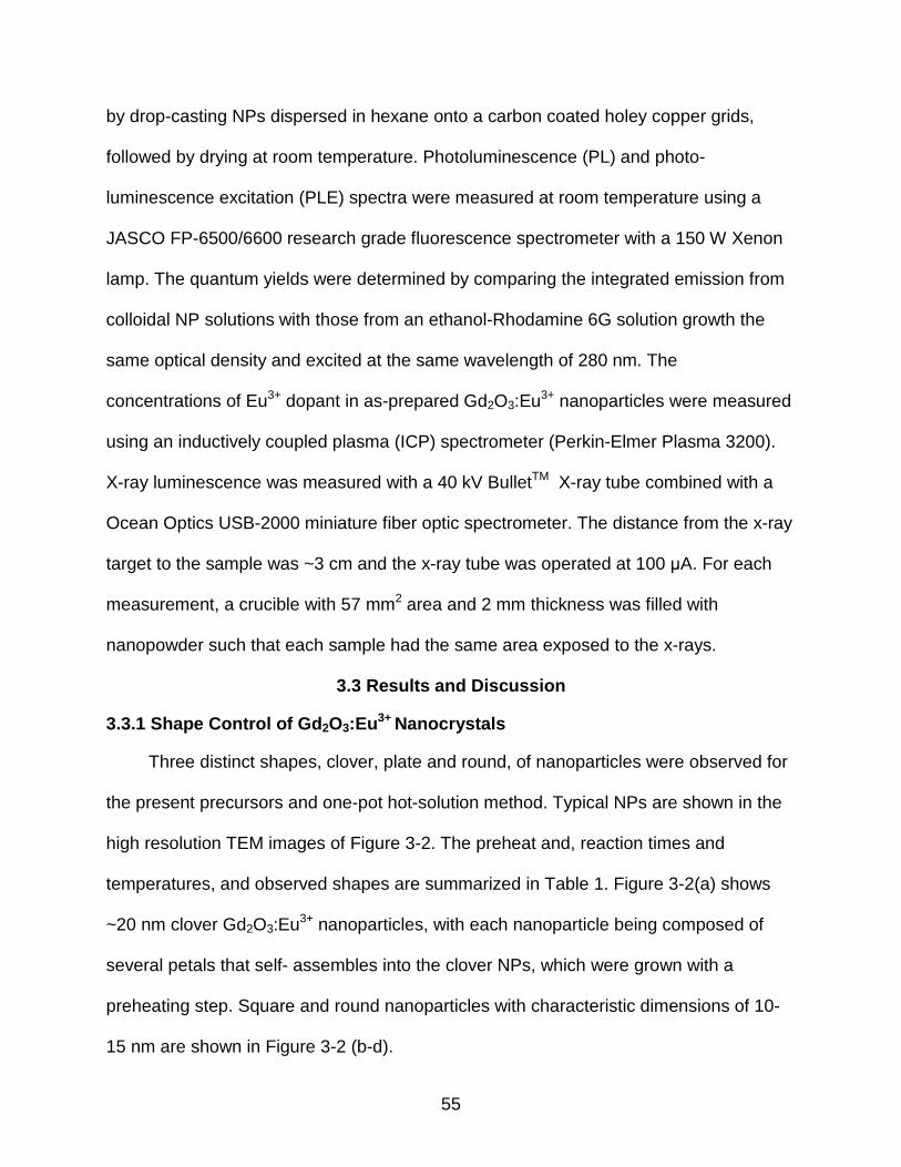
3-2 TEM images of Gd2O3:Eu3+ nanoparticles synthesized with different experimental parameters. ................................................................................... 56
3-3 Modified LaMer plots with an additional axis of reaction temperature. S=Sc: Critical saturation of monomer concentration to induce nucleation. S=1: Equilibrium monomer concentration below which growth stops.......................... 57
11
3-4 XRD patterns of as-synthesized samples. .......................................................... 58
3-5 PL and PLE spectra of Gd2O3:Eu3+ nanoparticles. The PL spectra of excitation at 250 nm and the PLE spectra for the emission at 609 nm. .............. 59
3-6 Resolved PL spectra of square nanoparticles with reaction time of 40 min (H2), round nanoparticles with reaction time for 90 min (H3) and for 180 min (H4). ................................................................................................................... 60
3-7 X-ray luminescence spectrum of as-prepared sphere-like Gd2O3:Eu3+ nanocrystals ....................................................................................................... 63
4-1 XRD patterns of calcined samples: Gd2O3:Eu3+ nanocores; Gd2O3:Eu3+/Y2O3 core/shell nanoparticles with the shell grown with a Y to Gd+Eu precursor ratio R = 1:4 and 1:1 and pure Y2O3 nanoparticles. ............................................ 68
4-2 Resolved XRD peak of Gd2O3:Eu3+/Y2O3 core/shell nanoparticles with shell grown with a Y to Gd+Eu precursor ratio R =1:1 ................................................ 69
4-3 TEM images of Gd2O3:Eu3+,Y2O3 and Gd2O3:Eu3+/Y2O3 core/shell nanoparticles: Gd2O3:Eu3+core, Gd2O3:Eu3+/Y2O3 (R=1:8), Gd2O3:Eu3+/Y2O3 (R=1:4), Gd2O3:Eu3+/Y2O3 (R=1:1), High resolution of Gd2O3:Eu3+/Y2O3 (R=1:1), and Y2O3. .............................................................................................. 70
4-4 XPS peaks from Gd2O3:Eu3+ and Gd2O3:Eu3+/Y2O3 core/shell nanoparticles grown with different precursor molar ratios (R) and normalized intensity of the Gd 3d5/2 peak versus Y2O3 shell thickness. ........................................................ 71
4-5 Idealized concentric spherical core/shell structure from which a maximum shell thickness for a given R can be calculated. ................................................. 72
4-6 PL and PLE spectra from Gd2O3:Eu3+ and Gd2O3:Eu3+/Y2O3 core/shell nanoparticles. The PLE spectra are for emission at 612 nm and the PL spectra are for excitation at 250 nm. The inset shows the uncorrected PL peak intensity versus the value of R. .................................................................. 73
4-7 Integrated area of PL peak at 612 nm versus R; Solid squares are uncorrected data. Solid diamonds are uncorrected normalized data. Open circles are normalized and corrected for the fraction of non-luminescent Y2O3 based on the value of R. ..................................................................................... 75
4-8 Luminescence decay data for the Eu3+ 5D0-7F2 transition (612 nm peak). The data are well fit by the solid line which is a single exponential function with a time constant ...................................................................................................... 77
5-1 TEM photomicrographs of dual-shell. ................................................................. 83
12
5-2 X-Ray diffraction spectra obtained from pure amorphous silica nanoparticles or calcined SiO2/Gd2O3:Eu3+ core/single-shell nanoparticles and calcined SiO2/Gd2O3:Eu3+/Y2O3 core/dual-shell nanoparticles. ......................................... 84
5-3 X-ray photoelectron peaks from the SiO2 nanocores (solid line), from SiO2/Gd2O3:Eu3+ core/single-shell (dashed line) and SiO2/Gd2O3:Eu3+/Y2O3 core/dual-shell nanoparticles (dotted line). ......................................................... 85
5-4 The Si 2p XPS peaks from SiO2, SiO2/Gd2O3:Eu3+ core/single-shell nanoparticles and normalized intensity of the Si 2p peak versus Gd2O3:Eu3+ shell thickness. ................................................................................................... 85
5-5 Photoluminescence (PL) and photoluminescence excitation (PLE) spectra from SiO2/Gd2O3:Eu3+ core/single-shell and SiO2/Gd2O3:Eu3+/Y2O3 core/dual-shell nanoparticles. The PLE spectra are for emission at 612 nm and the PL spectra are for excitation at 250 nm. .................................................................. 86
5-6 Model of a spherical core/concentric dual-shell structure from which the weight of nanoparticles necessary for a constant volume of luminescent Gd2O3:Eu3+ can be determined. .......................................................................... 87
5-7 Schematic diagram of thin film quantum yield (QY) measurement. .................... 88
5-8 Luminescence decay data for the Eu3+ 5D0 – 7F2 transition (612 nm peak). The data fit very well a single exponential decay (solid line) with a time constant τ. .......................................................................................................... 89
6-1 Flow chart of two-pot hot-solution growth of GSO nanoparticles ........................ 94
6-2 Thermogravimetric analysis (TGA) data for HSG Gd2SiO5:Ce3+ 0.5% nanoparticles. Heating rate is 10 °Cmin-1. .......................................................... 96
6-3 XRD patterns from Gd2SiO5:Ce3+ nanoparticles compared to the JCDPS pattern for monoclinic Gd2SiO5 (JCPDS # : 40-0282) : GSO:Ce3+ nanoparticles after calcination at 600 °C and 1000 °C for 2hr in air. .................. 97
6-4 TEM images of Gd2SiO5:Ce3+ nanoparticles prepared by the sol-gel (SG) method and the hot-solution (HSG) method. ...................................................... 98
6-5 PL spectra and intensity for various Ce concentrations showing quenching for Gd2SiO5:Ce3+ nanoparticles synthesized by the hot-solution method (excitation wavelength = 344 nm). ..................................................................... 99
6-6 PL and PLE spectra from Gd2SiO5:Ce3+ nanoparticles calcined at 600 °C (dashed line) and 1000 °C (solid line). .............................................................. 100
6-7 Configuration coordinate model energy levels for Ce3+ ions in a Gd2SiO5 host. ......................................................................................................................... 101

13
6-8 X-ray luminescence spectrum of calcined Gd2SiO5:Ce3+ nanoparticles. .......... 102
6-9 Differential pulse height spectrum of calcined GSO:Ce3+ nanoparticles by an 241Am source showing a broad scintillation response centered at approximately channel 300. .............................................................................. 103
8-1 SiO2/Gd2O3:Eu3+/Y2O3/SiO2 core/multi-shell nanoparticles ............................... 108
14
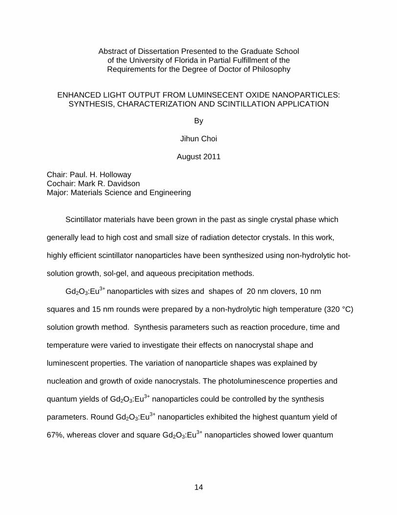
Abstract of Dissertation Presented to the Graduate School of the University of Florida in Partial Fulfillment of the Requirements for the Degree of Doctor of Philosophy
ENHANCED LIGHT OUTPUT FROM LUMINSECENT OXIDE NANOPARTICLES: SYNTHESIS, CHARACTERIZATION AND SCINTILLATION APPLICATION
By
Jihun Choi
August 2011
Chair: Paul. H. Holloway Cochair: Mark R. Davidson Major: Materials Science and Engineering
Scintillator materials have been grown in the past as single crystal phase which
generally lead to high cost and small size of radiation detector crystals. In this work,
highly efficient scintillator nanoparticles have been synthesized using non-hydrolytic hot-
solution growth, sol-gel, and aqueous precipitation methods.
Gd2O3:Eu3+ nanoparticles with sizes and shapes of 20 nm clovers, 10 nm
squares and 15 nm rounds were prepared by a non-hydrolytic high temperature (320 °C)
solution growth method. Synthesis parameters such as reaction procedure, time and
temperature were varied to investigate their effects on nanocrystal shape and
luminescent properties. The variation of nanoparticle shapes was explained by
nucleation and growth of oxide nanocrystals. The photoluminescence properties and
quantum yields of Gd2O3:Eu3+ nanoparticles could be controlled by the synthesis
parameters. Round Gd2O3:Eu3+ nanoparticles exhibited the highest quantum yield of
67%, whereas clover and square Gd2O3:Eu3+ nanoparticles showed lower quantum
15
yields of 24% and 48%, respectively. The luminescent properties were discussed in
terms of doping concentration, host environment and dopant location.
Nanoparticles of Gd2O3:Eu3+ ~20 nm in diameter were synthesized at ~180° C
using a facile high boiling-point alcohol (polyol) method. The Gd2O3 nanoparticles,
doped with 5 mol% Eu, were crystalline cubic phase and exhibited intense 5D0-7F2
photoluminescence (PL) from Eu3+ after calcination at 600 ˚C for 2h in air.
Photoluminescence excitation (PLE) data showed that while a small fraction of the
emission resulted from direct excitation of Eu3+, most of the excitation resulted from
adsorption in the Oxygen to Europium charge-transfer band between 225 and 275 nm.
Transmission electron microscopy (TEM) images showed that the Gd2O3:Eu3+ cores
were slightly agglomerated, but the thin Y2O3 shell could not be detected by TEM. X-ray
photoelectron spectroscopy (XPS) was used to detect the thin Y2O3 shell around the
Gd2O3:Eu3+ core. Drop-cast thin films of the Gd2O3:Eu3+/Y2O3 core/shell nanoparticles
exhibited PL intensities up to 40% larger than from bare core Gd2O3:Eu3+ nanoparticles.
Increased PL was attributed to reduced non-radiative recombination based on longer
luminescence decay times.
Spherical SiO2 cores have been coated with oxide dual-shells of Gd2O3:Eu3+ and
Y2O3 by a solution precipitation method. Based on transmission electron microscopy
(TEM) data, luminescent Gd2O3:Eu3+ shells with ~4.5 nm thickness were successfully
coated on mono-dispersed SiO2 nanocores ~210 ± 15 nm in radius. A continuous Y2O3
shell ∼45 nm thick was then grown on the SiO2/Gd2O3:Eu3+ nanoparticles. The
SiO2/Gd2O3:Eu3+ core/shell nanoparticles exhibited 5D0-7F2 photoluminescence (PL)
from Eu3+ transitions after calcination at 600°C for 2h in air. Photoluminescence
16
excitation (PLE) data showed that most of the excitation resulted from absorption in the
oxygen to europium charge-transfer band between 225 and 275 nm. Drop-cast thin
films of core/dual-shell samples exhibited quantum yields (QYs) up to 2 times larger
than that of core/single-shell nanoparticles, which was attributed to reduced non-
radiative recombination, consistent with longer luminescence decay lifetimes.
Nanophosphor Gd2SiO5:Ce3+ (GSO) with sizes between 2 nm - 5 nm was
synthesized by sol-gel and hot-solution methods. X-Ray luminescence,
photoluminescence (PL) and structural properties of GSO:Ce3+ nanoparticles were
compared for the two different synthesis methods. PL and X-ray luminescence were
both from the Ce3+ 5d-4f transitions at 390~430 °C. The Ce dopant concentration was
varied between 0.1% - 10% and concentration quenching was observed at 0.5% under
UV excitation. Hot-solution synthesized GSO doped with ≤0.5% Ce exhibited PL after
calcination at either 600 ˚C or 1000 ˚C for 2 h in air, while GSO:Ce3+ nanoparticles
prepared by the sol-gel method required calcination at 1000 ˚C to observe PL.
17
CHAPTER 1 INTRODUCTION
“Nano” is one of the most frequently cited words in recent science and engineering
fields. Micro and nano fabrication is a representative approach of “top-down” application
of the nano-world, which has been led by the Si based electronic devices. The typical
example of “bottom-up” technology in the nano-world is a synthesis of nanoparticles,
often used as nanocrystals and nanoclusters. Nanoparticles mean nanometer scale
particles that are neither small molecules nor bulk solids. In the nanometer scale regime,
the physical and chemical properties of materials become unique and novel compared
to their bulk counterpart. Among various characteristics of nanoparticles, luminescent
properties will be the main focus of my dissertation.
The aim of the work described in this dissertation is to synthesize highly
luminescent oxide nanoparticles for scintillation (i.e. luminescence due to energetic
particle radiation). To achieve this goal, the following approach was used
1. Synthesize cores and/or core/shell luminescent oxide nanoparticles using
solution based synthesis methods.
2. Characterize the structure, morphology, surface, photoluminescence and X-ray
luminescence of the oxide nanoparticles.
3. Evaluate the mechanisms to enhance the light output from luminescent oxide
nanoparticles.
In the dissertation, Chapter 2 reviews the fundamentals of nanoparticles, their
various synthesis methods and applications in different fields. The fundamentals of
luminescent materials and several approaches to achieve enhanced luminescence are
also reviewed. In Chapter 3, the preparation of shape-controlled gadolinium oxide
18
doped with europium nanoparticles with a non-hydrolytic synthesis is discussed. The
mechanism of nucleation and growth of oxide nanoparticles were also reviewed. In
Chapter 4, the synthesis and characterization of gadolinium oxide nanocores doped
with europium/yttrium oxide core/shell hetero structures is discussed. Luminescent
cores could be passivated by a non-luminescent shell with a facile polyol synthesis
method so that enhanced photoluminescence was achieved. In Chapter 5, silica
core/dual-shell structures are created and characterized. Silica cores have several
advantages such as uniformly spherical shape, ease of synthesis and low cost.
Luminescent shell with europium doped gadolinium oxide was grown on silica
nanocores. In addition, core/single-shell structures could be coated by yttrium oxide
outer shell to passivate non-radiative defects by solution precipitation method. The
passivation of surface defects was postulated based on a longer luminescent decay
lifetime. Chapter 6 describes the synthesis and characterization of gadolinium silicate
(GSO) nanoparticles doped with cerium ions. Single crystals of GSO are used in a
scintillation detector. GSO nanoparticles were synthesized by both hot-solution and sol-
gel method and their properties were compared. Finally, Conclusions and Future Work
are summarized in Chapter 7 and 8.

19
CHAPTER 2 LITERATURE REVIEW
2.1 Fundamental of Colloidal Nanoparticles
The development of small size materials is of interests for chemical and material
research. The electronic industry with semiconductor devices is a good example of the
approach of novel materials, where the size of devices has steadily decreased to the
nanometer dimension for the reduction of power consumption and increased computing
speed. The counterpart of a micro-fabrication is synthesis of nanoparticles. The
synthesis and application of nanoparticles have been intensively studied to understand
fundamental phenomena and scientific properties. Nanoparticles exhibit novel
properties and functions due to their small size, typically under 100 nm.
2.1.1 Synthesis Process for Colloidal Nanoparticles
Nanoparticles can be synthesized using at least two different general methods,
i.e. “top-down” and “bottom-up” approaches. A top-down method uses physical methods
such as milling and micro-fabrication, while a bottom-up method utilizes liquid phase
colloidal chemistry. In our study, the bottom-up methods will be used to synthesize
nanoparticles due to their advantages in controlling size and shape. Several ‘bottom-up’
synthesis methods will be introduced.
Many of the earliest synthesis of nanoparticles were synthesized by the
precipitation method from aqueous solutions followed by thermal decomposition of
precursors. For example, Cu, Ag, Pt, Ni, Co and Au nanoparticles were achieved by the
precipitation method [1-5]. The precipitation of metals from aqueous or non-aqueous
solutions typically requires the reduction of metal cations. Oxide nanoparticles also
could be synthesized by the precipitation method. The precipitation of oxide
20
nanoparticles, from both aqueous and non-aqueous solutions can be broken into two
categories, i.e. those that produce modified precursors which must undergo further
processing such as calcinations, and those that produce oxide nanoparticles directly.
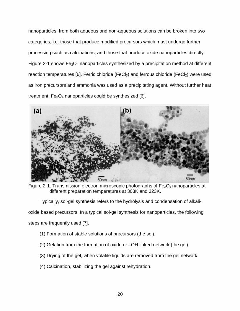
Figure 2-1 shows Fe3O4 nanoparticles synthesized by a precipitation method at different
reaction temperatures [6]. Ferric chloride (FeCl3) and ferrous chloride (FeCl2) were used
as iron precursors and ammonia was used as a precipitating agent. Without further heat
treatment, Fe3O4 nanoparticles could be synthesized [6].
Figure 2-1. Transmission electron microscopic photographs of Fe3O4 nanoparticles at different preparation temperatures at 303K and 323K.
Typically, sol-gel synthesis refers to the hydrolysis and condensation of alkali-
oxide based precursors. In a typical sol-gel synthesis for nanoparticles, the following
steps are frequently used [7].
(1) Formation of stable solutions of precursors (the sol).
(2) Gelation from the formation of oxide or –OH linked network (the gel).
(3) Drying of the gel, when volatile liquids are removed from the gel network.
(4) Calcination, stabilizing the gel against rehydration.
21
It is reported that oxide nanoparticles have been synthesized by a sol-gel method.
Titania nanoparticles were easily prepared by controlled hydrolysis and condensation of
Ti(OiPr)- (titanium isopropoxide) in an alcohol solution acidified by HCl after drying [8, 9].
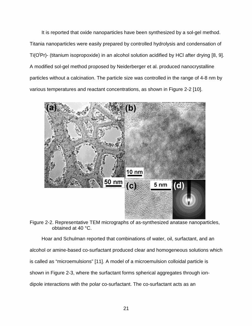
A modified sol-gel method proposed by Neiderberger et al. produced nanocrystalline
particles without a calcination. The particle size was controlled in the range of 4-8 nm by
various temperatures and reactant concentrations, as shown in Figure 2-2 [10].
Figure 2-2. Representative TEM micrographs of as-synthesized anatase nanoparticles, obtained at 40 °C.
Hoar and Schulman reported that combinations of water, oil, surfactant, and an
alcohol or amine-based co-surfactant produced clear and homogeneous solutions which
is called as “microemulsions” [11]. A model of a microemulsion colloidal particle is
shown in Figure 2-3, where the surfactant forms spherical aggregates through ion-
dipole interactions with the polar co-surfactant. The co-surfactant acts as an
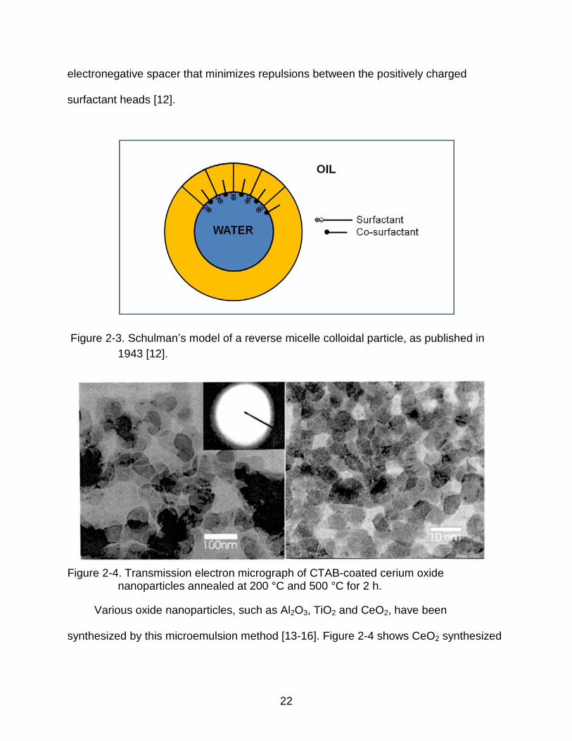
22
electronegative spacer that minimizes repulsions between the positively charged
surfactant heads [12].
Figure 2-3. Schulman’s model of a reverse micelle colloidal particle, as published in 1943 [12].
Figure 2-4. Transmission electron micrograph of CTAB-coated cerium oxide nanoparticles annealed at 200 °C and 500 °C for 2 h.
Various oxide nanoparticles, such as Al2O3, TiO2 and CeO2, have been
synthesized by this microemulsion method [13-16]. Figure 2-4 shows CeO2 synthesized
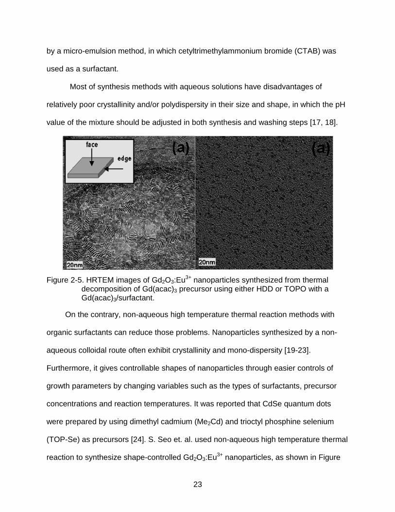
23
by a micro-emulsion method, in which cetyltrimethylammonium bromide (CTAB) was
used as a surfactant.
Most of synthesis methods with aqueous solutions have disadvantages of
relatively poor crystallinity and/or polydispersity in their size and shape, in which the pH
value of the mixture should be adjusted in both synthesis and washing steps [17, 18].
Figure 2-5. HRTEM images of Gd2O3:Eu3+ nanoparticles synthesized from thermal decomposition of Gd(acac)3 precursor using either HDD or TOPO with a Gd(acac)3/surfactant.
On the contrary, non-aqueous high temperature thermal reaction methods with
organic surfactants can reduce those problems. Nanoparticles synthesized by a non-
aqueous colloidal route often exhibit crystallinity and mono-dispersity [19-23].
Furthermore, it gives controllable shapes of nanoparticles through easier controls of
growth parameters by changing variables such as the types of surfactants, precursor
concentrations and reaction temperatures. It was reported that CdSe quantum dots
were prepared by using dimethyl cadmium (Me2Cd) and trioctyl phosphine selenium
(TOP-Se) as precursors [24]. S. Seo et. al. used non-aqueous high temperature thermal
reaction to synthesize shape-controlled Gd2O3:Eu3+ nanoparticles, as shown in Figure

24
2-5, where the dimensions of nano-plates was an edge length and a thickness of 5 nm
and 1 nm, respectively [25].
2.1.2 Shape Control of Colloidal Nanoparticles
2.1.2.1 Shapes of nanoparticles
Figure 2-6. Change in bandgap energy, ΔEg, versus d (thickness or diameter) or length/diameter ratio [26].
It is well known that quantum effects become increasingly important as the size of
structures is reduced, but the influence of shape on quantum confinement has been
less studied. Buhro and Colvin proposed that shape matters as much as size for
nanoparticles [27]. They cited experimental work by Kan et al. which showed that the
electronic structure and optical properties of rod-like semiconductor nanocrystals
depended sensitively on the ratio of their length and diameter, as illustrated in Figure 2-
6 [26]. W.H. Qi and M.P. Wang [28] modeled the effects of shape and size on the
lattice parameters of a metallic nanoparticle formed from an ideal bulk crystal. In order
to predict shape effects on lattice parameters, they introduced a shape factor. Their
data show that the lattice parameter strongly depends on nanoparticle size and shape,
as illustrated by Figure 2-7.
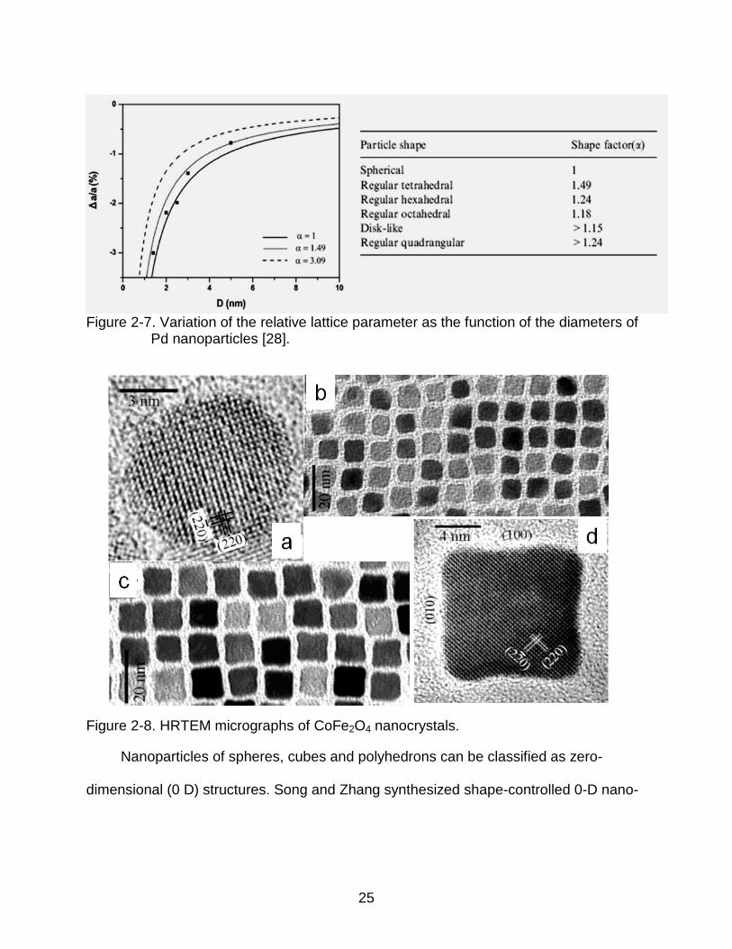
25
Figure 2-7. Variation of the relative lattice parameter as the function of the diameters of Pd nanoparticles [28].
Figure 2-8. HRTEM micrographs of CoFe2O4 nanocrystals.
Nanoparticles of spheres, cubes and polyhedrons can be classified as zero-
dimensional (0 D) structures. Song and Zhang synthesized shape-controlled 0-D nano-
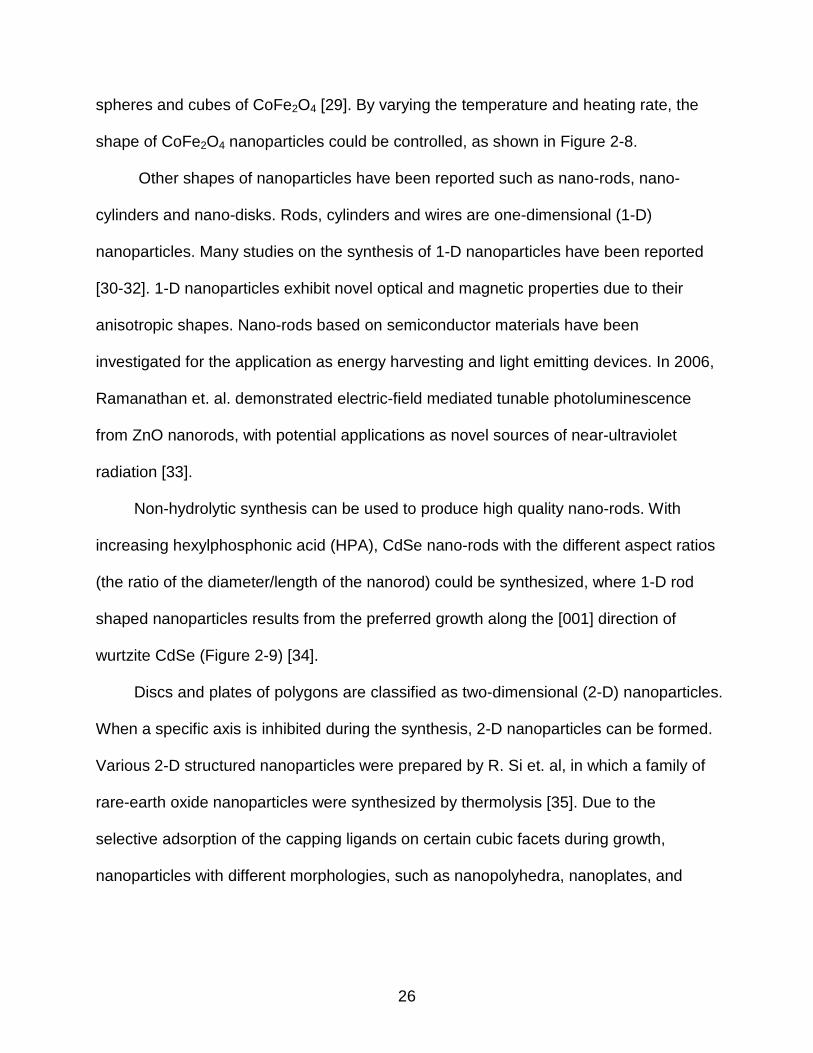
26
spheres and cubes of CoFe2O4 [29]. By varying the temperature and heating rate, the
shape of CoFe2O4 nanoparticles could be controlled, as shown in Figure 2-8.
Other shapes of nanoparticles have been reported such as nano-rods, nano-
cylinders and nano-disks. Rods, cylinders and wires are one-dimensional (1-D)
nanoparticles. Many studies on the synthesis of 1-D nanoparticles have been reported
[30-32]. 1-D nanoparticles exhibit novel optical and magnetic properties due to their
anisotropic shapes. Nano-rods based on semiconductor materials have been
investigated for the application as energy harvesting and light emitting devices. In 2006,
Ramanathan et. al. demonstrated electric-field mediated tunable photoluminescence
from ZnO nanorods, with potential applications as novel sources of near-ultraviolet
radiation [33].
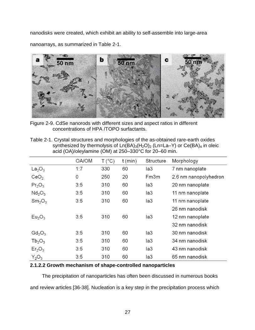
Non-hydrolytic synthesis can be used to produce high quality nano-rods. With
increasing hexylphosphonic acid (HPA), CdSe nano-rods with the different aspect ratios
(the ratio of the diameter/length of the nanorod) could be synthesized, where 1-D rod
shaped nanoparticles results from the preferred growth along the [001] direction of
wurtzite CdSe (Figure 2-9) [34].
Discs and plates of polygons are classified as two-dimensional (2-D) nanoparticles.
When a specific axis is inhibited during the synthesis, 2-D nanoparticles can be formed.
Various 2-D structured nanoparticles were prepared by R. Si et. al, in which a family of
rare-earth oxide nanoparticles were synthesized by thermolysis [35]. Due to the
selective adsorption of the capping ligands on certain cubic facets during growth,
nanoparticles with different morphologies, such as nanopolyhedra, nanoplates, and
27
nanodisks were created, which exhibit an ability to self-assemble into large-area
nanoarrays, as summarized in Table 2-1.
Figure 2-9. CdSe nanorods with different sizes and aspect ratios in different concentrations of HPA /TOPO surfactants.
Table 2-1. Crystal structures and morphologies of the as-obtained rare-earth oxides synthesized by thermolysis of Ln(BA)3(H2O)2 (Ln=La–Y) or Ce(BA)4 in oleic acid (OA)/oleylamine (OM) at 250–330°C for 20–60 min.
2.1.2.2 Growth mechanism of shape-controlled nanoparticles
The precipitation of nanoparticles has often been discussed in numerous books
and review articles [36-38]. Nucleation is a key step in the precipitation process which
28
can be explained by thermodynamics. Assuming that some of atoms of the liquid cluster
together to form a small sphere of solid, the free energy of the systems can be express
by [39]:
G1 = (VS + VL)GVL (2-1)
G2 = VSGVS + VLGVL + ASLγSL (2-2)
Where G1 and G2 are free energy of two systems, VS is the volume of the solid
sphere, VL the volume of liquid, ASL is the solid/liquid interfacial area, GVS and GV
L are
the free energies per unit volume of solid and liquid respectively, and γSL the solid/liquid
interfacial free energy. The change of free energy (ΔGV) from G1 to G2,with a sphere of
radius r, is given by Equation 2-3 as
∆Gr = −43πr3∆GV + 4πr2γSL (2-3)
It can be seen from Figure 2-10 that for a given undercooling, cooling a material
below the transformation temperature without obtaining the transformation, there is a
certain radius, r*, which is associated with a maximum excess free energy. When r > r*,
the free energy of the system decreases if the solid either grows or shrinks. The critical
radius of the solid nuclei can be expressed by:
r∗ = 2γSL∆GV
= 2γSLTm∆HS
1∆T
(2-4)
where H is the enthalpy of fusion and ΔT is the degree of undercooling.
The initial stage of the growth of nuclei can be explained by heterogeneous nucleation
limited by either diffusion or reaction rates. For diffusion-limited growth, concentration
gradients and temperature control the growth rate. Ostwald ripening is a secondary
growth process in which smaller particles are consumed by larger particles [40, 41]. The

29
size, morphology and properties of nanoparticles are dramatically affected by the
Ostwald ripening.
Figure 2-10. Homogeneous nucleation and the free energy change associated with homogeneous nucleation of a sphere of radius r.
Figure 2-11. Lamer plot with illustration of nucleation and growth diagram. S=Sc: critical saturation of monomer concentration to induce nucleation. S=1: equilibrium monomer concentration below which growth stops.
A Lamer plot is used to describe the formation of clusters and colloids in
homogeneous and supersaturated solutions[42, 43]. As illustrated in Figure 2-11, in the
30
first stage, the concentration of monomer (precursor) is increased with reaction time.
When the monomer (precursor) reaches a sufficiently high concentration, nucleation
can occur (stage 2). The growth of nuclei causes the monomer (precursor)
concentration to fall, stopping nucleation. Until the monomer (precursor) concentration
falls to the S=1 level, the nanoparticles continue to grow (stage 3) [43].
The most frequently reported model for the mechanism of shape control is the
Wulff facets argument or Gibbs-Curie-Wulff theorem, which states that the shape of
nanoparticles is determined by the specific surface energy of each face of the
nanocrystal [44]. However, many other reports revealed that the theories based on
thermodynamics cannot explain most of the cases.
Figure 2-12. A schematic of the nucleation and growth process, in which silver continuously deposits onto the (100) facet to eventually result in a complete octahedron with (111) facet.
Tao et al reported on shape-controlled Ag nanocrystals synthesized using the
polyol method and controlling reaction kinetics [45]. Fast nucleation and fast growth
produced nanowires whereas fast nucleation and slow growth formed polyhedral
nanocrystals. Shape evolution of Ag nanocrystals was also investigated by extending
31
the polyol reaction for a given time period. As shown in Figure 2-12, the cubic Ag has
evolved to octahedrons to form completely (111)-bound symmetry which is a low
surface energy facet [45].
Figure 2-13. Monomer-concentration-dependent growth path of CdSe nanocrystal.
The anisotropic growth of CdSe nanoparticles was studied by X. Peng [46] by
modulating the reaction kinetics varied with the monomer(precursor) concentrations .
The concentration of monomers (precursors) after the nucleation process is a critical
factor in the control of the nanoparticles shape. For a high monomer concentration, the
solution could supply sufficient monomers to the nuclei to grow arms on the (111) faces
of the zinc blende structure of the tetrahedral nuclei, which results in tetrapods. A
moderately high monomer (precursor) concentration results in the growth of a single
arm to produce the one-dimensional nanorods or nanowires. Medium and low monomer
(precursor) concentrations produce oval and spherical nanoparticles, respectively, due
to the low chemical potentials. Figure 2-13 illustrates the correlation between shape and
monomer (precursor) concentrations for CdSe nanoparticles.
32
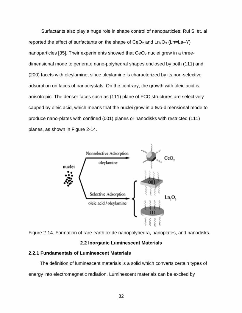
Surfactants also play a huge role in shape control of nanoparticles. Rui Si et. al
reported the effect of surfactants on the shape of CeO2 and Ln2O3 (Ln=La–Y)
nanoparticles [35]. Their experiments showed that CeO2 nuclei grew in a three-
dimensional mode to generate nano-polyhedral shapes enclosed by both (111) and
(200) facets with oleylamine, since oleylamine is characterized by its non-selective
adsorption on faces of nanocrystals. On the contrary, the growth with oleic acid is
anisotropic. The denser faces such as (111) plane of FCC structures are selectively
capped by oleic acid, which means that the nuclei grow in a two-dimensional mode to
produce nano-plates with confined (001) planes or nanodisks with restricted (111)
planes, as shown in Figure 2-14.
Figure 2-14. Formation of rare-earth oxide nanopolyhedra, nanoplates, and nanodisks.
2.2 Inorganic Luminescent Materials
2.2.1 Fundamentals of Luminescent Materials
The definition of luminescent materials is a solid which converts certain types of
energy into electromagnetic radiation. Luminescent materials can be excited by
33
electromagnetic waves, electron beams, voltage, X-rays, γ-rays, β particles, neutrons,
and so on. The important physical processes which play a role in luminescent material
can be described by [47]:
1. Absorption of energy (excitation) which may occur in the luminescent center
(activator) itself, in another ion (the sensitizer), or in the host lattice.
2. Energy transfer to luminescent centers.
3. Emission from the activator.
4. Non-radiative return to the ground state, which decrease the luminescent
efficiency.
Figure 2-15. The excitation curve of CaYBO4:Ce3+ monitored at 435 nm and the emission curves of CaYBO4:Ce3+ excited at 199 nm (dotted line, marked at curve A) and 295 nm (thin solid line).
A luminescent material only emits light after absorption of the excitation energy.
The absorption will occur at activators, sensitizers and by the host lattice, as noted
above. The rare-earth ions are commonly used as activators in luminescent materials.
34
They are characterized by an incompletely filled 4f shell. For example, Eu3+, Yb3+, Er3+
and Nb3+ ions show charge-transfer absorption bands and Ce3+, Pr3+, Tb3+ show 4f →
5d absorption bands in the ultraviolet [47]. A typical photoluminescence excitation (PLE)
spectrum from Ce3+ doped CaYBO4 is shown in Figure 2-15 [48]. The absorption of
energy does not necessarily take place at the activator, but may also occur in the host
lattice. There are two different classes of optical absorption transitions. One results in
free electrons and holes and another does not make free charge carriers [47]. ZnS is an
example of the former class. It is a compound semiconductor. Optical absorption occurs
for energies larger than the width of the band gap (Eg) and it creates electrons in the
conduction band and holes in the valence band. However, not every host lattice makes
free charge carriers by optical excitation. For example, in CaWO4, energy is absorbed in
the WO42- complex. In the excited state of the tungsten group, the hole and the electron
form an exciton.
Once luminescent materials absorb enough energy to make excited carriers or
excitons (electron-hole pair), light is emitted by relaxation of excited carriers to lower
energy state, and ultimately to the ground state. In terms of the emission from activators,
rare-earth ions could be used for a typical example. The emission of Eu3+ ions consists
usually of peaks with a small FWHM because they show parallel parabolas (ΔR = 0) in a
configurational coordinate diagram [47]. The line emissions corresponds to transitions
from the excited 5D0 to the 7FJ (J = 0, 1, 2, 3, 4, 5, 6) levels of the 4f6 configuration [49].
The transition 5D0 → 7F2,4 of Eu3+ is a forbidden electric-dipole transition (parity selection
rule), whereas the 5D0 → 7F1,3 of Eu3+ is an allowed magnetic-dipole transition [47].
35
However, this selection rule can be relaxed for Eu3+ in a host lattice lacking inversion
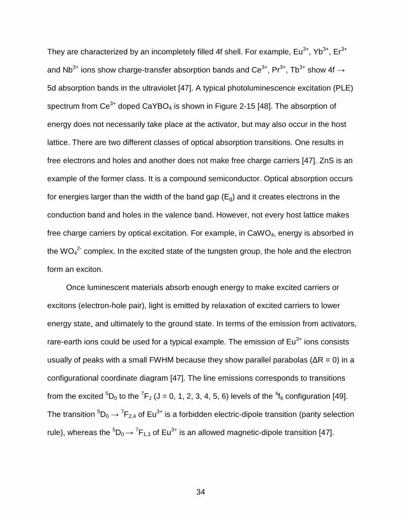
symmetry, such as Gd2O3, Y2O3 and LaPO4 [50-52].
Figure 2-16. Emission transitions in a semiconductor. The band gap Eg separates the valence band (VB) and the conduction band (CB). Excitation over the band gap creates electrons in CB and holes in VB.
In semiconductors, there are several paths to explain a radiative process. As
illustrated in Figure 2-16, emission from a semiconductor can be achieved by [47]:
(1) recombination of free electrons and holes
(2) a free hole recombines with an electron trapped in a shallow trap level
(3) the same with a deep electron-trapping level
(4) a free electron recombines with a trapped hole
(5) doner-acceptor pair emission
(vi) electron-hole recombination at a donor-acceptor complex
(e.g. at coupled defects such as vacancy and substitution of atoms)
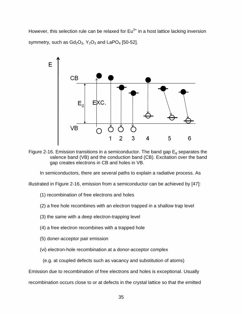
Emission due to recombination of free electrons and holes is exceptional. Usually
recombination occurs close to or at defects in the crystal lattice so that the emitted
36
wavelength should be increased (lower energy). This energy shift is called the Stokes
shift and is shown for a CdS nanorods in Figure 2-17 [53].
Figure 2-17. Absorption (solid lines) and photoluminescence (dotted lines) spectra of CdS nano-rod.
2.2.2 Application of Luminescent Materials
The application of luminescent materials can be classified by the excitation
sources for the luminescent materials as shown in Table 2-2 [54]. Luminescent
materials can be found in a broad range of everyday applications such as cathode ray
tubes (CRTs), projection televisions, fluorescent lamps, X-ray detectors, solid state
lighting, sensors, and displays. Generally, research and development on luminescent
materials has resulted in synthesis and testing of thousands of phosphors [54]. However,
only about 50 materials exhibit properties that are suitable for appropriate technological
applications in terms of efficiency, emission color, decay time, physical stability,
availability of raw materials, environmental aspects, cost, reproducibility and ease of
materials preparation [55-57].
37
Table 2-2. Applications of luminescent materials classified by different excitation sources.
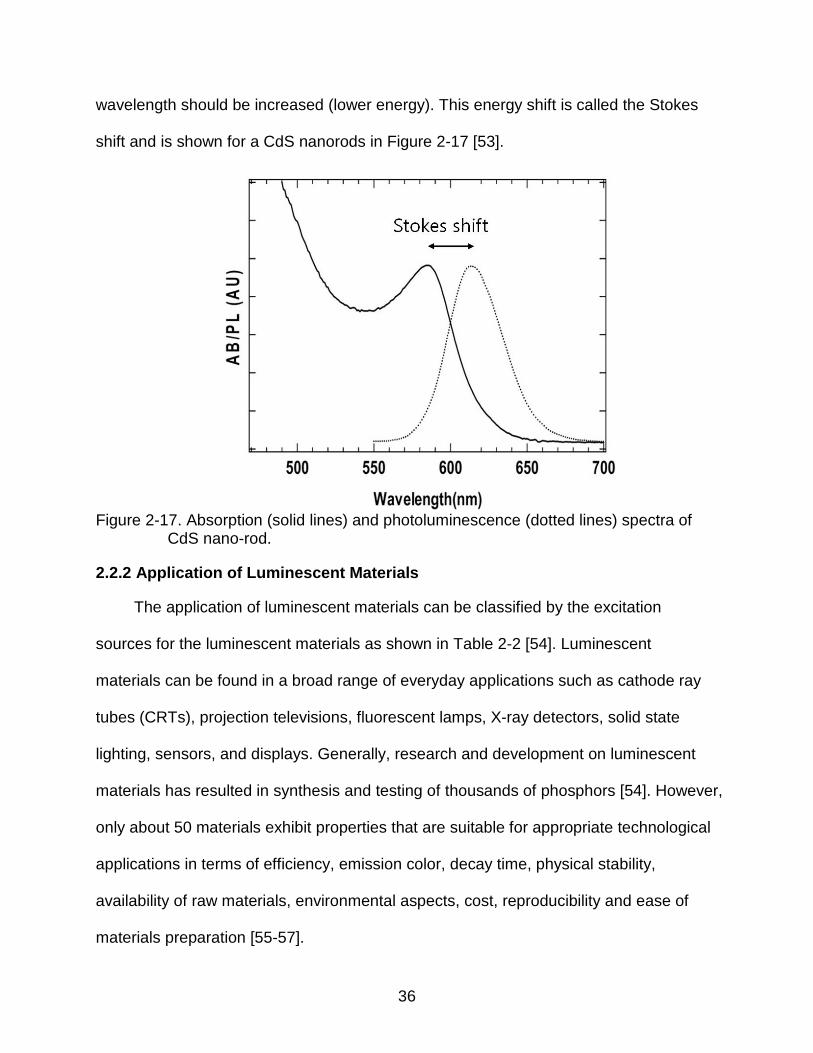
Figure 2-18. Color diagram of the CIE (CIE=Commission Internationale d'Eclairage) and CIE with Color Temperature Line.
Recently, an important application of luminescent material is to create white light
emitting diodes (LEDs). White light can be generated by combining the output from blue,
green and red-emitting diodes to yield white light. There are three different technical
approaches to realize inorganic white LEDs [58]. The first successful device combined a
blue LED covered with a classical yellow phosphor, such as yttrium aluminum garnet
Y3Al5O12 doped with Ce3+ (YAG:Ce3+) [59]. These LEDs have been widely used as
simple long-life white-light sources in traffic lights, cycle lamps, car headlights, outdoor
38
lighting or flashlights. The white light looks ‘cold’ due to its high color temperature
(CCT=>5000K). More specific applications like indoor lighting require warm-white light
and an excellent color rendering. The white light should contain red wavelength regions
and thus exhibit a lower color temperature. These targets are achieved by a
combination of a blue (Ga,In)N LED with two phosphors emitting red and green light
[60].
In the third approach suitable phosphors for (Ga,Al)N UV LEDs are developed.
These are covered with three different phosphors, which emit red, green, and blue. The
advantage of these white LEDs is that they enable variation of three broad-band
emitters, giving access to a larger color area in the CIE diagram (Figure 2-18) and
better color rendering [61].
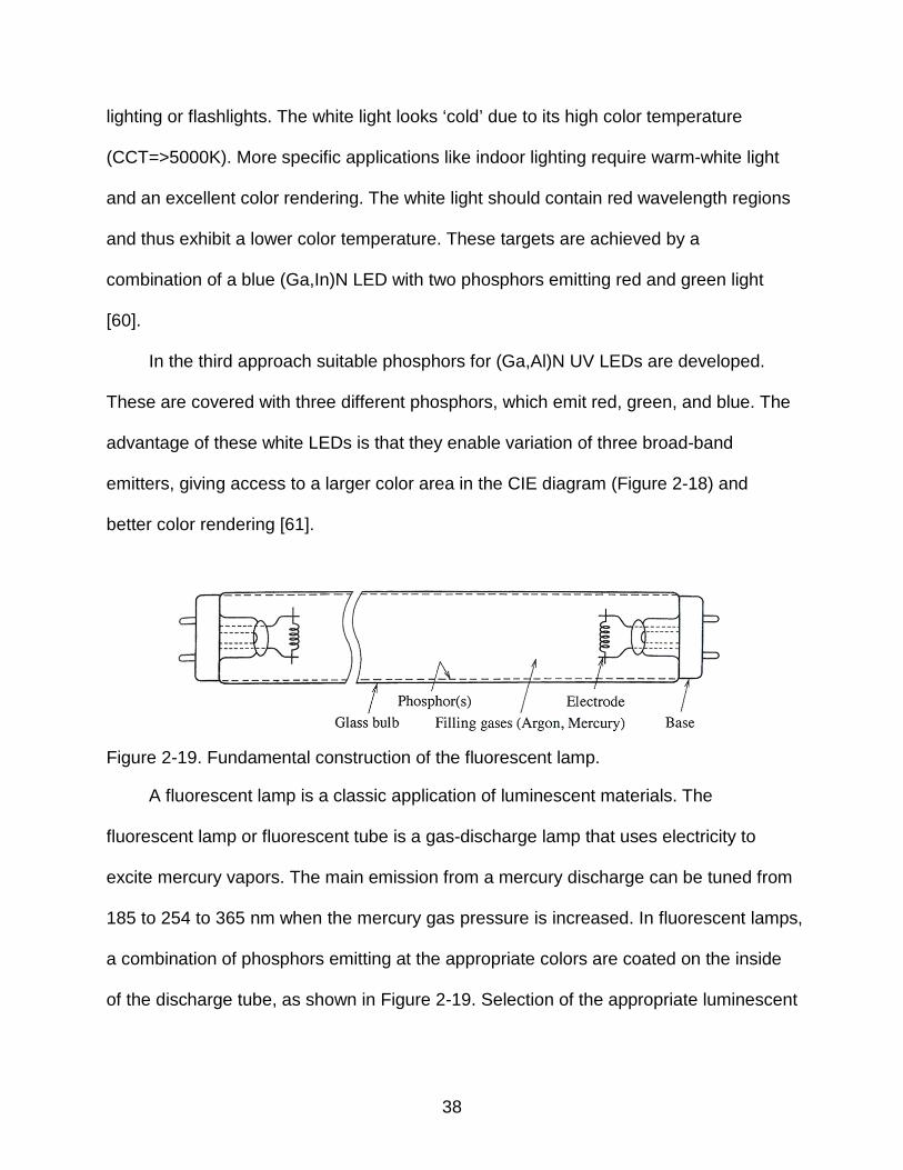
Figure 2-19. Fundamental construction of the fluorescent lamp.
A fluorescent lamp is a classic application of luminescent materials. The
fluorescent lamp or fluorescent tube is a gas-discharge lamp that uses electricity to
excite mercury vapors. The main emission from a mercury discharge can be tuned from
185 to 254 to 365 nm when the mercury gas pressure is increased. In fluorescent lamps,
a combination of phosphors emitting at the appropriate colors are coated on the inside
of the discharge tube, as shown in Figure 2-19. Selection of the appropriate luminescent
39
materials enables special application of fluorescent lamps such as security marking,
sun-tanning, photocopying, display backlight and advertising billboards [62].
2.3 Scintillation Materials
An important application of luminescent nanoparticles is a scintillator. Scintillators
are substances that absorb high energy electromagnetic or charged particle radiation
then, in response, emit photons at a desirable wavelength, releasing the previously
absorbed energy. Scintillators are used in several physics research and military
applications to detect electromagnetic waves or particles. Scintillators are usually made
of bulk single crystalline materials, which are very expensive and hard to make. Key
factors for good scintillator materials are [63].
High atomic number and density (Improve photo-absorption)
Short decay time (Improve time resolution)
High efficiency of emitting UV or visible light (Large light output)
Low afterglow
Low cost - Bulk is very expensive
Scintillator materials are characterized by high stopping power, which makes them
well-suited for detecting high-energy radiation so that high atomic number materials
have to be used. Shorter decay time results in higher count rates and time resolution.
Afterglow is the phenomenon that luminescence can still be observed a long time after
the end of the excitation pulse. A long time here is defined as a time much longer (≥ 5X)
than the decay time of the luminescence. So, for the improvement of detection, low
afterglow is a necessary behavior of good scintillator materials.
40
2.3.1 Fundamentals of Scintillation Materials
The mechanisms of excitation of the luminescent centers (activators) in a
scintillator are strongly influenced by the surrounding medium. The coupling between
the lattice and activators is essential in the way the energy is transferred between them.
Electrons and holes created by absorption of high energy radiation have several
possible pathways for the scintillation process [64]:
(1) electron + hole → h𝜈
(2) electron + hole → ex → h𝜈
(3) electron + hole + A → ex + A → A * → A + h𝜈
(4) electron + hole + A → A1+ + e → A * → A + h𝜈
(5) electron + hole + A → (A1-)* + hole → A + h𝜈
(6) A → A * → A + h𝜈
where A means activator ions and A* represents their excited states.
The simplest scintillation process (1) is the result of the direct radiative recombination of
free electrons in the conduction band with holes in the valence band. In most cases, the
recombination takes place when the energy of electrons and holes decreases because
they form bonding states called excitons (ex) with energy smaller than the bandgap.
The excited carriers can also be bound in the lattice, for example, in the vicinity of a
specific structural defect (2). They are called auto-localized excitons and their radius
depends on the electrostatic field in the configuration. Luminescence from free or bound
excitons has been observed so far only in simple oxides [65].
Sometimes, in the presence of impurity centers or activator ions (A), the exciton
luminescence is efficiently quenched, causing a sensitization of the luminescence of the

41
activating ions A. In this case, the excitation of radiative centers results from an energy
transfer from excited matrix states The process competing to the formation of excitons
is the direct capture of free thermalized carriers, electrons (4) or holes (5) by activating
ions (A) with the subsequent formation of their excited state (A*). The cross section for
electron or hole capture depends on the nature of the activator ion and on the structure
of the local electrostatic field in its vicinity. Finally, the direct excitation of activated
centers by ionizing radiation (6) provides a crucial contribution to the scintillation in the
case of self-activated or heavy doped scintillators. CeF3 shows a typical example of the
direct excitation.
After excitation from high energy particles or high energy electromagnetic waves,
relaxation of electronic excitations involves complex mechanisms. A description of
multiplication and thermalization processes has been proposed by different authors
using various models[66-68]. Vasil’ev proposed a schematic model that uses simple
schemes of relaxation of electronic excitations deduced from simulation and which
account qualitatively for the energy distribution and space correlation of excitations.
Figure 2-20 shows two different schemes of relaxation, one is the general case and
another is that of rare-earth containing scintillators. As shown in Figure 2-20 (a), the first
stage starts with the production of primary excitations by interaction of ionizing particles
with the material. For extremely high energy particles, the excitations are essentially
deep holes and hot electrons which are created in inner-core bands and in the
conduction band, respectively.

42
Figure 2-20. Scheme of relaxation of electronic excitations general scheme, and rare-earth containing scintillators.

43
In a very short time (~10-15 s), a large number of secondary electronic excitations
are produced through inelastic electron-electron scattering and Auger processes with
creation of electrons in the conduction band and holes in shallow core and valence
bands. At the end of this stage, the multiplication of excitations stops. The second state
is thermalization of electronic excitations with production of phonons, leading to low
kinetic energy electrons in the bottom of the conduction band and of holes in the top of
the valence band. The third stage is characterized by the localization of the excitations
through their interaction with stable defects and impurities of the material. The two last
steps are related with migration of relaxed excitations and radiative and/or non-radiative
recombination. Rare-earth doped scintillators exhibit a more complicated mechanism.
Since the doping level is located between the forbidden band-gap, they have additional
pathway of excitation and would be expected to have a high light yield (Figure 2-20 (b)).
Figure 2-21. Schematic diagram of a scintillation detector
Figure 2-21 helps the reader to understand the process of a scintillation detector.
Briefly summarizing, as soon as an incoming radiation is absorbed by a scintillation
44
material, the ray will excite the scintillation material, then detectable light will be emitted
and detected by photo-multipliers.
2.3.2 Application of Scintillation Materials
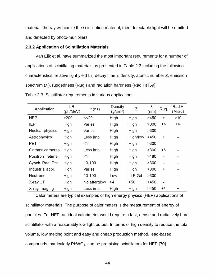
Van Eijk et al. have summarized the most important requirements for a number of
applications of scintillating materials as presented in Table 2.3 including the following
characteristics: relative light yield LR, decay time τ, density, atomic number Z, emission
spectrum (λr), ruggedness (Rug.) and radiation hardness (Rad H) [69].
Table 2-3. Scintillator requirements in various applications.
Calorimeters are typical examples of high energy physics (HEP) applications of
scintillator materials. The purpose of calorimeters is the measurement of energy of
particles. For HEP, an ideal calorimeter would require a fast, dense and radiatively hard
scintillator with a reasonably low light output. In terms of high density to reduce the total
volume, low melting point and easy and cheap production method, lead-based
compounds, particularly PbWO4, can be promising scintillators for HEP [70].
45
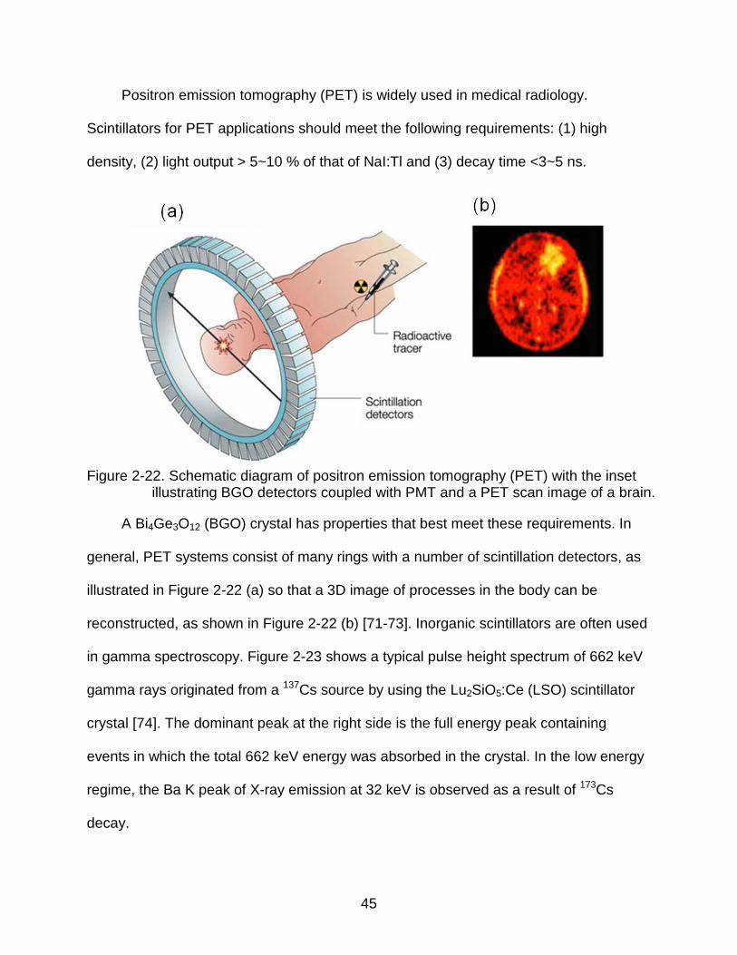
Positron emission tomography (PET) is widely used in medical radiology.
Scintillators for PET applications should meet the following requirements: (1) high
density, (2) light output > 5~10 % of that of NaI:Tl and (3) decay time <3~5 ns.
Figure 2-22. Schematic diagram of positron emission tomography (PET) with the inset illustrating BGO detectors coupled with PMT and a PET scan image of a brain.
A Bi4Ge3O12 (BGO) crystal has properties that best meet these requirements. In
general, PET systems consist of many rings with a number of scintillation detectors, as
illustrated in Figure 2-22 (a) so that a 3D image of processes in the body can be
reconstructed, as shown in Figure 2-22 (b) [71-73]. Inorganic scintillators are often used
in gamma spectroscopy. Figure 2-23 shows a typical pulse height spectrum of 662 keV
gamma rays originated from a 137Cs source by using the Lu2SiO5:Ce (LSO) scintillator
crystal [74]. The dominant peak at the right side is the full energy peak containing
events in which the total 662 keV energy was absorbed in the crystal. In the low energy
regime, the Ba K peak of X-ray emission at 32 keV is observed as a result of 173Cs
decay.

46
Figure 2-23. Pulse-height spectrum of a 137Cs source measured with a 100cm2 area and 2mm depth with LSO crystal coupled with a Hamamatsu R878 PMT.
2.4 Luminescent Nanoparticles
Low dimensional systems reviewed in this section are zero-dimensional (0-D)
systems, one-dimensional systems (1-D) and two-dimensional systems (2-D).
2.4.1 Fundamental and Application of Luminescent Nanoparticles
One of the most remarkable characteristics of luminescent nanoparticles with low
dimensions is their physical and optical modification through different distributions of
energy levels and densities of states. The origin of different quantum states is the
spatial confinement of electrons and holes inside the nanoparticles. The density of
stated of each low dimensional nanostructure can be describe by [75]:
ρ2D(E) = μπh�2
∑ θ(E − En − Eg)n (2-5)
ρ1D(E) = (2μ)1/2
πh�∑ 1
(E−Em−En−Eg)1/2m,n (2-6)
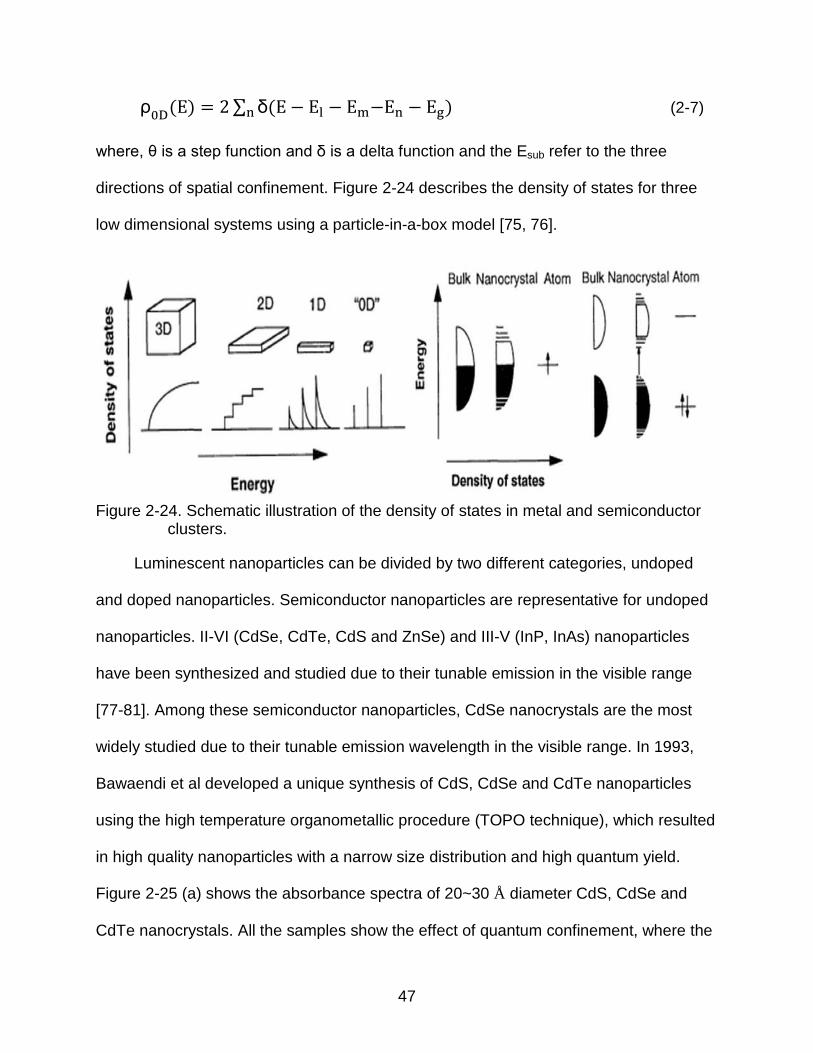
47
ρ0D(E) = 2∑ δ(E − El − Em−En − Eg)n (2-7)
where, θ is a step function and δ is a delta function and the Esub refer to the three
directions of spatial confinement. Figure 2-24 describes the density of states for three
low dimensional systems using a particle-in-a-box model [75, 76].
Figure 2-24. Schematic illustration of the density of states in metal and semiconductor clusters.
Luminescent nanoparticles can be divided by two different categories, undoped
and doped nanoparticles. Semiconductor nanoparticles are representative for undoped
nanoparticles. II-VI (CdSe, CdTe, CdS and ZnSe) and III-V (InP, InAs) nanoparticles
have been synthesized and studied due to their tunable emission in the visible range
[77-81]. Among these semiconductor nanoparticles, CdSe nanocrystals are the most
widely studied due to their tunable emission wavelength in the visible range. In 1993,
Bawaendi et al developed a unique synthesis of CdS, CdSe and CdTe nanoparticles
using the high temperature organometallic procedure (TOPO technique), which resulted
in high quality nanoparticles with a narrow size distribution and high quantum yield.
Figure 2-25 (a) shows the absorbance spectra of 20~30 Å diameter CdS, CdSe and
CdTe nanocrystals. All the samples show the effect of quantum confinement, where the
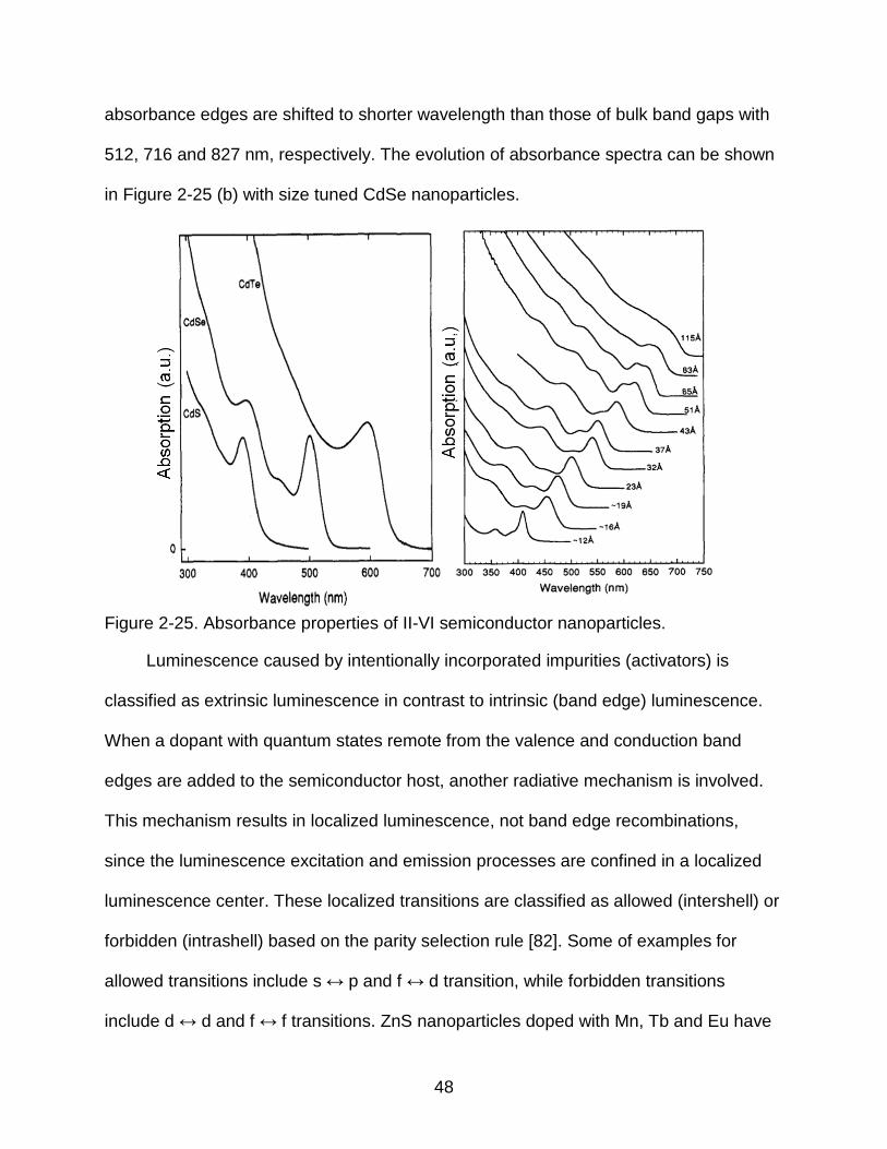
48
absorbance edges are shifted to shorter wavelength than those of bulk band gaps with
512, 716 and 827 nm, respectively. The evolution of absorbance spectra can be shown
in Figure 2-25 (b) with size tuned CdSe nanoparticles.
Figure 2-25. Absorbance properties of II-VI semiconductor nanoparticles.
Luminescence caused by intentionally incorporated impurities (activators) is
classified as extrinsic luminescence in contrast to intrinsic (band edge) luminescence.
When a dopant with quantum states remote from the valence and conduction band
edges are added to the semiconductor host, another radiative mechanism is involved.
This mechanism results in localized luminescence, not band edge recombinations,
since the luminescence excitation and emission processes are confined in a localized
luminescence center. These localized transitions are classified as allowed (intershell) or
forbidden (intrashell) based on the parity selection rule [82]. Some of examples for
allowed transitions include s ↔ p and f ↔ d transition, while forbidden transitions
include d ↔ d and f ↔ f transitions. ZnS nanoparticles doped with Mn, Tb and Eu have

49
been reported for the reduction of luminescent decay time [83, 84]. Rare-earth ions
doped oxide nanoparticles also have been widely studied. For example, Eu3+ or Nd3+
doped Gd2O3 nanoparticles have been used for cathodoluminescence and laser
applications [85, 86].
2.4.2 Surface Modification of Luminescent Nanoparticles
Figure 2-26. Schematic of organic and inorganic passivation.
The electronic and optical properties of all inorganic crystals depend on the three
dimensional periodicity of the potential wells that exist in the materials. The discontinuity
of periodicity at the surface layer will cause changes to these properties. The lack of
atoms on one side of the crystal leads to dangling chemical bonds that generate
structural modification such as reconstruction and relaxation [87]. To achieve stable
photoluminescence with a higher efficiency, passivation of the surface is crucial and it
has been successfully obtained by capping layers on the nanocores, as shown in Figure
2-26 [88].
50
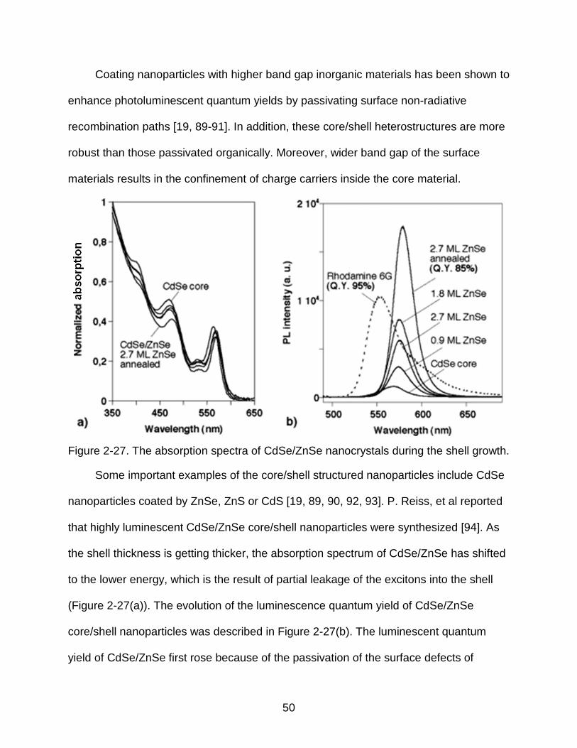
Coating nanoparticles with higher band gap inorganic materials has been shown to
enhance photoluminescent quantum yields by passivating surface non-radiative
recombination paths [19, 89-91]. In addition, these core/shell heterostructures are more
robust than those passivated organically. Moreover, wider band gap of the surface
materials results in the confinement of charge carriers inside the core material.
Figure 2-27. The absorption spectra of CdSe/ZnSe nanocrystals during the shell growth.
Some important examples of the core/shell structured nanoparticles include CdSe
nanoparticles coated by ZnSe, ZnS or CdS [19, 89, 90, 92, 93]. P. Reiss, et al reported
that highly luminescent CdSe/ZnSe core/shell nanoparticles were synthesized [94]. As
the shell thickness is getting thicker, the absorption spectrum of CdSe/ZnSe has shifted
to the lower energy, which is the result of partial leakage of the excitons into the shell
(Figure 2-27(a)). The evolution of the luminescence quantum yield of CdSe/ZnSe
core/shell nanoparticles was described in Figure 2-27(b). The luminescent quantum
yield of CdSe/ZnSe first rose because of the passivation of the surface defects of
51
nanocores, then decreased as a result of larger density of structural defects created in
the thick shells.
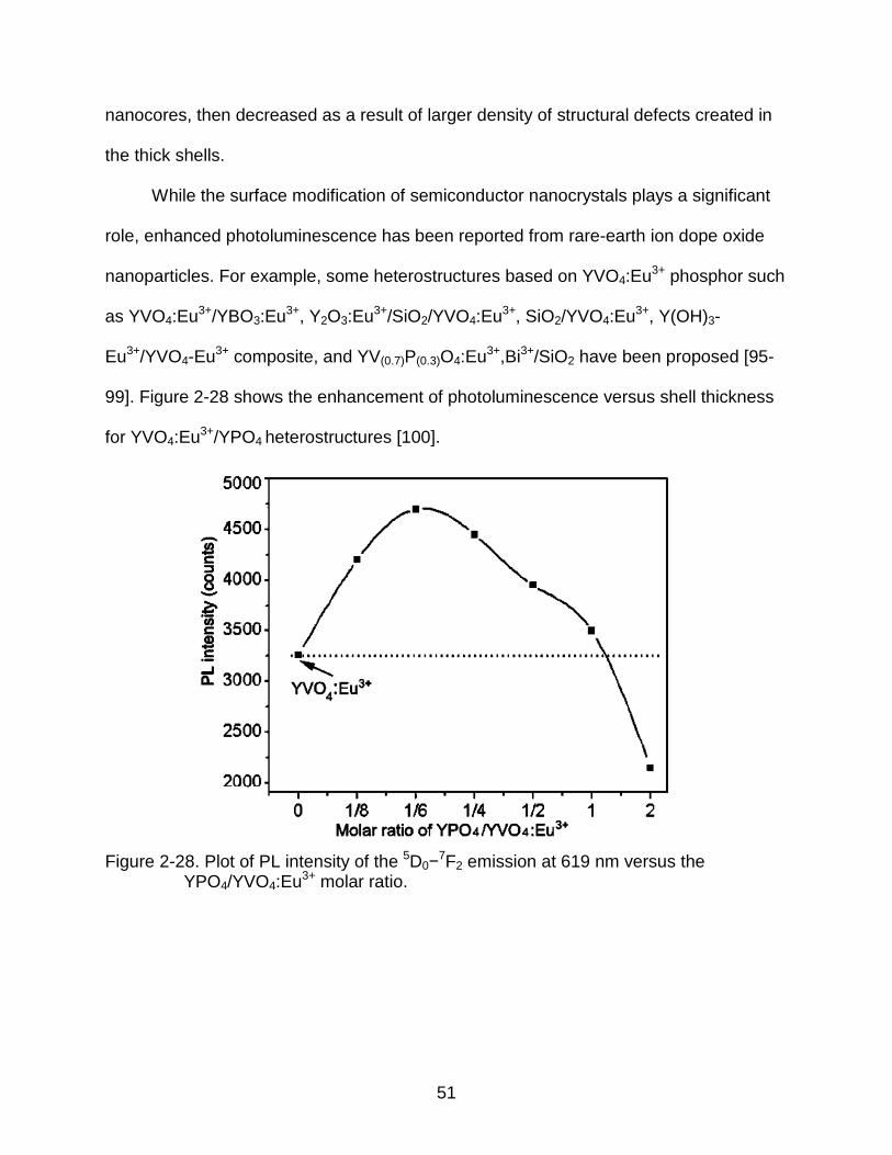
While the surface modification of semiconductor nanocrystals plays a significant
role, enhanced photoluminescence has been reported from rare-earth ion dope oxide
nanoparticles. For example, some heterostructures based on YVO4:Eu3+ phosphor such
as YVO4:Eu3+/YBO3:Eu3+, Y2O3:Eu3+/SiO2/YVO4:Eu3+, SiO2/YVO4:Eu3+, Y(OH)3-
Eu3+/YVO4-Eu3+ composite, and YV(0.7)P(0.3)O4:Eu3+,Bi3+/SiO2 have been proposed [95-
99]. Figure 2-28 shows the enhancement of photoluminescence versus shell thickness
for YVO4:Eu3+/YPO4 heterostructures [100].
Figure 2-28. Plot of PL intensity of the 5D0−7F2 emission at 619 nm versus the YPO4/YVO4:Eu3+ molar ratio.
52
CHAPTER 3 SHAPE CONTROLLED GADOLINIUM OXIDE DOPED WITH EUROPIUM COLLOIDAL
NANOCRYSTALS GROWN BY HOT-SOLUTION METHOD
3.1 Introduction
Rare-earth doped luminescent nanocrystals are being intensively studied due to
their potential applications in displays, lightings and biologic diagnostics [101, 102].It is
well established that the optical, electrical and chemical properties of nanoparticles
depend strongly on their shape, morphology and crystal structure [103-105]. Zero- and
one-dimensional (1D) nanostructures, such as quantum dots, nano-rods, nano-wires
and nano-tubes, have been widely studied [106, 107]. Specific organic surfactants,
which can modulate the growth kinetics, have been employed to grow anisotropic
luminescent nanostructures using non-hydrolytic procedures with and without templates
[108-110]. For example, rare earth doped zero and one dimensional (0D and 1D)
structures such as LaPO4: RE ( RE= Eu3+, Tb3+) nanowires, Y2O3:RE nanotubes and
Gd2O3: Eu3+ nanoplates have been reported [25, 111-114]. Colloidal growth in non-
hydrolytic liquid media can give reproducible shapes and sizes of nanoparticles. This
synthesis route results in nanonarticles (NPs) with sizes tuned over the 1–10 nm range.
These NPs can be dispersed in organic media for numerous potential applications [115,
116].
Rare-earth doped gadolinium oxide (Gd2O3) generally exhibit photoluminescence
(PL) with high quantum yields. For example, Eu3+ doped gadolinium oxide exhibits red
luminescence due to the electric dipole 5D0–7F2 transitions on the trivalent europium ion
(Eu3+, 4f6) [47]. Gd2O3:Eu3+ nanocrystals produced by non-hydrolytic thermal reactions
in the presence of organic surfactants exhibit intense luminescence, and is crystalline
and mono-dispersed. Furthermore, this synthetic route allows control of the shape of
53
nanoparticles through the use of processing parameters such as precursor types,
precursor concentration, surfactant, solvent and reaction temperature and time [16]. In
this chapter, the luminescent properties of Gd2O3:Eu3+ will be reported and discussed
with respect to the crystal structure, shapes of nanoparticles and the Eu3+ dopant
location in the Gd2O3 host.
3.2 Experimental
3.2.1 Materials
The following precursor compounds and solvents were purchased from Aldrich
Chemical Co. : Gd(III) acetylacetonate hydrate, Eu(III) acetate hydrate, oleic acid (90% ,
tech.), Eu(III) acetate hydrate (90% , tech.), oleic acid (90%, tech.), oleyamine (70%),
benzyl ether (99%) and 1,2-hexadecanediol (HDD, 97%). All chemicals were used
without further purification. Absolute ethanol, benzyl ether and hexane were analytical
grade and used as received.
3.2.2 Gd2O3:Eu3+ Nanocrystal Synthesis
In a one-pot hot-solution synthesis method for the growth of Gd2O3:Eu3+
nanocrystals, Gd-acetylacetonate (3 mmol) and Eu-acetate (0.6 mmol) were mixed and
dehydrated at 120 °C for 6 hours, followed by addition of oleic acid (9 mmol), oleylamine
(9 mmol), benzyl ether (15 mmol) and hexadecanediol (3mmol). The precursor solution
was transferred and vigorously stirred under UHP N2 gas ambient in a three-neck flask
surrounded by a heating mantle. The mixture was held at 120 °C for 30 min, resulting in
a transparent yellowish solution. In some cases, samples were preheated to 200 °C for
30 min to change the shape of the nanocrystals. After preheating, the temperature was
increased to 290~320 °C with a heating rate of 5~25 °C/min, and the steady-state
condition was maintained for 30 to 180 min. The color of the mixture changed to deep
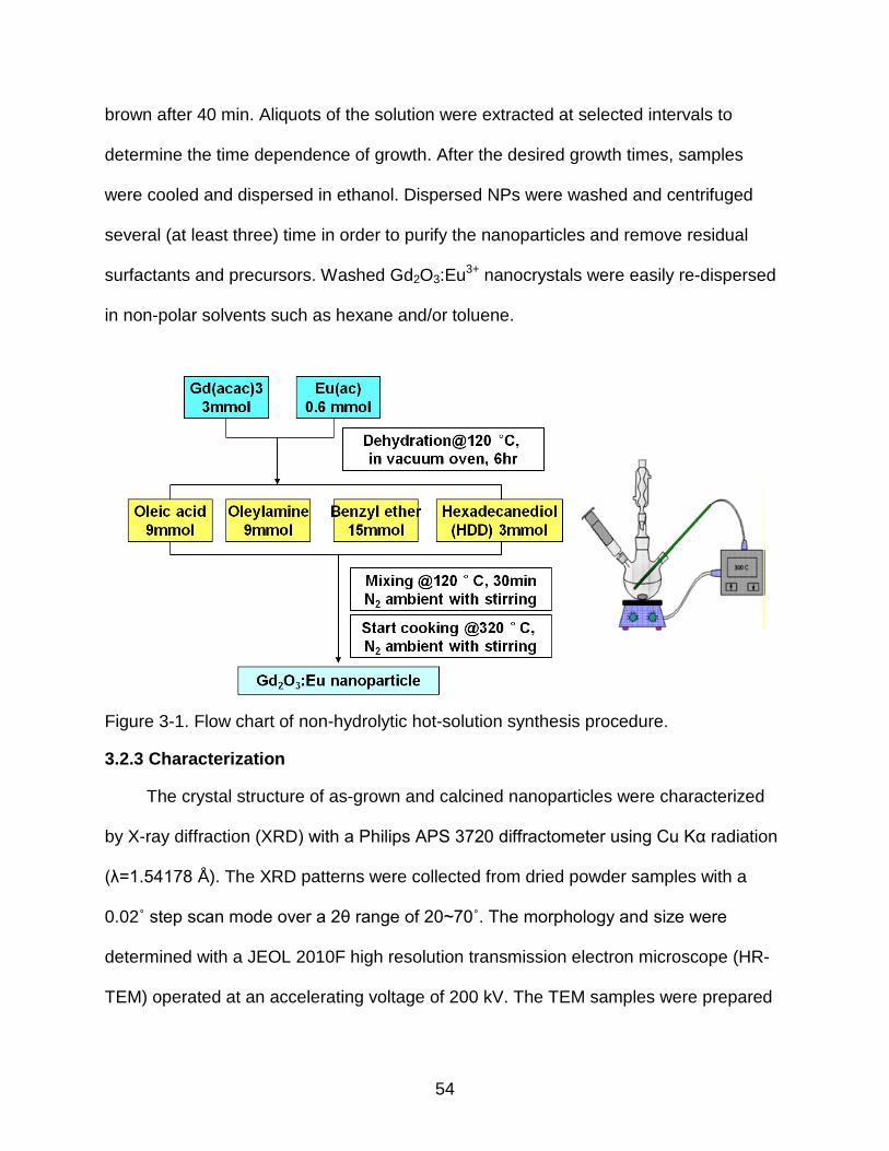
54
brown after 40 min. Aliquots of the solution were extracted at selected intervals to
determine the time dependence of growth. After the desired growth times, samples
were cooled and dispersed in ethanol. Dispersed NPs were washed and centrifuged
several (at least three) time in order to purify the nanoparticles and remove residual
surfactants and precursors. Washed Gd2O3:Eu3+ nanocrystals were easily re-dispersed
in non-polar solvents such as hexane and/or toluene.
Figure 3-1. Flow chart of non-hydrolytic hot-solution synthesis procedure.
3.2.3 Characterization
The crystal structure of as-grown and calcined nanoparticles were characterized
by X-ray diffraction (XRD) with a Philips APS 3720 diffractometer using Cu Kα radiation
(λ=1.54178 Å). The XRD patterns were collected from dried powder samples with a
0.02˚ step scan mode over a 2θ range of 20~70˚. The morphology and size were
determined with a JEOL 2010F high resolution transmission electron microscope (HR-
TEM) operated at an accelerating voltage of 200 kV. The TEM samples were prepared
55
by drop-casting NPs dispersed in hexane onto a carbon coated holey copper grids,
followed by drying at room temperature. Photoluminescence (PL) and photo-
luminescence excitation (PLE) spectra were measured at room temperature using a
JASCO FP-6500/6600 research grade fluorescence spectrometer with a 150 W Xenon
lamp. The quantum yields were determined by comparing the integrated emission from
colloidal NP solutions with those from an ethanol-Rhodamine 6G solution growth the
same optical density and excited at the same wavelength of 280 nm. The
concentrations of Eu3+ dopant in as-prepared Gd2O3:Eu3+ nanoparticles were measured
using an inductively coupled plasma (ICP) spectrometer (Perkin-Elmer Plasma 3200).
X-ray luminescence was measured with a 40 kV BulletTM X-ray tube combined with a
Ocean Optics USB-2000 miniature fiber optic spectrometer. The distance from the x-ray
target to the sample was ~3 cm and the x-ray tube was operated at 100 μA. For each
measurement, a crucible with 57 mm2 area and 2 mm thickness was filled with
nanopowder such that each sample had the same area exposed to the x-rays.
3.3 Results and Discussion
3.3.1 Shape Control of Gd2O3:Eu3+ Nanocrystals
Three distinct shapes, clover, plate and round, of nanoparticles were observed for
the present precursors and one-pot hot-solution method. Typical NPs are shown in the
high resolution TEM images of Figure 3-2. The preheat and, reaction times and
temperatures, and observed shapes are summarized in Table 1. Figure 3-2(a) shows
~20 nm clover Gd2O3:Eu3+ nanoparticles, with each nanoparticle being composed of
several petals that self- assembles into the clover NPs, which were grown with a
preheating step. Square and round nanoparticles with characteristic dimensions of 10-
15 nm are shown in Figure 3-2 (b-d).
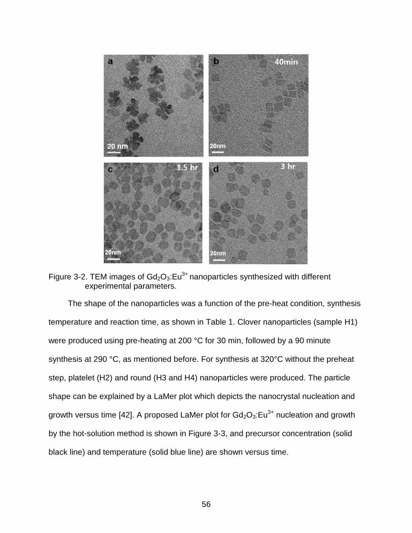
56
Figure 3-2. TEM images of Gd2O3:Eu3+ nanoparticles synthesized with different experimental parameters.
The shape of the nanoparticles was a function of the pre-heat condition, synthesis
temperature and reaction time, as shown in Table 1. Clover nanoparticles (sample H1)
were produced using pre-heating at 200 °C for 30 min, followed by a 90 minute
synthesis at 290 °C, as mentioned before. For synthesis at 320°C without the preheat
step, platelet (H2) and round (H3 and H4) nanoparticles were produced. The particle
shape can be explained by a LaMer plot which depicts the nanocrystal nucleation and
growth versus time [42]. A proposed LaMer plot for Gd2O3:Eu3+ nucleation and growth
by the hot-solution method is shown in Figure 3-3, and precursor concentration (solid
black line) and temperature (solid blue line) are shown versus time.
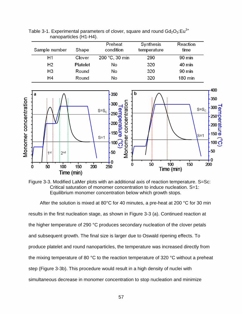
57
Table 3-1. Experimental parameters of clover, square and round Gd2O3:Eu3+
nanoparticles (H1-H4).
Figure 3-3. Modified LaMer plots with an additional axis of reaction temperature. S=Sc: Critical saturation of monomer concentration to induce nucleation. S=1: Equilibrium monomer concentration below which growth stops.
After the solution is mixed at 80°C for 40 minutes, a pre-heat at 200 °C for 30 min
results in the first nucleation stage, as shown in Figure 3-3 (a). Continued reaction at
the higher temperature of 290 °C produces secondary nucleation of the clover petals
and subsequent growth. The final size is larger due to Oswald ripening effects. To
produce platelet and round nanoparticles, the temperature was increased directly from
the mixing temperature of 80 °C to the reaction temperature of 320 °C without a preheat
step (Figure 3-3b). This procedure would result in a high density of nuclei with
simultaneous decrease in monomer concentration to stop nucleation and minimize
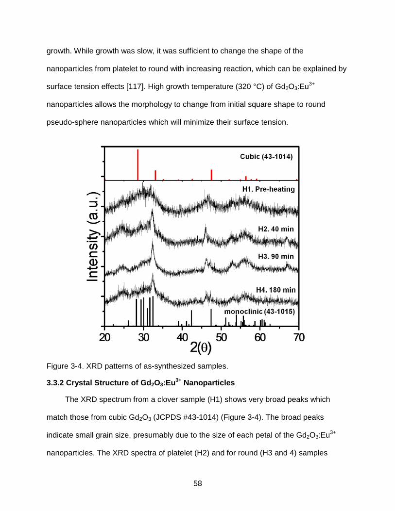
58
growth. While growth was slow, it was sufficient to change the shape of the
nanoparticles from platelet to round with increasing reaction, which can be explained by
surface tension effects [117]. High growth temperature (320 °C) of Gd2O3:Eu3+
nanoparticles allows the morphology to change from initial square shape to round
pseudo-sphere nanoparticles which will minimize their surface tension.
Figure 3-4. XRD patterns of as-synthesized samples.
3.3.2 Crystal Structure of Gd2O3:Eu3+ Nanoparticles
The XRD spectrum from a clover sample (H1) shows very broad peaks which
match those from cubic Gd2O3 (JCPDS #43-1014) (Figure 3-4). The broad peaks
indicate small grain size, presumably due to the size of each petal of the Gd2O3:Eu3+
nanoparticles. The XRD spectra of platelet (H2) and for round (H3 and 4) samples
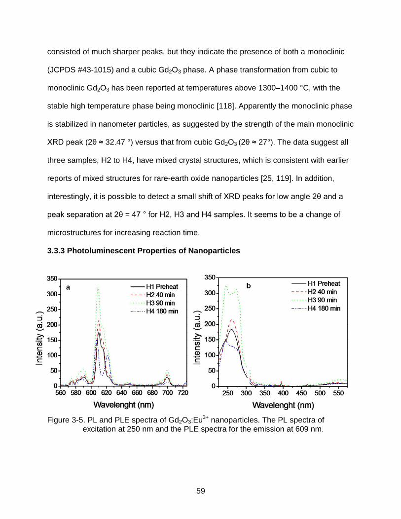
59
consisted of much sharper peaks, but they indicate the presence of both a monoclinic
(JCPDS #43-1015) and a cubic Gd2O3 phase. A phase transformation from cubic to
monoclinic Gd2O3 has been reported at temperatures above 1300–1400 °C, with the
stable high temperature phase being monoclinic [118]. Apparently the monoclinic phase
is stabilized in nanometer particles, as suggested by the strength of the main monoclinic
XRD peak (2θ ≈ 32.47 °) versus that from cubic Gd2O3 (2θ ≈ 27°). The data suggest all
three samples, H2 to H4, have mixed crystal structures, which is consistent with earlier
reports of mixed structures for rare-earth oxide nanoparticles [25, 119]. In addition,
interestingly, it is possible to detect a small shift of XRD peaks for low angle 2θ and a
peak separation at 2θ = 47 ° for H2, H3 and H4 samples. It seems to be a change of
microstructures for increasing reaction time.
3.3.3 Photoluminescent Properties of Nanoparticles
Figure 3-5. PL and PLE spectra of Gd2O3:Eu3+ nanoparticles. The PL spectra of excitation at 250 nm and the PLE spectra for the emission at 609 nm.
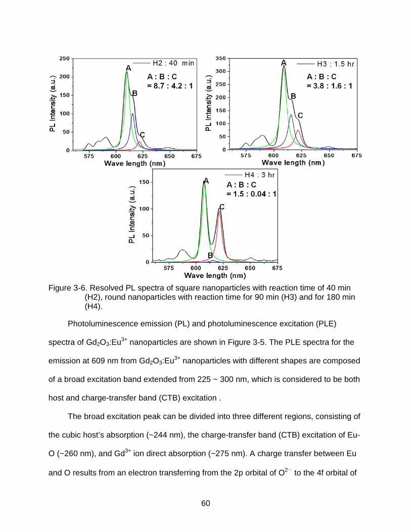
60
Figure 3-6. Resolved PL spectra of square nanoparticles with reaction time of 40 min (H2), round nanoparticles with reaction time for 90 min (H3) and for 180 min (H4).
Photoluminescence emission (PL) and photoluminescence excitation (PLE)
spectra of Gd2O3:Eu3+ nanoparticles are shown in Figure 3-5. The PLE spectra for the
emission at 609 nm from Gd2O3:Eu3+ nanoparticles with different shapes are composed
of a broad excitation band extended from 225 ~ 300 nm, which is considered to be both
host and charge-transfer band (CTB) excitation .
The broad excitation peak can be divided into three different regions, consisting of
the cubic host’s absorption (~244 nm), the charge-transfer band (CTB) excitation of Eu-
O (~260 nm), and Gd3+ ion direct absorption (~275 nm). A charge transfer between Eu
and O results from an electron transferring from the 2p orbital of O2− to the 4f orbital of

61
Eu3+. The strength of the charge transfer is related to the covalency of the O2− - Eu3+
bond and the coordination of the Eu3+ and Gd3+ ions [120]. The small, sharp peaks
between 360 and 530 nm and Figure 3-5b are from direct excitation of the f–f shell
transitions on Eu3+ ions [121]. As discussed above, PL excitation spectra of Gd2O3:Eu3+
nanoparticles have three different components, such as host absorption, CTB and Gd3+
direct absorption, so that it is possible to decompose the broad PL excitation peak from
225 to 300 nm into three Lorentzian curves. Their different ratio show that H3 and H4
exhibit higher host and Gd3+ absorption whereas H1 and H2 has a dominant CTB
excitation [122, 123].
Growth at low temperature for short reaction times presumably result in more
defected crystalline and low host and Gd3+ absorption. The PL emission spectra from
Gd2O3:Eu3+ nanoparticles with various shapes is dominated by the 5D0-7F2 transition at
609 nm with minor peaks from 5D0-7FJ (J = 0, 1, 3 and 4) transitions, which is a
characteristic of the Gd2O3 host lattice [47]. It was previously reported that several split
levels give rise to several PL peaks between 600 and 630 nm in monoclinic Gd2O3:Eu3+,
while the 5D0-7F2 peak at 610 nm is dominant from cubic Gd2O3 [124, 125]. As shown in
Figure 3-6, the PL spectra between 600-625 nm from Gd2O3:Eu3+ nanoparticles without
pre-heating (H2, H3 and H4) can be resolved into three different peaks (A, B and C,
centered at 610, 615 and 621 nm), where A is from the cubic phase (610 nm), and B
and C are from the monoclinic phase (615 and 621 nm). The ratio of the three peak
intensities normalized to the intensity of peak C is shown in Figure 3-6. The
photoluminescence properties is dependent on the structure of host material [47].
Generally, cubic Gd2O3:Eu3+ exhibits brighter luminescence than does monoclinic
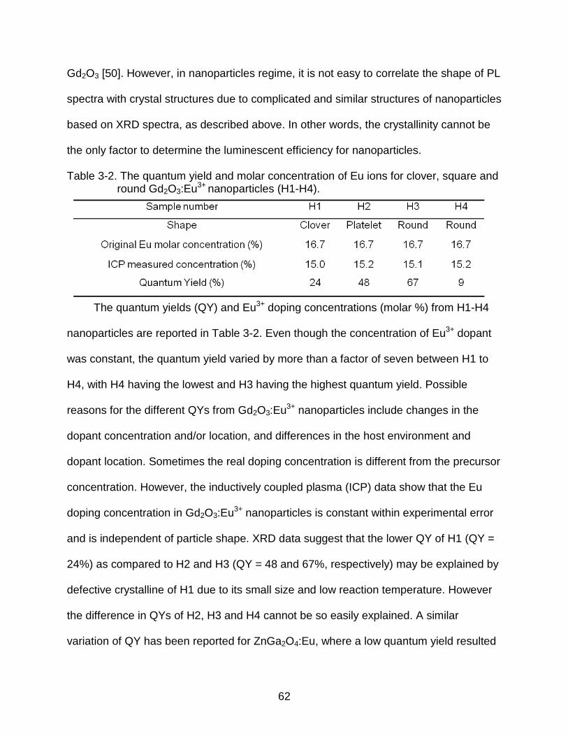
62
Gd2O3 [50]. However, in nanoparticles regime, it is not easy to correlate the shape of PL
spectra with crystal structures due to complicated and similar structures of nanoparticles
based on XRD spectra, as described above. In other words, the crystallinity cannot be
the only factor to determine the luminescent efficiency for nanoparticles.
Table 3-2. The quantum yield and molar concentration of Eu ions for clover, square and round Gd2O3:Eu3+ nanoparticles (H1-H4).
The quantum yields (QY) and Eu3+ doping concentrations (molar %) from H1-H4
nanoparticles are reported in Table 3-2. Even though the concentration of Eu3+ dopant
was constant, the quantum yield varied by more than a factor of seven between H1 to
H4, with H4 having the lowest and H3 having the highest quantum yield. Possible
reasons for the different QYs from Gd2O3:Eu3+ nanoparticles include changes in the
dopant concentration and/or location, and differences in the host environment and
dopant location. Sometimes the real doping concentration is different from the precursor
concentration. However, the inductively coupled plasma (ICP) data show that the Eu
doping concentration in Gd2O3:Eu3+ nanoparticles is constant within experimental error
and is independent of particle shape. XRD data suggest that the lower QY of H1 (QY =
24%) as compared to H2 and H3 (QY = 48 and 67%, respectively) may be explained by
defective crystalline of H1 due to its small size and low reaction temperature. However
the difference in QYs of H2, H3 and H4 cannot be so easily explained. A similar
variation of QY has been reported for ZnGa2O4:Eu, where a low quantum yield resulted
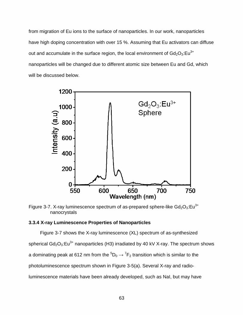
63
from migration of Eu ions to the surface of nanoparticles. In our work, nanoparticles
have high doping concentration with over 15 %. Assuming that Eu activators can diffuse
out and accumulate in the surface region, the local environment of Gd2O3:Eu3+
nanoparticles will be changed due to different atomic size between Eu and Gd, which
will be discussed below.
Figure 3-7. X-ray luminescence spectrum of as-prepared sphere-like Gd2O3:Eu3+ nanocrystals
3.3.4 X-ray Luminescence Properties of Nanoparticles
Figure 3-7 shows the X-ray luminescence (XL) spectrum of as-synthesized
spherical Gd2O3:Eu3+ nanoparticles (H3) irradiated by 40 kV X-ray. The spectrum shows
a dominating peak at 612 nm from the 5D0 → 7F2 transition which is similar to the
photoluminescence spectrum shown in Figure 3-5(a). Several X-ray and radio-
luminescence materials have been already developed, such as NaI, but may have
64
undesirable properties, such as poor high temperature drift effects. In this study, X-ray
luminescence was observed from Gd2O3:Eu3+ nanoparticles synthesized by non-
hydrolytic hot-solution synthesis method, consistent with its potential application as
scintillation detectors.
3.4 Conclusion
Eu3+ doped Gd2O3 nanoparticles were synthesized by a hot-solution method. The
shape of Gd2O3:Eu3+ nanoparticles that were preheated and then reacted 290° C was
“clover”. Without the preheat step and for reaction at 320° C, short times produced
platelet nanoparticles, but became more circular at longer reaction times. Potential
mechanisms leading to various shapes of Gd2O3:Eu3+ nanoparticles were discussed. By
controlling reaction parameters, the quantum yield of Gd2O3:Eu3+ nanoparticles also
varied from 9 % to 67 %. Clover and plate Gd2O3:Eu3+ nanoparticles exhibited relatively
low quantum yield, 24% and 48%, respectively, because of the defective crystalline.
Round Gd2O3:Eu3+ nanoparticles with 1.5 hrs reaction time showed the highest
quantum yield of 67 %, which results from the combination of two factors, a host
environment and a dopant location. For Eu3+ doped nanoparticles with a prolonged
reaction time with 3 hrs, the quantum yield decreased to 9% presumably due to the
migration of dopant ions and subsequent segregation to the nanoparticle surface region.
65
CHAPTER 4 ENHANCED PHOTOLUMINESCENCE FROM GADOLINIUM OXIDE DOPED WITH
EUROPIUM NANOCORES WITH YTTRIUM OIXDE THIN SHELL
4.1 Introduction
Oxide and sulphide nanophosphors are popular research topics due to their
unique physical properties. The size, shape, structure and composition of nanoparticles
can be controlled so that their optical, electrical or mechanical properties can be tuned
to desired values [76, 126]. For example, oxide nanophosphors, such as Y2O3, GdVO4
and Gd2O3 doped with rare earth ions have been studied for plasma display panels
(PDPs), cathode ray tubes (CRTs) and field emission displays (FEDs) [127-129].
Europium doped Gd2O3 exhibits red luminescence from the electric dipole 5D0-7F2
transitions on the trivalent europium ions (Eu3+ 4f6) [47]. Gd2O3:Eu3+ nanoparticles
synthesized by hydrothermal or nonhydrolytic thermal reactions with organic surfactants
exhibit excellent crystallinity and good photoluminescence (PL) efficiency (QY = ~50%)
[25]. Moreover, the rate of growth and the shape of nanoparticles can be controlled by
the type and concentration of precursors and organic surfactants [25, 130]. However, it
is well known that states at the surface of phosphor powders can lead to non-radiative
relaxation and low luminescent efficiencies [87], especially for nanophosphors with a
large surface to volume ratio. Capping of the nanoparticles core with the proper shell
materials could passivate surface defects and eliminate the non-radiative pathways
[131]. This strategy has been successfully used in core/shell nanoparticles such as
CdSe/ZnS and CdS/ZnS, as well as oxide nanoparticles like SiO2/Gd2O3:Eu3+ [132-134].
The precipitation of nanoparticles in a high boiling-point alcohol, generally called
the polyol synthesis method, has been used to produce various materials including
elemental metals and oxides [135, 136]. Recently, Wang, et al reported the synthesis of
66
CeF3 core/shell nanoparticles using the polyol method [137]. In this study, the polyol
method was used to synthesize Gd2O3:Eu3+ cores followed by nucleation and growth of
Y2O3. It will be shown that only a fraction of the Y2O3 grew as a shell on the Gd2O3:Eu3+
cores, but the shell did increase the PL intensity. The consequences of growth of yttria
both as a shell and as a separate phase on the properties of the nanophosphor were
investigated.
4.2 Experimental
The following precursor compounds and solvents were purchased from Aldrich
Chemical Co. : Gd(III) nitrate hydrate (99.9%), Eu(III) nitrate hexahydrate (99.9%), Y(III)
nitrate (99.9%), and ethylene glycol (99%). All chemicals were analytical grade and
were used without further purification.
4.2.1 Synthesis of Gd2O3:Eu3+ Nanocores
The doping concentration of Eu3+ in the Gd2O3 host was 5 mol% based on
precursor concentrations. For synthesis, 1.9mmol of Gd(NO3)3·6H2O and 0.1 mmol
Eu(NO3)3·6H2O were dissolved in 25ml of ethylene glycol (EG) in a stirred round-
bottomed flask at 100 ˚C. The clear solution was then heated to 180 ˚C for 1hr with
vigorous stirring. The resulting suspension was cooled to room temperature, diluted with
ethanol and the nanoparticles separated by centrifugation at 7000 rpm. To remove
unreacted precursor and EG, the nanoparticles were redispersed in ethanol and
centrifuged at least three times. The nanoparticles were calcined at 600 ˚C for 2 h in air.
4.2.2 Synthesis of Y2O3 in the Presence of Gd2O3:Eu3+ Nanocores
Growth of Gd1.9O3:Eu0.13+/Y2O3 core/shell nanoparticles was attempted with a two-
step process. First, Gd2O3:Eu3+ core nanoparticles were prepared using the procedure
described above, then washed with ethanol at least three times. The quantity of Y2O3,

67
and therefore the shell thicknesses, was varied in the second step by changing the
precursor molar ratio, R, of Y(NO3)3·6H2O to (Gd+Eu)(NO3) 3·6H2O from R=1:16 to 1:8,
1:4 and 1:1. As an example, for R = 1:1, Gd2O3:Eu3+ nanocores were obtained from
2mmol of (Gd+Eu)(NO3) 3·6H2O in a first step, then 2 mmol of Y(NO3)3·6H2O were
added to 25 mL of EG at 100 ˚C and Y2O3 was grown in a second step. This solution
was heated to 180 ˚C for 2h with vigorous stirring, cooled to room temperature, washed
and centrifuged as discussed above.
4.2.3 Characterization of Nanoparticles
The crystal structure of as-grown and calcined nanoparticles were characterized
by X-ray diffraction (XRD) with a Philips APS 3720 diffractometer using Cu Kα radiation
(λ=1.54178 Å). The XRD patterns were collected from dried powder samples with a
0.02˚ step scan mode over a 2θ range of 20~70˚. Morphology and size of nanoparticles
were obtained by using a JEOL 2010F high resolution transmission electron microscope
(HR-TEM) operated at an accelerating voltage of 200 kV. Specimens for the TEM were
prepared by drop-casting particles dispersed in ethanol onto holey carbon-coated
copper grids.
X-ray photoelectron spectroscopy (XPS) was used to analyze the nanoparticle’s
shell thickness with a Perkin-Elmer PHI 5100 ESCA system and Al Kα X-rays
(E=1.486keV). All the XPS peaks were referenced to the C1s peak at 284.6 eV. To
make XPS samples, the same weight of nanoparticles were dispersed in ethanol and
50μl of solution was drop-cast onto 1cm2 Si wafers. Photoluminescence (PL) and photo-
luminescence excitation (PLE) spectra and luminescent relaxation lifetimes were
measured at room temperature using a JASCO FP-6500/6600 research grade
fluorescence spectrometer with a 150 W Xenon lamp using films on quartz slides drop
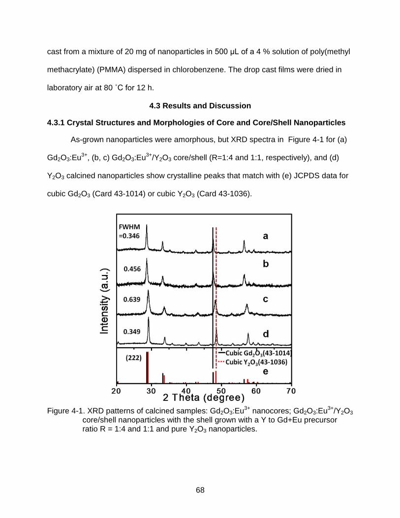
68
cast from a mixture of 20 mg of nanoparticles in 500 μL of a 4 % solution of poly(methyl
methacrylate) (PMMA) dispersed in chlorobenzene. The drop cast films were dried in
laboratory air at 80 ˚C for 12 h.
4.3 Results and Discussion
4.3.1 Crystal Structures and Morphologies of Core and Core/Shell Nanoparticles
As-grown nanoparticles were amorphous, but XRD spectra in Figure 4-1 for (a)
Gd2O3:Eu3+, (b, c) Gd2O3:Eu3+/Y2O3 core/shell (R=1:4 and 1:1, respectively), and (d)
Y2O3 calcined nanoparticles show crystalline peaks that match with (e) JCPDS data for
cubic Gd2O3 (Card 43-1014) or cubic Y2O3 (Card 43-1036).
Figure 4-1. XRD patterns of calcined samples: Gd2O3:Eu3+ nanocores; Gd2O3:Eu3+/Y2O3 core/shell nanoparticles with the shell grown with a Y to Gd+Eu precursor ratio R = 1:4 and 1:1 and pure Y2O3 nanoparticles.
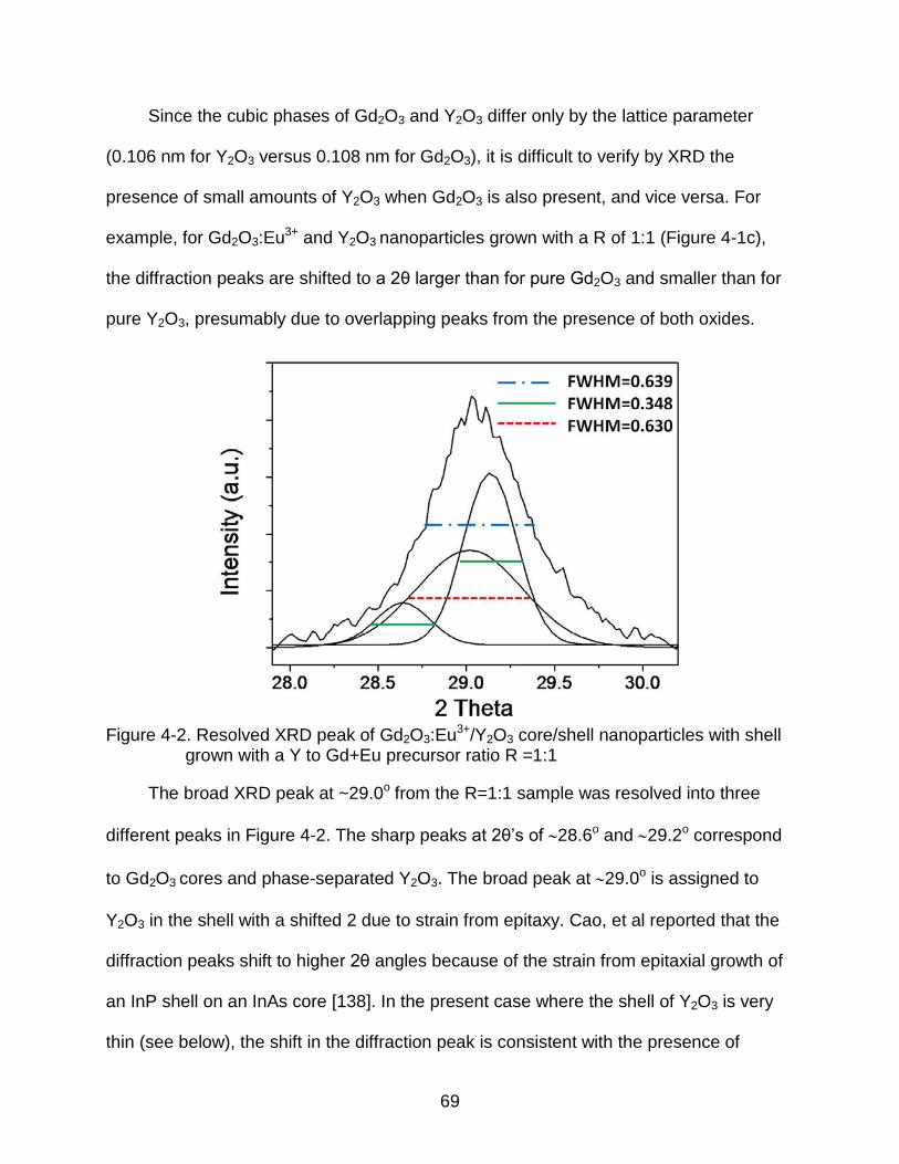
69
Since the cubic phases of Gd2O3 and Y2O3 differ only by the lattice parameter
(0.106 nm for Y2O3 versus 0.108 nm for Gd2O3), it is difficult to verify by XRD the
presence of small amounts of Y2O3 when Gd2O3 is also present, and vice versa. For
example, for Gd2O3:Eu3+ and Y2O3 nanoparticles grown with a R of 1:1 (Figure 4-1c),
the diffraction peaks are shifted to a 2θ larger than for pure Gd2O3 and smaller than for
pure Y2O3, presumably due to overlapping peaks from the presence of both oxides.
Figure 4-2. Resolved XRD peak of Gd2O3:Eu3+/Y2O3 core/shell nanoparticles with shell grown with a Y to Gd+Eu precursor ratio R =1:1
The broad XRD peak at ~29.0o from the R=1:1 sample was resolved into three
different peaks in Figure 4-2. The sharp peaks at 2θ’s of ∼28.6o and ∼29.2o correspond
to Gd2O3 cores and phase-separated Y2O3. The broad peak at ∼29.0o is assigned to
Y2O3 in the shell with a shifted 2 due to strain from epitaxy. Cao, et al reported that the
diffraction peaks shift to higher 2θ angles because of the strain from epitaxial growth of
an InP shell on an InAs core [138]. In the present case where the shell of Y2O3 is very
thin (see below), the shift in the diffraction peak is consistent with the presence of
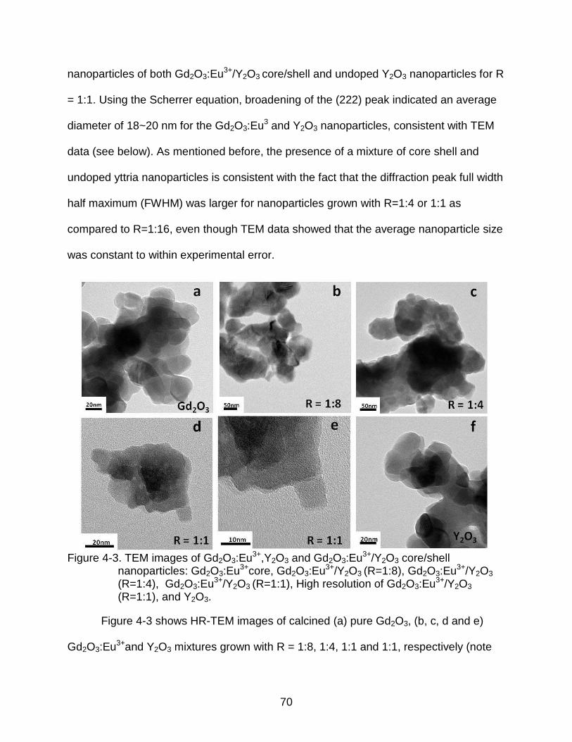
70
nanoparticles of both Gd2O3:Eu3+/Y2O3 core/shell and undoped Y2O3 nanoparticles for R
= 1:1. Using the Scherrer equation, broadening of the (222) peak indicated an average
diameter of 18~20 nm for the Gd2O3:Eu3 and Y2O3 nanoparticles, consistent with TEM
data (see below). As mentioned before, the presence of a mixture of core shell and
undoped yttria nanoparticles is consistent with the fact that the diffraction peak full width
half maximum (FWHM) was larger for nanoparticles grown with R=1:4 or 1:1 as
compared to R=1:16, even though TEM data showed that the average nanoparticle size
was constant to within experimental error.
Figure 4-3. TEM images of Gd2O3:Eu3+,Y2O3 and Gd2O3:Eu3+/Y2O3 core/shell nanoparticles: Gd2O3:Eu3+core, Gd2O3:Eu3+/Y2O3 (R=1:8), Gd2O3:Eu3+/Y2O3 (R=1:4), Gd2O3:Eu3+/Y2O3 (R=1:1), High resolution of Gd2O3:Eu3+/Y2O3 (R=1:1), and Y2O3.
Figure 4-3 shows HR-TEM images of calcined (a) pure Gd2O3, (b, c, d and e)
Gd2O3:Eu3+and Y2O3 mixtures grown with R = 1:8, 1:4, 1:1 and 1:1, respectively (note
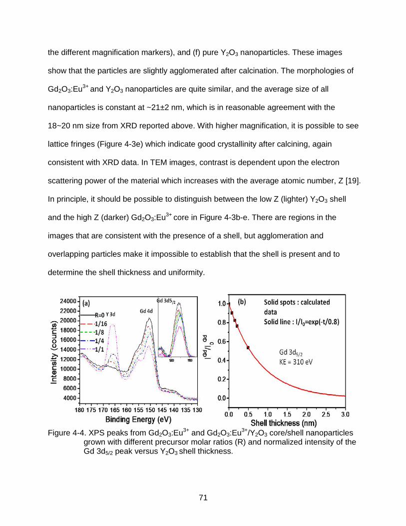
71
the different magnification markers), and (f) pure Y2O3 nanoparticles. These images
show that the particles are slightly agglomerated after calcination. The morphologies of
Gd2O3:Eu3+ and Y2O3 nanoparticles are quite similar, and the average size of all
nanoparticles is constant at ~21±2 nm, which is in reasonable agreement with the
18~20 nm size from XRD reported above. With higher magnification, it is possible to see
lattice fringes (Figure 4-3e) which indicate good crystallinity after calcining, again
consistent with XRD data. In TEM images, contrast is dependent upon the electron
scattering power of the material which increases with the average atomic number, Z [19].
In principle, it should be possible to distinguish between the low Z (lighter) Y2O3 shell
and the high Z (darker) Gd2O3:Eu3+ core in Figure 4-3b-e. There are regions in the
images that are consistent with the presence of a shell, but agglomeration and
overlapping particles make it impossible to establish that the shell is present and to
determine the shell thickness and uniformity.
Figure 4-4. XPS peaks from Gd2O3:Eu3+ and Gd2O3:Eu3+/Y2O3 core/shell nanoparticles grown with different precursor molar ratios (R) and normalized intensity of the Gd 3d5/2 peak versus Y2O3 shell thickness.
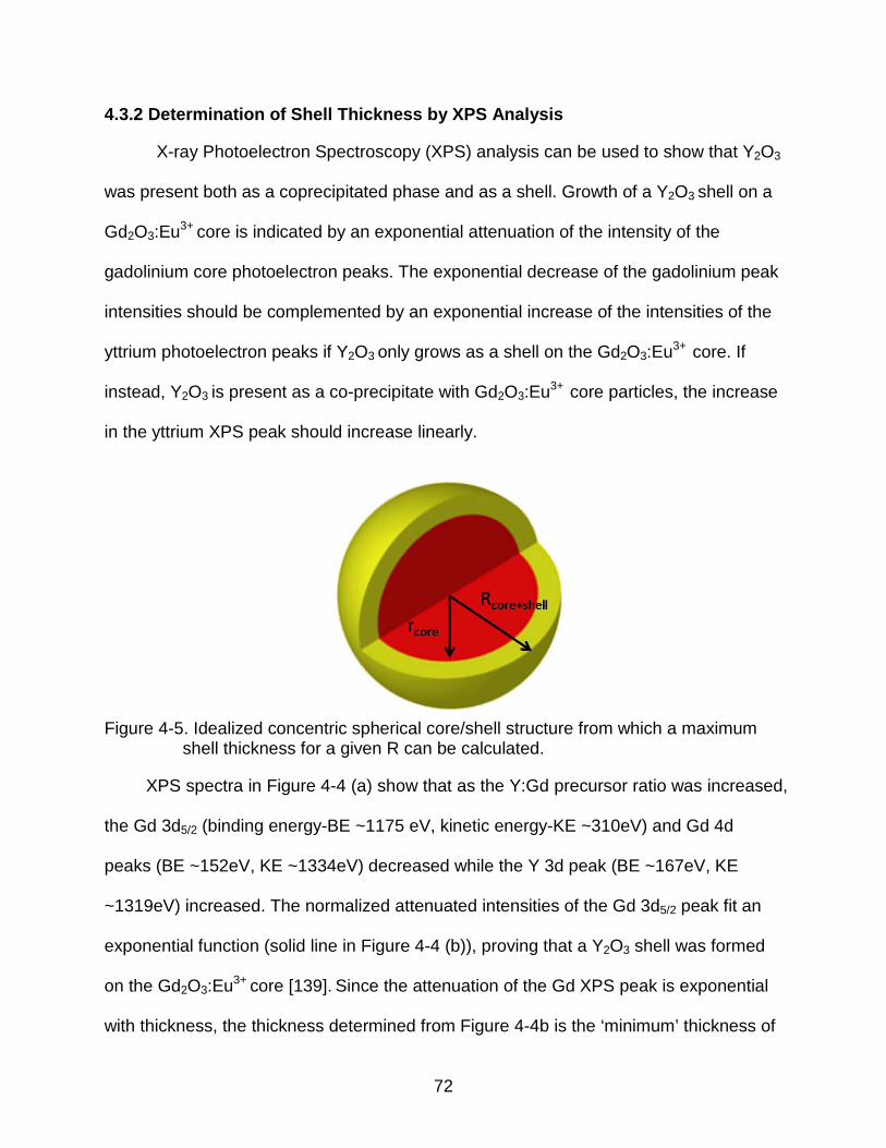
72
4.3.2 Determination of Shell Thickness by XPS Analysis
X-ray Photoelectron Spectroscopy (XPS) analysis can be used to show that Y2O3
was present both as a coprecipitated phase and as a shell. Growth of a Y2O3 shell on a
Gd2O3:Eu3+ core is indicated by an exponential attenuation of the intensity of the
gadolinium core photoelectron peaks. The exponential decrease of the gadolinium peak
intensities should be complemented by an exponential increase of the intensities of the
yttrium photoelectron peaks if Y2O3 only grows as a shell on the Gd2O3:Eu3+ core. If
instead, Y2O3 is present as a co-precipitate with Gd2O3:Eu3+ core particles, the increase
in the yttrium XPS peak should increase linearly.
Figure 4-5. Idealized concentric spherical core/shell structure from which a maximum shell thickness for a given R can be calculated.
XPS spectra in Figure 4-4 (a) show that as the Y:Gd precursor ratio was increased,
the Gd 3d5/2 (binding energy-BE ~1175 eV, kinetic energy-KE ~310eV) and Gd 4d
peaks (BE ~152eV, KE ~1334eV) decreased while the Y 3d peak (BE ~167eV, KE
~1319eV) increased. The normalized attenuated intensities of the Gd 3d5/2 peak fit an
exponential function (solid line in Figure 4-4 (b)), proving that a Y2O3 shell was formed
on the Gd2O3:Eu3+ core [139]. Since the attenuation of the Gd XPS peak is exponential
with thickness, the thickness determined from Figure 4-4b is the ‘minimum’ thickness of
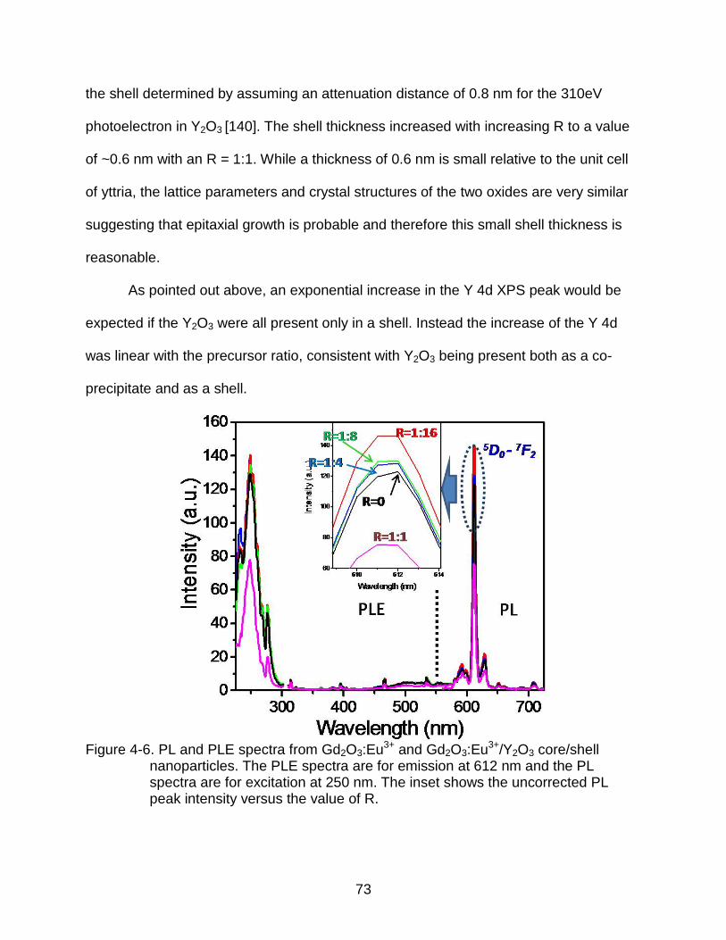
73
the shell determined by assuming an attenuation distance of 0.8 nm for the 310eV
photoelectron in Y2O3 [140]. The shell thickness increased with increasing R to a value
of ~0.6 nm with an R = 1:1. While a thickness of 0.6 nm is small relative to the unit cell
of yttria, the lattice parameters and crystal structures of the two oxides are very similar
suggesting that epitaxial growth is probable and therefore this small shell thickness is
reasonable.
As pointed out above, an exponential increase in the Y 4d XPS peak would be
expected if the Y2O3 were all present only in a shell. Instead the increase of the Y 4d
was linear with the precursor ratio, consistent with Y2O3 being present both as a co-
precipitate and as a shell.
Figure 4-6. PL and PLE spectra from Gd2O3:Eu3+ and Gd2O3:Eu3+/Y2O3 core/shell nanoparticles. The PLE spectra are for emission at 612 nm and the PL spectra are for excitation at 250 nm. The inset shows the uncorrected PL peak intensity versus the value of R.

74
The presence of both nanoparticles and shell Y2O3 is consistent with the
observation by TEM that the average particle size was constant and ~21 nm. A fraction
of the Y2O3 , must be present as nanoparticles based on the following argument.
Assuming that the shape of the core/shell nanoparticles is spherical and concentric
(Figure 4-5), and that the Gd and Y precursors react completely to produce only a core
and a shell, respectively, the Y2O3 shell would be ~2.3 nm thick for 21 nm diameter
cores and R = 1:1. This predicted shell thickness is four times larger than that measured
by XPS, leading to the conclusion that some of the Y2O3 exists as a separate phase,
consistent with the XRD peak shift in Figure 4-1c and Figure 4-2.
4.3.3 Photoluminescence Properties of Core and Core/Shell Nanoparticles
Figure 4-6 (a) shows PL and PLE spectra from the bare Gd2O3:Eu3+ and
Gd2O3:Eu3+/Y2O3 (core/shell) nanoparticles. PL emission and excitation spectra were
measured from thin films drop-cast as described above, and were very reproducible as
indicated by error bars in Figure 4-7. The PL spectra were dominated by the 5D0-7F2
transition of Eu3+ at 612 nm, while the PLE spectra were composed of a broad (FWHM
≈ 30 nm) peak centered at ~250 nm and sharp peaks between 360 and 530 nm. The
broad peak near 250 nm is from the oxygen to europium charge transfer band (CTB)
and the sharp peaks between 360 and 530 nm are from europium direct excitation. The
same characteristic PLE features have been reported for Eu3+-doped nanoparticles
prepared by combustion, precipitation and the polyol method using chloride precursors
[141-143]. All core/shell nanoparticles, except for the R = 1:1 sample, exhibited stronger
PL emission than did bare Gd2O3:Eu3+ nanoparticles. The PL intensity was measured
from a constant weight (volume) of nanoparticles, therefore it should have been lower at

75
all R values because a significant fraction of the sample was non-luminescent Y2O3
(due to the absence of Eu3+ dopants).
Without another effect such as surface passivation, weaker PL intensities would
be expected independent of whether the undoped Y2O3 was in a shell or in separate
nanoparticles The XRD data could also be consistent with forming a solid solution of
GdxY2-xO3:Eu3+ during calcining, but the temperature is too low for alloying. Furthermore,
Li, et al report lower PL from such a solution [144], which they attributed to less efficient
charge transfer between oxygen and yttrium versus oxygen to gadolinium.
Figure 4-7. Integrated area of PL peak at 612 nm versus R; Solid squares are uncorrected data. Solid diamonds are uncorrected normalized data. Open circles are normalized and corrected for the fraction of non-luminescent Y2O3 based on the value of R.
The enhanced PL shown by the corrected data in Figure 4-7 must result from
passivation due to formation of the core/shell structure. Figure 4-7 is a plot of integrated
area under the PL peak (560~725 nm and normalized to bare Gd2O3:Eu3+) versus the
76
Y2O3 shell thickness from the XPS data in Figure 4-4b. Without correcting for the
fraction of non-radiative Y2O3, the normalized PL intensity had an apparent maximum
(~1.2) at a shell thickness of 0.1 nm, grown with the lowest Y:Gd precursor ratio of
R=1:16. The normalized uncorrected PL intensity gradually decreased for higher values
of R (filled squares in Figure 4-7). However, after correcting for the fraction of non-
luminescent Y2O3 (open diamonds in Figure 4-7), all core/shell nanoparticles exhibit a
larger PL intensity than pure Gd2O3:Eu3+ nanoparticles, with the thickest shell of 0.6 nm
grown with the highest R=1:1 being ~40% brighter. This increased PL intensity is
attributed to a reduced concentration of non-radiative recombination surface sites due to
the Y2O3 shell on the Gd2O3:Eu3+ core. The larger increase in PL intensity at higher
precursor ratios is attributed to better passivation by the Y2O3 layer at larger values of R.
The quantum efficiency (QE) of the present Gd2O3/Y2O3 core/shell nanoparticles
was not measured, However, their QEs are expected to be ~40% based on our previous
results from similar materials [145].
4.3.4 Luminescence Decay Times of Core and Core/Shell Nanoparticles
To evaluate whether the rate of non-radiative decay was reduced by the formation
of the Y2O3 shell, the luminescence decay times were measured for bare Gd2O3:Eu3+
and Y2O3/Gd2O3:Eu3+ core/shell nanoparticles (Figure 4-8). The PL decay of both
unpassivated core (Figure 4-8a) and core/shell (Figure 4-8b with R = 1:1) nanoparticles
were very well fit by a single exponential function, i.e. by I=I0exp(-t/τ) where τ is the
decay time constant. As the thickness of the Y2O3 shell increased, the decay time (τ)
monotonically increased from 1.30 ms to 1.44 ms, as shown in Figure 4-8 (c). The
decay time for the 5D0 → 7F2 transition in Eu3+ doped Y2O3 or Gd2O3 has been reported
to be 1~2 ms [146, 147], consistent with our data. Even though the value of τ increased

77
only ~11% upon creation of the Y2O3 shell, the error bars in Figure 4-8 (c) are small,
indicating that the increase in decay time is real.
The longer luminescence decay time for Eu3+ in Gd2O3 is consistent with a reduced rate
of non-radiative relaxation due to the Y2O3 shell passivating surface states [87, 148].
Figure 4-8. Luminescence decay data for the Eu3+ 5D0-7F2 transition (612 nm peak). The data are well fit by the solid line which is a single exponential function with a time constant
Unpassivated surface states are known to trap charge carriers which lead to fast non-
radiative recombination and therefore shorter luminescent relaxation time constants.
78
4.4 Conclusion
Nanocores (~21 nm diameter) of Gd2O3:Eu3+ with both a Y2O3 shell and undoped
Y2O3 co-precipitated nanoparticles were synthesized by a facile two-step high boiling-
point alcohol (polyol) method at 180 °C in air for times of a few hours. Data from XRD,
TEM, XPS, PL and luminescent decay time measurements from calcined (600 °C, 2 hrs
in air) samples showed that crystalline Y2O3 shells up to 0.6 nm thick were formed on
the crystalline Gd2O3:Eu3+ core and that the thickest shell resulted in a 40% increase in
PL intensity and an 11% longer PL decay time relative to uncoated Gd2O3:Eu3+
nanoparticles. These changes were attributed to passivation of surface states that
resulted in reduced rates of non-radiative relaxation processes.
79
CHAPTER 5 ENHANCED PHOTOLUMINESCENCE FROM EUROPIUM DOPED GADOLINIUM
OXIDE BASED CORE/DUAL-SHELL NANOPARTICLES
5.1 Introduction
Nanophosphors with rare-earth materials are of interest due to their potential
applications in lightings, displays, biological diagnosis and scintillators [125, 145, 149,
150]. Among rare-earth materials, gadolinium oxide is a versatile material with potential
applications in several fields of technology. When doped with rare-earth ions (Eu3+ and
Tb3+), it exhibits good luminescent properties [47, 151, 152].
For nanophosphors, core/shell hetero-structures have been created in two
different configurations, the first of which is a luminescent core and surface passivation
shell. Several investigators have reported that the luminescent efficiency of
nanophosphors was lower than that of their corresponding bulk counterparts due to the
non-radiative recombination at surface defects [87, 131]. They frequently reported
increased luminescent efficiency upon addition of the passivating shell [122, 123]. A
second configuration of the core/shell hetero-structure is a non-luminescent core and
luminescent shell. There are several reports of silica nanocores coated with various
phosphor shells [132, 153, 154]. These core/shell structures have several advantages,
the first being easy control of the size of mono-dispersed spherical silica cores from
nanometers to micrometers [155, 156]. Second, silica is cheap as compared to the
more expensive rare earth phosphor materials, therefore the silica core/luminescent
shell structures should result in lower costs. However, luminescent shells inherently
have very large surface to volume ratio, and frequently exhibit low quantum yields due
to surface states. Here we report a silica core/dual-shell with a luminescent Gd2O3:Eu3+

80
shell and passivating Y2O3 shell which can reduce cost and double the quantum yield
these potential scintillator materials.
5.2 Experimental
5.2.1 Materials
Gd(III) nitrate hydrate (99.9%), Eu(III) nitrate hexahydrate (99.9%) and Y(III)
nitrate (99.9%) were purchased from Aldrich Chemical Co.. Tetraethyl orthosilicate
(TEOS, 98%) and ethanol were purchased from Acros Organics. All chemicals were
analytical grade and were used without further purification.
5.2.2 Synthesis of Silica Cores
Silica nanocores were fabricated via the Stöber method [157], where 5 ml of
concentrated ammonium hydroxide (NH4OH) was mixed with 20 ml of deionized (DI)
water and 100 ml of ethanol and stirred vigorously. Then 10 ml of tetraethyl orthosilicate
(TEOS) was added quickly and stirred for 2 hrs without heating. After a few minutes, the
solution became translucent and then cloudy white as the SiO2 particles grew large
enough to scatter visible light. To remove unreacted precursors, the nanoparticles were
centrifuged and re-dispersed in ethanol at least three times, followed by drying at 70 °C
for 12 hrs in air.
5.2.3 Synthesis of Gd2O3:Eu3+ Shell on SiO2 Cores
Growth of Gd1.6O3:Eu0.43+ shells was accomplished with a solution precipitation
method, in which 500 mg of silica cores were added to 100 ml of DI water and the
mixture was sonicated to achieve a homogeneous suspension. This was followed by
addition of 4 mmol of gadolinium nitrate and 1 mmol of europium nitrate and 125 mmol
of urea which was reacted at 85 °C. After 1.5 hrs synthesis, nanoparticles were
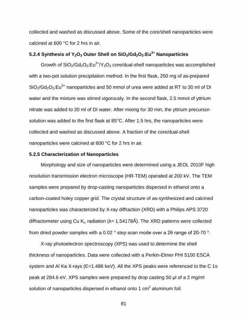
81
collected and washed as discussed above. Some of the core/shell nanoparticles were
calcined at 600 °C for 2 hrs in air.
5.2.4 Synthesis of Y2O3 Outer Shell on SiO2/Gd2O3:Eu3+ Nanoparticles
Growth of SiO2/Gd2O3:Eu3+/Y2O3 core/dual-shell nanoparticles was accomplished
with a two-pot solution precipitation method. In the first flask, 250 mg of as-prepared
SiO2/Gd2O3:Eu3+ nanoparticles and 50 mmol of urea were added at RT to 30 ml of DI
water and the mixture was stirred vigorously. In the second flask, 2.5 mmol of yttrium
nitrate was added to 20 ml of DI water. After mixing for 30 min, the yttrium precursor-
solution was added to the first flask at 85°C. After 1.5 hrs, the nanoparticles were
collected and washed as discussed above. A fraction of the core/dual-shell
nanoparticles were calcined at 600 °C for 2 hrs in air.
5.2.5 Characterization of Nanoparticles
Morphology and size of nanoparticles were determined using a JEOL 2010F high
resolution transmission electron microscope (HR-TEM) operated at 200 kV. The TEM
samples were prepared by drop-casting nanoparticles dispersed in ethanol onto a
carbon-coated holey copper grid. The crystal structure of as-synthesized and calcined
nanoparticles was characterized by X-ray diffraction (XRD) with a Philips APS 3720
diffractometer using Cu Kα radiation (λ= 1.54178Å). The XRD patterns were collected
from dried powder samples with a 0.02 ° step scan mode over a 2θ range of 20-70 °.
X-ray photoelectron spectroscopy (XPS) was used to determine the shell
thickness of nanoparticles. Data were collected with a Perkin-Elmer PHI 5100 ESCA
system and Al Ka X-rays (E=1.486 keV). All the XPS peaks were referenced to the C 1s
peak at 284.6 eV. XPS samples were prepared by drop casting 50 μl of a 2 mg/ml
solution of nanoparticles dispersed in ethanol onto 1 cm2 aluminum foil.

82
Photoluminescence (PL), photoluminescence excitation (PLE) spectra and luminescent
relaxation lifetime were measured at room temperature using a JASCO FP-6500/6600
research grade fluorescence spectrometer with a 150 W Xenon lamp. Quantum yields
were measured using an integrating sphere. The samples for PL, PLE and quantum
yields were films prepared by adding calcined nanoparticles to 500 μL of 4% of
poly(methyl methacrylate) (PMMA) dispersed in chlorobenzene and drop-cast onto
quartz substrates.
5.3 Results and Discussion
5.3.1 Morphology and Crystal Structure of Core/Shell Nanoparticles
The morphology and size of as-prepared SiO2 nanocores are shown in Figure 5-
1(a). Based on TEM images, mono-dispersed SiO2 nanocores were spherical and with
a diameter of 450 nm. A ~5 nm of Gd2O3:Eu3+ layer was coated on SiO2 nanocores by
the urea precipitation method, as shown in Figure 5-1(b and c). A nearly uniform
SiO2/Gd2O3:Eu3+ core/shell nanostructure was obtained, as indicated by the outer
darker and inner lighter regions corresponding to the Gd2O3:Eu3+ shell and SiO2 core,
respectively. Figure 5-1(d) shows a SiO2/Gd2O3:Eu3+/Y2O3 core/dual-shell nanoparticle.
A dark Gd2O3:Eu3+ ring between two lighter regions is observed, due to differences in
the average atomic number. The outer Y2O3 shell is ∼45 nm thick and it uniformly
covers the SiO2/Gd2O3:Eu3+ core/single-shell nanoparticles. According to XRD data, as-
grown silica nanocores were amorphous with an amorphous scattering peak at ~27 o,
as shown in Figure 5-2(a). However, calcined SiO2/Gd2O3:Eu3+ core/shell nanoparticles
showed crystalline peaks that matched JCPDS data from cubic Gd2O3 (Card 43-1014).
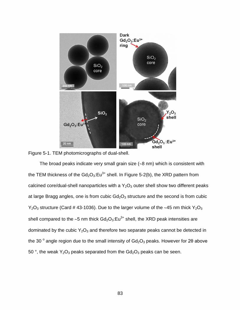
83
Figure 5-1. TEM photomicrographs of dual-shell.
The broad peaks indicate very small grain size (∼8 nm) which is consistent with
the TEM thickness of the Gd2O3:Eu3+ shell. In Figure 5-2(b), the XRD pattern from
calcined core/dual-shell nanoparticles with a Y2O3 outer shell show two different peaks
at large Bragg angles, one is from cubic Gd2O3 structure and the second is from cubic
Y2O3 structure (Card # 43-1036). Due to the larger volume of the ∼45 nm thick Y2O3
shell compared to the ∼5 nm thick Gd2O3:Eu3+ shell, the XRD peak intensities are
dominated by the cubic Y2O3 and therefore two separate peaks cannot be detected in
the 30 o angle region due to the small intensity of Gd2O3 peaks. However for 2θ above
50 °, the weak Y2O3 peaks separated from the Gd2O3 peaks can be seen.

84
Figure 5-2. X-Ray diffraction spectra obtained from pure amorphous silica nanoparticles or calcined SiO2/Gd2O3:Eu3+ core/single-shell nanoparticles and calcined SiO2/Gd2O3:Eu3+/Y2O3 core/dual-shell nanoparticles.
5.3.2 Surface Analysis of Core/Shell Nanoparticles
X-ray photoelectron spectroscopy (XPS) analysis is commonly used to investigate
the composition and chemical bonds in surface layers up to depths of a few nm. If SiO2
nanocores are coated with Gd2O3:Eu3+ and Y2O3 shells, the XPS signal from the core
should be much less than those from the shells. Figure 5-3 shows XPS data for binding
energies between 135-170 eV from films of SiO2 core, SiO2/Gd2O3:Eu3+ core/single-
shell and SiO2/Gd2O3:Eu3+/Y2O3 core/dual-shell nanoparticles. For a SiO2 nanocore
sample, only the Si 2s peak (binding energy (BE) ~157 eV) was detected. A core/dual-
shell sample with a thick Y2O3 outer shell exhibited only the Y 3d peak (BE ∼ 163 eV).
However, a core/single-shell sample with an ∼5 nm Gd2O3:Eu3+ layers showed a small
Si 2s peak at BE ~ 157 eV, as well as a large Gd 4d peaks (BE ~ 147 eV). The small
157 eV Si 2s XPS peak results from an exponential attenuation of the intensity of the
silica core photoelectron peak [139].

85
Figure 5-3. X-ray photoelectron peaks from the SiO2 nanocores (solid line), from SiO2/Gd2O3:Eu3+ core/single-shell (dashed line) and SiO2/Gd2O3:Eu3+/Y2O3 core/dual-shell nanoparticles (dotted line).
Figure 5-4. The Si 2p XPS peaks from SiO2, SiO2/Gd2O3:Eu3+ core/single-shell nanoparticles and normalized intensity of the Si 2p peak versus Gd2O3:Eu3+ shell thickness.
To avoid ambiguity due to overlap with other peaks, attenuation of the Si 2p XPS
peak (BE ~ 106 eV) was analyzed, as shown in Figure 5-4(a). Since attenuation of XPS
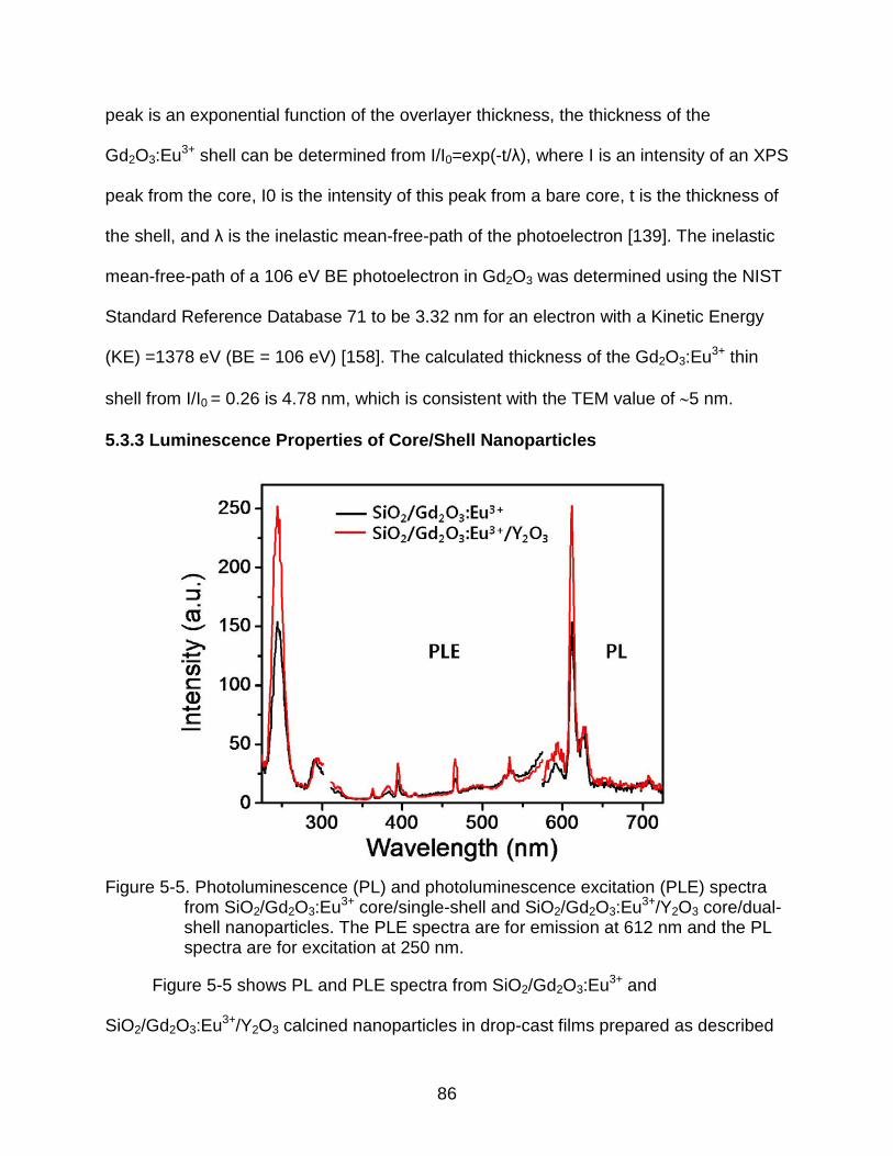
86
peak is an exponential function of the overlayer thickness, the thickness of the
Gd2O3:Eu3+ shell can be determined from I/I0=exp(-t/λ), where I is an intensity of an XPS
peak from the core, I0 is the intensity of this peak from a bare core, t is the thickness of
the shell, and λ is the inelastic mean-free-path of the photoelectron [139]. The inelastic
mean-free-path of a 106 eV BE photoelectron in Gd2O3 was determined using the NIST
Standard Reference Database 71 to be 3.32 nm for an electron with a Kinetic Energy
(KE) =1378 eV (BE = 106 eV) [158]. The calculated thickness of the Gd2O3:Eu3+ thin
shell from I/I0 = 0.26 is 4.78 nm, which is consistent with the TEM value of ∼5 nm.
5.3.3 Luminescence Properties of Core/Shell Nanoparticles
Figure 5-5. Photoluminescence (PL) and photoluminescence excitation (PLE) spectra from SiO2/Gd2O3:Eu3+ core/single-shell and SiO2/Gd2O3:Eu3+/Y2O3 core/dual-shell nanoparticles. The PLE spectra are for emission at 612 nm and the PL spectra are for excitation at 250 nm.
Figure 5-5 shows PL and PLE spectra from SiO2/Gd2O3:Eu3+ and
SiO2/Gd2O3:Eu3+/Y2O3 calcined nanoparticles in drop-cast films prepared as described
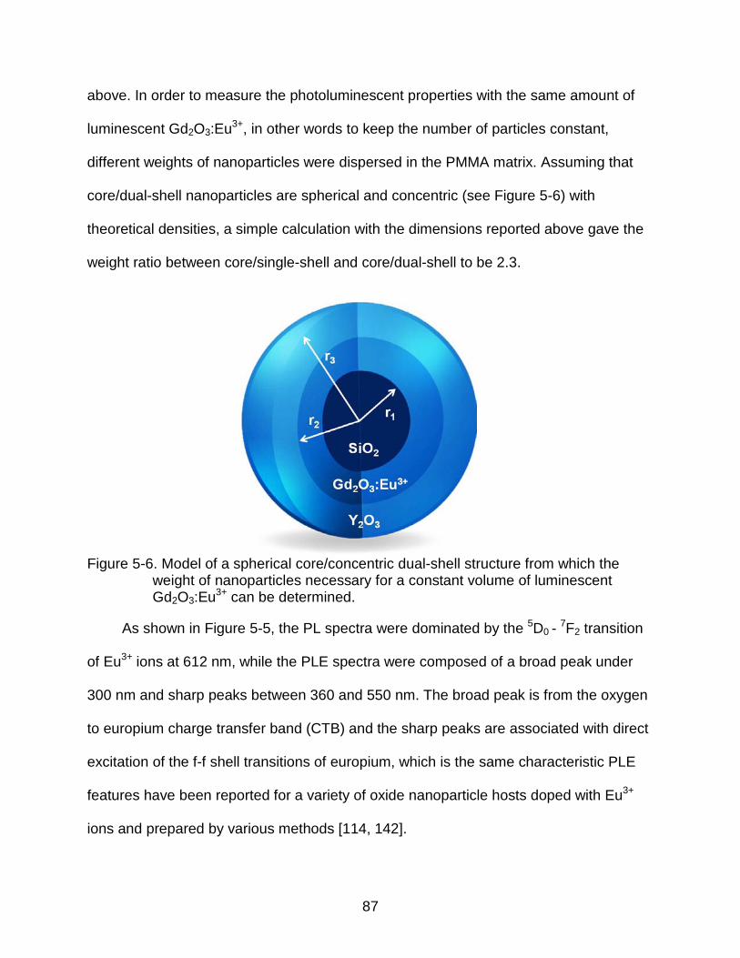
87
above. In order to measure the photoluminescent properties with the same amount of
luminescent Gd2O3:Eu3+, in other words to keep the number of particles constant,
different weights of nanoparticles were dispersed in the PMMA matrix. Assuming that
core/dual-shell nanoparticles are spherical and concentric (see Figure 5-6) with
theoretical densities, a simple calculation with the dimensions reported above gave the
weight ratio between core/single-shell and core/dual-shell to be 2.3.
Figure 5-6. Model of a spherical core/concentric dual-shell structure from which the weight of nanoparticles necessary for a constant volume of luminescent Gd2O3:Eu3+ can be determined.
As shown in Figure 5-5, the PL spectra were dominated by the 5D0 - 7F2 transition
of Eu3+ ions at 612 nm, while the PLE spectra were composed of a broad peak under
300 nm and sharp peaks between 360 and 550 nm. The broad peak is from the oxygen
to europium charge transfer band (CTB) and the sharp peaks are associated with direct
excitation of the f-f shell transitions of europium, which is the same characteristic PLE
features have been reported for a variety of oxide nanoparticle hosts doped with Eu3+
ions and prepared by various methods [114, 142].
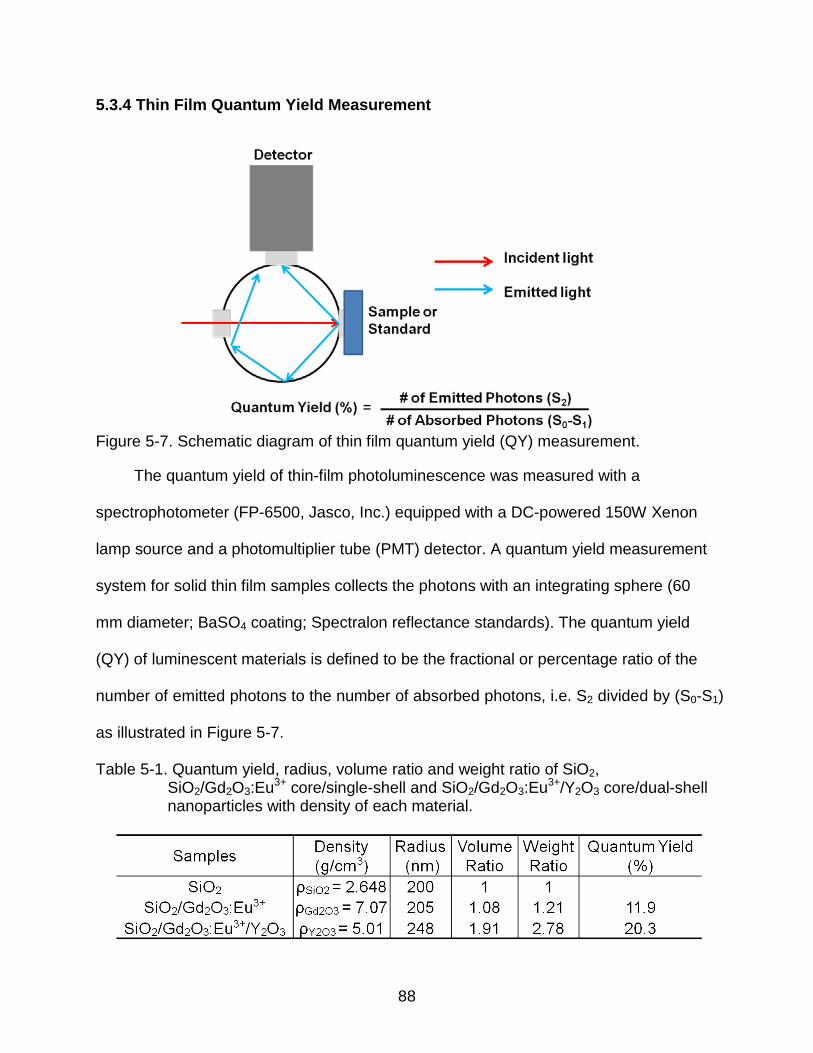
88
5.3.4 Thin Film Quantum Yield Measurement
Figure 5-7. Schematic diagram of thin film quantum yield (QY) measurement.
The quantum yield of thin-film photoluminescence was measured with a
spectrophotometer (FP-6500, Jasco, Inc.) equipped with a DC-powered 150W Xenon
lamp source and a photomultiplier tube (PMT) detector. A quantum yield measurement
system for solid thin film samples collects the photons with an integrating sphere (60
mm diameter; BaSO4 coating; Spectralon reflectance standards). The quantum yield
(QY) of luminescent materials is defined to be the fractional or percentage ratio of the
number of emitted photons to the number of absorbed photons, i.e. S2 divided by (S0-S1)
as illustrated in Figure 5-7.
Table 5-1. Quantum yield, radius, volume ratio and weight ratio of SiO2, SiO2/Gd2O3:Eu3+ core/single-shell and SiO2/Gd2O3:Eu3+/Y2O3 core/dual-shell nanoparticles with density of each material.
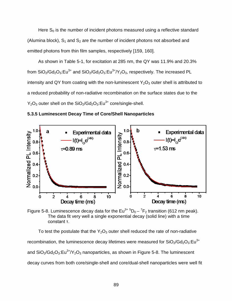
89
Here S0 is the number of incident photons measured using a reflective standard
(Alumina block), S1 and S2 are the number of incident photons not absorbed and
emitted photons from thin film samples, respectively [159, 160].
As shown in Table 5-1, for excitation at 285 nm, the QY was 11.9% and 20.3%
from SiO2/Gd2O3:Eu3+ and SiO2/Gd2O3:Eu3+/Y2O3, respectively. The increased PL
intensity and QY from coating with the non-luminescent Y2O3 outer shell is attributed to
a reduced probability of non-radiative recombination on the surface states due to the
Y2O3 outer shell on the SiO2/Gd2O3:Eu3+ core/single-shell.
5.3.5 Luminescent Decay Time of Core/Shell Nanoparticles
Figure 5-8. Luminescence decay data for the Eu3+ 5D0 – 7F2 transition (612 nm peak). The data fit very well a single exponential decay (solid line) with a time constant τ.
To test the postulate that the Y2O3 outer shell reduced the rate of non-radiative
recombination, the luminescence decay lifetimes were measured for SiO2/Gd2O3:Eu3+
and SiO2/Gd2O3:Eu3+/Y2O3 nanoparticles, as shown in Figure 5-8. The luminescent
decay curves from both core/single-shell and core/dual-shell nanoparticles were well fit

90
by a single exponential curve, i.e. by I=I0exp(-t/τ), where τ is the decay time constant.
The Y2O3 outer shell on SiO2/Gd2O3:Eu3+ core/single-shell nanoparticles increased the
decay times from 0.89 ms to 1.53 ms, consistent with a sharp reduction in non-radiative
transitions, and therefore more radiative relaxation over longer time constants.
The decay time for the 5D0 - 7F2 transition in Eu3+ doped rare-earth oxides has
reported to be ∼1-2 ms [147, 161]. The short decay time of core/single-shell
nanoparticles of 0.89 ms can we explain by the fact that the SiO2/Gd2O3:Eu3+ core/shell
nanoparticles are spherical and concentric, as described above, therefore the
percentage of atoms locating on the outer surface (presumably was unsatisfied bonding)
is approximately over 25%. Because of the dangling chemical bonds, there apparently
were a large density of surface defects that trapped charge carriers and led to fast non-
radiative recombination and therefore shorter luminescent relaxation time constants [87].
The Y2O3 outer shell reduced the density of surface states and led to longer relaxation
times.
5.4 Conclusion
Nanocores (400 nm diameter) of SiO2 with a 4.5 nm thick Gd2O3:Eu3+ shell, and
sometimes with a 43 nm thick Y2O3 shell, were synthesized by the Stöber and by
solution precipitation methods. The nanostructures were characterized by XRD, TEM,
XPS and PL. As-synthesized samples were amorphous, but the shells after calcination
(600 °C, 2 h in air) were crystalline, with both Gd2O3:Eu3+ and Y2O3 shells being cubic
while the SiO2 core remained amorphous. Excitation in the UV led to emission at ∼612
nm from the Eu3+ dopant in the Gd2O3 shell with a quantum yield of 12%. Addition of the
Y2O3 shell increased the PL intensity by 72%, raising the QY to 20%. The increased QY

91
was attributed to passivation of surface states that led to reduced surface defect density
and lower rate of non-radiative relaxation.
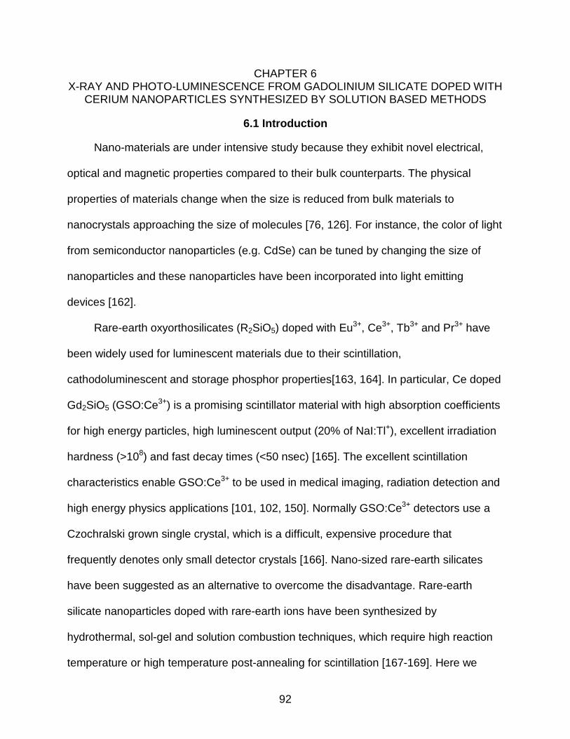
92
CHAPTER 6 X-RAY AND PHOTO-LUMINESCENCE FROM GADOLINIUM SILICATE DOPED WITH
CERIUM NANOPARTICLES SYNTHESIZED BY SOLUTION BASED METHODS
6.1 Introduction
Nano-materials are under intensive study because they exhibit novel electrical,
optical and magnetic properties compared to their bulk counterparts. The physical
properties of materials change when the size is reduced from bulk materials to
nanocrystals approaching the size of molecules [76, 126]. For instance, the color of light
from semiconductor nanoparticles (e.g. CdSe) can be tuned by changing the size of
nanoparticles and these nanoparticles have been incorporated into light emitting
devices [162].
Rare-earth oxyorthosilicates (R2SiO5) doped with Eu3+, Ce3+, Tb3+ and Pr3+ have
been widely used for luminescent materials due to their scintillation,
cathodoluminescent and storage phosphor properties[163, 164]. In particular, Ce doped
Gd2SiO5 (GSO:Ce3+) is a promising scintillator material with high absorption coefficients
for high energy particles, high luminescent output (20% of NaI:Tl+), excellent irradiation
hardness (>108) and fast decay times (<50 nsec) [165]. The excellent scintillation
characteristics enable GSO:Ce3+ to be used in medical imaging, radiation detection and
high energy physics applications [101, 102, 150]. Normally GSO:Ce3+ detectors use a
Czochralski grown single crystal, which is a difficult, expensive procedure that
frequently denotes only small detector crystals [166]. Nano-sized rare-earth silicates
have been suggested as an alternative to overcome the disadvantage. Rare-earth
silicate nanoparticles doped with rare-earth ions have been synthesized by
hydrothermal, sol-gel and solution combustion techniques, which require high reaction
temperature or high temperature post-annealing for scintillation [167-169]. Here we
93
report a non-hydrolytic colloidal hot-solution growth method to produce nanocrystals of
GSO. Colloidal growth in non-hydrolytic liquid media can produce a variety of shapes
and 1–10 nm sizes of highly crystallized nanocrystals that can be dispersed in organic
or aqueous media for numerous potential applications [25]. This chapter describes the
synthesis of GSO:Ce3+ nanoparticles and their structural characteristics and
photoluminescence properties by UV and X-ray excitations.
6.2 Experimental
6.2.1 Hot Solution Synthesis
Gd2SiO5 doped with Ce3+ (Ce3+ = 0.1, 0.2, 0.5, 2 and 5 mol %) nanoparticles were
prepared by a two-pot hot solution synthesis for 90 min in oleylamine (Figure 6-1). The
doping concentration is corresponding to the molar concentration of precursors. In a
typical reaction to produce GSO nanoparticles doped with 5 mol % Ce3+, 1.9 mmol of
Gd acetate was mixed with 5 ml of oleylamine in a three-neck reaction flask and heated
to 120 °C. At the same time, 0.1 mmol of Ce acetate was mixed with 2 ml of oleylamine
in a vial and heated to 120 °C. After 30 min, the Ce precursor solution was mixed with
the Gd precursor solution and 2 mmol of (3-Aminopropyl)triethoxysilane (APTES) was
injected into the precursor mixture solution. Finally, the temperature was raised to ~
320 °C with a heating rate of 5-25 °C/min and maintained at that temperature for 90 min
with vigorous stirring. After reflux, the brownish mixture was cooled down to room
temperature by removing the heat source. Ethanol was added to the mixture, and
GSO:Ce3+ nanoparticles were precipitated and separated by centrifugations. This
procedure was repeated at least three times to remove any residue. The purified
GSO:Ce3+ nanoparticles, capped with organic species, were well dispersed by organic
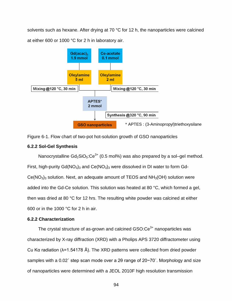
94
solvents such as hexane. After drying at 70 °C for 12 h, the nanoparticles were calcined
at either 600 or 1000 °C for 2 h in laboratory air.
Figure 6-1. Flow chart of two-pot hot-solution growth of GSO nanoparticles
6.2.2 Sol-Gel Synthesis
Nanocrystalline Gd2SiO5:Ce3+ (0.5 mol%) was also prepared by a sol–gel method.
First, high-purity Gd(NO3)3 and Ce(NO3)3 were dissolved in DI water to form Gd-
Ce(NO3)3 solution. Next, an adequate amount of TEOS and NH3(OH) solution were
added into the Gd-Ce solution. This solution was heated at 80 °C, which formed a gel,
then was dried at 80 °C for 12 hrs. The resulting white powder was calcined at either
600 or in the 1000 °C for 2 h in air.
6.2.2 Characterization
The crystal structure of as-grown and calcined GSO:Ce3+ nanoparticles was
characterized by X-ray diffraction (XRD) with a Pholips APS 3720 diffractometer using
Cu Kα radiation (λ=1.54178 Å). The XRD patterns were collected from dried powder
samples with a 0.02˚ step scan mode over a 2θ range of 20~70˚. Morphology and size
of nanoparticles were determined with a JEOL 2010F high resolution transmission
* APTES : (3-Aminopropyl)triethoxysilane
95
electron microscope (HR-TEM) operated at an accelerating voltage of 200 kV.
Specimens for the TEM were prepared by drop-casting particles dispersed in ethanol
onto holey carbon-coated copper grids. Photoluminescence (PL) and
photoluminescence excitation (PLE) spectra were measured at room temperature using
a JASCO FP-6500/6600 research grade fluorescence spectrometer with a 150 W
Xenon lamp. X-ray luminescence was measured with a 40 kV BulletTM X-ray tube
combined with a Ocean Optics USB-2000 miniature fiber optic spectrometer. The
distance from the x-ray target to the sample was ~3 cm and the x-ray tube was operated
at 100 μA. For each measurement, a crucible with 57 mm2 area was filled with
nanopowder such that each sample had the same area exposed to the x-rays.
Differential pulse height distribution measurements was obtained by a Hidex Triathler®
scintillation counter with a Hamamatsu R850-photomultiplier tube and a 1 μCi 241Am (E
= 60 keV) source. The Trialther® was configured with logarithmic amplification to
accentuate the difference in the differential pulse height spectra. In our measurements,
the relative positions of the samples, detector and source were kept fixed, with the
plated 241Am source being suspended ~1 cm above power contained in a 3.7 ml glass
vial. The electronic noise background was determined by measuring an empty vial in
identical conditions as the nanopowder sample.
6.3 Results and Discussion
6.3.1 Thermogravimetric Analysis (TGA) of GSO Nanoparticles
Nanoparticles grown by the hot-solution growth (HSG) method were covered by
the organic solvent, which often reduces the photoluminescence brightness. Calcining
the GSO:Ce3+ nanoparticles at a sufficiently high temperature will remove the
oleylamine, based on thermogravimetric analysis (TGA).
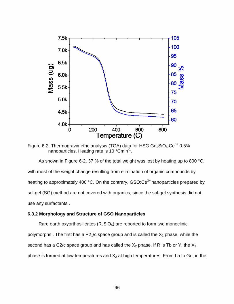
96
Figure 6-2. Thermogravimetric analysis (TGA) data for HSG Gd2SiO5:Ce3+ 0.5% nanoparticles. Heating rate is 10 °Cmin-1.
As shown in Figure 6-2, 37 % of the total weight was lost by heating up to 800 °C,
with most of the weight change resulting from elimination of organic compounds by
heating to approximately 400 °C. On the contrary, GSO:Ce3+ nanoparticles prepared by
sol-gel (SG) method are not covered with organics, since the sol-gel synthesis did not
use any surfactants .
6.3.2 Morphology and Structure of GSO Nanoparticles
Rare earth oxyorthosilicates (R2SiO5) are reported to form two monoclinic
polymorphs . The first has a P21/c space group and is called the X1 phase, while the
second has a C2/c space group and has called the X2 phase. If R is Tb or Y, the X1
phase is formed at low temperatures and X2 at high temperatures. From La to Gd, in the

97
order of the periodic table, the X1 phase is formed, whereas Dy to Lu forms the X2
phase [170].
Figure 6-3. XRD patterns from Gd2SiO5:Ce3+ nanoparticles compared to the JCDPS pattern for monoclinic Gd2SiO5 (JCPDS # : 40-0282) : GSO:Ce3+ nanoparticles after calcination at 600 °C and 1000 °C for 2hr in air.
In the present study, as-synthesized nanoparticles were amorphous with the
typical broad XRD amorphous peak at ∼27o. Despite of calcination at 600 °C,
GSO:Ce3+ nanoparticles from both HSG and SG remained amorphous, as shown by
XRD data in Figure 6-3 (a). In contrast, the XRD spectra from both HSG and SG
GSO:Ce3+ nanoparticles calcined at 1000 °C for 2hr were crystalline with peaks that
match the JCPDS data for X1 monoclinic Gd2SiO5 (Card 40-0287). Using the Scherrer
equation, broadening of the (321) peak for both synthesis methods indicated an
average nanoparticle diameter of 40-50 nm.
Figure 6-4 shows HR-TEM and Selected Area Diffraction (SAD) images of sol-gel
prepared GSO:Ce3+ nanoparticles (a and b) and hot-solution prepared GSO:Ce3+
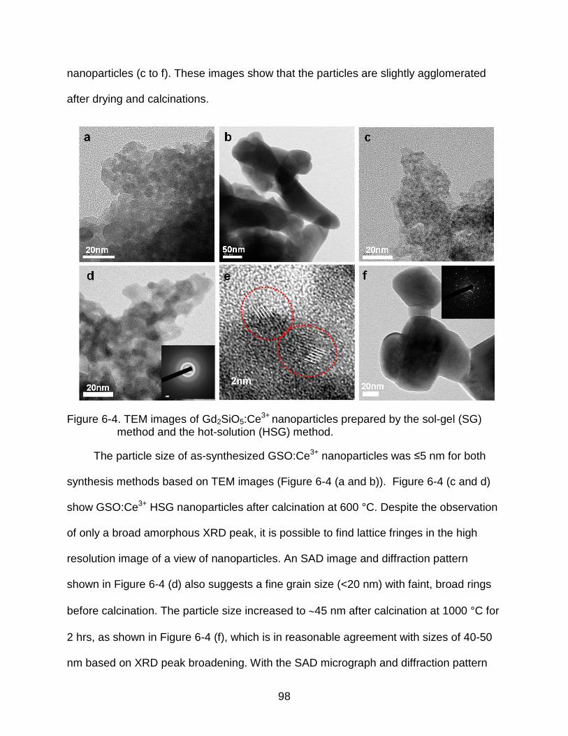
98
nanoparticles (c to f). These images show that the particles are slightly agglomerated
after drying and calcinations.
Figure 6-4. TEM images of Gd2SiO5:Ce3+ nanoparticles prepared by the sol-gel (SG) method and the hot-solution (HSG) method.
The particle size of as-synthesized GSO:Ce3+ nanoparticles was ≤5 nm for both
synthesis methods based on TEM images (Figure 6-4 (a and b)). Figure 6-4 (c and d)
show GSO:Ce3+ HSG nanoparticles after calcination at 600 °C. Despite the observation
of only a broad amorphous XRD peak, it is possible to find lattice fringes in the high
resolution image of a view of nanoparticles. An SAD image and diffraction pattern
shown in Figure 6-4 (d) also suggests a fine grain size (<20 nm) with faint, broad rings
before calcination. The particle size increased to ∼45 nm after calcination at 1000 °C for
2 hrs, as shown in Figure 6-4 (f), which is in reasonable agreement with sizes of 40-50
nm based on XRD peak broadening. With the SAD micrograph and diffraction pattern

99
inset of Figure 6-4 (f), incomplete ring patterns indicate larger crystalline grains after
calcining at 1000 °C, consistent with the XRD data in Figure 6-3.
6.3.3 Luminescent Properties of GSO Nanoparticles
Figure 6-5. PL spectra and intensity for various Ce concentrations showing quenching for Gd2SiO5:Ce3+ nanoparticles synthesized by the hot-solution method (excitation wavelength = 344 nm).
It is well known that the optimum dopant concentration in a phosphor depends on
both the host and rare-earth dopants. For nanophosphors, concentration quenching
behavior of photoluminescence has been reported for YSO:Eu3+ [171] and Gd2O3:Eu3+
[122], and the general trend is that the optimum dopant concentration in nanophosphors
is much higher than for the bulk materials.
As shown in Figure 5, GSO:Ce3+ nanoparticles prepared by HSG exhibited the
highest PL intensity for 0.5% Ce, which is higher than that of bulk oxyorthosilicates
grown by the CZ method in which the optimum concentration is generally ≤0.05% [172].
Figure 6-6 shows photoluminescence emission (PL) and photoluminescence excitation
(PLE) spectra from calcined GSO:Ce3+ nanoparticles prepared by the (a) hot-solution
and (b) sol-gel methods, respectively. PL emission and excitation spectra were
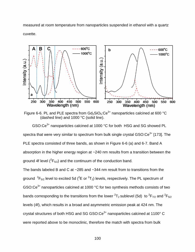
100
measured at room temperature from nanoparticles suspended in ethanol with a quartz
cuvette.
Figure 6-6. PL and PLE spectra from Gd2SiO5:Ce3+ nanoparticles calcined at 600 °C (dashed line) and 1000 °C (solid line).
GSO:Ce3+ nanoparticles calcined at 1000 °C for both HSG and SG showed PL
spectra that were very similar to spectrum from bulk single crystal GSO:Ce3+ [173]. The
PLE spectra consisted of three bands, as shown in Figure 6-6 (a) and 6-7. Band A
absorption in the higher energy region at ~240 nm results from a transition between the
ground 4f level (2F5/2) and the continuum of the conduction band.
The bands labeled B and C at ~285 and ~344 nm result from to transitions from the
ground 2F5/2 level to excited 5d (2E or 2T2) levels, respectively. The PL spectrum of
GSO:Ce3+ nanoparticles calcined at 1000 °C for two synthesis methods consists of two
bands corresponding to the transitions from the lower 2T2 sublevel (5d) to 2F7/2 and 2F5/2
levels (4f), which results in a broad and asymmetric emission peak at 424 nm. The
crystal structures of both HSG and SG GSO:Ce3+ nanoparticles calcined at 1100° C
were reported above to be monoclinic, therefore the match with spectra from bulk
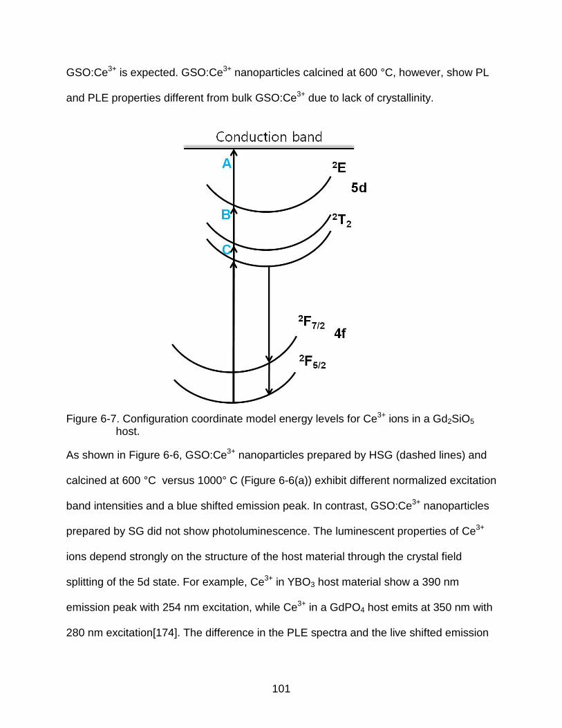
101
GSO:Ce3+ is expected. GSO:Ce3+ nanoparticles calcined at 600 °C, however, show PL
and PLE properties different from bulk GSO:Ce3+ due to lack of crystallinity.
Figure 6-7. Configuration coordinate model energy levels for Ce3+ ions in a Gd2SiO5 host.
As shown in Figure 6-6, GSO:Ce3+ nanoparticles prepared by HSG (dashed lines) and
calcined at 600 °C versus 1000° C (Figure 6-6(a)) exhibit different normalized excitation
band intensities and a blue shifted emission peak. In contrast, GSO:Ce3+ nanoparticles
prepared by SG did not show photoluminescence. The luminescent properties of Ce3+
ions depend strongly on the structure of the host material through the crystal field
splitting of the 5d state. For example, Ce3+ in YBO3 host material show a 390 nm
emission peak with 254 nm excitation, while Ce3+ in a GdPO4 host emits at 350 nm with
280 nm excitation[174]. The difference in the PLE spectra and the live shifted emission
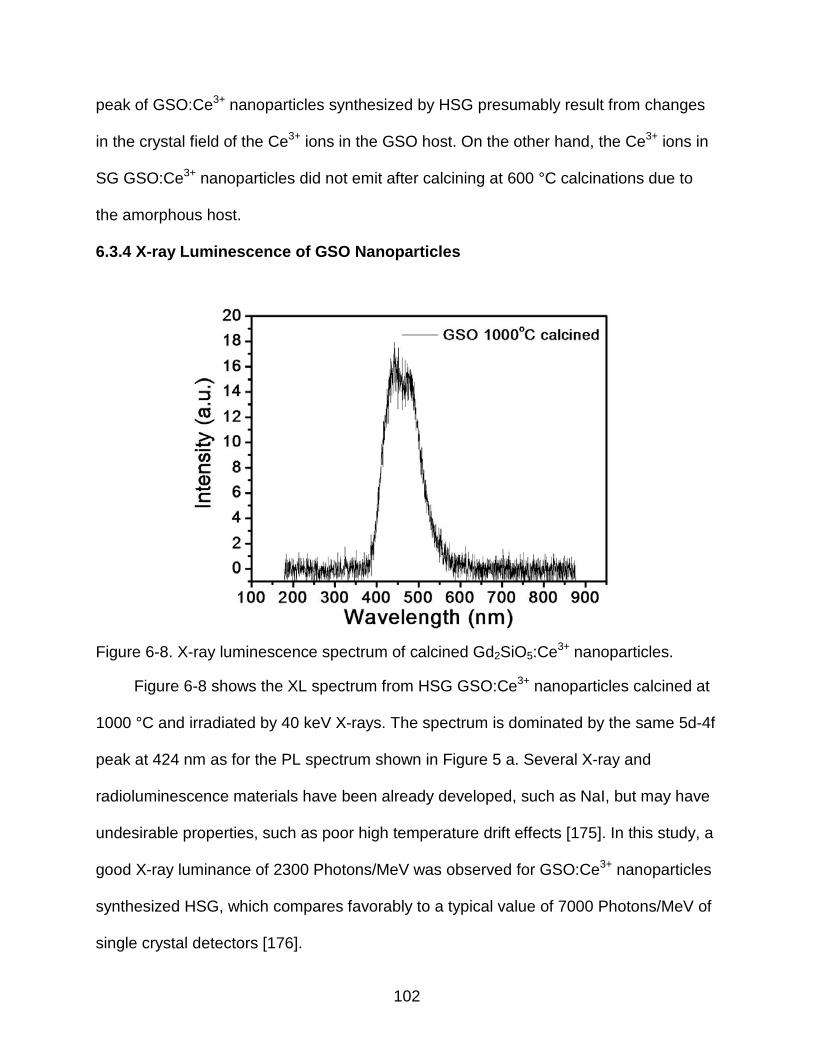
102
peak of GSO:Ce3+ nanoparticles synthesized by HSG presumably result from changes
in the crystal field of the Ce3+ ions in the GSO host. On the other hand, the Ce3+ ions in
SG GSO:Ce3+ nanoparticles did not emit after calcining at 600 °C calcinations due to
the amorphous host.
6.3.4 X-ray Luminescence of GSO Nanoparticles
Figure 6-8. X-ray luminescence spectrum of calcined Gd2SiO5:Ce3+ nanoparticles.
Figure 6-8 shows the XL spectrum from HSG GSO:Ce3+ nanoparticles calcined at
1000 °C and irradiated by 40 keV X-rays. The spectrum is dominated by the same 5d-4f
peak at 424 nm as for the PL spectrum shown in Figure 5 a. Several X-ray and
radioluminescence materials have been already developed, such as NaI, but may have
undesirable properties, such as poor high temperature drift effects [175]. In this study, a
good X-ray luminance of 2300 Photons/MeV was observed for GSO:Ce3+ nanoparticles
synthesized HSG, which compares favorably to a typical value of 7000 Photons/MeV of
single crystal detectors [176].
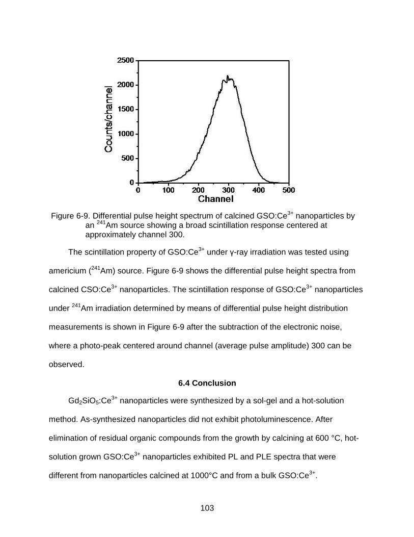
103
Figure 6-9. Differential pulse height spectrum of calcined GSO:Ce3+ nanoparticles by an 241Am source showing a broad scintillation response centered at approximately channel 300.
The scintillation property of GSO:Ce3+ under γ-ray irradiation was tested using
americium (241Am) source. Figure 6-9 shows the differential pulse height spectra from
calcined CSO:Ce3+ nanoparticles. The scintillation response of GSO:Ce3+ nanoparticles
under 241Am irradiation determined by means of differential pulse height distribution
measurements is shown in Figure 6-9 after the subtraction of the electronic noise,
where a photo-peak centered around channel (average pulse amplitude) 300 can be
observed.
6.4 Conclusion
Gd2SiO5:Ce3+ nanoparticles were synthesized by a sol-gel and a hot-solution
method. As-synthesized nanoparticles did not exhibit photoluminescence. After
elimination of residual organic compounds from the growth by calcining at 600 °C, hot-
solution grown GSO:Ce3+ nanoparticles exhibited PL and PLE spectra that were
different from nanoparticles calcined at 1000°C and from a bulk GSO:Ce3+.

104
Nanoparticles prepared by the sol-gel method did not crystallize at 600°C, but require
calcination at 1000°C before exhibiting PL and PLE spectra. 40 kV X-rays produced at a
luminance of 2300 photons/MeV from the same 5d-4f transitions at 424 nm as the PL
spectra . These data show the promise of nanoparticles for scintillation detectors.
105
CHAPTER 7 CONCLUSIONS
7.1 Shape Controlled Two Dimensional Gd2O3:Eu3+ Colloidal Nanocrystals Grown by Hot-Solution Method
In this chapter, Eu3+ doped Gd2O3 nanoparticles were synthesized by a non-
hydrolytic hot-solution method. The shape of Gd2O3:Eu3+ nanoparticles were varied
from clover to platelet and spherical by adding pre-heating process and by using
different reaction times. Potential mechanisms leading to various shapes of Gd2O3:Eu3+
nanoparticles were discussed and explained by a Lamer plot. By controlling reaction
parameters, the quantum yield of Gd2O3:Eu3+ nanoparticles also varied from 9 % to
67 %. The 40 keV X-rays produced an X-ray luminance from the same 5D0-7F2
transitions from Eu3+ at 612 nm. These data show the promise of nanoparticles for
scintillation detectors.
7.2 Enhanced Photoluminescence from Gd2O3:Eu3+ Nanocores with Y2O3 Thin Shell
Gd2O3:Eu3+ nanocores of 21 nm diameter and Y2O3 thin shell were synthesized by
a facile polyol method. The thickness of Y2O3 shell could be controlled by the different
ratio of precursors. The thickness of Y2O3 layers was calculated by using the
attenuation length of photoelectrons from X-ray photoelectron spectroscopy. Based on
XRD and XPS results, Y2O3 co-precipitated nanoparticles also formed with
Gd2O3:Eu3+/Y2O3 core/shell structures. After calcinations at 600 °C and 2 hr in air,
crystalline Y2O3 shells up to 0.6 nm thick were grown on Gd2O3:Eu3+ cores. As the
thickness of Y2O3 shell increased, the PL intensity and luminescence decay lifetime
were larger by a portion by 40 % and 11 %, respectively. The enhanced PL intensity
106
was attributed to passivation of surface defect states that reduced the rates of non-
radiative relaxation process.
7.3 Enhanced Photoluminescence from Eu Doped Gd2O3 Based Core/Dual-Shell Nanoparticles
Core/dual-shell heterostructures with mono-dispersed 420 nm SiO2 cores, ~5 nm
Gd2O3:Eu3+ inner shell and 43 nm Y2O3 outer shell were prepared by solution
precipitation method. The uniform coverage of the Gd2O3:Eu3+ shell and its thickness
were characterized by TEM and XPS. Photoluminescence (PL) of SiO2/Gd2O3:Eu3+
core/single-shell structures showed the red emission from Eu3+ by the 5D0-7F2 transition
at 612 nm and their quantum yield (QY) was ~12 % after calcination at 600 °C for 2 hr in
air. The core/dual-shell nanoparticles with crystalline Y2O3 outer shell increased the QY
to 20 %. Since a large fraction of the atoms are located in the surface region of
nanoparticles, it is critical to passivate nanoparticles with an outer shell. Passivation
increased the PL intensity as indicated by 71 % longer luminescent decay lifetimes.
7.4 X-RAY and Photo-Luminescence from Gd2SiO5:Ce3+ Nanoparticles Synthesized by Solution Based Methods
Cerium doped gadolinium silicate Gd2SiO5:Ce3+ (GSO:Ce3+) nanoparticles were
successfully synthesized by solution based methods, such as hot solution growth (HSG)
and sol-gel method. As synthesized spherical particles were amorphous and their
diameter was ~ 5 nm. HSG GSO:Ce3+ nanoparticles after calcination at 600 °C
exhibited PL and PLE spectra which were different from bulk counterparts. PL spectra
of calcined GSO nanocrystals at 1000 °C, synthesized by both methods, showed a
broad emission band with the peak at 420 nm associated with the Ce3+ ions 5d-4f
transition, similar to a GSO:Ce3+ single crystal. Radioluminescence of GSO:Ce3+
nanocrystals excited by 40 kV X-rays produced 2300 photons/MeV. Excitation by a

107
241Am 59 keV gamma ray source resulted in a scintillation peak centered at channel
number 290 with a FWHM of 180 channels.
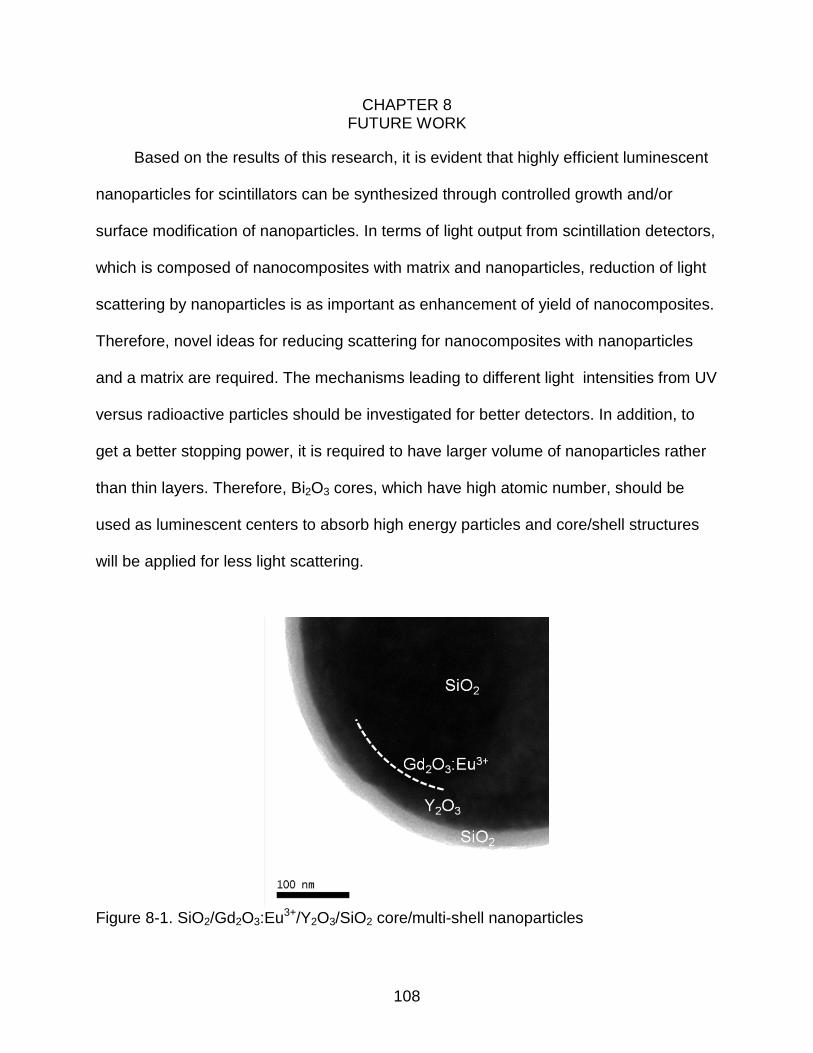
108
CHAPTER 8 FUTURE WORK
Based on the results of this research, it is evident that highly efficient luminescent
nanoparticles for scintillators can be synthesized through controlled growth and/or
surface modification of nanoparticles. In terms of light output from scintillation detectors,
which is composed of nanocomposites with matrix and nanoparticles, reduction of light
scattering by nanoparticles is as important as enhancement of yield of nanocomposites.
Therefore, novel ideas for reducing scattering for nanocomposites with nanoparticles
and a matrix are required. The mechanisms leading to different light intensities from UV
versus radioactive particles should be investigated for better detectors. In addition, to
get a better stopping power, it is required to have larger volume of nanoparticles rather
than thin layers. Therefore, Bi2O3 cores, which have high atomic number, should be
used as luminescent centers to absorb high energy particles and core/shell structures
will be applied for less light scattering.
Figure 8-1. SiO2/Gd2O3:Eu3+/Y2O3/SiO2 core/multi-shell nanoparticles
109
LIST OF REFERENCES
1. D.H. Chen and C.H. Hsieh, J. Mater. Chem. 12 (2002) 2412.
2. Z. Gui, R. Fan, W. Mo, X. Chen, L. Yang, and Y. Hu, Mater. Res. Bull. 38 (2003) 169.
3. T. Yonezawa, M. Sutoh, and T. Kunitake, Chem. Lett. 619 (1997)
4. I. Sondi, D.V. Goia, and E.J. Matijevic, J. Colloid Interface Sci. 260 (2003) 75.
5. Y. Tan, X. Dai, Y. Li, and D. Zhu, J. Mater. Chem. 13 (2003) 1069.
6. Z.L. Liu, Y.J. Liu, K.L. Yao, Z.H. Ding, J. Tao, and X. Wang, Journal of Materials Synthesis and Processing 10 (2002) 83.
7. B.L. Cushing, V.L. Kolesnichenko, and C.J. O'Connor, Chem. Rev. 104 (2004) 3893.
8. K. Nishiwaki, N. Kakuta, A. Ueno, and H. Nakabayashi, J. Catal. 118 (1989) 498.
9. B.L. Bischoff and M.A. Anderson, Chem. Mater. 7 (1995) 1772.
10. M. Niederberger, M.H. Bartl, and G.D. Stucky, Chem. Mater. 14 (2002) 4364.
11. T.P. Hoar and J.H. Schulman, Nature 152 (1943) 102.
12. J.H. Schulman and D.P. Riley, J. Colloid Sci. 3 (1948) 383.
13. Y.-X. Pang and X. Bao, J. Mater. Chem. 12 (2002) 3699.
14. P.D. Moran, J.R. Bartlett, G.A. Bowmaker, J.L. Woolfrey, and R.P. Cooney, J. Sol-Gel Sci. Technol. 15 (1999) 251.
15. Z. Wu, J. Zhang, R.E. Benfield, Y. Ding, D. Grandjean, Z. Zhang, and J. Xin, J. Phys. Chem. B 106 (2002) 4569.
16. H.S. Lee, W.C. Lee, and T. Furubayashi, J. Appl. Phys. 85 (1999) 5231.
17. N. Moumen, P. Bonville, and M.P. Pileni, Journal of Physical Chemistry 100 (1996) 14410.
18. M.L. Steigerwald, A.P. Alivisatos, J.M. Gibson, T.D. Harris, R. Kortan, A.J. Muller, A.M. Thayer, T.M. Duncan, D.C. Douglass, and L.E. Brus, Journal of the American Chemical Society 110 (1988) 3046.

110
19. X. Peng, M.C. Schlamp, A.V. Kadavanich, and A.P. Alivisatos, J. Am. Chem. Soc. 119 (1997) 7019.
20. J. Park, E.A. Kang, C.J. Bae, J.G. Park, H.J. Noh, J.Y. Kim, J.H. Park, J.H. Park, and T. Hyeon, Journal of Physical Chemistry B 108 (2004) 13594.
21. J.W. Grebinski, K.L. Richter, J. Zhang, T.H. Kosel, and M. Kuno, Journal of Physical Chemistry B 108 (2004) 9745.
22. V.F. Puntes, K.M. Krishnan, and A.P. Alivisatos, Science 291 (2001) 2115.
23. H. Yu, M. Chen, P.M. Rice, S.X. Wang, R.L. White, and S.H. Sun, Nano Letters 5 (2005) 379.
24. C.B. Murray, M. Nirmal, D.J. Norris, and M.G. Bawendi, Zeitschrift Fur Physik DAtoms Molecules and Clusters 26 (1993) S231.
25. S. Seo, H. Yang, and P.H. Holloway, J. Colloid Interface Sci. 331 (2009) 236.
26. S.-H. Kan, T. Mokari, E. Rothenberg, and U. Banin, Nature Mater. 2 (2003) 155.
27. W.E. Buhro and V.L. Colvin, Nature Mater. 2 (2003) 138.
28. W.H. Qi and M.P. Wang, Journal of Nanoparticle Research 7 (2005) 51.
29. O. Song and Z.J. Zhang, Journal of the American Chemical Society 126 (2004) 6164.
30. M. Yin, Y. Gu, I.L. Kuskovsky, T. Andelman, Y. Zhu, G.F. Neumark, and S. O'Brien, Journal of the American Chemical Society 126 (2004) 6206.
31. P.D. Cozzoli, M.L. Curri, A. Agostiano, G. Leo, and M. Lomascolo, Journal of Physical Chemistry B 107 (2003) 4756.
32. T.-K. Tseng, J. Choi, L.G. Jacobsohn, E. Yukihara, M. Davidson, and P.H. Holloway, Applied Physics A: Materials Science & Processing 100 (2010) 1137.
33. S. Ramanathan, S. Patibandla, S. Bandyopadhyay, J.D. Edwards, and J. Anderson, J. Mater. Sci.: Mater. Electron 17 (2006) 651.
34. X.G. Peng, L. Manna, W.D. Yang, J. Wickham, E. Scher, A. Kadavanich, and A.P. Alivisatos, Nature 404 (2000) 59.
35. R. Si, Y.-W. Zhang, L.-P. You, and C.-H. Yan, Angew. Chem. Int. Ed. 44 (2005) 3256.
111
36. T.A. Ring, Fundamentals of Ceramic Powder Processing and Synthesis; Academic Press: San Diego, CA (1996)
37. A.E. Nielsen, Kinetics of Precipitation; Pergamon Press: Oxford (1964)
38. H. Furedi-Milhofer, Pure Appl. Chem. 53 (1981) 2041.
39. D.A. Porter and K.E. Easterling, Phase Transfomations in Metals and Alloys, Sencond Edition, Chapman & Hall (1992)
40. G. Madras and B.J. McCoy, J. Chem. Phys. 117 (2002) 8042.
41. G. Oskam, Z. Hu, R.L. Penn, N. Pesika, and P.C. Searson, Phys. Rev. E 66 (2002) 011403.
42. V.K. LaMer and R.H. Dinegar, J. Am. Chem. Soc. 72 (1950) 4847.
43. J. Park, Angew. Chem. Int. Ed. 46 (2007) 4630.
44. J.W. Mullin, Crystallization, Butterworth-Heinemann, Wobrun, MA (1997)
45. A. Tao, P. Sinsermsuksakul, and P. Yang, Angew. Chem. Int. Ed. 45 (2006) 4597.
46. X. Peng, Adv. Mater. 15 (2003) 459.
47. G. Blasse and B.C. Grabmaier, Luminescent Materials Springer-Verlag, Berlin (1994)
48. H. Yang, C. Li, Y. Tao, J. Xu, G. Zhang, and Q. Su, Journal of Luminescence 126 (2007) 196.
49. T. Kano, Phosphor Handbook, ed. S. Shionoya and W. M. Yen, CRC Press, Boca Raton, Florida, (1998) p. 191.
50. S.Y. Seo, K.S. Sohn, H.D. Park, and S. Lee, Journal of the Electrochemical Society 149 (2002) H12.
51. H. Meyssamy, K. Riwotzki, A. Kornowski, S. Naused, and M. Haase, Advanced Materials 11 (1999) 840.
52. F. Vetrone, J.C. Boyer, J.A. Capobianco, A. Speghini, and M. Bettinelli, Chemistry of Materials 15 (2003) 2737.
53. J. Hu, L.-s. Li, W. Yang, L. Manna, L.-w. Wang, and A.P. Alivisatos, Science 292 (2001) 2060.
54. S. Shionoya, Phosphor Handbook, ed. S. Shionoya and W. M. Yen, CRC Press, Boca Raton, Florida, (1998) p. 7.
112
55. C. Feldmann, T. Jtel, C.R. Ronda, and P.J. Schmidt, Adv. Funct. Mater. 13 (2003) 511.
56. H. Henning, Angew. Chem. Int. Ed. 48 (2009) 3572.
57. H. Chander, Materials Science and Engineering: R: Reports 49 (2005) 113.
58. U. Kaufmann, M. Kunzer, K. Kohler, H. Obloh, W. Pleschen, P. Schlotter, J. Wagner, A. Ellens, W. Rossner, and M. Kobuschi, Phys. Status Solidi A 192 (2002) 246.
59. S. Nakamura and G. Fasol, The Blue Laser Diode, Springer, Berlin (1997)
60. D. Bera, S. Maslov, L. Qian, J.S. Yoo, and P.H. Holloway, Journal of Display Technology 6 (2010) 645.
61. A. Henning and D. Höppe, Angewandte Chemie International Edition 48 (2009) 3572.
62. K. Kohmoto, Phosphor Handbook, ed. S. Shionoya and W. M. Yen, CRC Press, Boca Raton, Florida, (1998) p. 361.
63. A.n. Sigma Aldrich - Detectors in Nuclear Medical Imaging - High Purity Crystals for Scintillation,
64. P. Lecoq, A. Annenkov, A. Gektin, M. Korzhik, and C. Pedrini, Inorganic Scintillators for Detector Systems, Springer (2006)
65. A. Lushchik, M. Kirm, C. Lushchik, I. Martinson, and G. Zimmerer, J. Lumin. 87-89 (2000) 232.
66. P.A. Rodnyi, P. Dorenbos, and C.W.E.v. Eijk, Phys. Status Solidi B 187 (1995) 29.
67. A.N. Vasil'ev, Nucl. Instr. Meth. Phys. Res. B 107 (1996) 165.
68. R.H. Bertram and A. Lempicki, J. Lumin. 68 (1996) 225.
69. C.V. Eijk, Inorganic-scintillator requirements, in record of the Int. Workshop Physical Processes in Fast Scintillator, Stratech Report TUD, Delft, The Netherlands (1994)
70. P. Lecomte, D. Luckey, F. Nessi-Tedaldi, F. Pauss, and D. Renker, Nuclear Instruments & Methods in Physics Research, Section A: Accelerators, Spectrometers, Detectors, and Associated Equipment 587 (2008) 266.
71. P.J. Shlichta, in Nuclear Science Symposium Conference Record, IEEE p.367. (2001)
113
72. T.M. Blodgett, C.C. Meltzer, and D. W. Townsend, Radiology 242 (2007) 360.
73. C.M.L. West, T. Jones, and P. Price, Nature Reviews Cancer 4 (2004) 457.
74. C.L. Melcher and J.S. Schweitzer, Nucl. Instr. Meth. Phys. Res. 314 (1992) 212.
75. Y. Masumoto, Phosphor Handbook, ed. S. Shionoya and W. M. Yen, CRC Press, Boca Raton, Florida (1998) p. 72.
76. A.P. Alivisatos, Science 271 (1996) 933.
77. J. Lefebvre, P.J. Poole, J. Fraser, G.C. Aers, D. Chithrani, and R.L. Williams, Journal of Crystal Growth 234 (2002) 391.
78. Q. Pang, L. Zhao, Y. Cai, D.P. Nguyen, N. Regnault, N. Wang, S. Yang, W. Ge, R. Ferreira, G. Bastard, and J. Wang, Chemistry of Materials 17 (2005) 5263.
79. A.G. Rolo, M.I. Vasilevskiy, N.P. Gaponik, A.L. Rogach, and M.J.M. Gomes, Physica Status Solidi B: Basic Research 229 (2002) 433.
80. C.B. Murray, D.J. Norris, and M.G. Bawendi, J. Am. Chem. Soc. 115 (1993) 8706.
81. I. Yu, T. Isobe, and M. Senna, Journal of Physics and Chemistry of Solids 57 (1996) 373.
82. D.R. Vij, Luminescence of Solids (Plenum Press, New York) (1988)
83. R.N. Bhargava, D. Gallagher, X. Hong, and A. Nurmikko, Phys. Rev. Lett. 72 (1994) 416.
84. M. Ihara, T. Igarashi, T. Kusunoki, and K. Ohno, J. Electrochem. Soc. 149 (2002) H72.
85. U. Kolitsch, H.J. Seifert, and F. Aldinger, J of Alloys and Compounds 257 (1997) 104.
86. A.M. Pires, M.F. Santos, M.R. Davolos, and E.B. Stucchi, J of Alloys and Compounds 344 (2002) 276.
87. B.L. Abrams and P.H. Holloway, Chem. Rev 104 (2004) 5783.
88. H. Yang and P.H. Holloway, Appl. Phys. Lett. 82 (2003) 1965.
89. M.A. Hines and P. GnyotSionnest, J. Phys. Chem. 100 (1996) 468.
114
90. B.O. Dabbousi, J. RodriguezViejo, F.V. Mikulec, J.R. Heine, H. Mattoussi, R. Ober, K.F. Jensen, and M.G. Bawendi, J. Phys. Chem. B 101 (1997) 9463.
91. K. Song and S. Lee, Curr. Appl. Phys. 1 (2001) 169.
92. C.F. Hoener, K.A. Allan, A.J. Bard, A. Campion, M.A. Fox, T.E. Mallouk, S.E. Webber, and J.M. White, J. Phys. Chem. 96 (1992) 3812.
93. A.R. Kortan, R. Hull, R.L. Opila, M.G. Bawendi, M.L. Steigerwald, P.J. Carroll, and L.E. Brus, J. Am. Chem. Soc. 112 (1990) 1327.
94. P. Reiss, J. Bleuse, and A. Pron, Nano Lett. 2 (2002) 781.
95. M. Chang and S. Tie, Nanotechnology 19 (2008) 075711.
96. M. Darbandi, W. Hoheisel, and T. Nann, Nanotechnology 17 (2006) 4168.
97. G. Pan, H. Song, X. Bai, L. Fan, H. Yu, Q. Dai, B. Dong, R. Qin, S. Li, S. Lu, X. Ren, and H. Zhao, J. Phys. Chem. C 111 (2007) 12472.
98. G.H. Pan, H.W. Song, X. Bai, Z.X. Liu, and H.Q. Yu, Chem. Mater. 18 (2006) 4526.
99. M. Yu, J. Lin, and J. Fang, Chem. Mater. 17 (2005) 1783.
100. H. Zhu and D. Zuo, The Journal of Physical Chemistry C 113 (2009) 10402-10406.
101. F. Wang, Y. Zhang, X. Fan, and M. Wang, Nanotechnology 17 (2006) 1527.
102. K.W. Kramer, P. Dorenbos, H.U. Gudel, and C.W.E.v. Eijk, J. Mater. Chem. 16 (2006) 2773.
103. S. Srivastava and N.A. Kotov, Soft Matter 5 (2009) 1146.
104. E.V. Shevchenko, D.V. Talapin, A.L. Rogach, A. Kornowski, M. Haase, and H. Weller, J.Am. Chem. Soc. 124 (2002) 11480.
105. B. Pietrobon, M. McEachran, and V. Kitaev, ACS Nano 3 (2009) 21.
106. C. Burda, X. Chen, R. Narayanan, and M.A. El-Sayed, Chem. Rev. 105 (2005) 1025.
107. Z.W. Pan, Z.R. Dai, and Z.L. Wang, Science 291 (2001) 1947.
108. Y. Zhang, G. Li, and L. Zhang, Chem. Lett. 33 (2004) 334.
115
109. M.-P. Pileni, Nat. Mater. 2 (2003) 145.
110. V. Polshettiwar, B. Baruwati, and R.S. Varma, ACS Nano 3 (2009) 728.
111. A.K. H. Meyssamy K. Riwotzki, S. Naused and M. Haase, Advanced Materials 11 (1999) 840.
112. H.S. Yang, H. Lee, and P.H. Holloway, Nanotechnology 16 (2005) 2794.
113. M. Yada, M. Mihara, S. Mouri, M. Kuroki, and T. Kijima, Advanced Materials 14 (2002) 30971.
114. T.-K. Tseng, J. Choi, L.G. Jacobsohn, E.D. Yukihara, Mark, and P.H. Holloway, Applied Physics A: Materials Science & Processing 100 (2010) 1137.
115. M. Bruchez, M. Moronne, P. Gin, S. Weiss, and A.P. Alivisatos, Science 281 (1998) 2013.
116. W.C.W. Chan and S.M. Nie, Science 281 (1998) 2016.
117. Z. Huanga, P. Thomsonb, and S. Di, Journal of Physics and Chemistry of Solids 68 (2007) 530.
118. G. Brauer, Handbook of Preparative Inorganic Chemistry, second ed., Academic Press, New York, (1963)
119. H. Chen, J. Zhang, X. Wang, S. Gao, M. Zhang, Y. Ma, Q. Dai, D. Li, S. Kan, and Guangtian Zou, Journal of Colloid and Interface Science 297 (2006) 130.
120. H.E. Hoefdraad, J. Solid State Chem. 15 (1975) 175.
121. J. Heber, K.H. Hellwege, U. Kobler, and H. Murmann, Z. Phys. 237 (1970) 189.
122. J. Choi, T.-K. Tseng, M. Davidson, and P.H. Holloway, J. Mater. Chem. 21 (2011) 3113.
123. H. Zhu and D. Zuo, J. phys. Chem. C 113 (2009) 10402.
124. J. Dexpertghys, M. Faucher, and P. Caro, Phys. Rev. B 23 (1981) 607.
125. S.C. Erwin, L. Zu, M.I. Haftel, A.L. Efros, T.A. Kennedy, and D.J. Norris, Nature 436 (2005) 91.
126. A.P. Alivisatos, K.P. Johnson, X. Peng, T. Wilson, C.J. Loweth, M.P.B. Jr, and P.G. Schultz, Nature (London) 382 (1996) 609.
116
127. G.C. Kim, S.I. Mho, and H.L. Park, J. Mater. Sci. Lett 51 (1995) 107.
128. L. Ozawa, Mater. Chem. Phys. 51 (1997) 107.
129. M.H. Lee, S.G. Oh, S.C. Yi, D.S. Seo, and J.S. Yoo, J. Electrochem. Soc. 147 (2000) 3139.
130. A.G. Macedo, D. Ananias, P.S. Andre, R.A.S. Ferreira, A.L. Kholkin, L.D. Carlos, and J. Rocha, Nanotechnology 19 (2008) 295702.
131. W. Bu, Z. Hua, H. Chen, and J. Shi, J. Phys. Chem. B 109 (2005) 14461.
132. G. Liu, G. Hong, and D. Sun, J. Colloid Interface Sci. 278 (2004) 133.
133. D.V. Talapin, A.L. Rogach, A. Kornowski, M. Haase, and H. Weller, Nano Lett. 1 (2001)
134. L. Manna, E.C. Scher, L.S. Li, and A.P. Alivisatos, J. Am. Chem. Soc. 124 (2002) 7136.
135. F. Fievet, Surfactant Sci. Ser. 92 (2000) 460.
136. H. Yang and Y. Kim, J. Lumin. 128 (2008) 1570.
137. Z.L. Wang, Z.W. Quan, P.Y. Jia, C.K. Lin, Y. Luo, Y. Chen, J. Fang, W. Zhou, C.J. O’Conner, and J. Lin, Chem. Mater. 18 (2006) 2030.
138. Y.W. Cao and U.J. Banin, J. Am. Chem. Soc. 122 (2000) 9692.
139. P.H. Holloway, J. Vac. Sci. Technol. (N. Y., NY, U. S.), (1975) 392.
140. C.J. Powell, Surf. Sci. 44 (1974) 29.
141. W.W. Zhang, W.P. Zhang, P.B. Xie, M. Yin, H.T. Chen, L. Jing, Y.S. Zhang, L.R. Lou, and S.D. Xia, J. Colloid Interface Sci. 262 (2003) 588.
142. G. Wakefield, H.A. Keron, P.J. Dobson, and J.L. Hutchison, J. Colloid Interface Sci. 215 (1999) 179.
143. C. Louis, R. Bazzi, M.A. Flores, W. Zhang, K. Lebbou, O. Tillement, B. Mercier, C. Dujardin, and P. Perriat, J. Solid State Chem. 173 (2003) 335.
144. J. Li, X. Li, X. Sun, and T.J. Ishigaki, J. Phys. Chem. C 112 (2008) 11707.
145. T. Tseng, J. Choi, M. Davidson, and P.H. Holloway, J. Mater. Chem. 20 (2010) 6111.
146. D.K. Williams, H. Yuan, and B.M. Tissue, J. Lumin. 83 (1999) 297.

117
147. J.K. Park, K.N. Kim, P.K. Bae, J.H. Lee, C.H. Han, and C.H. Kim, Electrochem. Solid-State Lett. 10 (2007) J97.
148. E. Nakazawa, Phosphor Handbook, ed. S. Shionoya and W. M. Yen, CRC Press, Boca Raton, Florida, (1998) p. 85.
149. D.R.G.J.D. Bryan, Prog. Inorg. Chem. pp. 47-126 (2005)
150. L. Qian, D. Bera, T.-K. Tseng, and P.H. Holloway, Appl. Phys. Lett. 94 (2009) 073112.
151. G. Bonnet, M. Lachkar, J.P. Larpin, and J.C. Colson, Solid States Ionics 72 (1994) 344.
152. G. Bonnet, M. Lachkar, J.P. Larpin, and J.C. Colson, Thin Solid Film 261 (1995) 31.
153. M. Yu, J. Lin, and J. Fang, Chem. Mater. 17 (2005) 1783.
154. D.Y. Kong, M. Yu, C.K. Lin, X.M. Liu, J. Lin, and J. Fang, J. Electrochem. Soc. 152 (2005) H146.
155. W. Stöber, A. Fink, and E. Bohn, J. Colloid Interface Sci. 26 (1968) 62.
156. Y. Huang and J.E. Pemberton, colloids and surfaces A 360 (2010) 175.
157. A.K.V. Helden, J.W. Jansen, and A. Vrij, J. Colloid Interface Sci. 81 (1981) 354.
158. C.J. Powell, Surface and Microanalysis Science Division, National Institute of Standards and Technology, Gaithersburg, MD 20899, USA
159. L. Porres, A. Holland, L.-O. Palsson, A. Monkman, C. Kemp, and A. Beeby, J. Fluoresc. 16 (2006) 267.
160. L.-O. Pålsson and A. Monkman, Adv. Mater. 14 (2002) 757.
161. S. Li, H. Song, H. Yu, S. Lu, X. Bai, G. Pan, Y. Lei, L. Fan, and T. Wang, Journal of Luminescence 122 (2007) 876.
162. Z. Deng, L. Cao, F. Tang, and B. Zou, J. Phys. Chem. B 109 (2005) 16671.
163. C. Li, C. Wyon, and R. Moncorge, IEEE J. Quant. Electron. 28 (1992) 1209.
164. T.E. Peters, J. Electrochem. Soc. (1969) 985.
165. M. Kobayashi and M. Ishii, Nucl. Instr. Meth. B 61 (1994) 591.

118
166. H. Ishibashi and Y.K.e. al., Crystal 2000 Proc. Int. Workshop (1993) p. 389.
167. T. Ye, G.W. Zhao, and W.P. Zhang, Mter. Res. Bull. 32 (1997) 501.
168. M.D. Dramicanin, V. Jokanovic, B. Vian, E. Antic-Fidancev, M. Mitric, and Z. Andric, J of Alloys and Compounds 424 (2006) 213.
169. R.E. Muenchausen, E.A. McKigney, L.G. Jacobsohn, M.W. Blair, B.L. Bennett, and D.W. Cooke, IEEE Transactions on Nuclear Science 55 (2008) 1532.
170. M.D. Dramicanin, B. Vian, Z. Andric, V. Djokovic, and A.S. Luyt, J of Alloys and Compounds 464 (2008) 357.
171. W. Zhang, P. Xie, C. Duan, K. Yan, M. Yin, L. Lou, S. Xia, and J.C. Krupa, Chem. Phys. Lett. 292 (1998) 133.
172. D.W. Cooke, K.J. McClellan, B.L. Bennett, J. M. Roper, M.T. Whittaker, R.E. Muenchausen, and R.C. Sze, J. Appl. Phys. 88 (2000) 7360.
173. M. Sekita, Y. Miyazawa, T. Akahane, and T. Chiba, J. Appl. Phys. 66 (1989) 373.
174. S. Tanimizu, Phosphor Handbook, ed. S. Shionoya and W. M. Yen, CRC Press, Boca Raton, Florida (1998) p. 186.
175. M.S. Zucker, Nuclear Instruments and Methods in Physics Research Section A: Accelerators, Spectrometers, Detectors and Associated Equipment 242 (1986) 306.
176. G.M. Onyshchenko, L.L. Nagornaya, V.G. Bondar, Y. Borodenko, O.V. Zelenskaya, E.N. Pirogov, and V.D. Ryzhikov, Nuclear Instruments and Methods in Physics Research A 537 (2005) 394.
119
BIOGRAPHICAL SKETCH
Jihun Choi was born in Chungcheong-do, South Korea in 1977. His family moved
to Seoul at an early age where he grew up and was educated. His access to the
laboratory environment began at Chungdong high school when he was a chief of the
Chemistry Club. He entered the Department of Material Science and Engineering at
Seoul National University in 1997 and obtained his bachelor’s degree in 2002. He
continued his study and obtained his Master of Science degree in 2004. His research
topic for the M.S. was “Enhanced electrical properties of HfAlO high-k dielectric thin
films for a gate oxide of Si MOSFET devices”. After graduation with the M.S., he was
hired by LG Electronics Institute of Technology (R&D campus in Seoul) as a research
engineer. His research field at LG Electronics was the development of flexible displays
with organic transistors. In 2007, he was admitted to the Department of Materials
Science and Engineering at the University of Florida to pursue his Ph.D. degree with a
specialty in electronic materials. His research interests at Dr. Holloway’s group were
synthesis and characterization of highly efficient luminescent nanoparticles for an
application of scintillator radiation detectors. He received his Ph.D. degree in August of
2011 in Materials Science and Engineering.