Engineering the Power Delivery Network
16
1 C HAPTER 1 Engineering the Power Delivery Network 1.1 What Is the Power Delivery Network (PDN) and Why Should I Care? The power delivery network consists of all the interconnects in the power supply path from the voltage regulator modules (VRMs) to the circuits on the die. Generally, these include the power and ground planes in the boards, cables, connectors, and all the capacitors associated with the power supply. Figure 1.1 is an example of a typical computer board with multiple VRMs and paths delivering the power and ground to the pads of all the active devices.
Transcript of Engineering the Power Delivery Network

1
C H A P T E R 1
Engineering the Power Delivery Network
1.1 What Is the Power Delivery Network (PDN) and Why Should I Care?The power delivery network consists of all the interconnects in the power supply path from the voltage regulator modules (VRMs) to the circuits on the die. Generally, these include the power and ground planes in the boards, cables, connectors, and all the capacitors associated with the power supply. Figure 1.1 is an example of a typical computer board with multiple VRMs and paths delivering the power and ground to the pads of all the active devices.
9780132735551_print.indb 19780132735551_print.indb 1 23/02/17 9:07 PM23/02/17 9:07 PM

2 Chapter 1 • Engineering the Power Delivery Network
Figure 1.1 A typical computer motherboard with multiple VRMs and active devices. The PDN includes all the interconnects from the pads of the VRMs to the circuits on the die.
The purpose of the PDN is to
• Distribute low-noise DC voltage and power to the active devices doing all the work.
• Provide a low-noise return path for all the signals.• Mitigate electromagnetic interference (EMI) problems without contrib-
uting to radiated emissions.
In this book, we focus on the fi rst role of the PDN: to distribute a DC voltage and power to all the active devices requiring power and to keep the noise below an acceptable level. Unsuccessful noise control on the PDN will contribute to contraction of the eye of any signal. The amplitude of the eye in the vertical direction collapses from voltage noise. The time of the signal crossing a reference spreads out in the horizontal direction creating jitter and reduction of the eye opening. Internal core circuits might suffer setup and hold-time errors, leading to functional failures.
9780132735551_print.indb 29780132735551_print.indb 2 23/02/17 9:07 PM23/02/17 9:07 PM

What Is the Power Delivery Network (PDN) and Why Should I Care? 3
T I P The consequence of not correctly designing the PDN is increased bit error ratios from enhanced vertical noise and jitter on both I/O circuits and internal-to-the-chip circuits. Excessive horizontal noise in core circuits might lead to setup and hold-time violations.
Depending on the circuit of the switching gates, the PDN noise will add to the signal coming from the transmitter (TX). This can also appear as noise on the voltage reference at the receiver (RX). In both cases, the PDN noise will reduce the noise margin available from other sources.
Figure 1.2 shows an example of the measured voltage noise between the core power and ground (Vdd and Vss) rails on a microprocessor die at three different on-die locations and two different voltage rails. In this example, the voltage noise is 125 mV. In many circuits, a large fraction of this voltage noise will appear superimposed on the signal at the RX.
2 µsec
Clock period is 3 nsec
200 ns/div –94.000 ns
125 mV
Figure 1.2 Example of the noise between the Vdd and Vss rails in a microprocessor running at 300 MHz clock, measured at three different locations. More than 125 mV of noise is present.
Even if this noise by itself is not enough to cause a bit failure, it will contribute to eye closure, and with the other noise sources might result in a failure.
Voltage noise on the power rails of the chips also affects timing. The propagation delay, the time from which an input voltage transition propagates
9780132735551_print.indb 39780132735551_print.indb 3 23/02/17 9:07 PM23/02/17 9:07 PM

4 Chapter 1 • Engineering the Power Delivery Network
through the sequence of gates contributing to an output voltage transition, depends on the instantaneous voltage level between the In CMOS technology, the higher the drain-to-source voltage, the larger the electric fi elds in the chan-nels and the shorter the propagation delay. Likewise, the lower the Vdd to Vss voltage, the longer the propagation delay.
This means that voltage noise on the Vdd to Vss rails on die directly con-tributes to timing variations in the output signals called jitter. A higher voltage on the Vdd rail “pulls in” a clock edge, whereas a lower rail voltage “pushes out” a clock edge. Figure 1.3 is an example of the measured jitter induced on a high-end FPGA test chip from voltage noise on the PDN.
Figure 1.3 Measured jitter on a clock signal in the presence of Vdd to Vss voltage noise.
M01_Bogatin_Ch01_p001-016.indd 4M01_Bogatin_Ch01_p001-016.indd 4 23/02/17 9:14 PM23/02/17 9:14 PM
Engineering the PDN 5
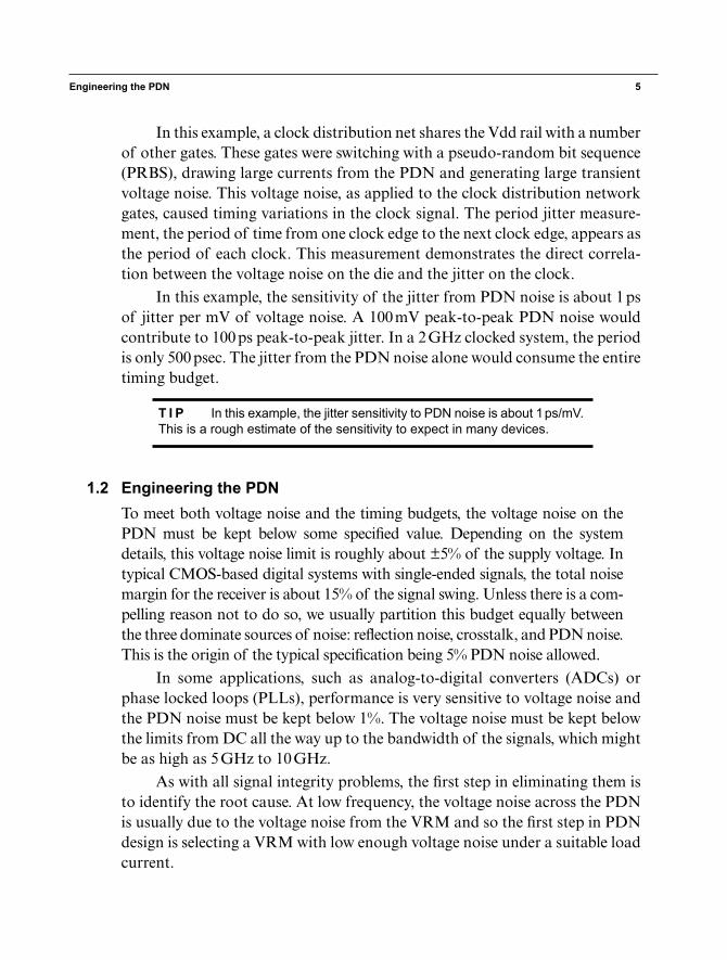
In this example, a clock distribution net shares the Vdd rail with a number of other gates. These gates were switching with a pseudo-random bit sequence (PRBS), drawing large currents from the PDN and generating large transient voltage noise. This voltage noise, as applied to the clock distribution network gates, caused timing variations in the clock signal. The period jitter measure-ment, the period of time from one clock edge to the next clock edge, appears as the period of each clock. This measurement demonstrates the direct correla-tion between the voltage noise on the die and the jitter on the clock.
In this example, the sensitivity of the jitter from PDN noise is about 1 ps of jitter per mV of voltage noise. A 100 mV peak-to-peak PDN noise would contribute to 100 ps peak-to-peak jitter. In a 2 GHz clocked system, the period is only 500 psec. The jitter from the PDN noise alone would consume the entire timing budget.
T I P In this example, the jitter sensitivity to PDN noise is about 1 ps/mV. This is a rough estimate of the sensitivity to expect in many devices.
1.2 Engineering the PDNTo meet both voltage noise and the timing budgets, the voltage noise on the PDN must be kept below some specifi ed value. Depending on the system details, this voltage noise limit is roughly about ±5% of the supply voltage. In typical CMOS-based digital systems with single-ended signals, the total noise margin for the receiver is about 15% of the signal swing. Unless there is a com-pelling reason not to do so, we usually partition this budget equally between the three dominate sources of noise: refl ection noise, crosstalk, and PDN noise. This is the origin of the typical specifi cation being 5% PDN noise allowed.
In some applications, such as analog-to-digital converters (ADCs) or phase locked loops (PLLs), performance is very sensitive to voltage noise and the PDN noise must be kept below 1%. The voltage noise must be kept below the limits from DC all the way up to the bandwidth of the signals, which might be as high as 5 GHz to 10 GHz.
As with all signal integrity problems, the fi rst step in eliminating them is to identify the root cause. At low frequency, the voltage noise across the PDN is usually due to the voltage noise from the VRM and so the fi rst step in PDN design is selecting a VRM with low enough voltage noise under a suitable load current.
9780132735551_print.indb 59780132735551_print.indb 5 23/02/17 9:07 PM23/02/17 9:07 PM

6 Chapter 1 • Engineering the Power Delivery Network
However, even with the world’s most stable VRM, voltage noise still exists on the pads of the die. This arises from the voltage drop across the impedance of the entire PDN from transient power currents through the gates on the die. Between the pads of the VRM and the pads on the die are all the interconnects associated with the PDN. We refer to this entire network as the PDN ecology.
T I P The PDN ecology is the entire series of interconnects from the pads on the die to the pads of the VRM. These all interact to create the impedance profi le applied to the die and infl uence PDN noise.
As applied to the pads of the die, these interconnects contribute to an impedance profi le. Figure 1.4 shows a typical example.
1
1E1
1E–1
1E–2
1E–3
Impe
danc
e, Ω
1E3 1E4 1E5 1E6 1E7 1E8 1E9
Frequency, Hz
Figure 1.4 Example of an impedance profi le of the entire PDN ecology, as applied to the pads of the die.
Any transient currents through this impedance profi le generates voltage noise on the pads of the chip, independent of the VRM stability.
For example, Figure 1.5 shows the transient current spectrum drawn by the core power rail for a device when executing a specifi c microcode. Super-imposed on the current spectrum is the impedance profi le through which this current fl ows. The combination of the current amplitude and impedance at each frequency generates a voltage noise spectrum. This noise spectrum, when viewed in the time domain, results in a transient voltage noise.
9780132735551_print.indb 69780132735551_print.indb 6 23/02/17 9:07 PM23/02/17 9:07 PM

Engineering the PDN 7
1.3
1.2
1.1
1.0
0.9
0.8
0.7
0.0 0.2 0.4 0.6 0.8 1.0
Volt
age
on
ch
ip
1.3
1.2
1.1
1.0
0.9
0.8
0.7
Volt
age
on
ch
ip
Time, µsec0.0 0.2 0.4 0.6 0.8 1.0
Time, µsec
“Working” “Failed!”
1
1E1
1E–1
1E–2
1E–3
1
1E1
1E–1
1E–2
1E–31E2 1E3 1E4 1E5 1E6 1E7 1E8 1E9
Frequency, Hz1E2 1E3 1E4 1E5 1E6 1E7 1E8 1E9
Frequency, Hz
Cur
rent
, im
peda
nce
Cur
rent
, im
peda
nce
Figure 1.5 Left Side: PDN impedance profi le and transient current spectrum result in acceptable voltage noise. Right Side: Slight change in current spectrum gives unacceptable voltage noise.
The left side of Figure 1.5 shows the transient current spectrum, PDN impedance profi le, and resulting voltage noise on the power rail. This com-bination of current spectral peaks and impedance peaks results in acceptable noise. On the right is the same impedance profi le, but with slightly different microcode algorithm driving the same gates at a slightly different frequency. A current spectral peak ended up overlapping a larger impedance peak and generating a rail voltage noise above the acceptable limit.
The actual voltage noise generated by the transient current through the impedance profi le depends on the overlap of the current frequency components and the peaks in the impedance profi le. If the voltage noise is below a specifi ed level, PDN induced errors will not occur. If the microcode changes resulting current amplitude peaks and frequency component changes, their overlap with impedance peaks might create more voltage noise and product failure.
T I P The noise on the PDN depends as much on the impedance profi le applied to the die as the spectrum of the transient current through the die. Microcode details and gate utilization have a strong impact on the PDN noise generated.
9780132735551_print.indb 79780132735551_print.indb 7 23/02/17 9:07 PM23/02/17 9:07 PM

8 Chapter 1 • Engineering the Power Delivery Network
1.3 “Working” or “Robust” PDN DesignThe variability in performance due to the specifi c microcode driving the switching of on-die gates makes testing a product for adequate PDN design diffi cult. A product might work just fi ne at boot up, or when running a specifi c software test suite if the combination of current spectral peaks and impedance peaks results in less than the specifi ed transient noise. The product design may “pass” this test and be stamped as “working.”
However, if another software suite were to run that drives more gates and causes them to switch at a different dominant loop frequency, which coincidently overlaps a peak in the PDN impedance profi le, larger instanta-neous voltage drops might result and the same product could fail.
Although having the product boot up, run a test suite and apparently work is encouraging, it does not guarantee “robust” operation. Products often “work” in evaluation but have fi eld failures when driven by a broad range of customer software.
A robust PDN design means that any software code may run and gener-ate the maximum transient current at any arbitrary frequency with any time domain signature. The resulting worst-case voltage generated by this current through the impedance profi le is always less than an amount that would cause a failure.
The combination of the worst-case transient current and the voltage noise specifi cation work together to set a limit for the maximum allowable PDN impedance such that the voltage noise will never exceed the specifi cation.
This maximum allowable PDN impedance with guaranteed performance is referred to as the target impedance in PDN design, and we derive it with [1]
ZV
Itargetnoise
max transient
= Δ−
(1.1)
where
Ztarget = the maximum allowable PDN impedance at any frequency
∆Vnoise = the maximum specifi ed voltage rail noise to meet performance requirements
Imax-transient = the worst-case transient current under any possible operation
9780132735551_print.indb 89780132735551_print.indb 8 23/02/17 9:07 PM23/02/17 9:07 PM
“Working” or “Robust” PDN Design 9
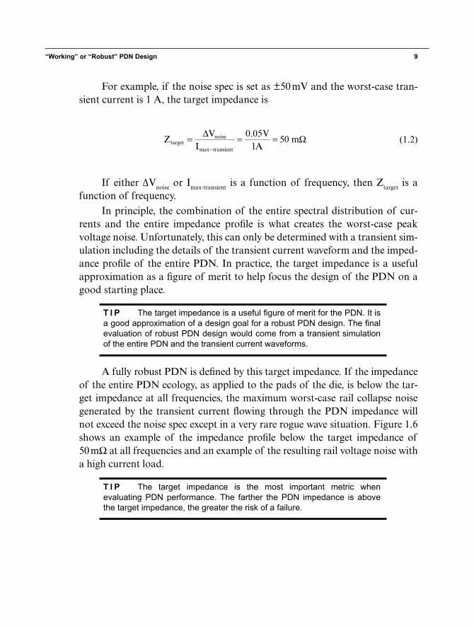
For example, if the noise spec is set as ±50 mV and the worst-case tran-sient current is 1 A, the target impedance is
ZV
I0.05V
1A50 mtarget
noise
max transient
= Δ = = Ω−
(1.2)
If either ∆Vnoise or Imax-transient is a function of frequency, then Ztarget is a function of frequency.
In principle, the combination of the entire spectral distribution of cur-rents and the entire impedance profi le is what creates the worst-case peak voltage noise. Unfortunately, this can only be determined with a transient sim-ulation including the details of the transient current waveform and the imped-ance profi le of the entire PDN. In practice, the target impedance is a useful approximation as a fi gure of merit to help focus the design of the PDN on a good starting place.
T I P The target impedance is a useful fi gure of merit for the PDN. It is a good approximation of a design goal for a robust PDN design. The fi nal evaluation of robust PDN design would come from a transient simulation of the entire PDN and the transient current waveforms.
A fully robust PDN is defi ned by this target impedance. If the impedance of the entire PDN ecology, as applied to the pads of the die, is below the tar-get impedance at all frequencies, the maximum worst-case rail collapse noise generated by the transient current fl owing through the PDN impedance will not exceed the noise spec except in a very rare rogue wave situation. Figure 1.6 shows an example of the impedance profi le below the target impedance of 50 mΩ at all frequencies and an example of the resulting rail voltage noise with a high current load.
T I P The target impedance is the most important metric when evaluating PDN performance. The farther the PDN impedance is above the target impedance, the greater the risk of a failure.
9780132735551_print.indb 99780132735551_print.indb 9 23/02/17 9:07 PM23/02/17 9:07 PM

10 Chapter 1 • Engineering the Power Delivery Network
Target impedance
PDN impedance profile
Power rail voltage
Transient chip current
Vol
tage
Frequency, Hz
Impe
danc
e, Ω
1E2 1E3 1E4 1E5 1E6 1E7 1E8 1E9 1E10
1E–3
1E–2
1E–1
1E1
1
1.2
1.0
0.8
0.6
0.4
0.2
0.0
–0.2
0 20 40 60 80 100Time, nsec
Figure 1.6 Top: The impedance profi le of the PDN ecology engineered to be below the target impedance from DC up to a very high bandwidth. Bottom: The resulting Vdd rail noise under large transient current load showing the noise is always below the 5% spec limit. The square wave trace is the transient current as driven by a clock. It is plotted on a relative scale.
In practice, the maximum, worst-case transient current through the die will not be fl at at all frequencies. The maximum current amplitude generally drops off at the high-frequency end, related to how quickly the maximum number of switching gates can be turned on. The precise details depend on the chip architecture, the number of bits in the pipeline, and the nature of the microcode. The effective rise time could be from the rise time of the clock edge to 100 clock cycles.
For example, if the clock frequency is 2 GHz, with a 0.5 ns clock period, and the maximum number of switching gates requires 20 cycles to build up, the shortest rise time for the turn on of the worst-case transient current would be 0.5 ns × 20 cycles = 10 ns. The amplitude of the maximum transient current frequency components will begin to roll off above about 0.35/10 ns = 35 MHz.
9780132735551_print.indb 109780132735551_print.indb 10 23/02/17 9:07 PM23/02/17 9:07 PM

“Working” or “Robust” PDN Design 11
Above 35 MHz, the worst-case transient current spectrum would drop off at −20 dB/decade and the resulting target impedance would increase with fre-quency. The target impedance, in this example, assuming a 50 mV rail voltage noise spec and worst-case current amplitude of 1 A, is shown in Figure 1.7.
Frequency, Hz
Targ
et im
ped
ance
, Ω
1.E+04 1.E+05 1.E+06 1.E+07 1.E+08 1.E+09 1.E+10
100
10
1
0.1
0.01
Figure 1.7 Target impedance when the transient current turns on in 20 clock cycles to a maximum of 1 A.
The consequence of this behavior is that the target impedance spec is relaxed at higher frequency. Estimating where this knee frequency begins is often diffi cult unless we know the details of the transient current and worst-case microcode.
This analysis points out that, in practice, accurately calculating the tran-sient currents and the precise requirements for the target impedance of the PDN is extremely diffi cult. One must always apply engineering judgment in translat-ing the information available into the requirements for a cost-effective design.
The process to engineer the PDN is to
• Establish a best guess for the target impedance based on what is known about the functioning and applications of the chips.
• Make engineering decisions to try to meet this impedance profi le where possible.
• Balance the trade-offs between the cost of implementing the PDN impedance compared to the target impedance, and the risk of a fi eld failure.
9780132735551_print.indb 119780132735551_print.indb 11 23/02/17 9:07 PM23/02/17 9:07 PM

12 Chapter 1 • Engineering the Power Delivery Network
A rough measure of the risk of a failure of circuits to run at rated per-formance is the ratio of the actual PDN impedance to the target impedance, termed the PDN ratio:
=PDN ratioActual PDN Impedance
Target Impedance (1.3)
A ratio of less than 1 indicates low risk of a PDN-related failure. As this ratio increases, the risk increases as well. From practical experience, a ratio of 2 might still offer an acceptable risk, but a ratio of 10 will almost surely result in unacceptable risk. Even though many microcodes run at rated performance, some are likely to stimulate the PDN resonance and generate product stability issues.
Generally, achieving a lower impedance PDN, and consequently a lower risk ratio, costs more either due to more components required, tighter assembly design rules impacting yield, more layers in the board or package, increased area for die capacitance, or the use of more expensive materials. The balance between cost and risk is often a question of how much risk you are comfortable with. By paying more for added design margin, you can always “buy insurance” and reduce the risk. This is the fundamental trade-off in PDN design.
T I P An important metric of risk in PDN design is the PDN ratio, which is the ratio of the peak impedance to the target impedance. A PDN ratio of 2 or lower is a low risk whereas a PDN ratio of 10 or more is a high risk.
In consumer applications, often strongly cost driven, engineering for a higher risk ratio with a lower cost design might be a better balance. However, in avionic systems, for example, paying extra for a risk ratio less than 1 might be the cost-effective solution. Different applications have a different balance between cost and risk ratio.
1.4 Sculpting the PDN Impedance Profi leThe goal in PDN design is to engineer an acceptable impedance profi le from DC to the highest frequency component of any power rail currents. All the elements of the PDN should be engineered together to sculpt the
9780132735551_print.indb 129780132735551_print.indb 12 23/02/17 9:07 PM23/02/17 9:07 PM

Sculpting the PDN Impedance Profi le 13
impedance profi le of the entire ecology. Although many elements interact, assigning some features of the PDN impedance profi le to specifi c features in the PDN design is possible.
Figure 1.8 shows a simplifi ed schematic of the entire PDN ecology. This includes the on-die capacitance, the possibility of on-package capacitors, the package lead inductance, the circuit board vias, the power and ground planes in the circuit board, decoupling capacitor, bulk capacitors, and VRM.
Ref
LPFBalls& vias
Bulk cap SMT capsOn-diecapacitors
VRM
Imp
edan
ce, Ω
Package lead inductance
On-chipcapacitance
Packagecapacitor
Bumps
Load
Packagepower planes
PCBplanes& vias
PCBpower planes
VRM Ceramiccapacitors
Bulkcapacitors
100m
1
10m
1m
Frequency (log), Hz
1k 10k 100k 1x 10x 100x 1g
+–
+–
Figure 1.8 Top: Simplifi ed schematic of the PDN ecology showing the major elements. Bottom: Resulting impedance profi le identifying how specifi c design features contribute to specifi c impedance features. On the horizontal scale “x” is MHz.
Isolating functions of some PDN elements enables us to optimize parts of the PDN independent of the others, as long as we always pay attention to the interfaces where the impedance of one element interacts with the imped-ance of another. This is why so much of PDN design is about the interfaces between the parts.
9780132735551_print.indb 139780132735551_print.indb 13 23/02/17 9:07 PM23/02/17 9:07 PM

14 Chapter 1 • Engineering the Power Delivery Network
In the journey ahead, we explore each of these elements that make up the PDN and how they interact to result in a robust and cost-effective PDN design. Ultimately, the power integrity engineer is responsible for fi nding an acceptable balance between cost, risk, performance, and schedule. The more we know about the details of the specifi c PDN elements, the more quickly we can reach an acceptable solution.
1.5 The Bottom Line 1. The PDN consists of all the interconnects from the pads on the die to
the VRM and all of the components in between. 2. The purpose of the PDN is to provide a clean, low-noise voltage and
ground supply to the devices and a low impedance return path for signals, and to mitigate EMC problems.
3. The typical noise spec on the PDN of 5% tolerance is based on an allocation of 1/3 the noise budget to each of the main sources of noise: refl ection noise, cross talk, and PDN.
4. Voltage noise on the PDN is a result of transient power currents pass-ing through the impedance of the PDN. The amount of noise is due to the combination of the impedance profi le and the transient current spectrum.
5. Noise on the PDN can contribute to jitter. A typical value of the sensitivity is 1 psec/mV of noise. This number varies depending on the chip design and device technology node.
6. The impedance profi le, as applied to the chip pads, is the most important metric for the quality and performance of the PDN. This is from DC to the highest frequency components of the switching signals.
7. The target impedance is a measure of the maximum impedance, which will keep the worst-case voltage noise below the acceptable spec.
8. The PDN ratio is the ratio of the actual PDN peak impedance to the target impedance. It is a good metric of risk. A PDN ratio greater than 10 is a high-risk design.
9. Sculpting the impedance profi le requires optimizing both the individual elements of the PDN and their interactions. The entire PDN ecology must be optimized to reduce the peak values.
10. If you care about PDN design, this book is for you.
9780132735551_print.indb 149780132735551_print.indb 14 23/02/17 9:07 PM23/02/17 9:07 PM
15
R E F E R E N C E
[1] L. D. Smith, R. E. Anderson, D. W. Forehand, T. J. Pelc, and T. Roy, “Power distribution system design methodology and capacitor selection for modern CMOS technology,” IEEE Trans. Adv. Packag., vol. 22, no. 3, pp. 284–291, 1999.
9780132735551_print.indb 159780132735551_print.indb 15 23/02/17 9:07 PM23/02/17 9:07 PM

9780132735551_print.indb 169780132735551_print.indb 16 23/02/17 9:07 PM23/02/17 9:07 PM