Engineering Specification 12.1 inches XGA Color … to contact IBM before proceeding with the design...
24
Engineering Specification 12.1 inches XGA Color TFT/LCD Module Model Name:ITXG00 Document Control Number : OEM00-04 Note:Specification is subject to change without notice. Consequently it is better to contact to IBM before proceeding with the design of your product incorporating this module. Display Business Unit International Business Machines Corporation Engineering Specification (C) Copyright IBM Corp. 1999,2000 All Rights reserved. May 29,2000 OEM00-04 1/24
Transcript of Engineering Specification 12.1 inches XGA Color … to contact IBM before proceeding with the design...
Engineering Specification
12.1 inches XGA Color TFT/LCD Module Model Name:ITXG00
Document Control Number : OEM00-04
Note:Specification is subject to change without notice. Consequently it is better to contact to IBMbefore proceeding with the design of your product incorporating this module.
Display Business UnitInternational Business Machines Corporation
Engineering Specification
(C) Copyright IBM Corp. 1999,2000 All Rights reserved.
May 29,2000 OEM00-04 1/24

i Contentsi Contentsii Record of Revision1.0 Handling Precautions 2.0 General Description2.1 Characteristics 2.2 Functional Block Diagram 3.0 Absolute Maximum Ratings4.0 Optical Characteristics5.0 Signal Interface5.1 Connectors5.2 Signal Pin5.3 Signal Description 5.4 Signal Electrical Characteristics5.5 Signal for Lamp connector 6.0 Pixel Format Image7.0 Parameter Guide Line for CFL Inverter8.0 Interface Timings 8.1 Timing Characteristics8.2 Timing Definition9.0 Power Consumption10.0 Power ON/OFF Sequence11.0 Mechanical Characteristics12.0 National Test Lab Requirement
Engineering Specification
(C) Copyright IBM Corp. 1999,2000 All Rights reserved.
May 29,2000 OEM00-04 2/24
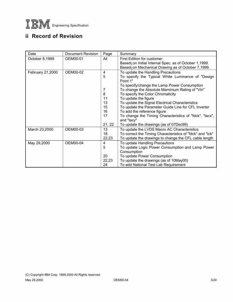
ii Record of Revision
To update Handling PrecautionsTo update Logic Power Consumption and Lamp PowerConsumptionTo update Power ConsumptionTo update the drawings (as of 10May00)To add National Test Lab Requirement
45
2022,2324
OEM00-04May 29,2000
To update the LVDS Macro AC CharacteristicsTo correct the Timing Characteristics of "fdck" and "tck"To update the drawings to change the CFL cable length
131822,23
OEM00-03March 23,2000
To update the Handling PrecautionsTo specify the Typical White Luminance of "DesignPoint 1"To specify/change the Lamp Power ConsumptionTo change the Absolute Mamimum Rating of "Vin"To specify the Color ChromaticityTo update the figureTo update the Signal Electrical CharacteristicsTo update the Parameter Guide Line for CFL InverterTo add the reference figureTo change the Timing Characteristics of "fdck", "tacx",and "tacy"To update the drawings (as of 07Dec99)
45
781113151617
21, 22
OEM00-02February 21,2000
First Edition for customer.Based on Initial Internal Spec. as of October 1,1999.Based on Mechanical Drawing as of October 7,1999.
AllOEM00-01October 8,1999SummaryPageDocument RevisionDate
Engineering Specification
(C) Copyright IBM Corp. 1999,2000 All Rights reserved.
May 29,2000 OEM00-04 3/24

1.0 Handling Precautions 1) Since front polarizer is easily damaged, pay attention not to scratch it. 2) Be sure to turn off power supply when inserting or disconnecting from input connector. 3) Wipe off water drop immediately. Long contact with water may cause discoloration or spots. 4) When the panel surface is soiled, wipe it with absorbent cotton or other soft cloth. 5) Since the panel is made of glass, it may break or crack if dropped or bumped on hard surface. 6) Since CMOS LSI is used in this module, take care of static electricity and insure human earth when handling. 7) Do not open nor modify the Module Assembly. 8) Do not press the reflector sheet at the back of the module to any directions. 9) Do not stick the adhesive tape on the reflector sheet at the back of the module. 10) In case if a Module has to be put back into the packing container slot after once it was taken out from the container, do not press the center of the CFL Reflector edge. Instead, press at the far ends of the CFL Reflector edge softly. Otherwise the TFT Module may be damaged. 11) At the insertion or removal of the Signal Interface Connector, be sure not to rotate nor tilt the Interface Connector of the TFT Module. 12) After installation of the TFT Module into an enclosure ( Notebook PC Bezel, for example), do not twist nor bent the TFT Module even momentary. At designing the enclosure, it should be taken into consideration that no bending/twisting forces are applied to the TFT Module from outside. Otherwise the TFT Module may be damaged. 13) The fluorescent lamp in the liquid crystal display (LCD) contains mercury. Do not put it in trash that is disposed of in landfills. Dispose of it as required by local ordinances or regulations. 14)Small amount of materials having no flammability grade is used in the LCD module. The LCD module should be supplied by power complied with requirements of Limited Power Source (2.11, IEC60950 or UL1950), or be applied exemption conditions of flammability requirements (4.4.3.3, IEC60950 or UL1950) in an end product. 15)The LCD module is designed so that the CFL in it is supplied by Limited Current Circuit (2.4, IEC60950 or UL1950). Do not connect the CFL in Hazardous Voltage Circuit.
The information contained herein may be changed without prior notice. It is thereforeadvisable to contact IBM before proceeding with the design of equipment incorporating thisproduct.
The information contained herein is presented only as a guide for the applications of ourproducts. No responsibility is assumed by IBM for any infringements of patents or other rightof the third partied which may result from its use. No license is granted by implication orotherwise under any patent or patent rights of IBM or others.
Engineering Specification
(C) Copyright IBM Corp. 1999,2000 All Rights reserved.
May 29,2000 OEM00-04 4/24
2.0 General DescriptionThis specification applies to the 12.1 inches Color TFT/LCD Module 'ITXG00'.This module is designed for a display unit of notebook style personal computer.The screen format and electrical interface are intended to support the XGA (1024(H) x 768(V))screen.Support color is native 262k colors ( RGB 6-bit data driver ).All input signals are LVDS interface compatible.This module does not contain a inverter card for backlight.
2.1 CharacteristicsThe following items are characteristics summary on the table under 25 ℃ condition:
0 to +50-20 to +60
Temperature Range (℃)OperatingStorage (Shipping)
Native 262K colors ( RGB 6-bit data driver )Support Color
6-bit digital video for each color R/G/B, 3 sync, Clock4 pairs LVDS
Electrical Interface
262(W) x 198(H) x 5.7(D) Typ.Physical Size [mm]370 Typ.(w/o Inverter)Weight [grams]
2.0 Typ.3.5 Typ.
Lamp Power Consumption [watt]Design Point 1:(ICFL=3.5mA)Design Point 2:(ICFL=6.5mA)
1.3 Typ.Logic Power Consumption[watt](VDD line)
+3.3 Typ.Nominal Input Voltage [Volt] VDD
30 Typ., 50 Max.(each) Optical Rise Time/Fall Time [msec]
200 : 1 Typ.Contrast Ratio
90 Typ.(Center), 80 Typ (5 points average)150 Typ.(Center), 140 Typ.(5 points average)
Typical White Luminance [cd/㎡]Design Point 1:(ICFL=3.5mA)Design Point 2:(ICFL=6.5mA)
Normally WhiteDisplay Mode
R.G.B. Vertical StripePixel Arrangement
0.240(per one triad x3) x 0.240Pixel Pitch [mm]
1024(x3) x 768Pixels H x V
245.76(H) x 184.32(V)Active Area [mm]
307.2 (12.1")Screen Diagonal [mm]
SPECIFICATIONSITEMS
Engineering Specification
(C) Copyright IBM Corp. 1999,2000 All Rights reserved.
May 29,2000 OEM00-04 5/24

2.2 Functional Block DiagramThe following diagram shows the functional block of the 12.1 inches Color TFT/LCD Module:
TFT ARRAY/CELL
VDD
LCDController
LCD DRIVECARD
Backlight Unit
1024(R/G/B) x 768
GND
DC-DCConverterRef circuit
Y-Driver
X-Driver
<4 pairs LVDS>
RxIN1
RxIN0
RxIN2
RxCLKIN
LampConnector
JST BHSR-02VS-1
JAE FI-XB20S-HF10Mating JAE FI-X20M
Mating JST SM02B-BHSS-1-TB
Engineering Specification
(C) Copyright IBM Corp. 1999,2000 All Rights reserved.
May 29,2000 OEM00-04 6/24
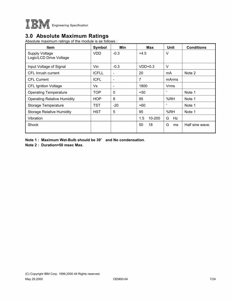
3.0 Absolute Maximum RatingsAbsolute maximum ratings of the module is as follows :
Half sine wave.G ms50 18Shock
G Hz1.5 10-200VibrationNote 1%RH955HSTStorage Relative Humidity
Note 1℃+60-20TSTStorage Temperature
Note 1%RH958HOPOperating Relative Humidity
Note 1℃+500TOPOperating TemperatureVrms1800-VsCFL Ignition Voltage
mArms7-ICFLCFL Current
Note 2mA20-ICFLLCFL Inrush currentVVDD+0.3-0.3VinInput Voltage of Signal
V+4.5-0.3VDDSupply Voltage Logic/LCD Drive Voltage
Conditions Unit Max MinSymbol Item
Note 1 : Maximum Wet-Bulb should be 39℃℃℃℃ and No condensation.Note 2 : Duration=50 msec Max.
Engineering Specification
(C) Copyright IBM Corp. 1999,2000 All Rights reserved.
May 29,2000 OEM00-04 7/24

4.0 Optical CharacteristicsThe optical characteristics are measured under stable conditions as follows under 25℃ condition:
150Center
1405 pointsaverage
White Luminance(cd/㎡) CFL 6.5mA
-0.329White y-0.313White x-0.124Blue y-0.158Blue x-0.554Green y-0.310Green x(CIE)-0.338Red yChromaticity-0.577Red xColor
50(Max)30Falling(ms)50(Max)30RisingResponse Time-200Contrast ratio
--
1530
Vertical (Upper)K 10 (Lower)K:Contrast Ratio
--
4040
Horizontal (Right) K 10 (Left)
Viewing Angle (Degrees)
NoteTyp.SpecificationConditionsItem
Engineering Specification
(C) Copyright IBM Corp. 1999,2000 All Rights reserved.
May 29,2000 OEM00-04 8/24

5.0 Signal Interface5.1 ConnectorsPhysical interface is described as for the connector on module.These connectors are capable of accommodating the following signals and will be following components.
FI-X20MMating Type / Part Number
FI-XB20S-HF10Type / Part Number
JAEManufacturer
For Signal ConnectorConnector Name / Designation
SM02B-BHSS-1-TBMating Type / Part Number
BHSR-02VS-1Type / Part Number
JSTManufacturer
For Lamp ConnectorConnector Name / Designation
5.2 Signal Pin
GND21GND11
GND20RxIN1+10
Reserved19RxIN1-9
Reserved18GND8
GND17RxIN0+7
RxCLKIN+16RxIN0-6
RxCLKIN-15GND5
GND14GND4
RxIN2+13VDD3
RxIN2-12VDD2
SignalPin#SignalPin#
Note: Pin# 1 and 22 are connected to FG. Pin#s of mating connector are from #2 to #21.
Engineering Specification
(C) Copyright IBM Corp. 1999,2000 All Rights reserved.
May 29,2000 OEM00-04 9/24

5.3 Signal Description
The module uses a LVDS compatible receiver. LVDS is a differential signal technology for LCD interface and highspeed data transfer device. Transmitter shall be SN75LVDS84(negative edge sampling) or compatible.
GroundGND
+3.3V Power SupplyVDD
LVDS differential clock inputRxCLKIN+, RxCLKIN-
LVDS differential data input (Blue2-Blue5, HSync, VSync, DSPTMG)RxIN2+, RxIN2-
LVDS differential data input (Green1-Green5,Blue0-Blue1)RxIN1+, RxIN1-
LVDS differential data input (Red0-Red5, Green0)RxIN0+, RxIN0-
DescriptionSignal Name
Note: Input signals shall be low or Hi-Z state when VDD is off.
Engineering Specification
(C) Copyright IBM Corp. 1999,2000 All Rights reserved.
May 29,2000 OEM00-04 10/24

Internal circuit of LVDS inputs are as follows:
R
R
R
R
SN75LVDS86 Compat ib leSignal Input
Pin No.
RxIN0+
RxIN0-
RxIN1+
RxIN1-
RxIN2+
RxIN2-
RxCKLIN+
RxCLKIN-
6
9
10
12
13
15
16
7
+Red0+Red1+Red2+Red3+Red4+Red5+Green0+Green1+Green2+Green3+Green4+Green5+Blue0+Blue1+Blue2+Blue3+Blue4+Blue5HSYNCVSYNC
DSPTMG-DTCLK
The module uses a 100ohm resistor between positive and negative data lines of each receiver input.
Engineering Specification
(C) Copyright IBM Corp. 1999,2000 All Rights reserved.
May 29,2000 OEM00-04 11/24

The signal is synchronized to -DTCLK .Horizontal SyncHSYNCThe signal is synchronized to -DTCLK .Vertical SyncVSYNC
This signal is strobed at the falling edge of -DTCLK. Whenthe signal is high, the pixel data shall be valid to bedisplayed.
Display TimingDSPTMG
The typical frequency is 65.0 MHz. The signal is used tostrobe the pixel data and DSPTMG signals. All pixel datashall be valid at the falling edge when the DSPTMG signalis high.
Data Clock -DTCLK
Blue-pixel DataEach blue pixel's brightness data consists of these 6 bitspixel data.
Blue Data 5 (MSB)Blue Data 4Blue Data 3Blue Data 2Blue Data 1Blue Data 0 (LSB)
Blue-pixel Data
+BLUE 5+BLUE 4+BLUE 3+BLUE 2+BLUE 1+BLUE 0
Green-pixel DataEach green pixel's brightness data consists of these 6 bitspixel data.
Green Data 5 (MSB)Green Data 4Green Data 3Green Data 2Green Data 1Green Data 0 (LSB)
Green-pixel Data
+GREEN 5+GREEN 4+GREEN 3+GREEN 2+GREEN 1+GREEN 0
Red-pixel DataEach red pixel's brightness data consists of these 6 bitspixel data.
Red Data 5 (MSB)Red Data 4Red Data 3Red Data 2Red Data 1 Red Data 0 (LSB)
Red-pixel Data
+RED5+RED4+RED3+RED2+RED1+RED0
DescriptionSIGNAL NAME
Note: Output signals from any system shall be low or Hi-Z state when VDD is off.
Engineering Specification
(C) Copyright IBM Corp. 1999,2000 All Rights reserved.
May 29,2000 OEM00-04 12/24

5.4 Signal Electrical Characteristics
Input signals shall be low or Hi-Z state when VDD is off.It is recommended to refer the specifications of SN75LVDS86DGG(Texas Instruments) in detail.
Signal electrical characteristics are as follows;
mV50-50Vth-Vtl=200mVdVcmV1.51.21.0Vth-Vtl=200mVVcm
mV50-100Differential Input High Voltage (Vcm=+1.2V)
Vtl
mV10050Differential Input High Voltage (Vcm=+1.2V)
Vth
unitMaxTypMinConditionParameter
LVDS Macro AC characteristics are as follows:
Note[ps/clk]20TCJavgCycle Modulation Rate[ps]150-150TCCJMCycle-to-cycle Jitter
[ps]600ThdData Hold TimeFc=65MHz, Jitter<50ps,Vth-Vtl=200mV,Vcm=1.2V, Delta Vcm=0
[ps]600TsuData Setup Time[ms]10TpllPLL Lock Time[ns]20.0015.3814.93TcCycle Time
[MHz]676550FcClock Frequency
ConditionsunitMaxTypMinSymbol
Note: This specification defines maximum average cycle modulation rate in peak-to-peak transition within any100 clock cycles. This specification is applied only if input clock peak jitter within any 100 clock cycles isgreater than 300ps.
Input Clock
Input Data
Tsu Thd
Tc
Engineering Specification
(C) Copyright IBM Corp. 1999,2000 All Rights reserved.
May 29,2000 OEM00-04 13/24

5.5 Signal for Lamp connector
Lamp Low Voltage 2
Lamp High Voltage1
Signal NamePin #
Engineering Specification
(C) Copyright IBM Corp. 1999,2000 All Rights reserved.
May 29,2000 OEM00-04 14/24

6.0 Pixel Format Image
Following figure shows the relationship of the input signals and LCD pixel format image.
0 1 1022 1023
1st Line
768th Line
RGB RGBRGB
RGBRGB RGBRGB
RGB
Engineering Specification
(C) Copyright IBM Corp. 1999,2000 All Rights reserved.
May 29,2000 OEM00-04 15/24

7.0 Parameter Guide Line for CFL Inverter
(Ta=25℃)Note 2
W-3.541.96-CFL Power consumption(PCFL)
(Ta=25℃)Note 2
Vrms-545560-CFL Voltage (Reference)(VCFL)
(Ta= 0℃)
Note 3
Vrms---1,250CFL Ignition Voltage(Vs)
(Ta=25℃)Note 1
KHz60424240CFL Frequency(FCFL)
(Ta=25℃)Note 4
mArms6.56.53.52.5CFL current(ICFL)
(Ta=25℃)cd/㎡-150140
9080
-White Luminancecenter5 points average
CONDITIONUNITSMAXDP-2DP-1MINPARAMETER
Note 1: CFL discharge frequency should be carefully determined to avoid interference between inverter and TFTLCD.
Note 2: Calculated value for reference (ICFL x VCFL = PCFL).Note 3: CFL inverter should be able to give out a power that has a generating capacity of over 1,250 voltage. Lamp units need 1,250 voltage minimum for ignition.Note 4: It should be employed the inverter whitch has "Duty Dimming", if ICFL is less than 4 mA.Note 5: DP-1 and DP-2 are IBM recommended Design Points. *1 All of characteristics listed are measured under the condition using the IBM Test inverter. *2 In case of using an inverter other than listed, it is recommended to check the inverter carefully. Sometimes, interfering noise stripes appear on the screen, and substandard luminance or flicker at low power may happen. *3 In designing an inverter, it is suggested to check safety circuit very carefully. Impedance of CFL, for instance, becomes more than 1 [M ohm] when CFL is damaged. *4 Generally, CFL has some amount of delay time after applying kick-off voltage. It is recommended to keep on applying kick-off voltage for 1 [Sec] until discharge. *5 CFL discharge frequency must be carefully chosen so as not to produce interfering noise stripes on the screen. *6 Reducing CFL current increases CFL discharge voltage and generally increases CFL discharge frequency. So all the parameters of an inverter should be carefully designed so as not to produce too much leakage current from high-voltage output of the inverter.
Engineering Specification
(C) Copyright IBM Corp. 1999,2000 All Rights reserved.
May 29,2000 OEM00-04 16/24
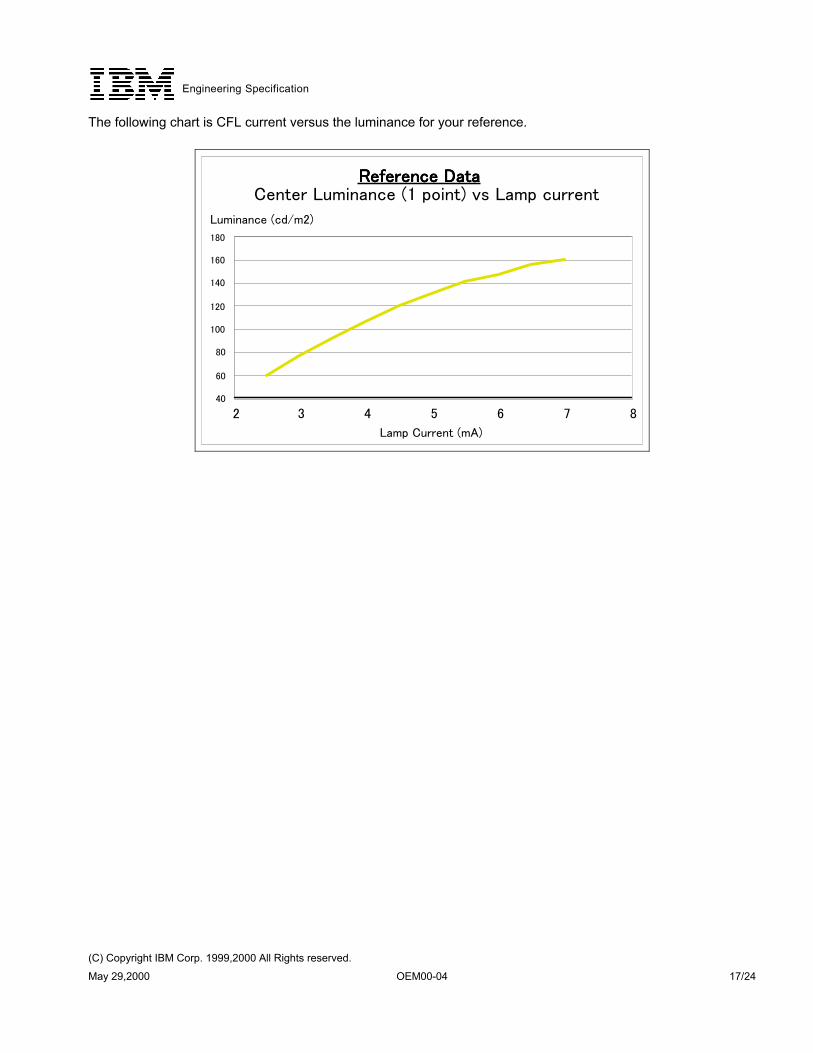
The following chart is CFL current versus the luminance for your reference.
2 3 4 5 6 7 8
Lamp Current (mA)
40
60
80
100
120
140
160
180
Luminance (cd/m2)
Reference DataReference DataReference DataReference DataCenter Luminance (1 point) vs Lamp current
Engineering Specification
(C) Copyright IBM Corp. 1999,2000 All Rights reserved.
May 29,2000 OEM00-04 17/24
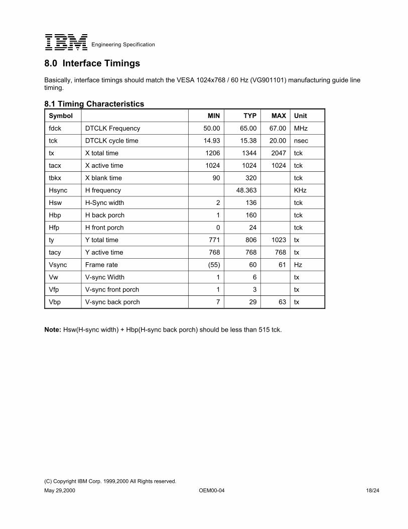
8.0 Interface Timings Basically, interface timings should match the VESA 1024x768 / 60 Hz (VG901101) manufacturing guide linetiming.
8.1 Timing Characteristics
tx63297V-sync back porchVbp
tx31V-sync front porchVfp
tx61V-sync WidthVw
Hz6160(55)Frame rateVsync
tx768768768Y active timetacy
tx1023806771Y total timety
tck240H front porchHfp
tck1601H back porchHbp
tck1362H-Sync widthHsw
KHz48.363H frequencyHsync
tck32090X blank timetbkx
tck102410241024X active timetacx
tck204713441206X total timetx
nsec20.0015.3814.93DTCLK cycle timetck
MHz67.0065.0050.00DTCLK Frequencyfdck
UnitMAXTYPMINSymbol
Note: Hsw(H-sync width) + Hbp(H-sync back porch) should be less than 515 tck.
Engineering Specification
(C) Copyright IBM Corp. 1999,2000 All Rights reserved.
May 29,2000 OEM00-04 18/24
8.2 Timing Definition
1344 dot
136 dot
160 dot24 dot
1024 dot
H-Sync
DSPTMG
38H
3H 29H
6H
768H
V-Sync
DSPTMG
Engineering Specification
(C) Copyright IBM Corp. 1999,2000 All Rights reserved.
May 29,2000 OEM00-04 19/24
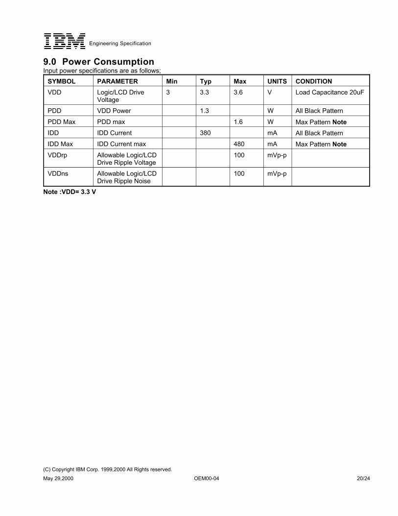
9.0 Power ConsumptionInput power specifications are as follows;
mVp-p100Allowable Logic/LCDDrive Ripple Noise
VDDns
mVp-p100Allowable Logic/LCDDrive Ripple Voltage
VDDrpMax Pattern NotemA480IDD Current maxIDD MaxAll Black Pattern mA380IDD Current IDD Max Pattern Note W1.6PDD maxPDD Max
All Black PatternW1.3VDD PowerPDD
Load Capacitance 20uFV3.63.33Logic/LCD DriveVoltage
VDDCONDITIONUNITSMaxTypMinPARAMETERSYMBOL
Note :VDD= 3.3 V
Engineering Specification
(C) Copyright IBM Corp. 1999,2000 All Rights reserved.
May 29,2000 OEM00-04 20/24

10.0 Power ON/OFF SequenceVDD power and lamp on/off sequence is as follows. Interface signals are also shown in the chart. Signals fromany system shall be Hi-Z state or low level when VDD is off.
90%
10%
10% 10%
90%
0.1ms min.
0 min. 0 min.
0 V
0 V
VDD
Signals
10% 10%
200ms min. 0 min.
0 V
Lamp On
10% 10%
30ms max.
30ms min.
Engineering Specification
(C) Copyright IBM Corp. 1999,2000 All Rights reserved.
May 29,2000 OEM00-04 21/24

11.0 Mechanical Characteristics
Engineering Specification
(C) Copyright IBM Corp. 1999,2000 All Rights reserved.
May 29,2000 OEM00-04 22/24

Engineering Specification
(C) Copyright IBM Corp. 1999,2000 All Rights reserved.
May 29,2000 OEM00-04 23/24
12.0 National Test Lab Requirement
The display module satisfied all requirements for compliance to UL 1950, 3rd Edition U.S.A. Information Technology Equipment
****** End Of Page ******
Engineering Specification
(C) Copyright IBM Corp. 1999,2000 All Rights reserved.
May 29,2000 OEM00-04 24/24


![2017 iFactory SRP Brochure SRP-FEC220 - Advantechadvcloudfiles.advantech.com/ecatalog/2017/01251022.pdf · [201] 12.1” XGA Ind. Monitor w/ Resistive TS ... RAM, 32G eMMC Storage,](https://static.fdocuments.us/doc/165x107/5ad0fa5b7f8b9a92258b8142/2017-ifactory-srp-brochure-srp-fec220-ad-201-121-xga-ind-monitor-w-resistive.jpg)