Energy Efficient High Data Rate RF-DAC based PAM...
52
Energy Efficient High Data Rate RF-DAC based PAM Modulator A MMIC solution using an InP-based DHBT-process at Mil- limeterwave Band Master’s thesis in Wireless, Photonics and Space Engineering FRIDA STRÖMBECK Department of Microtechnology and Nanoscience, MC2 CHALMERS UNIVERSITY OF TECHNOLOGY Gothenburg, Sweden 2018
Transcript of Energy Efficient High Data Rate RF-DAC based PAM...

Energy Efficient High Data RateRF-DAC based PAM ModulatorA MMIC solution using an InP-based DHBT-process at Mil-limeterwave Band
Master’s thesis in Wireless, Photonics and Space Engineering
FRIDA STRÖMBECK
Department of Microtechnology and Nanoscience, MC2CHALMERS UNIVERSITY OF TECHNOLOGYGothenburg, Sweden 2018

Master’s thesis 2018
Energy Efficient High Data Rate RF-DAC basedPAM Modulator
A MMIC solution using an InP-based DHBT-process atMillimeterwave Band
FRIDA STRÖMBECK
Department of Microtechnology and Nanoscience, MC2Microwave Electronics Laboratory
Chalmers University of TechnologyGothenburg, Sweden 2018

Energy Efficient High Data Rate RF-DAC based PAM ModulatorA MMIC solution using an InP-based DHBT-process at Millimeterwave BandFRIDA STRÖMBECK
© FRIDA STRÖMBECK, 2018.
Supervisor: Zhongxia Simon He, Herbert Zirath, Microwave Electronics LaboratoryExaminer: Herbert Zirath, Microwave Electronics Laboratory
Master’s Thesis 2018Department of Microtechnology and Nanoscience, MC2Microwave Electronics LaboratoryChalmers University of TechnologySE-412 96 GothenburgTelephone +46 31 772 1000
Typeset in LATEXPrinted by [Name of printing company]Gothenburg, Sweden 2018
iv

Energy Efficient High Data Rate RF-DAC based PAM ModulatorA MMIC solution using an InP-based DHBT-process at Millimeterwave BandFRIDA STRÖMBECKDepartment of Microtechnology and Nanoscience, MC2Chalmers University of Technology
AbstractTo achieve a high-data rate wireless communication system with PAM-4 modulationis tested in this project. A MMIC solution is developed and fabricated with TeledyneScientific Instruments, US, in their 250nm InP DHBT-process with fmax =650GHz.The simulated system consists of a RF-DAC, a PA, transmitter and receiver antennawith 40dBi gain, an LNA, a VGA and a PD. ADS simulation shows that the systemlooks promising. The critical part in the system is the RF-DAC based modulator,which is why two different solutions are tested and evaluated.The modulators aredesigned for an LO frequency of 70GHz, though the plan is to double the frequencywhen the function of the chosen RF-DAC is confirmed. The reason to not designfor an LO frequency of 140GHz straight away is to simplify the testing process.Symbol rate for one of the fabricated modulators is tested and confirmed to supporta 40Gbps transmission with a BER of 3.7× 10⁻⁶, and the energy efficiency is betterthan 1.2pJ/bit.
Keywords: Energy efficiency, High data rate, Pulse Amplitude Modulation, InP,RF-DAC, DHBT, MMIC, Internet of Things
v


AcknowledgementsA special thanks to Simon He and Herbert Zirath for inspiration, support and pa-tience.I would also like to thank the Technology Department, Teledyne Scientific Company,for fabrication of the MMICs.Finally, I would like to thank Microwave Electronics Laboratory, Department ofMicrotechnology and Nanoscience, MC2, Chalmers University of Technology forgiving me this opportunity.
Frida Strömbeck, Gothenburg, March 2018
vii


Contents
List of Figures xi
List of Tables xiii
1 Introduction 11.1 Background . . . . . . . . . . . . . . . . . . . . . . . . . . . . . . . . 11.2 Application . . . . . . . . . . . . . . . . . . . . . . . . . . . . . . . . 11.3 Problem statement and description . . . . . . . . . . . . . . . . . . . 21.4 Purpose and Aim . . . . . . . . . . . . . . . . . . . . . . . . . . . . . 21.5 Thesis outline . . . . . . . . . . . . . . . . . . . . . . . . . . . . . . . 3
2 Theoretical Background 52.1 Typical Setup . . . . . . . . . . . . . . . . . . . . . . . . . . . . . . . 52.2 Choice of Modulation . . . . . . . . . . . . . . . . . . . . . . . . . . . 6
2.2.1 Pulse Amplitude Modulation . . . . . . . . . . . . . . . . . . 72.3 Overview of System . . . . . . . . . . . . . . . . . . . . . . . . . . . . 72.4 Link Budget . . . . . . . . . . . . . . . . . . . . . . . . . . . . . . . . 92.5 Critical Component and Previous work . . . . . . . . . . . . . . . . . 10
2.5.1 RF-DAC . . . . . . . . . . . . . . . . . . . . . . . . . . . . . . 11
3 Circuit Design 133.1 Technology . . . . . . . . . . . . . . . . . . . . . . . . . . . . . . . . 133.2 Design Flow . . . . . . . . . . . . . . . . . . . . . . . . . . . . . . . . 163.3 RF-DAC . . . . . . . . . . . . . . . . . . . . . . . . . . . . . . . . . . 16
3.3.1 Design Concept . . . . . . . . . . . . . . . . . . . . . . . . . . 163.3.2 Schematic . . . . . . . . . . . . . . . . . . . . . . . . . . . . . 213.3.3 Circuit Layout . . . . . . . . . . . . . . . . . . . . . . . . . . 23
4 Results 254.1 V1:PAM-4 RF-DAC (differential pair) . . . . . . . . . . . . . . . . . . 25
4.1.1 Frequency Domain Measurement . . . . . . . . . . . . . . . . 254.1.2 Time Domain Measurement . . . . . . . . . . . . . . . . . . . 27
4.2 V2:PAM-4 RF-DAC (cascode) . . . . . . . . . . . . . . . . . . . . . . 294.2.1 Frequency Domain Simulation . . . . . . . . . . . . . . . . . . 294.2.2 Time Domain Simulation . . . . . . . . . . . . . . . . . . . . . 30
4.3 Specifications for the Circuits . . . . . . . . . . . . . . . . . . . . . . 32
ix

Contents
5 Discussion and Conclusion 35
Bibliography 37
x
List of Figures
2.1 A basic transmitter and receiver. . . . . . . . . . . . . . . . . . . . . 52.2 Symbol error probability for coherent M-PAM. . . . . . . . . . . . . . 82.3 The parameters for the transmitter and receiver link. . . . . . . . . . 82.4 The suggested transmitter and receiver link with a center frequency
of 140GHz. . . . . . . . . . . . . . . . . . . . . . . . . . . . . . . . . 9
3.1 Representative cross-section of TSC250 IC technology. Drawing isnot to scale. Credit: Teledyne Scientific Company . . . . . . . . . . . 14
3.2 Estimated safe operating area for 250nm HBT devices in common-emitter configuration. The current density is given by JE = IC
(0.25×Emitter length) .Credit: Teledyne Scientific Company . . . . . . . . . . . . . . . . . . 14
3.3 The design steps in ADS. . . . . . . . . . . . . . . . . . . . . . . . . . 163.4 The most simple form of PAM is OOK. A transmitted signal repre-
sents "1", while no transmitted signal is "0". . . . . . . . . . . . . . . 173.5 The schematic of one switch with the differential pair solution. . . . . 193.6 The schematic of one switch with the cascode solution. . . . . . . . . 203.7 The full schematic of the differential pair RF-DAC. The value of each
component can be seen in table 3.1. . . . . . . . . . . . . . . . . . . . 213.8 The full schematic of the cascode RF-DAC. The value of each com-
ponent can be seen in table 3.2. . . . . . . . . . . . . . . . . . . . . . 223.9 The final layout of the differential PAM-4 RF-DAC. The size is 800x800µm. 233.10 The final layout of the cascode PAM-4 RF-DAC. The size is 800x800µm. 24
4.1 Measured output power at different frequencies with different digitalinput. The dotted lines are simulated values. It can be seen that thesimulated values have a wider 3-dB bandwidth compared to the realmeasurements. This could be explained by the limited bandwidth ofthe probes used during the measurements. . . . . . . . . . . . . . . . 26
4.2 Measured input and output matching at LO and RF port. . . . . . . 264.3 Simulated output power for different data input voltages of the MSB,
with different input power (LO). The LSB is set to 0 V and the LOfrequency is 75 GHz. . . . . . . . . . . . . . . . . . . . . . . . . . . . 27
4.4 Measured 20 Gbps ASK modulated waveform in time-domain at 50GHz center frequency . . . . . . . . . . . . . . . . . . . . . . . . . . . 28
4.5 Received constellation diagram after demodulation using ASK. . . . . 284.6 Received constellation diagram after demodulation using PAM4. . . . 28
xi

List of Figures
4.7 The RF output power for different values of LO input power for the"cascode" RF-DAC. . . . . . . . . . . . . . . . . . . . . . . . . . . . 29
4.8 Simulated output power at different frequencies with different digitalinput for the "cascode" RF-DAC. The LO input power is 5dBm inthis simulation. . . . . . . . . . . . . . . . . . . . . . . . . . . . . . . 30
4.9 Simulated input and output matching at LO and RF port for the"cascode" RF-DAC. . . . . . . . . . . . . . . . . . . . . . . . . . . . . 30
4.10 Simulated waveform with 30Gbps data rate transmission using OOKmodulation for the "cascode" RF-DAC. The LO frequency is 70GHzand the LO input power is 5dBm. . . . . . . . . . . . . . . . . . . . . 31
4.11 Simulated waveform with 20Gbd data rate transmission using PAM-4modulation for the "cascode" RF-DAC. The LO frequency is 70GHzand the LO input power is 5dBm. . . . . . . . . . . . . . . . . . . . . 31
4.12 Photo of the fabricated RF-DAC (V1). The chip size is 800µm x800µm. . . . . . . . . . . . . . . . . . . . . . . . . . . . . . . . . . . . 32
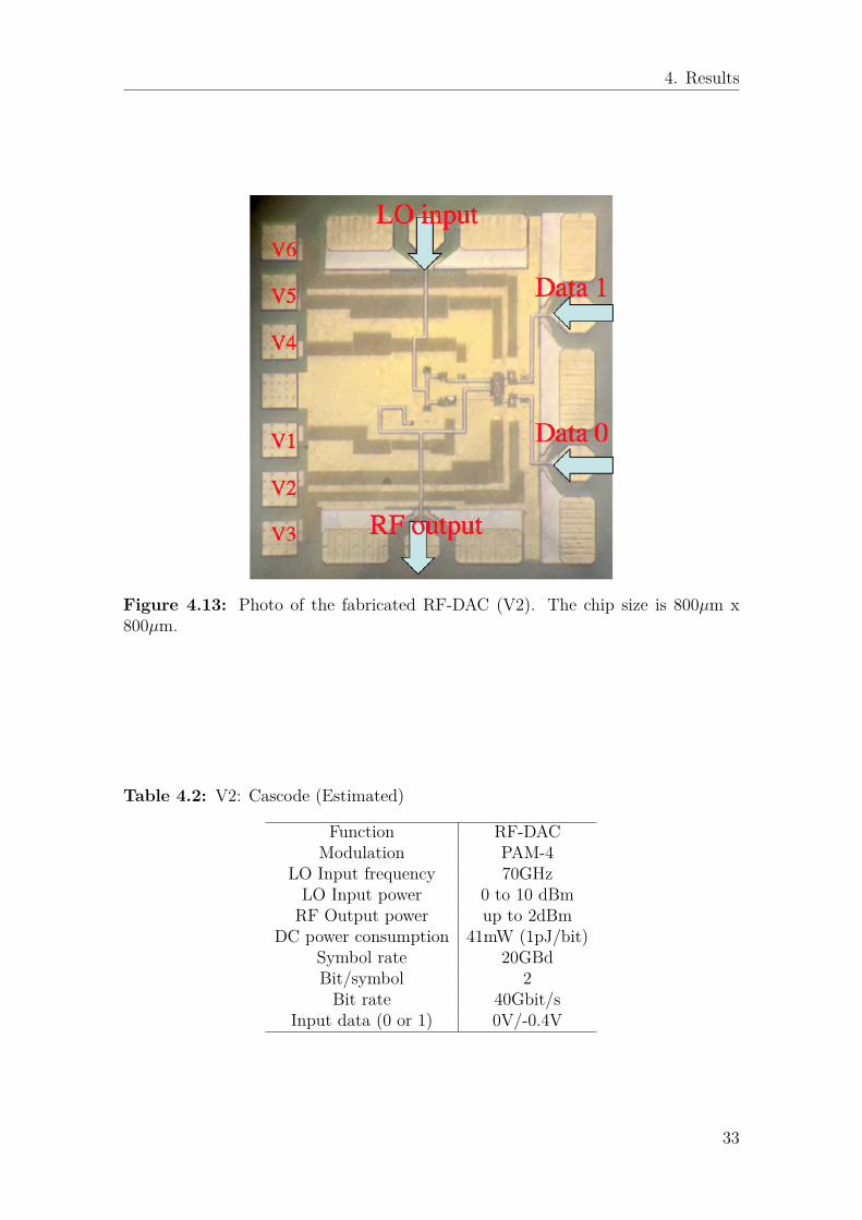
4.13 Photo of the fabricated RF-DAC (V2). The chip size is 800µm x800µm. . . . . . . . . . . . . . . . . . . . . . . . . . . . . . . . . . . . 33
xii

List of Tables
2.1 Link Budget-(from transmitter to receiver) . . . . . . . . . . . . . . . 102.2 Link Budget-(in receiver) . . . . . . . . . . . . . . . . . . . . . . . . . 102.3 Comparison with similar work in D-band (transmitter & receiver) . . 102.4 Comparison with similar work in E-band (transmitter & receiver) . . 112.5 Comparison with similar work (Modulators) . . . . . . . . . . . . . . 11
3.1 The values for each component in figure 3.7. . . . . . . . . . . . . . . 213.2 The values for each component in figure 3.8. . . . . . . . . . . . . . . 22
4.1 V1: Differential pair . . . . . . . . . . . . . . . . . . . . . . . . . . . 324.2 V2: Cascode (Estimated) . . . . . . . . . . . . . . . . . . . . . . . . . 33
xiii

List of Tables
xiv

1Introduction
In today’s fast paced world we are striving for solutions to transfer information fasterand faster. For a sustainable future, power efficiency is key. However, there are fewwilling to sacrifice performance to achieve higher power efficiency. It is therefore ahigh priority to develop systems that can compete in speed and performance, yethave a low power consumption.
1.1 BackgroundThe exchange of information with someone that is distant, is known as telecommu-nications. The most primitive form of telecommunications is using smoke signals.Before telecommunications messages had to be sent by a courier.The history went from mechanical telegraphs in 1794, to transmissions using copperwires in 1837. Heinrich Hertz used electromagnetic waves in 1886. Optical fibercommunication over a distance came in 1973.[1] Nowadays means for telecommuni-cation is a given, and most people have access to Internet 24/7.Both wireless communication using antennas and optical fiber communication areused today, because both systems have different advantages and drawbacks. A fiberoptic system can reach far, but a wireless system is much more flexible.The flexibility of wireless systems combined with smaller devices and antennas makeswireless communication interesting for the future’s new short range applications.
1.2 ApplicationThe primary use of wireless communication is telecommunication, such as mobilephone networks, Wireless Local Area Network (WLAN), commonly referred as WiFi,as well as mobile satellite communication for areas where WiFi is unavailable.Wireless can also be used to replace a cable or fiber for short distances. Thatapplication is called cordless. Headphones, printers, keyboards and so on can beconnected to your phone or computer etc.All RADAR(Radio Detection and Ranging) systems rely on wireless signals. Auto-matic breaking function, parking assistance and automatic car following are only afew of the applications for cars for example.There are also medical technologies using wireless communication, such as mobilebody area networks (MBAN), for monitoring the patients’ health.Wireless transmission of video is also a common application. The higher the qualityof the video, the more bits need to be transmitted per second.
1
1. Introduction
Wireless power transfer (WPT) is the application where energy is transmitted froma power source to a device without the use of a wire. Examples include electricaltrains, chargers for electrical tooth brushes or smart watches, and smart cards suchas SIM cards and credit cards.It is clear that high data rate connectivity even at a small distance is urgentlyneeded. Since most mobile devices are battery driven, power consumption becomesa major consideration. Further more, a high data rate wireless link with decreasethe transmission time, thus reduce the on-time of the transceiver which enables alonger lifetime of the device.
1.3 Problem statement and descriptionWhat limits the symbol rate of the transmission is the response time of the compo-nents making up the transmitter/receiver as well as the noise in the channel. Thereis a theoretical limit of the maximum bit rate that can be transferred. In practise,the performance is always lower. The limit is given by Shannon’s theorem;[2]
C = Blog2(1 + S
N) (1.1)
where C is the channel capacity, B is the bandwidth, S is the signal power and Nis the noise power.If the response time of the components is limited the data rate can be increased bytransferring more data per symbol. A common way to do this is to change the phaseof the signal in combination with the amplitude. The disadvantage of this solutionis that it requires synchronisation (carrier recovery) between the transmitter andthe receiver, so a large portion of the power consumption is spent on that. It alsorequires a more complicated circuit.In the circuits designed today there is a trade-off between a high data-rate and ahigh energy efficiency. The designs are usually optimised for only one of those.Transceivers that uses on-off keying(OOK) has many advantages, such as a low DCpower consumption and a small chip area due to its simplicity.[20] For cases whenthe bandwidth is not extremely limited as a result of frequency allocation, OOKtransceivers are cost efficient. There is one big downside; the low spectral efficiency.
1.4 Purpose and Aim
In this work, MMIC(Microwave Monolithic Integrated Circuit)-solutions for energyefficient, high data-rate wireless communication will be analysed and designed.A MMIC-process using InP(Indium Phosphide)-based DHBTs(Double Heterojunc-tion Bipolar Transistor) with fmax = 650GHz, and a back-end with 4 metal layerswill be used for the active and passive components.The process using InP-based DHBTs is chosen due to the wide bandwidth and highpower handling capability, as well as a low noise figure. The technology ideally suitedfor next generation millimeterwave, mixed-signal and digital integrated circuits.
2

1. Introduction
The transmitter is aimed to be designed in the frequency band 110-170 GHz, alsoknown as the D-band. It will be optimised for highest modulation bandwidth andRF-bandwidth, in other words aiming for the highest bit-rate. However, to verifythe function of the transmitter and simplify testing it will first be designed andfabricated for a frequency band around 70GHz (E-band).Important design parameters are RF-bandwidth, IF-bandwidth, noise figure, chip-area, bit-rate, energy-per-bit, and DC-power consumption.The suggested solution to limit the power consumption is to use Pulse AmplitudeModulation (PAM). In some cases (unipolar), no synchronisation between the trans-mitter and receiver is needed using this modulation technique. Further more, thedesign can be kept simple.The design is fabricated at Teledyne Scientific Instruments, US, in their 250nmDHBT-process with fmax =650GHz.
1.5 Thesis outlineFirst the theory of the development of the circuit will be presented. This includes adeeper explanation of pulse amplitude modulation, followed by an overview of thecircuit where the design parameters are established. A link budget of the system isthen estimated, as well as a comparison with previous similar work made by othersof the system and the critical components.The tools to create and simulate the performance of the circuits is reviewed as wellas the technology.The desired functions of the modulator is explained, and different solutions toachieve those qualities are presented.The results of this work includes the layouts of the circuits, the performance of thecircuits, and the final circuit specifications.A discussion of the similarities and differences between expected results, actualresults and results of others will follow. The methods and uncertainties will bereviewed and some future research ideas and possibilities for improvement will bepresented.The report will be wrapped up with a conclusion.
3

1. Introduction
4

2Theoretical Background
2.1 Typical SetupThe basic transmitter/receiver system consists of a modulator followed by a PowerAmplifier(PA) and an antenna. The receiver antenna is followed by a Low NoiseAmplifier(LNA), and a demodulator. A simple figure can be seen in figure 2.1.
Figure 2.1: A basic transmitter and receiver.
Friis’ transmission equation helps calculating the amount of power that gets trans-mitted from one antenna to the other.
Pr = GtGrPt
FSPL (2.1)
Pr is the received power, Pt is the transmitted power, Gt is the antenna gain of thetransmitting antenna, Gr is the antenna gain of the receiving antenna, and FSPLis the free space path loss. The free space path loss can be calculated using;
FSPL = (4πdfc
)2 (2.2)
where d is the distance, f is the frequency and c is the speed of light.[19] What limitsthe transmission is usually noise, both thermal noise from the receiver antenna andnoise that gets added inside the components.The thermal noise power at the input is given by;
N0 = kTB (2.3)
where k is Boltzmann’s constant, T is the temperature of the antenna (usually roomor outdoor temperature), and B is the bandwidth of the signal.[19]
5

2. Theoretical Background
Signal to noise ratio (SNR) is common measurement within wireless communica-tions. It is defined as;
SNR = Pin
N0= Eb
n0
Rb
B(2.4)
where N0 = n0B is the noise power and EbRb is the digital signal power. Furthermore, Rb
Bis the spectral efficiency.
The noise that is contributed by the component makes the SNR lower at the outputof said component. The change in SNR is defined as the noise figure (NF) of thecomponent.[19]
NF = SNRin
SNRout(2.5)
For a cascaded circuit the total noise figure is given by Friis’ formula for noise;
NF = F1 + F2 − 1G1
(2.6)
where F1 is the noise figure of the first component, G1 is the gain from the firstcomponent, and F2 is the noise figure from the second component.[19]The symbol error rate depends on the SNR. A higher SNR gives a smaller symbolerror rate.A symbol can contain one or many bits, depending on the spectral efficiency of themodulation format.
2.2 Choice of Modulation
The most commonly used modulation techniques are Frequency Shift Keying (FSK),Phase-Shift Keying (PSK), Amplitude Shift Keying (ASK) and Quadrature Ampli-tude Modulation (QAM). FSK is mostly used for amateur radio, caller ID andemergency broadcasts. The most common modulation using phase is QuadraturePhase Shift Keying (QPSK) that uses 4 different phases. When only 2 differentphases are used it is called Binary Phase-Shift Keying (BPSK). QPSK and BPSKhas the same bandwidth and bit error rate though, which makes QPSK the morepopular choice since it has a higher spectral efficiency.On-Off keying (OOK) is the most simple modulation based on amplitude shift key-ing. No carrier recovery is required, so the receiver (Rx) structure can be keptsimple. The drawback with OOK is the low spectral efficiency.QAM is a mix between amplitude and phase modulation. Spectral efficiency in-creases with the order of QAM, but higher SNR is needed to reach the same BER.QAM requires carrier recovery which means that it has to have a more complex Rxstructure.Pulse Amplitude Modulation (PAM) has the same benefits as OOK. It requires nocarrier recovery. The advantage that PAM has to OOK is that the spectral efficiencycan be higher. If 4 levels are used, 2 bits are transmitted, which is double that ofOOK.
6

2. Theoretical Background
2.2.1 Pulse Amplitude ModulationPulse Amplitude Modulation(PAM) can be either unipolar or bipolar. For a unipolarsignal all levels are non-negative, while a bipolar signal has evenly distributed levelswhere half of them are negative and half of them are positive. A bipolar signal usesa single side band, but requires carrier recovery. A unipolar signal can use both sidebands, and a simple power detector is sufficient to demodulate the signal. In thisproject unipolar PAM is used.The transmitted unipolar PAM signal over one symbol period (0 ≤ t ≤ T ) is givenby;
si(t) = Aig(t)sin(2πfct) (2.7)
where Ai = (i − 1)d, i = 1, 2, 3...M for unipolar M-PAM, d is the amplitude sepa-ration distance between different levels, g(t) is a real-valued pulse shaping function,and fc is the carrier frequency.The drawback with PAM is that it is sensitive to amplitude noise and requires ahigher SNR than frequency or phase modulation. [21] Low noise material is definitelya game changer when it comes to designing circuits for PAM.The symbol error probability for coherent bipolar M-PAM is given by;
Ps = 2(M − 1)M
Q(√
6γs
M2 − 1) (2.8)
where γs = Es
N0≈ Eb
N0Log2(M), Es is the average energy per symbol, and Q(
√2x) =
erfc(x)2 . Note that erfc is referring to the complementary error function.[22]
The symbol error probability for coherent unipolar M-PAM is given by;
Ps = 2(M − 1)M
Q(√
3γs
2M2 − 3M + 1) (2.9)
In figure 2.2 the symbol error probability for both unipolar and bipolar M-PAM isplotted. Unipolar PAM requires a higher signal to noise ratio, but requires a muchlower DC power consumption.[22]To achieve a symbol error probability below 10−5 the Eb/N0 ratio has to be largerthan 18dB for unipolar PAM-4. For unipolar PAM-8 it has to be larger than 23.5dB,so the difference is 5.5dB.
2.3 Overview of SystemWhen designing parts of a system, it is important to have an understanding of thesystem as a whole. It is from the analysis of the system, the requirements for eachpart can be estimated and established.System parameters to estimate:
• Antenna gain (Gt and Gr)• Output power from transmitter
• Noise temperature• Distance of transmission
7

2. Theoretical Background
Figure 2.2: Symbol error probability for coherent M-PAM.
Figure 2.3: The parameters for the transmitter and receiver link.
• LNA gain• Noise figure LNA
• VGA gainThe antennas that were to be used were already specified and have an antennagain of Gantenna = 40dBi. The noise temperature is based on room temperature(≈ 300K). The reason to include a variable gain amplifier (VGA) is to control howmuch power get to the power detector. Further more, the input power will varywith distance changes between transmitter and receiver. The free space path loss
8

2. Theoretical Background
(FSPL) is 135dB for 1000 meters and 115dB for 100 meters at 140GHz.The estimation of the LNA gain and noise figure were based on previous work [4].Their LNA had a 20dB gain and a noise figure of 9dB, which means that it shouldbe no problem designing one with a 30dB gain and maximum a 10dB noise figure,but possible to make smaller.The saturated output power of the power amplifier is based on previous work fromTeledyne Scientific Company [23], using the same technology. They achieve anoutput power of more than 19dBm, at 96-120GHz, with a power added efficiency(PAE) of approximately 20%. PAE is defined as;[24]
PAE = PRF,out − PRF,in
PDC(2.10)
Based on these estimations a link budget was done. See figure 2.4.
Figure 2.4: The suggested transmitter and receiver link with a center frequencyof 140GHz.
2.4 Link Budget
The link budget was done for both a center frequency of 140GHz and 70GHz. Thereason for 70GHz is to simplify the measurements of the circuit. A proof-of-conceptsystem will be created first in E-band (fc = 70GHz). When the functionality of thesystem is confirmed it will move up in frequency to D-band (fc = 140GHz).A signal to noise ratio of 19dB is theoretically enough for a low bit error rate usingunipolar PAM-4.
9

2. Theoretical Background
Table 2.1: Link Budget-(from transmitter to receiver)
Parameter fc = 140GHz fc = 70GHzPt 16dBm 16dBmGt 40dBi 40dBi
FSPL1km -135dB -129dBGr 40dBi 40dBiPr -39dBm -33dBm
(N0)40GHz,300K -98dB = -68dBm -71dBmSNRin 29dB 38dB
Table 2.2: Link Budget-(in receiver)
Parameter fc = 140GHz fc = 70GHzPr -39dBm 33dBm
(N0)40GHz,300K -98dB = -68dBm -71dBmGLNA 30dB 30dBNFLNA 10dB 10dBGVGA up to 25dB up to 25dBNFVGA 15dB 15dBPin,PD up to 16dBm up to 16dBmNFtot 10+(31.6-1)/1000 ≈ 10 = 10dB 10dB
SNRin,P D 29-10=19dB 38-10=28dB
2.5 Critical Component and Previous workThe critical component in the system is the RF-DAC. There are examples of previouswork that include amplifiers that achieve the performance (specified in the linkbudget) that is required for this work.In table 2.3 similar work of entire systems, D-band transmitter & receiver, is pre-sented. Work done in E-band can be seen in table 2.4.
Table 2.3: Comparison with similar work in D-band (transmitter & receiver)
Technology DC Power Size Gbps Energy Eff. Ref.Consumption (mW) (mm2) pJ/bit
40nm CMOS 98.4 0.32(Tx) 10 9.8 [3](17.9+80.5) 1.68(Rx)
250nm InP DHBT 357 1.17(Tx) 40 8.9 [4](165+192) 1.17(Rx)
250nm SiGe HBT 1100 0.45(Tx) 20 55 [5](610+490) 0.4(Rx)
250nm InP DHBT 357 1.17(Tx) 48 7.4 [6](165+192) 1.17(Rx)
40nm CMOS 209 0.44(Tx) 11 19 [7](77+132) 1.35(Rx)
10

2. Theoretical Background
Table 2.4: Comparison with similar work in E-band (transmitter & receiver)
Technology DC Power Size Gbps Energy Eff. Ref.Consumption (mW) (mm2) pJ/bit
130 SiGe BiCMOS 2000 9.7(Tx) > 1 NA [8](1350+650) 6.1(Rx)
2.5.1 RF-DAC
Table 2.5: Comparison with similar work (Modulators)
Technology Frequency Data Rate Energy Eff. Ref.(GHz) (Gbps) pJ/bit
50nm InGaAs HEMT 113 25 0.38 [9]65nm CMOS 77 12 0.75 [10]
0.25µm InP DHBT 100-150 14 3.35 [11]50nm mHEMT 87.8-98.2 18 5.6 [12]65nm CMOS 80 12 4.5 [13]65nm CMOS 57-66 11.5 1.1 [14]
11

2. Theoretical Background
12

3Circuit Design
The main concept of the system was to create a Radio Frequency-Digital to AnalogConverter (RF-DAC) that is using pulse amplitude modulation (PAM).All simulations were done by utilising Advanced Design System (ADS) that is pro-vided by Keysight EEsof Electronic Design Automation (EDA). More informationcan be found at their website [25].
3.1 Technology
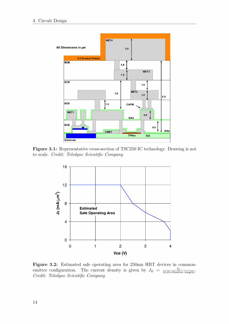
Teledyne Scientific Companies Indium Phosphide (InP) heterojunction bipolar tran-sistor (HBT) process TSC250 is an advanced bipolar process that relies on sub-micron transistor scaling to achieve state-of-the art device performance.[26] Devicesin the technology offer typical RF figures-of-merit (ft and fmax) of 350/600 GHzwhile maintaining a common-emitter breakdown voltage (BVCEO) of greater than4V. The wide bandwidth and high power handling capability of the devices makethe technology ideally suited for next generation millimeter-wave, mixed-signal anddigital integrated circuits.The technology has 4 metal layers, M1,M2,M3 and M4. The dielectric constant ofthe interlayer dielectric (BCB) is estimated to be εr = 2.7. A cross-section drawingcan be seen in figure 3.1.Thin-film resistors are formed on a thin layer of Silicon Oxide (SiO) that sits on theInP substrate. Metal-insulator-metal (MIM) capacitors are formed between M1 andthe capacitor metal (CAPM) with a 200nm Silicon Nitride (SiN) dielectric layer inbetween.Each layer has a maximum current density that cannot be exceeded. Metal 1 has4mA/µm, metal 2 and 3 has 5mA/µm, metal 4 has 15mA/µm and the thin-filmresistor has 1mA/µm. The VIAs connecting different layers also has limits for thecurrent.The design kit includes two types of transistors; standard devices, and single-sidedcollector contact devices. The single-sided collector device has a collector contacton only one side of the base mesa. This results in approximately a 2x increase inthe collector resistant, but reduces the footprint of the transistor by approximately30%. The estimated safe operating area for the devices can be seen in 3.2.Usually metal 1 or metal 2 is used as the ground layer. For this project metal 2 wasused as ground layer, while metal 1 was used for DC bias. That meant that RF andDC connections did not cross each others path or disturb each other.
13
3. Circuit Design
Figure 3.1: Representative cross-section of TSC250 IC technology. Drawing is notto scale. Credit: Teledyne Scientific Company
Figure 3.2: Estimated safe operating area for 250nm HBT devices in common-emitter configuration. The current density is given by JE = IC
(0.25×Emitter length) .Credit: Teledyne Scientific Company
14

3. Circuit Design
A design kit for TSC250 was available for ADS to simulate the predicted perfor-mance.
15

3. Circuit Design
3.2 Design FlowThe system has a few different parts with different functions.
1. RF-DAC2. PA3. Transmitting antenna4. Receiving antenna5. LNA6. VGA7. PD
The required performance for each part can be estimated through a link budget.ADS ptolomy simulation is also useful to get an idea about how different parametersaffect the system.
Figure 3.3: The design steps in ADS.
When the performance for each part was decided, the parts were designed one byone. The design steps of each part can be seen in figure 3.3.A schematic for each part was first decided. The parameters for the components ofeach part were changed to optimise the performance. The layouts were then createdusing the optimised schematics as a foundation. Input and output pads as wellas DC pads needs to be placed out in a way that minimises the area, but still ispractical for the testing and schematic. To see how the lines and components affecteach other EM-simulations were done. The layout then had to get adjusted andnew EM-simulations were done until a good performance was reached. To finalisethe layout, it also had to comply to all the design rules that Teledyne requiredto be fulfilled to be able to produce the MMIC. Each part was then placed in asystem simulation to see that the whole system worked together. To improve theperformance adjustments were done in the schematic or the optimisation, whichmeant that the other steps had to be made too.
3.3 RF-DAC
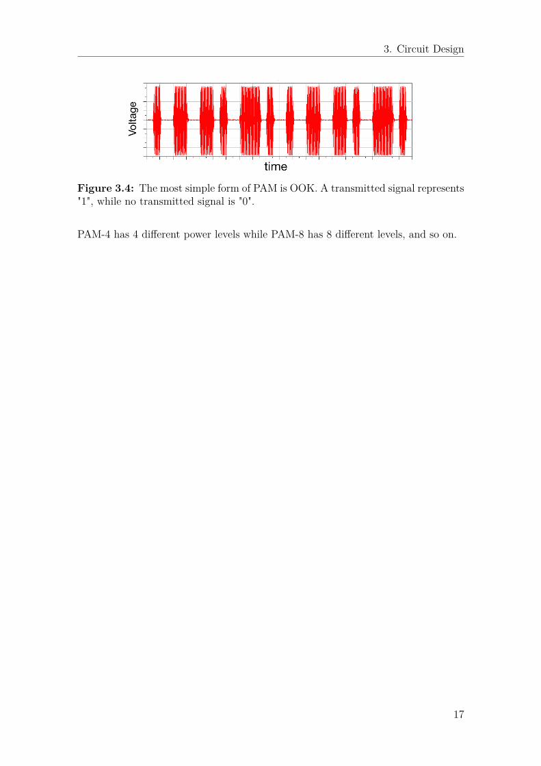
3.3.1 Design ConceptThe purpose of a RF-DAC(digital-to-analog converter) is to modulate the carrier sig-nal to represent the information that is to be transmitted. The modulation that waschosen for this project was Pulse Amplitude Modulation(PAM). The advantages ofunipolar PAM is that no synchronisation (signal recovery) between transmitter andreceiver is required. The most simple form of Pulse Amplitude Modulation(PAM)is On-Off-Keying(OOK). OOK can be seen in figure 3.4.
16
3. Circuit Design
Figure 3.4: The most simple form of PAM is OOK. A transmitted signal represents"1", while no transmitted signal is "0".
PAM-4 has 4 different power levels while PAM-8 has 8 different levels, and so on.
17

3. Circuit Design
The four different levels of PAM-4:
18

3. Circuit Design
The idea was to create two switches. One of them requires an output that is doublethat of the other. The data input port that gives the strongest output power is calledthe Most Significant Bit (MSB), while the weaker one is called the Least SignificantBit (LSB). The output signals need to be combined in phase, to avoid cancellingeach other. The input signal needs to be the same for both of them. The easiestway to achieve that is to divide one signal equally to supply both switches from thesame LO(Local Oscillator).For high-speed solutions current steering is the most commonly used technique tocreate an "On-Off"-switch. This can be done by using a differential pair.[17]One way to achieve the different power levels is to use a resistive ladder to combinethe output from the identical switches.[16] Another is to combine the output fromtwo different switches, one with an amplification that is double the other. To avoidlosing too much power (due to dissipation in the resistors) the second solution isused in this work.Two different schematics for switches were selected, one differential pair solution andone cascode solution. The schematics can be seen in figure 3.5 and 3.6. At the LOinput and the Data input an extra transistor stage was added to work as a buffer,a so called emitter follower.
Differential Pair (V1)
Figure 3.5: The schematic of one switch with the differential pair solution.
The design topology is based on using an emitter-coupled pair (ECP) as an ad-justable attenuator. The output amplitude is controlled by the data input. Whena high data input voltage is applied, the local oscillator (LO) input is heavily at-tenuated, which results in a low power RF output. The ECP structure allows fastswitching, which is essential for high data rate transmission. High linearity is alsoone of the advantages of this structure. The ECP structure enables a low poweroperation.The LO input signal is given at the base of E1 which is configured as emitter follower.When data bit ’1’ (0 V as logic ’0’ and 0.3 V as logic ’1’) is presented at the base
19

3. Circuit Design
of E4 (data input port), it will steer the current away from E2 therefore reduce theoutput amplitude.
Cascode (V2)
Figure 3.6: The schematic of one switch with the cascode solution.
The topology used in this design is based on two cascoded transistors. A simplifiedversion of the schematic can be seen in figure 3.6. Transistor E1 as well as E4 areconfigured as emitter followers. The LO input signal is fed at the base of E1, andthe data input signal at the base of transistor E4. Transistor E2 and E3 are thecascoded transistors. The collector of E3 is connected to the emitter of E2. Whenlogic ’1’ (-0.4V) is presented at the data port, the voltage at the collector of E3,thus the voltage at the emitter of E2 changes. The new bias turns off the transistor,and the RF output becomes limited.
20

3. Circuit Design
3.3.2 SchematicDifferential Pair (V1)
Figure 3.7: The full schematic of the differential pair RF-DAC. The value of eachcomponent can be seen in table 3.1.
Table 3.1: The values for each component in figure 3.7.
Resistors Ω Emitter length µm DC V TL length µmR1 50 E1 3 V1 -1 L1 240R2 50 E2 8 V2 -2.1 L2 5R3 50 E3 8 V3 -0.75R4 50 E4 3 V4 -1R5 50 E5 3 V5 -1.8R6 50 E6 3 V6 -0.75R7 100 E7 3R8 50 E8 3R9 100R10 50
21

3. Circuit Design
Cascode (V2)
Figure 3.8: The full schematic of the cascode RF-DAC. The value of each compo-nent can be seen in table 3.2.
Table 3.2: The values for each component in figure 3.8.
Resistors Ω Emitter length µm DC V TL length µmR1 50 E1 5 V1 -0.8 L1 210R2 50 E2 3 V2 -1.8R3 50 E3 3 V3 -1.4R4 50 E4 3 V4 -0.8R5 50 E5 5 V5 -2R6 50 E6 8 V6 -1.7R7 100 E7 8R8 50 E8 5R9 100R10 50
22

3. Circuit Design
3.3.3 Circuit Layout
Figure 3.9: The final layout of the differential PAM-4 RF-DAC. The size is800x800µm.
23

3. Circuit Design
Figure 3.10: The final layout of the cascode PAM-4 RF-DAC. The size is800x800µm.
The designs were fabricated at Teledyne Scientific Instruments, US, in their 250nmInP DHBT-process.The total area for each modulator is 0.64mm2.
24

4Results
The system has many different parameters. To investigate how one part in thesystem works, the function of the other parts need to be known. That is why itis unwise to test two new and unknown circuits at the same time. To be able totest the function and behaviour of the converters with the exciting instruments atChalmers a decision was made to design the RF-DAC at a lower frequency first. Thecenter frequency for the "proof-of -concept"-circuits are 70/75GHz. Further more,the expected symbol rate is therefore lowered from 40GBd to 20GBd.For the "cascode" RF-DAC simulated results will be presented. However, for the"differential pair" RF-DAC real measurements have been done.
4.1 V1:PAM-4 RF-DAC (differential pair)The "differential pair"-RF-DAC was tested both in frequency domain and time do-main.
4.1.1 Frequency Domain MeasurementIn frequency domain, measurements were done using Anritsu VectorStar VectorNetwork Analyser (VNA) ME7838A. The LO-input frequency was swept from 30to 130 GHz at a constant -5 dBm power level. The input power at the data portswere put to different digital settings.The measured output power versus frequencyis shown in Fig. 4.1. The 3-dB bandwidth is between 60GHz and 90GHz. At75 GHz, the modulator gives maximum -6.2 dBm output power under 0 dBm LOdrive. With different input bits the output power is attenuated, comparing theoutput power difference between data ’11’ and data ’00’ are modulated, it can beseen that this modulator yields 10-dB dynamic range (DR) between 30-70 GHz.The matching at the LO port (denote as S11) and the output matching at the RFport (denote as S22) are measured using the same setup. The measurement resultis plotted in Fig. 4.2.Simulation result at LO=75 GHz is also given in Fig. 4.3, where MSB (D0) voltageis swept with different LO driven power. The output power level is monitored andplotted.
25

4. Results
Figure 4.1: Measured output power at different frequencies with different digitalinput. The dotted lines are simulated values. It can be seen that the simulated valueshave a wider 3-dB bandwidth compared to the real measurements. This could beexplained by the limited bandwidth of the probes used during the measurements.
Figure 4.2: Measured input and output matching at LO and RF port.
26

4. Results
Figure 4.3: Simulated output power for different data input voltages of the MSB,with different input power (LO). The LSB is set to 0 V and the LO frequency is 75GHz.
4.1.2 Time Domain MeasurementTime domain measurements were tested on a probe station. A Keysight M8195Aarbitrary waveform generator (AWG) is used to provide binary data input to themodulator. To capture the output RF signal a Lecroy LabMaster 10-100Zi real-time oscilloscope was used. First it was tested using amplitude shift keying (ASK)as modulation format. A single PRBS-9 binary stream from AWG was fed into thedata port D0. The output is captured by the oscilloscope when LO frequency wasset to 50 GHz. The data rate of the PRBS-9 steam is change from 10 Gbps up to20 Gbps and bit-error-rate (BER) is measured using the oscilloscope. The BER of20 Gbps transmission is measured to be 1.2× 10⁻⁸. The time domain waveform ofthe 20 Gbps ASK RF signal is plotted in Fig. 4.4 and the received constellationdiagram is shown in Fig. 4.5
27

4. Results
Figure 4.4: Measured 20 Gbps ASK modulated waveform in time-domain at 50GHz center frequency
Figure 4.5: Received constellation diagram after demodulation using ASK.
The RF-DAC was also tested for PAM-4 signal modulation. Two independent binarystreams (a PRBS-9 and a PRBS-10) are input to the 2 different data input ports onthe modulator. The symbol rate of the PAM-4 signal was changed from 10 Gbaudup to 20 Gbaud. For 20 Gbaud, PAM-4 signal support a data rate of 40 Gbps witha symbol error rate (SER) of 3.7 × 10⁻⁶ and the received constellation diagram isshown in Fig. 4.6.
Figure 4.6: Received constellation diagram after demodulation using PAM4.
28

4. Results
4.2 V2:PAM-4 RF-DAC (cascode)The cascode modulator’s function was simulated in both frequency and time domain.
4.2.1 Frequency Domain SimulationThe RF output power for different LO drive power can be seen in figure 4.7.
Figure 4.7: The RF output power for different values of LO input power for the"cascode" RF-DAC.
In figure 4.8 the RF output power for different frequencies and different data in-put is shown. At 70GHz the difference in output power between ’00’ and ’11’ isapproximately 14dB. The LO input power for this simulation is 5dBm.Simulation result of the input and output matching can be seen in figure 4.9. LOinput matching denoted as ’S11’ and the RF output matching denoted as ’S22’.
29

4. Results
Figure 4.8: Simulated output power at different frequencies with different digitalinput for the "cascode" RF-DAC. The LO input power is 5dBm in this simulation.
Figure 4.9: Simulated input and output matching at LO and RF port for the"cascode" RF-DAC.
4.2.2 Time Domain SimulationTwo different time domain simulations can be seen in figure 4.10 and figure 4.11.The first one shows a transmission using ASK. Same bit stream was fed into bothdata input ports. The LO frequency for this simulation is 70GHz and the LO inputpower is 5dBm. The data rate during this simulation was 30Gbps.
30

4. Results
Figure 4.10: Simulated waveform with 30Gbps data rate transmission using OOKmodulation for the "cascode" RF-DAC. The LO frequency is 70GHz and the LOinput power is 5dBm.
In figure 4.11 two different bit streams were fed into the data ports creating a PAM-4 modulated signal. The baud rate in this simulation was 20GBd resulting in a40Gbps transmission. The LO frequency for this simulation is 70GHz and the LOinput power is 5dBm.
Figure 4.11: Simulated waveform with 20Gbd data rate transmission using PAM-4 modulation for the "cascode" RF-DAC. The LO frequency is 70GHz and the LOinput power is 5dBm.
31

4. Results
4.3 Specifications for the Circuits
Figure 4.12: Photo of the fabricated RF-DAC (V1). The chip size is 800µm x800µm.
Table 4.1: V1: Differential pair
Function RF-DACModulation PAM-4
LO Input frequency 60-90GHzLO Input power -4 to 0 dBmRF Output power up to -5 dBm
DC power consumption 47.2mW (1.2pJ/bit)Symbol rate 20GBdBit/symbol 2Bit rate 40Gbit/s
Input data (0 or 1) 0V/0.3V
32
4. Results
Figure 4.13: Photo of the fabricated RF-DAC (V2). The chip size is 800µm x800µm.
Table 4.2: V2: Cascode (Estimated)
Function RF-DACModulation PAM-4
LO Input frequency 70GHzLO Input power 0 to 10 dBmRF Output power up to 2dBm
DC power consumption 41mW (1pJ/bit)Symbol rate 20GBdBit/symbol 2Bit rate 40Gbit/s
Input data (0 or 1) 0V/-0.4V
33

4. Results
34

5Discussion and Conclusion
This work has shown that it is possible to use unipolar PAM-M for wireless trans-mission. It is a new way of thinking and designing with power efficiency and highspeed transmission both in focus. The InP-based 250nm DHBT-process that Tele-dyne Scientific Instruments, US, offers is providing low noise and high speed whichmakes new things possible.At first the plan was to design only one modulator, but due to the novelty of theuse of PAM-4 in wireless transmissions it is important to get to know how differentdesign solutions work. The difference, that are already known after the simulationstate, between the cascode solution and the differential pair solution was that thecascode solution consumed less DC power but required a higher LO input power.The differential pair modulator was more predictable and could switch betweendifferent PAM power stages quicker.When it comes to the size of the circuits they were all relatively small. What tookthe most space was the output matching for the RF-DACs. Further more, the RFpads had to be large in size so the testing of the circuits is possible to do.These results differ from those of others due to the simplicity and high bit rate ofthe transmitter/receiver system. It is a straight forward solution with low powerconsumption, and few stages. On off keying also fulfils those requirements, butcannot compete with the bit rate. When more amplitude levels are added a highbit rate is possible.The biggest draw back with the use of unipolar M-PAM is the requirement for alarger signal to noise ratio. For cases were signal strength and low noise is not anissue, it has many advantages.It is important to remember that this is only one solution, and many other solutionsare possible. Since the use of unipolar PAM-4 and higher in ultra high speed wirelesstransmissions is a relatively new and untested method, all information that can beattained is important for the research in this field.The use of ADS as a simulation and design tool is fairly standard in cases like this.There are always uncertainties when dealing with simulated results. Simulated re-sults can be used only as an approximation and a way to approximately know theresults. There are even uncertainties when measurements are done on real circuitsdue to errors in equipment. Small errors can of course also be made in the finaldesign that gets sent to production. That does not mean that the concept of thedesign is faulty. It is important to find these possible errors or the cause of failure,especially if the model has flaws, to be able to make progress in the future.There are many future possibilities using unipolar M-PAM. Since the fabrication ofthe circuits were done, further testing has been made both in time and frequency
35

5. Discussion and Conclusion
domain. More understanding of the behaviour of the RF-DACs has been gained.Some advantages and disadvantages of the designs has been discovered, yet thereis more testing that can be done. Things that can be improved include matchingnetwork, as well as using more symmetry to balance the circuit.A higher carrier frequency can be used and more amplitude levels can be added.The efficiency of the circuits can be improved if time is given. All in all, there areplenty of opportunities to develop and explore the possibilities in this area.
To conclude this project, the finished MMIC worked relatively well. Better under-standing of the process and the system has been gained, which is always needed.The DC bias conditions of the RF-DACs can be slightly adjusted to optimise theperformance. In the end, proving the concept is the most important part at thispoint. Hopefully others will see that it is possible to create highly energy efficientsystems that can compete in speed and performance too.
36

Bibliography
[1] A. Huurdeman ,"The Worldwide History of Telecommunications", 2005, pp. 3-13[2] M. A. Bhagyaveni, R. Kalidoss, K. S. Vishvaksenan, "Introduction to Analog
and Digital Communication", Aalborg: River Publishers, 2016, pp 165-167[3] M. Fujishima, M. Motoyoshi, K. Katayama, K. Takano, N. Ono,R. Fujimoto,
"98mW 10Gbps Wireless Transceiver Chipset With D-Band CMOS Circuits",IEEE Journal of Solid-State Circuits, Vol. 48, No. 10, October 2013,pp. 2273-2284
[4] S. Carpenter, Z. He, M. Bao, H. Zirath, "A Highly Integrated Chipset for 40 GbpsWireless D-band Communication Based on a 250 nm InP DHBT Technology",2014
[5] Y. Zhao, E. Öjefors, K. Aufinger, T.F. Meister, U.R. Pfeiffer, "A 160-GHz Sub-harmonic Transmitter and Receiver Chipset in an SiGe HBT Technology"
[6] S. Carpenter, D. Nopchinda, M. Abbasi, Z. He, M. Bao, T. Eriksson, H. Zi-rath, "A D-Band 48-Gbit/s 64-QAM/QPSK Direct-Conversion I/Q TransceiverChipset", IEEE Transactions on Microwave Theory and Techniques, VOL. 64,NO. 4, April 2016,pp. 1285-1296
[7] K. Katayama, M. Motoyoshi, K. Takano, L. C. Yang, M. Fujishima, "209mW11Gbps 130GHz CMOS Transceiver for Indoor Wireless Communication", 2013IEEE Asian Solid-State Circuits Conference, pp. 409-412
[8] R. Levinger, R. B. Yishay, O. Katz, B. Sheinman, N. Mazor, R. Carmon, D.Elad, "High-Performance E-Band Transceiver Chipset for Point-to-Point Com-munication in SiGe BiCMOS Technology", IEEE Transactions on MicrowaveTheory and Techniques, Vol. 64, No. 4, April 2016, pp. 1078-1087
[9] F. Thome, A. Leuther, S. Maroldt, M. Schlechtweg and O. Ambacher, "Low-Power Wireless Data Transmitter MMIC with Data Rates up to 25 Gbitls and9.5 m W power consumption using a 113 GHz carrier", Microwave Symposium(IMS), 2014 IEEE MTT-S International, July 2014.
[10] H. J. Lee, C. H. Yoon, J. G. Lee, C. J. Lee, D. M. Kang, I. S. Song, S. J. Cho,H. Y. Kim, I. Y. Oh, and C. S. Park, "Low power and High speed OOK Mod-ulator for Wireless Inter-Chip Communications ", Silicon Monolithic IntegratedCircuits in RF Systems (SiRF), Jan 2015.
[11] M. Bao, J. Chen, R. Kozhuharov, and H. Zirath, "14 Gbps On-Off KeyingModulator and Demodulator for D-band Communication", Wireless Symposium(IWS), 2014 IEEE International, March 2014.
[12] F. Thome, and O. Ambacher, "A W-Band Wireless Communication Transmit-ter Utilizing a Stacked-FET Oscillator for High Output Power Performance",Microwave Symposium (IMS), 2016 IEEE MTT-S International, May 2016.
37

Bibliography
[13] H. J. Lee, J. G. Lee, C. J. Lee, T. H. Jang, H. J. Kim, and C. S. Park, "High-speed and Low-power OOK CMOS Transmitter and Receiver for Wireless Chip-to-Chip Communication",Advanced Materials and Processes for RF and THzApplications (IMWS-AMP, July 2015.
[14] C. W. Byeon, and C. S. Park, "A High-Efficiency 60-GHz CMOS Transmit-ter for Short-Range Wireless Communications", IEEE Microwave and WirelessComponents Letters ( Volume: 27, Issue: 8), July 2017. P. 751-753.
[15] M. Bao, J. Chen, R. Kozhuharov, H. Zirath, "A High-Speed Power Detector forD-Band Communication",IEEE Transactions on Microwave Theory and Tech-niques, Vol. 62, No. 7, July 2014,pp. 1515-1524.
[16] M. Nagatani, H. Nosaka, S. Yamanaka, K. Sano, K. Murata,"A 32-GS/s 6-bitDouble-Sampling DAC in InP HBT Technology", IEEE,Oct. 2009,pp. 1-4
[17] S. Voinigescu,"High-Frequency Integrated Circuits", The Cambridge RF andMicrowave Engineering Series, 2013,pp. 600-613
[18] J. Zhang, V. Fusco, Y. Zhang, "A Compact V-Band Active SiGe Power Detec-tor", Proceedings of the 7th European Microwave Integrated Circuits Conference,Oct. 2012 ,pp. 528-531
[19] K. Chang, "RF and Microwave Wireless Systems", JOHN WILEY & SONSINC., 2000,pp. 154-155, 244
[20] F. Lin, J. Brinkhoff, K. Kang, D. D. Pham, X. Yuan, "A Low Power 60GHzOOK Transceiver System in 90nm CMOS with Innovative On-Chip AMC An-tenna", IEEE Asian Solid-State Circuits Conference, Nov. 2009, Taipei, Taiwan,pp. 349-352
[21] K-L. Du, M.N.S. Swamy, "Wireless Communication Systems - From RF Subsys-tems to 4G Enabling Technologies", Cambridge University Press, 2010, pp.191-192
[22] F. Xiong, "Digital Modulation Techniques", Artech House, 2nd edition, 2006,pp. 423-438
[23] Z. Griffith, M. Urteaga, P. Rowell, R. Pierson, "71-95 GHz (23-40% PAE) and96-120 GHz (19-22% PAE) High Efficiency 100-130 mW Power Amplifiers in InPHBT", Teledyne Scientific Company, Microwave Symposium (IMS), 2016 IEEEMTT-S International, May 2016
[24] M. Albulet, "RF Power Amplifiers", Noble Publishing Corporation Atlanta, GA,2001, pp. 4
[25] http://www.keysight.com/[26] http://www.teledyne-si.com/business-units/teledyne-scientific-company[27] M. Bao, J. Chen, R. Kozhuharov, H. Zirath, "14 Gbps On-Off Keying Modula-
tor and Demodulator for D-band Communication", Wireless Symposium (IWS),2014 IEEE International, March 2014
[28] U. Yodprasit, R. Fujimoto, M. Motoyoshi, K. Takano, M. Fujishima, "D-Band3.6-dB-Insertion-Loss ASK Modulator with 19.5-dB Isolation in 65-nm CMOSTechnology", Proceedings of Asia-Pacific Microwave Conference 2010, pp. 1853-1856
38