EN AP3417C FB 1.5MHz SYNCHRONOUS STEP … LX FB C OUT 0PF V OUT R1 I R2 R2 Component Guide V OUT (V)...
12
AP3417C Document number: DS36516 Rev. 2 - 2 1 of 12 www.diodes.com May 2016 © Diodes Incorporated AP3417C NEW PRODUCT 1.5MHz SYNCHRONOUS STEP-DOWN DC-DC CONVERTER Description The AP3417C is a high efficiency step-down DC-DC voltage converter. The chip operation is optimized by peak-current mode architecture with built-in synchronous power MOSFET switchers. The oscillator and timing capacitors are all built-in providing an internal switching frequency of 1.5MHz that allows the use of small surface mount inductors and capacitors for portable product implementations. Integrated Soft Start (SS), Under Voltage Lock Out (UVLO), Thermal Shutdown Detection (TSD) and Short Circuit Protection are designed to provide reliable product applications. The device is available in adjustable output voltage version ranging from 0.6V to 0.9×VIN when input voltage range is from 2.5V to 5.5V, and is able to deliver up to 1A. The AP3417C is available in SOT-23-5 and W-DFN2020-6 (Type US) packages. Features High Efficiency Buck Power Converter Wide Input Voltage Range: 2.5V to 5.5V Adjustable Output Voltage: 0.6V to 0.9×VIN Low RDS(ON) Internal Switches: 200m (VIN = 5V) Built-in Power Switches for Synchronous Rectification with High Efficiency Output Current: 1.0A Feedback Voltage: 600mV 1.5MHz Constant Frequency Operation Thermal Shutdown Protection Low Dropout Operation at 100% Duty Cycle No Schottky Diode Required Input Over Voltage Protection Output Over Voltage Protection Over Current Protection Totally Lead-Free & Fully RoHS Compliant (Notes 1 & 2) Halogen and Antimony Free. “Green” Device (Note 3) Pin Assignments (Top View) (Top View) EN GND LX FB VIN 1 2 3 4 5 NC EN VIN FB GND LX Pin 1 Mark 1 2 3 4 5 6 EP SOT-23-5 W-DFN2020-6 (Type US) Applications Post DC-DC Voltage Regulation PDA and Notebook Computer Notes: 1. No purposely added lead. Fully EU Directive 2002/95/EC (RoHS) & 2011/65/EU (RoHS 2) compliant. 2. See http://www.diodes.com/quality/lead_free.html for more information about Diodes Incorporated’s definitions of Halogen- and Antimony-free, "Green" and Lead-free. 3. Halogen- and Antimony-free "Green” products are defined as those which contain <900ppm bromine, <900ppm chlorine (<1500ppm total Br + Cl) and <1000ppm antimony compounds.
Transcript of EN AP3417C FB 1.5MHz SYNCHRONOUS STEP … LX FB C OUT 0PF V OUT R1 I R2 R2 Component Guide V OUT (V)...

AP3417C Document number: DS36516 Rev. 2 - 2
1 of 12 www.diodes.com
May 2016 © Diodes Incorporated
AP3417C
NE
W P
RO
DU
CT
1.5MHz SYNCHRONOUS STEP-DOWN DC-DC CONVERTER
Description
The AP3417C is a high efficiency step-down DC-DC voltage
converter. The chip operation is optimized by peak-current mode
architecture with built-in synchronous power MOSFET switchers. The
oscillator and timing capacitors are all built-in providing an internal
switching frequency of 1.5MHz that allows the use of small surface
mount inductors and capacitors for portable product implementations.
Integrated Soft Start (SS), Under Voltage Lock Out (UVLO), Thermal
Shutdown Detection (TSD) and Short Circuit Protection are designed
to provide reliable product applications.
The device is available in adjustable output voltage version ranging
from 0.6V to 0.9×VIN when input voltage range is from 2.5V to 5.5V,
and is able to deliver up to 1A.
The AP3417C is available in SOT-23-5 and W-DFN2020-6 (Type US)
packages.
Features
High Efficiency Buck Power Converter
Wide Input Voltage Range: 2.5V to 5.5V
Adjustable Output Voltage: 0.6V to 0.9×VIN
Low RDS(ON) Internal Switches: 200m (VIN = 5V)
Built-in Power Switches for Synchronous Rectification with High
Efficiency
Output Current: 1.0A
Feedback Voltage: 600mV
1.5MHz Constant Frequency Operation
Thermal Shutdown Protection
Low Dropout Operation at 100% Duty Cycle
No Schottky Diode Required
Input Over Voltage Protection
Output Over Voltage Protection
Over Current Protection
Totally Lead-Free & Fully RoHS Compliant (Notes 1 & 2)
Halogen and Antimony Free. “Green” Device (Note 3)
Pin Assignments
(Top View) (Top View)
EN
GND
LX
FB
VIN
1
2
3 4
5
NC
EN
VIN
FB
GND
LX
Pin 1 Mark
1
2
3 4
5
6
EP
SOT-23-5 W-DFN2020-6 (Type US)
Applications
Post DC-DC Voltage Regulation
PDA and Notebook Computer
Notes: 1. No purposely added lead. Fully EU Directive 2002/95/EC (RoHS) & 2011/65/EU (RoHS 2) compliant.
2. See http://www.diodes.com/quality/lead_free.html for more information about Diodes Incorporated’s definitions of Halogen- and Antimony-free, "Green"
and Lead-free.
3. Halogen- and Antimony-free "Green” products are defined as those which contain <900ppm bromine, <900ppm chlorine (<1500ppm total Br + Cl) and
<1000ppm antimony compounds.

AP3417C Document number: DS36516 Rev. 2 - 2
2 of 12 www.diodes.com
May 2016 © Diodes Incorporated
AP3417C
NE
W P
RO
DU
CT
Typical Applications Circuit
VIN=2.5V to 5.5V L 2.2mH
CIN
4.7mF
AP
34
17
C
VIN
GND
EN
LX
FB
COUT
10mF
VOUT
R1
R2IR2
Component Guide
VOUT (V) R1 (kΩ) R2 (kΩ) L (µH)
3.3 450 100 2.2
2.5 320 100 2.2
1.8 200 100 2.2
1.2 100 100 2.2
1.0 66 100 2.2
Pin Descriptions
Pin Number
Pin Name Function SOT-23-5
W-DFN2020-6
(Type US)
1 2 EN Chip enable pin. Active high
2 5 GND Ground pin
3 4 LX Switch output pin
4 3 VIN Power supply
5 6 FB Feedback voltage of output
– 1 NC No internal connection

AP3417C Document number: DS36516 Rev. 2 - 2
3 of 12 www.diodes.com
May 2016 © Diodes Incorporated
AP3417C
NE
W P
RO
DU
CT
Functional Block Diagram
Over - Current
Comparator
Bias
Generator
Saw-tooth
GeneratorOscillator
Soft
Start
Bandgap
Reference
Current
Sensing
Control
Logic
Buffer &
Dead Time
Control
Logic
+
Reverse Inductor
Current ComparatorOver Voltage
Comparator
ModulatorError
Amplifier
-
+-
+
-
+
-+
GND
EN
FB
LX
1(2)
VIN
4(3)
3(4)
2(5)
5(6)
A(B)
A for SOT-23-5
B for W-DFN2020-6 (Type US)
-+
IOVP Comparator
Absolute Maximum Ratings (Note 4)
Symbol Parameter Rating Unit
VIN Input Voltage for the MOSFET Switch 0 to 6.0 V
VEN Enable Input Voltage -0.3 to VIN +0.3 V
ILX LX Pin Switch Current 1.8 A
PD Power Dissipation (On PCB, TA = +25°C)
SOT-23-5 0.4
W W-DFN2020-6
(Type US) 1.89
θJA Thermal Resistance (Junction to Ambient, Simulation)
SOT-23-5 250
°C/W W-DFN2020-6
(Type US) 53
θJC Thermal Resistance (Junction to Case, Simulation)
SOT-23-5 130
°C/W W-DFN2020-6
(Type US) 25
TJ Operating Junction Temperature +155 °C
TSTG Storage Temperature -55 to +150 °C
TOP Operating Temperature -40 to +85 °C
VMM ESD (Machine Model) 200 V
VHBM ESD (Human Body Model) 2000 V
Note 4: Stresses greater than those listed under “Absolute Maximum Ratings” may cause permanent damage to the device. These are stress ratings only, and functional operation of the device at these or any other conditions beyond those indicated under “Recommended Operating Conditions” is not implied. Exposure to “Absolute Maximum Ratings” for extended periods may affect device reliability.

AP3417C Document number: DS36516 Rev. 2 - 2
4 of 12 www.diodes.com
May 2016 © Diodes Incorporated
AP3417C
NE
W P
RO
DU
CT
Recommended Operating Conditions
Symbol Parameter Min Max Unit
VIN Supply Input Voltage 2.5 5.5 V
TA Operating Ambient Temperature -40 +85 ºC
TJ Operating Junction Temperature -40 +125 ºC
Electrical Characteristics (@VIN = VEN = 5V, VOUT = 1.2V, VFB = 0.6V, L = 2.2µH, CIN = 4.7µF, COUT = 10µF, TA = +25°C, unless
otherwise specified.)
Symbol Parameters Conditions Min Typ Max Unit
VIN Input Voltage Range – 2.5 – 5.5 V
IOFF Shutdown Current VEN = 0 – – 0.1 µA
ION Active Current VFB = 0.55V – 220 – µA
VFB Regulated Feedback Voltage – 0.588 0.6 0.612 V
VOUT/VOUT Regulated Output Voltage Accuracy
VIN = 2.5V to 5.5V,
IOUT = 0 to 1.0A -3 – 3 %
IPK Peak Inductor Current – 1.5 1.9 – A
fOSC Oscillator Frequency VIN = 2.5V to 5.5V 1.2 1.5 1.8 MHz
RDS(ON)P PMOSFET RDS(ON) VIN = 5V – 200 – m
RDS(ON)N NMOSFET RDS(ON) VIN = 5V – 200 – m
VEN_H EN High Level Input Voltage – 1.5 – – V
VEN_L EN Low Level Input Voltage – – – 0.4 V
IEN EN Input Current – – – 0.1 µA
tSS Soft Start Time – – 400 – µs
DMAX Maximum Duty Cycle – 100 – – %
VUVLO Under Voltage Lock Out Threshold
Rising – 2.3 –
V Falling – 2.1 –
Hysteresis – 0.2 –
TSD Thermal Shutdown Hysteresis = +30°C – +155 +160 °C

AP3417C Document number: DS36516 Rev. 2 - 2
5 of 12 www.diodes.com
May 2016 © Diodes Incorporated
AP3417C
NE
W P
RO
DU
CT
Performance Characteristics (@VIN = 5V, TA = +25°C, unless otherwise specified.)
Efficiency vs. Output Current Regulated Feedback Voltage vs. Temperature
Output Ripple (IOUT=0A) Output Ripple (IOUT=1A)
Enable Turn On (IOUT=1A) Enable Turn Off (IOUT=1A)
0.0 0.2 0.4 0.6 0.8 1.0 1.240
45
50
55
60
65
70
75
80
85
90
95
100
Output Current (A)
Eff
icie
ncy (
%)
VIN
=5.0V
VOUT
=1.0V
VOUT
=1.2V
VOUT
=1.8V
VOUT
=2.5V
VOUT
=3.3V
-40 -20 0 20 40 60 80 100 120 1400.50
0.52
0.54
0.56
0.58
0.60
0.62
0.64
0.66
0.68
0.70
Temperature (oC)
Re
gu
late
d F
ee
db
ack V
olta
ge
(V
)
VIN
=5.0V
VOUT_AC 10mV/div
VSW 2V/div
IL 500mA/div
Time 800µs/div
VOUT_AC 10mV/div
VSW 2V/div
IL 1A/div
Time 400ns/div
VOUT 1V/div
VSW 5V/div
IL 500mA/div
Time 200µs/div
VOUT 1V/div
VSW 5V/div
IL 500mA/div
Time 800µs/div
VEN 5V/div
VEN 5V/div

AP3417C Document number: DS36516 Rev. 2 - 2
6 of 12 www.diodes.com
May 2016 © Diodes Incorporated
AP3417C
NE
W P
RO
DU
CT
Performance Characteristics (Cont.) (@VIN = 5V, TA = +25°C, unless otherwise specified.)
Short Circuit Protection (IOUT=1A) Short Circuit Protection Recovery (IOUT=1A)
Ordering Information
AP3417C XX XX – XX
PackingPackageProduct Name
TR : Tape & ReelK : SOT-23-5 G1 : Green
RoHS/Green
DN : W-DFN2020-6
(Type US)
Package Temperature Range Part Number Marking ID Packing
SOT-23-5 -40 to +85ºC AP3417CKTR-G1 G4I 3000 / Tape & Reel
W-DFN2020-6 (Type US)
-40 to +85ºC AP3417CDNTR-G1 BH 3000 / Tape & Reel
VOUT 1V/div
VSW 5V/div
IL 2A/div
Time 200µs/div
VOUT 1V/div
VSW 5V/div
IL 2A/div
Time 200µs/div

AP3417C Document number: DS36516 Rev. 2 - 2
7 of 12 www.diodes.com
May 2016 © Diodes Incorporated
AP3417C
NE
W P
RO
DU
CT
Marking Information
(1) SOT-23-5
(Top View)
(2) W-DFN2020-6 (Type US)
(Top View)
First Line: Logo and Marking ID (See Ordering Information)
First Line: Logo and Marking ID (See Ordering Information)

AP3417C Document number: DS36516 Rev. 2 - 2
8 of 12 www.diodes.com
May 2016 © Diodes Incorporated
AP3417C
NE
W P
RO
DU
CT
Package Outline Dimensions (All dimensions in mm(inch).)
(1) Package Type: SOT-23-5
2.820(0.111)
2.6
50(0
.10
4)
1. 5
00
(0.0
59
)
0.000(0.000)
0.300(0.012)0.950(0.037)
0.900(0.035)
0.100(0.004)
0.200(0.008)
0.3
00
(0. 0
12
)
8°
0°
3.100(0.122)
1.7
00
(0.0
67
)
3.0
00
(0.1
18
)
0.500(0.020)
0.150(0.006)
1.300(0.051)
0.200(0.008)
0.6
00
(0.0
24
)
1.800(0.071)
2.000(0.079)
0.700(0.028)
REF
TYP
1.4
50
(0.0
57
)
MA
X
AP3417C Document number: DS36516 Rev. 2 - 2
9 of 12 www.diodes.com
May 2016 © Diodes Incorporated
AP3417C
NE
W P
RO
DU
CT
Package Outline Dimensions (Cont.)
Please see http://www.diodes.com/package-outlines.html for the latest version.
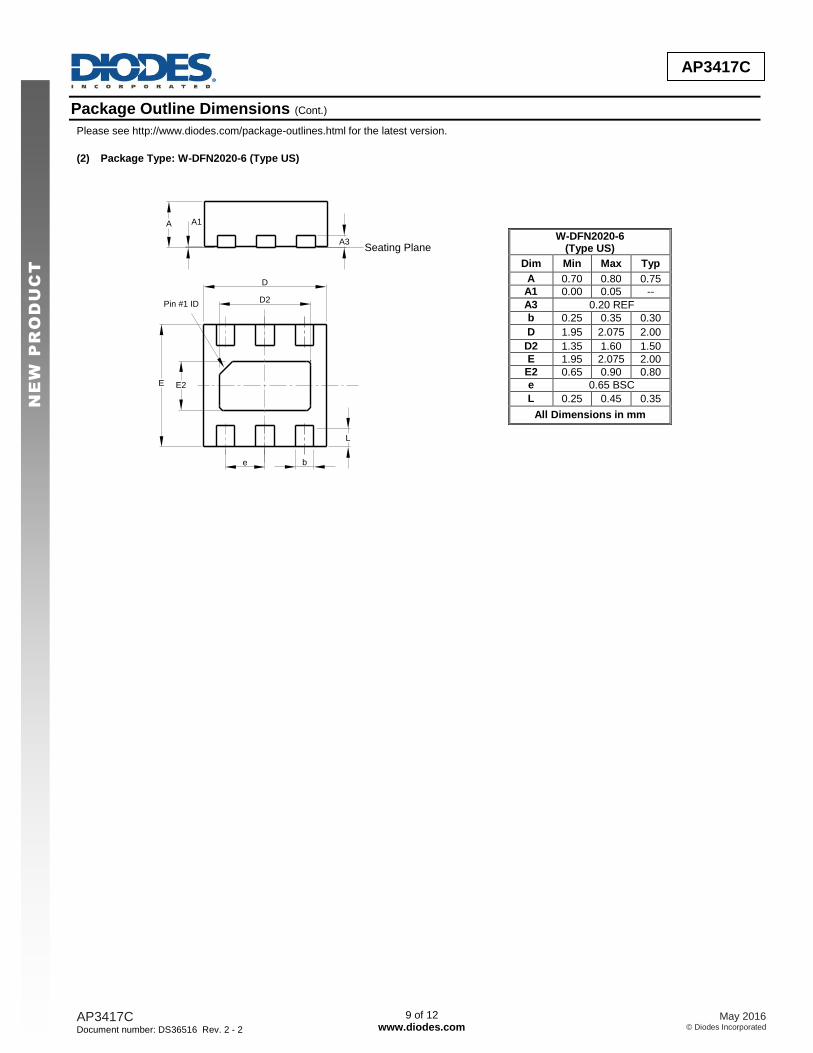
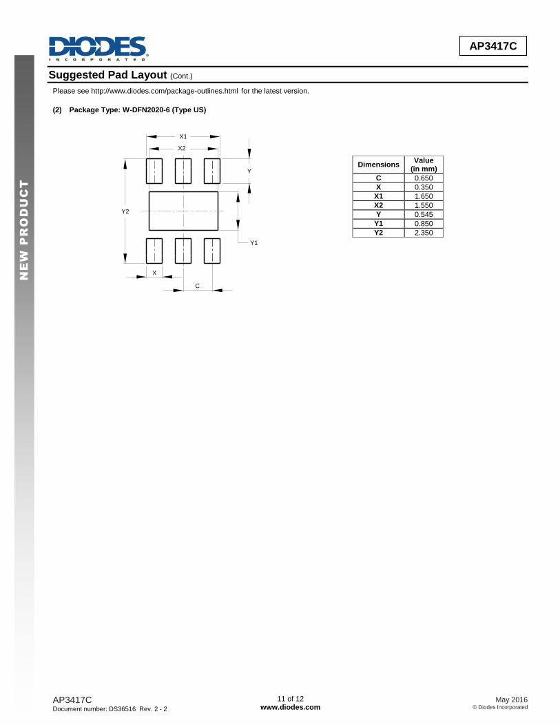
(2) Package Type: W-DFN2020-6 (Type US)
W-DFN2020-6 (Type US)
Dim Min Max Typ
A 0.70 0.80 0.75
A1 0.00 0.05 --
A3 0.20 REF
b 0.25 0.35 0.30
D 1.95 2.075 2.00
D2 1.35 1.60 1.50
E 1.95 2.075 2.00
E2 0.65 0.90 0.80
e 0.65 BSC
L 0.25 0.45 0.35
All Dimensions in mm
D
D2
E
e b
L
E2
A A1
A3Seating Plane
Pin #1 ID

AP3417C Document number: DS36516 Rev. 2 - 2
10 of 12 www.diodes.com
May 2016 © Diodes Incorporated
AP3417C
NE
W P
RO
DU
CT
Suggested Pad Layout
(1) Package Type: SOT-23-5
E2
E1
Y
X
G Z
Dimensions Z
(mm)/(inch) G
(mm)/(inch) X
(mm)/(inch) Y
(mm)/(inch) E1
(mm)/(inch) E2
(mm)/(inch)
Value 3.600/0.142 1.600/0.063 0.700/0.028 1.000/0.039 0.950/0.037 1.900/0.075
AP3417C Document number: DS36516 Rev. 2 - 2
11 of 12 www.diodes.com
May 2016 © Diodes Incorporated
AP3417C
NE
W P
RO
DU
CT
Suggested Pad Layout (Cont.)
Please see http://www.diodes.com/package-outlines.html for the latest version.
(2) Package Type: W-DFN2020-6 (Type US)
Dimensions Value
(in mm)
C 0.650
X 0.350
X1 1.650
X2 1.550
Y 0.545
Y1 0.850
Y2 2.350
Y2
X1
X2
Y1
Y
X
C
AP3417C Document number: DS36516 Rev. 2 - 2
12 of 12 www.diodes.com
May 2016 © Diodes Incorporated
AP3417C
NE
W P
RO
DU
CT
IMPORTANT NOTICE DIODES INCORPORATED MAKES NO WARRANTY OF ANY KIND, EXPRESS OR IMPLIED, WITH REGARDS TO THIS DOCUMENT, INCLUDING, BUT NOT LIMITED TO, THE IMPLIED WARRANTIES OF MERCHANTABILITY AND FITNESS FOR A PARTICULAR PURPOSE (AND THEIR EQUIVALENTS UNDER THE LAWS OF ANY JURISDICTION). Diodes Incorporated and its subsidiaries reserve the right to make modifications, enhancements, improvements, corrections or other changes without further notice to this document and any product described herein. Diodes Incorporated does not assume any liability arising out of the application or use of this document or any product described herein; neither does Diodes Incorporated convey any license under its patent or trademark rights, nor the rights of others. Any Customer or user of this document or products described herein in such applications shall assume all risks of such use and will agree to hold Diodes Incorporated and all the companies whose products are represented on Diodes Incorporated website, harmless against all damages. Diodes Incorporated does not warrant or accept any liability whatsoever in respect of any products purchased through unauthorized sales channel. Should Customers purchase or use Diodes Incorporated products for any unintended or unauthorized application, Customers shall indemnify and hold Diodes Incorporated and its representatives harmless against all claims, damages, expenses, and attorney fees arising out of, directly or indirectly, any claim of personal injury or death associated with such unintended or unauthorized application. Products described herein may be covered by one or more United States, international or foreign patents pending. Product names and markings noted herein may also be covered by one or more United States, international or foreign trademarks. This document is written in English but may be translated into multiple languages for reference. Only the English version of this document is the final and determinative format released by Diodes Incorporated.
LIFE SUPPORT Diodes Incorporated products are specifically not authorized for use as critical components in life support devices or systems without the express written approval of the Chief Executive Officer of Diodes Incorporated. As used herein: A. Life support devices or systems are devices or systems which: 1. are intended to implant into the body, or
2. support or sustain life and whose failure to perform when properly used in accordance with instructions for use provided in the labeling can be reasonably expected to result in significant injury to the user.
B. A critical component is any component in a life support device or system whose failure to perform can be reasonably expected to cause the failure of the life support device or to affect its safety or effectiveness. Customers represent that they have all necessary expertise in the safety and regulatory ramifications of their life support devices or systems, and acknowledge and agree that they are solely responsible for all legal, regulatory and safety-related requirements concerning their products and any use of Diodes Incorporated products in such safety-critical, life support devices or systems, notwithstanding any devices- or systems-related information or support that may be provided by Diodes Incorporated. Further, Customers must fully indemnify Diodes Incorporated and its representatives against any damages arising out of the use of Diodes Incorporated products in such safety-critical, life support devices or systems. Copyright © 2016, Diodes Incorporated www.diodes.com