EMBEDDED TEST CIRCUIT AND METHOD FOR …ufdcimages.uflib.ufl.edu/UF/E0/01/56/57/00001/yoon_j.pdf1.1...
168
EMBEDDED TEST CIRCUIT AND METHOD FOR RADIO FREQUENCY (RF) SYSTEMS-ON-A-CHIP (SOCS) By JANG-SUP YOON A DISSERTATION PRESENTED TO THE GRADUATE SCHOOL OF THE UNIVERSITY OF FLORIDA IN PARTIAL FULFILLMENT OF THE REQUIREMENTS FOR THE DEGREE OF DOCTOR OF PHILOSOPHY UNIVERSITY OF FLORIDA 2006
Transcript of EMBEDDED TEST CIRCUIT AND METHOD FOR …ufdcimages.uflib.ufl.edu/UF/E0/01/56/57/00001/yoon_j.pdf1.1...

EMBEDDED TEST CIRCUIT AND METHOD FOR RADIO FREQUENCY (RF)
SYSTEMS-ON-A-CHIP (SOCS)
By
JANG-SUP YOON
A DISSERTATION PRESENTED TO THE GRADUATE SCHOOL OF THE UNIVERSITY OF FLORIDA IN PARTIAL FULFILLMENT
OF THE REQUIREMENTS FOR THE DEGREE OF DOCTOR OF PHILOSOPHY
UNIVERSITY OF FLORIDA
2006

Copyright 2006
by
JANG-SUP YOON

This document is dedicated to my parents, my son, and my wife.

iv
ACKNOWLEDGMENTS
I would like to express my sincere gratitude to my advisor, Professor William R.
Eisenstadt, for his devoted support and encouragement throughout my work. Without his
invaluable support and encouragement, my exploration in the research could not have
come to fruition. It has been a great pleasure to have been his student. I also would like
to thank Professors Robert M. Fox, Kenneth K. O and Loc Vu-Quoc for their advice on
this work and their willing service on my committee. I appreciate their interest in my
work and their valuable suggestions and comments from the research proposal to its
realization. I would like to especially thank Professor Robert M. Fox for his invaluable
and timely advice and encouragement to continue my work every time I eagerly look for
a breakthrough.
I would like to thank the Semiconductor Research Corporation (SRC) and Na-
tional Science Foundation (NSF) for the sponsorship of this work. I also would like to
thank IBM for the chip fabrication.
I would like to thank my colleagues Hyeopgoo Yoo, Sanghoon Choi, Kooho Jung,
Jongsik Ahn, Ming He, Qizhang Yin, Tao Zhang, Choongeol Cho, Yuseok Ko, Xiaoqing
Zhou, Xueqing Wang, Jiwoon Yang, Dongjun Yang, Inchang Seo, Okjune Jeon, and
Youngki Kim for their helpful discussions, advice, and friendship. Their support and
advice have contributed immensely to my work. Also, I thank all of the friends who made
my years at the University of Florida such an enjoyable chapter of my life

v
Finally, I am grateful to my parents, Hoyoung Yoon and Jungja Kwon, my sister,
Sunghee Yoon, and brother, Wonsup Yoon, for their love and encouragement throughout
the years. I would like to express my profound thanks to my wife, Youngsim Kim, for her
unconditional and never-ending love and support, and my dearest son, Sungroa. Without
them, it would not have been possible to pursue my graduate studies.

vi
TABLE OF CONTENTS Page ACKNOWLEDGMENTS ................................................................................................. iv
LIST OF TABLES........................................................................................................... viii
LIST OF FIGURES .............................................................................................................x
ABSTRACT..................................................................................................................... xvi
CHAPTER 1 INTRODUCTION ........................................................................................................1
1.1 Reason for Embedded RF Test. ..............................................................................1
1.2 Research Goals .......................................................................................................2
1.3 Outline of the Dissertation......................................................................................3
2 LUMPED PASSIVE CIRCUITS FOR EMBEDDED TEST OF RF SoCs .................5
2.1 Introduction.............................................................................................................5
2.2 Design of Lumped Passive Directional Coupler ..................................................10
2.3 Design of Lumped Passive Balun and Divider.....................................................21
2.4 Simulation of Lumped Passive Devices ...............................................................27
2.5 Fabrication Results of Lumped Passive Devices..................................................38
2.6 Conclusion ............................................................................................................43
3 EMBEDDED LOOPBACK FOR RF ICs TEST........................................................46
3.1 Introduction...........................................................................................................46
3.2 Embedded IC Test for WLAN SoCs ....................................................................47
3.3 Design of Loopback Circuit..................................................................................49
3.4 Simulation of Loopback Sub-circuits and System................................................58
3.5 Measured Results of Loopback Sub-circuits and Test System.............................67
3.6 Conclusions...........................................................................................................73

vii
4 ANOTHER EMBEDDED LOOPBACK FOR RF ICs TEST....................................75
4.1 Introduction...........................................................................................................75
4.2 Design of Loopback Circuit Type 2 .....................................................................77
4.3 Simulation of Loopback Sub-circuits and System Type 2 ...................................79
4.4 Measured Results of Loopback Test Type 2 System............................................86
4.5 Conclusions...........................................................................................................88
5 EMBEDDED S-PARAMETER MEASUREMENT Module ....................................89
5.1 Introduction...........................................................................................................89
5.2 Introduction of Scattering Parameters ..................................................................92
5.3 Introduction of Mixed Mode Scattering Parameter ..............................................96
5.4 Design for On-Chip Scattering Parameter Measurement .....................................99
5.5 Simulation for On-Chip Scattering Parameter Measurement. ............................110
5.6 Measured Results................................................................................................115
5.7 S-parameter Application.....................................................................................119
5.8 Conclusions.........................................................................................................122
6 SUMMARY AND CONCLUSION .........................................................................125
6.1 Summary.............................................................................................................125
6.2 Conclusion ..........................................................................................................126
APPENDIX SPIRAL INDUCTOR MODELING USING HFSS........................................................130
A.1 Overview............................................................................................................130
A.2 Definition of Quality Factor ..............................................................................131
A.3 Inductance Calculation Using Y-parameter.......................................................132
A.4 Another Calculation Method for Spiral Inductor...............................................134
A.5 Material Assignment for Spiral Inductor Modeling ..........................................136
A.6 Simulation and Measurement of Spiral Inductor...............................................137
A.7 De-embedding Method for Spiral Inductor .......................................................140
A.8 Another De-embedding Method for Spiral Inductor .........................................143
A.9 Conclusion .........................................................................................................145 LIST OF REFERENCES.................................................................................................146
BIOGRAPHICAL SKETCH ...........................................................................................151

viii
LIST OF TABLES
Table page 2-1 Specification for the commercial directional coupler....................................................6
2-2 Specification for the lumped passive directional coupler..............................................7
2-3 Specification for the commercial divider ......................................................................8
2-4 Specification for the lumped passive divider ................................................................8
2-5 Specification for the commercial balun.........................................................................9
2-6 Specification for the lumped passive balun...................................................................9
2-7 Calculation and simulation value for the directional coupler......................................28
2-8 Calculated value of the equivalent circuit for the directional coupler.........................30
2-9 Calculation and simulation value for divider ..............................................................32
2-10 Calculated value of the equivalent circuit for the divider .........................................34
2-11 Calculation and simulation value for the hybrid .......................................................37
3-1. The resistor values of various attenuators ..................................................................53
3-2. Calculated value of the equivalent circuit for LNA ...................................................64
3-3. Calculated value of the equivalent circuit for embedded loopback............................66
4-1. Calculated value of the equivalent circuit for LNA of Type 2...................................81
4-2. Calculated value of the equivalent circuit for directional coupler of Type 2 .............83
4-3. Calculated value of the equivalent circuit for the embedded loopback Type 2 .........85
5-1. Specification of the commercial network analyzer and on-chip s-parameter module91
5-2. Calculation and simulation value of 10 GHz directional coupler ............................110
5-3. Calculated value of the phase detector circuit (Type I)............................................113

ix
5-4. Calculated value of the HBT Cherry-Hooper amplifier ...........................................113
5-5. Calculated value of the peak detector.......................................................................115
6-1. Design summary .......................................................................................................128

x
LIST OF FIGURES
Figure page 2-1. RF&IF block diagram...................................................................................................5
2-2. Directional coupler and detector...................................................................................7
2-3. The basic concept of directional coupler....................................................................10
2-4. Equivalent capacitance network .................................................................................11
2-5. Even mode and odd mode of transmission line..........................................................12
2-6. Transmission line model.............................................................................................13
2-7. Even mode analysis of coupler and equivalent lumped model ..................................14
2-8. Open case of center symmetric line in even-mode and equivalent circuit .................15
2-9. Short case of center symmetric line in even-mode and equivalent circuit .................16
2-10. Odd mode analysis of coupler and equivalent lumped model..................................17
2-11. Short case of center symmetric line in odd-mode and equivalent circuit.................18
2-12. Open case of center symmetric line in odd-mode and equivalent circuit.................19
2-13. Directional coupler and equivalent lumped model...................................................20
2-14. Symbol for a balun ...................................................................................................21
2-15. Symbol for a divider .................................................................................................21
2-16. Π model ....................................................................................................................22
2-17. T-model ....................................................................................................................25
2-18. Schematic of lumped passive directional coupler ....................................................27
2-19. The layout of the lumped-passive directional coupler..............................................29
2-20. The model of interconnection line............................................................................29

xi
2-21. The equivalent circuit of metal line..........................................................................30
2-22. Simulation results of lumped-passive-directional coupler .......................................31
2-23. Schematic of lumped passive divider .......................................................................32
2-24. The layout of the lumped-passive the divider ..........................................................33
2-25. The model of interconnection line............................................................................34
2-26. Simulation results of a lumped-passive divider........................................................35
2-27. A ring hybrid (rat-race).............................................................................................36
2-28. Schematic of a lumped passive hybrid .....................................................................36
2-29. Simulation results of the lumped-passive balun .......................................................37
2-30. Die micrograph (1.0mm x 1.2mm) of the lumped-passive-directional coupler .......38
2-31. Simulated and measured results of the lumped-passive-directional coupler............39
2-32. Die micrograph (1.0mm x 0.8mm) of the lumped-passive divider ..........................40
2-33. Simulated and measured results of the lumped-passive-divider ..............................40
2-34. Die micrograph (1.0mm x 1.2mm) of the lumped-passive hybrid ...........................41
2-35. Simulated and measured results of the lumped-passive-divider ..............................42
3-1. WLAN block diagram ................................................................................................47
3-2. Block diagram of embedded loopback RFIC test.......................................................48
3-3. The resistor type attenuator ........................................................................................49
3-4. The SPDT (single pole double throw) switches .........................................................54
3-5. N-channel MOSFET model........................................................................................55
3-6. The schematic of RF switch .......................................................................................55
3-7. The parasitic model of n-MOS with control resistance..............................................57
3-8. The simulated results of the RF switch with and without control resistance .............57
3-9. The schematic of the cascode low noise amplifier (LNA) .........................................58
3-10. Simulation result of pi-type attenuator .....................................................................59

xii
3-11. The gate model for optimum insertion loss of RF switch ........................................60
3-12. Simulated results of gate width (finger number) sweep from 60 to 120 at 5.2 GHz61
3-13. Simulated results of gate length sweep from 400 nM to 1300 nM at 5.2 GHz ........62
3-14. Simulated results of the RF switch ...........................................................................62
3-15. The schematic of the cascode low noise amplifier with parasitics...........................63
3-16. Simulated results of the low noise amplifier with parasitics ....................................64
3-17. The block diagram of the embedded loopback test model .......................................65
3-18. The block diagram of the embedded loopback test model with parasitics...............65
3-19. Simulated results of the loopback with parasitics circuit output power level at port 266
3-20. Die micrograph (1.0mm x 1.2mm) of the RF attenuator and RF switch..................67
3-21. Measured results of various pi-type attenuators .......................................................68
3-22. Model of the RF attenuator and substrate.................................................................69
3-23. Layout of the RF attenuator with and without substrate contact ..............................70
3-24. Die micrograph (1.6mm x 1.1mm) of the RF attenuator and RF switch..................71
3-25. Measured results of the 30 dB attenuator .................................................................71
3-26. Measured results of the RF switch ...........................................................................72
3-27. Die micrograph (1.85mm x 0.87mm) of the embedded loopback test model ..........73
3-28. Measured results of the embedded loopback test model ..........................................73
4-1. Block diagram of another embedded loopback RFIC test..........................................75
4-2. The block diagram of embedded loopback test model Type 2...................................77
4-3. The schematic of cascode low noise amplifier (LNA) ...............................................78
4-4. The schematic of 10 dB directional coupler...............................................................79
4-5. Simulated results of the RF switch .............................................................................80
4-6. The schematic of cascode low noise amplifier with parasitics for Type 2.................80
4-7. S-parameter simulation result of the low noise amplifier with parasitics for Type 2 82

xiii
4-8. Gain simulation result of the low noise amplifier with parasitics for Type 2 ............82
4-9. The schematic of lumped passive directional coupler with parasitics for Type 2......83
4-10. S-parameter simulation result of the directional coupler with parasitics for Type 284
4-11. The block diagram of embedded loopback test model Type 2 with parasitics.........85
4-12. Simulated results of the loopback Type 2 with parasitics ........................................86
4-13. Die micrograph (1.6mm x 1.2mm) of the embedded loopback test model ..............87
4-14. Measured results of the embedded loopback test Type 2 model..............................87
5-1. Transmission line and equivalent circuit ....................................................................92
5-2. Function diagram of s-parameter................................................................................95
5-3. Signal diagram of mixed mode two-port network......................................................96
5-4. Conceptual diagram of mixed-mode two-port............................................................98
5-5. Traditional block diagram for s-parameter measurement.........................................100
5-6. Receiver block diagram of traditional s-parameter measurement ............................100
5-7. Conceptual block diagram for on-chip s-parameter measurement...........................101
5-8. The schematic of 10 dB directional coupler for 10 GHz..........................................102
5-9. The schematic of DPST switch for 10 GHz .............................................................103
5-10. Flip-flop phase detector as a phase detector (type I) ..............................................105
5-11. The schematic of phase detector type I ..................................................................106
5-12. Exclusive-OR gate as a phase detector (type II).....................................................106
5-13. The schematic of phase detector type II .................................................................107
5-14. The schematic of Cherry-Hooper amplifier............................................................108
5-15. The concept of strong impedance mismatch ..........................................................109
5-16. The schematic of voltage-divider enhanced RF power detector ............................109
5-17. Simulation results of 10 GHz directional coupler ..................................................110
5-18. Schematic of the 10 GHz RF switch ......................................................................111

xiv
5-19. Simulated results of the 10 GHz RF switch ...........................................................112
5-20. The simulated results of the phase detector type I at 10 GHz ................................112
5-21. The simulation of HBT Cherry-Hooper amplifier..................................................113
5-22. Structure of the type II phase detector....................................................................114
5-23. Simulated results of the phase detector type II at 10 GHz .....................................114
5-24. Simulated results of the peak detector....................................................................115
5-25. Die micrograph (1.0mm x 1.2mm) of the phase detector type I and DPDT switch116
5-26. The measured results of the DPDT switch .............................................................116
5-27. The measured results of the DPDT switch .............................................................117
5-28. Die micrograph (2.2mm x 1.2mm) of the phase detector type II and phase detector118
5-29. The measured results of the phase detector type II with Cherry-Hooper amplifier118
5-30. The measured results of the peak detector..............................................................119
5-31. Block diagram for verification of s-parameter measurement .................................119
5-32. Peak detection of s-parameter measurement module .............................................120
5-33. Phase detection of s-parameter measurement module............................................121
5-34. Example of s-parameter measurement application.................................................122
5-35. Phase error calculation with calibration to 0 dBm reference of s-parameter measurement module..............................................................................................124
A-1. Spiral inductor modeling for 3D-EM simulation.....................................................132
A-2. The equivalent circuit of spiral inductor..................................................................132
A-3. Two port Π-model. ..................................................................................................133
A-4. 2-port network of spiral inductor. ............................................................................134
A-5. Excitation for spiral inductor with GSG pad. ..........................................................138
A-6. Simulation and measurement result of spiral inductor. ...........................................139
A-7. Open and short structure for de-embedding. ...........................................................141
A-8. The simulation and measured results of open and short structure...........................142

xv
A-9. Simulated and measured result of de-embedding spiral inductor............................143
A-10. Another de-embedding structure for spiral inductor. ............................................144
A-11. Simulated and measured result of de-embedding spiral inductor..........................144

xvi
Abstract of Dissertation Presented to the Graduate School of the University of Florida in Partial Fulfillment of the Requirements for the Degree of Doctor of Philosophy
EMBEDDED TEST CIRCUIT AND METHODS FOR RADIO FREQUENCY (RF) SYSTEMS-ON-A-CHIP (SOCS)
By
Jang-Sup Yoon
August 2006
Chair: William Eisenstadt Major Department: Electrical and Computer Engineering
This proposal mainly focuses on research in embedded test circuit and methods for
RF SoCs. First, lumped passive circuits for embedded test of RF SoCs are discussed.
Many companies have been trying to integrate an entire WLAN system on a SoC. Such a
high level integration calls for research in embedded tests for the SoC. The 802-11a
WLAN embedded IC test requires 5 GHz directional couplers, baluns, and dividers,
which are presented in this proposal. Lumped passive 5 GHz ICs were developed to
realize these compact test devices.
Second, an embedded loop back for RF ICs test is described. The loopback test is
one of the lowest cost methods for verifying functionality in a communication circuit.
Thus, the loopback test is employed in mature product lines where cost is an over-riding
concern or as a final test after other circuit tests. On-chip or on-wafer loopback circuits
are designed for verifying performance of 5 GHz wireless WLAN IC circuits.

xvii
Finally, an embedded s-parameter measurement method is discussed. Testing and
verification of the RF and microwave components are major parts of the total testing cost.
This is so because very expensive RF and microwave test equipment (for example, A
vector network analyzer) should be used for this test. Over the years, various methods
have been considered to reduce testing costs. A new method is an on-wafer s-parameter
measurement which is a very economical method for keeping high level accuracy.

1
CHAPTER 1 INTRODUCTION
1.1 Reason for Embedded RF Test.
A recent design trend in RF/analog technologies is to design Systems-on-a-Chip
(SoCs), which include mixed-signal/RF circuit designs. Due to advanced process
technologies, more advanced analog circuits, RF, and microwave circuits can all be
integrated. As chips become more integrated with mixed-signal/RF circuits, more
complex, higher frequency and more accurate test equipment is needed to verify SoC
performance.
In this highly competitive industry, both chip performance and chip costs are
considered important factors for industry success. Testing in this commercial market,
especially mixed-signal/RF circuits, is becoming a major cost factor in overall IC
manufacturing costs, and is the primary main reason that most IC manufacturers have
sought to research and develop new, more economically viable, test methods for mixed-
signal/RF circuits.
Furthermore, newly developed process technologies will make for more complex
chips. For this reason, high performance test equipment is needed to verify SoC
performance in today’s IC production tests. However, mixed-mode ATE systems with 10
GHz test capability add significant test costs to manufactured part costs, and complicated
test procedures require increased testing time. Therefore, traditional ATE tests are no
longer low cost, and chip designers and test engineers want to find more advanced testing
methods for more highly integrated chips.

2
A proposed solution for the high cost of tests is embedded RF test. To verify chip
performance, some of the parameters, for example s-parameters, may be extracted from
the IC for RF testing. A method of RF microwave component on-chip or on-wafer test
has potentially huge technical advantages compared to traditional measurement methods.
One advantage of on-wafer measurements is the elimination of package effects, and
another advantage is that there are fewer complex RF test fixture effects than traditional
measurement methods. Due to these advantages, embedded RF test methods may support
more accurate component characterization. The important test trade off in this on-chip
test research is test accuracy versus required area and power on the IC.
1.2 Research Goals
The first goal of this research is to generate lumped passive circuits for 5 GHz
embedded test of RF SoCs. Many companies have been trying to integrate the whole
WLAN system on a SoC. Such a high level of integration calls for research to embedded
test for the WLAN SoC. A WLAN embedded IC test can require 5 GHz directional
couplers, baluns, and dividers, which are presented in this work. Lumped passive 5 GHz
ICs were developed to realize these compact test devices. Measurement results show
excellent agreement with simulation for the integrated 5 GHz coupler, balun and divider
designs.
The second goal of this research is to realize embedded loop back for RF IC test.
This research explores the use of on-chip or on-wafer loopback for verifying performance
of 5 GHz wireless LAN IC circuits. The loopback measurement is made for a simplified
transceiver circuit. This research is exploratory in nature, and is the first attempt at a new
on-chip RF test technique.

3
Finally, this research develops a new embedded s-parameter measurement method.
At RF microwave frequencies, embedded s-parameter measurements are considered an
essential measurement method. The s-parameters of a DUT (Device-Under-Test) provide
a clear interpretation of the small signal transmission and reflection performance of the
DUT. The detection and measurement of level and phase difference between two signals
are key points of s-parameter measurements.
1.3 Outline of the Dissertation
This dissertation has been organized into six chapters and an appendix. An
overview of this research is given in the current chapter, including the importance of
embedded RF test, the research goals, and the scope of this work. An appendix presents a
spiral inductor modeling method using HFSS. In this appendix, more accurate modeling
methods and faster simulation methods are reviewed.
Chapter 2 presents some lumped passive circuits for embedded test of RF SoCs. In
this chapter, a lumped passive directional coupler, lumped passive divider, lumped
passive balun, and lumped passive hybrid for embedded test and differential
measurement of RF ICs are reviewed.
In chapters 3 and 4, a method for embedded loop back of RF ICs Test is presented.
RF switches, and loopback test circuits have been designed and characterized for
embedded test of RF ICs. Simplified transceiver on-chip loopback circuits were built and
tested, and the performance is shown as well as the design and probing difficulties.
An embedded s-parameter measurement method is introduced in chapter 5. This
chapter discusses basic concepts and shows a block diagram to implement the proposed
idea, and also discusses the weak points and design bottlenecks of the embedded s-
parameter measurement method. To realize the proposed idea, a directional coupler,

4
DPDT (Double-Pole Double-Throw) switch, peak detector, and phase detector are
designed and a possible implementation method is briefly presented.
Chapter 6 summarizes the dissertation and presents future work for after the
dissertation.

5
CHAPTER 2 LUMPED PASSIVE CIRCUITS FOR EMBEDDED TEST OF RF SOCS
2.1 Introduction
Recent design trends in RF/analog technologies show integration Systems-on-a-
Chip (SoCs) and include mixed-signal/RF circuit design. In today’s production tests,
expensive equipment is needed to verify SoC performance. For example, mixed-mode
ATE systems with 3 GHz test capability can add significant test costs to a manufactured
part cost.
BPF
ANT
ANT
SW SW
LNA BPF
MIXER
HPA BPF AMP
MIXER
LO SYNTH
Receiver
Transmitter
DeMOD
MOD
AMP
BPF
ANT
ANT
SW SW
LNA BPF
MIXER
HPA BPF AMP
MIXER
LO SYNTH
Receiver
Transmitter
DeMOD
MOD
AMP
Fig. 2-1. RF&IF block diagram
To realize RF/analog signal test on the SoC, each part (RF and IF block and digital
control block) should be tested simultaneously. As shown in Figure 2-1, the RF and IF
blocks consist of three function units (receiver, transmitter, and synthesizer). Testing the
6
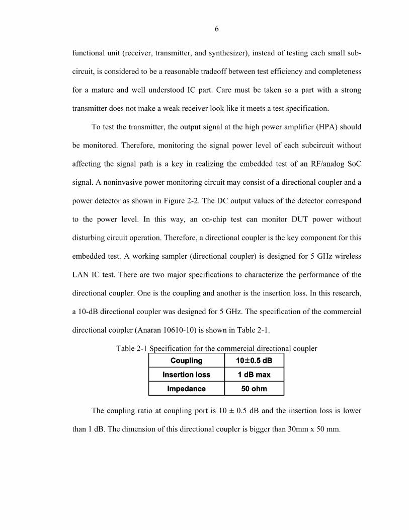
functional unit (receiver, transmitter, and synthesizer), instead of testing each small sub-
circuit, is considered to be a reasonable tradeoff between test efficiency and completeness
for a mature and well understood IC part. Care must be taken so a part with a strong
transmitter does not make a weak receiver look like it meets a test specification.
To test the transmitter, the output signal at the high power amplifier (HPA) should
be monitored. Therefore, monitoring the signal power level of each subcircuit without
affecting the signal path is a key in realizing the embedded test of an RF/analog SoC
signal. A noninvasive power monitoring circuit may consist of a directional coupler and a
power detector as shown in Figure 2-2. The DC output values of the detector correspond
to the power level. In this way, an on-chip test can monitor DUT power without
disturbing circuit operation. Therefore, a directional coupler is the key component for this
embedded test. A working sampler (directional coupler) is designed for 5 GHz wireless
LAN IC test. There are two major specifications to characterize the performance of the
directional coupler. One is the coupling and another is the insertion loss. In this research,
a 10-dB directional coupler was designed for 5 GHz. The specification of the commercial
directional coupler (Anaran 10610-10) is shown in Table 2-1.
Table 2-1 Specification for the commercial directional coupler
50 ohmImpedance
1 dB maxInsertion loss
10±0.5 dBCoupling
50 ohmImpedance
1 dB maxInsertion loss
10±0.5 dBCoupling
The coupling ratio at coupling port is 10 ± 0.5 dB and the insertion loss is lower
than 1 dB. The dimension of this directional coupler is bigger than 30mm x 50 mm.

7
Table 2-2 Specification for the lumped passive directional coupler
50 ohmImpedance
2 dB maxInsertion loss
10±0.5 dBCoupling
50 ohmImpedance
2 dB maxInsertion loss
10±0.5 dBCoupling
The proposed directional coupler is designed using the lumped passive circuits to
realize it on the silicon wafer. So the target area for this directional coupler is less than 1
mm2. Even though dramatically less area is employed compared with a commercial
directional coupler, the proposed specification for the lumped directional coupler has the
same coupling and less than 2 dB insertion loss as shown in the Table 2-2.
Coupler
Detector
Input Through
Isolated Coupled
OutputCoupler
Detector
Input Through
Isolated Coupled
Output
Fig. 2-2. Directional coupler and detector
Other proposed lumped passive circuits are the lumped passive balun and the
lumped passive divider. Most of RF applications adopt single-ended (common-mode)
analyses. But in balanced circuits, common-mode analysis and differential-mode analysis
must be considered [Bok97] [Bok95]. Similar to the directional coupler case, the working
sample is designed for a 5 GHz wireless LAN IC test. There are three major
specifications to characterize the performance of the divider. One is the phase difference

8
between two dividing ports and the second is the insertion loss. The third is the amplitude
difference between two ports. The lumped passive divider was designed for 5 GHz. The
specification of the commercial divider (Meca 802-2-6.000) is shown in Table 2-3. The
phase difference between two ports are 0 ± 4˚ and the insertion loss is low than 1 dB. The
amplitude difference between two ports is within 1.5 dB and the dimension of this divider
is bigger than 25mm x 20 mm.
Table 2-3 Specification for the commercial divider
50 ohmImpedance
1.5 dB maxAmplitude difference
0± 4˚Phase difference
1.0 dB maxInsertion loss
50 ohmImpedance
1.5 dB maxAmplitude difference
0± 4˚Phase difference
1.0 dB maxInsertion loss
The proposed divider is designed using the lumped passive circuits to realize it on
the silicon wafer. Similar to the lumped passive direction coupler, the target area for the
lumped passive divider is less than 1 mm2. The proposed specification for the lumped
passive divider is shown in the Table 2-4.
Table 2-4 Specification for the lumped passive divider
50 ohmImpedance
1.5 dB maxAmplitude difference
0± 4˚Phase difference
1.5 dB maxInsertion loss
50 ohmImpedance
1.5 dB maxAmplitude difference
0± 4˚Phase difference
1.5 dB maxInsertion loss
On the other hand, analyzing the differential-mode [Bok00] requires a device (a
balun) that divides signals into two branches with equal magnitude and opposite polarity
(180° out of phase). This working sample also is designed for 5 GHz wireless LAN IC
test. Similar to the divider, there are three major specifications to characterize the
performance of the balun. One is the phase difference between two dividing ports and the

9
second is the insertion loss. The third is the amplitude difference between two dividing
ports. The lumped passive balun was designed for 5 GHz operation. The specification of
the commercial balun (Johanson Technology 5250BL14B100) is shown in Table 2-5. The
phase difference between two ports are 180 ± 15˚ and the insertion loss is lower than 1
dB. The amplitude difference between the two ports is within 1.5 dB and the dimension
of this divider is roughly 1.6mm x 0.8 mm.
Table 2-5 Specification for the commercial balun
50 ohmImpedance
1.5 dB maxAmplitude difference
180± 15˚Phase difference
1.0 dB maxInsertion loss
50 ohmImpedance
1.5 dB maxAmplitude difference
180± 15˚Phase difference
1.0 dB maxInsertion loss
The proposed balun is designed using the lumped passive circuits to realize it on
the silicon wafer. Similar to the lumped passive directional coupler, the target area for
lumped passive divider is less than 1 mm2. The proposed specification for the lumped
passive balun is shown in Table 2-6.
Table 2-6 Specification for the lumped passive balun
50 ohmImpedance
1.5 dB maxAmplitude difference
180± 15˚Phase difference
1.5 dB maxInsertion loss
50 ohmImpedance
1.5 dB maxAmplitude difference
180± 15˚Phase difference
1.5 dB maxInsertion loss
As mentioned already, for embedded IC test, a directional coupler, a balun and
divider are needed. The traditional method to realize these passive circuits uses
microstrip lines or lumped passive components [Par89]. Unfortunately, the quarter-wave
length at 5 GHz is almost 8 mm and is too big for on-chip realization. Therefore making
the lumped-passive circuits is the only practical option.

10
2.2 Design of Lumped Passive Directional Coupler
The lumped passive circuit design style is as follows. First, a distributed microstrip
circuit is designed with a large area, and then a compact lumped equivalent circuit is
extracted from the distributed circuit. Second, the design of the coupled line directional
coupler for 5 GHz is presented. The main function of this directional coupler is to sample
power from sources. Directional couplers[Bah03] are also used for measuring unknown
impedances, detecting antenna faults, and combining and or splitting power. There are
various types of directional couplers including branch line couplers, wave guide couplers,
Lange couplers [Lan69], Wilkinson dividers [Wil60] and coupled line directional
couplers [Mon55].
The coupled line directional coupler [Poz97][Mal88][Mal79] is one of the most
popular directional couplers at microwave frequency bands. When the transmission lines
are located close to each other, power will be coupled as shown in Figure 2-3. The
coupler consists of a pair of transmission lines and is modeled as a 4-port network. Most
of the launched power at port 1 will be delivered to port 4. Due to the interaction of the
electromagnetic fields, some power will be coupled to port 2. As shown in Figure 2-2, if
port 1 and port 4 are considered the input port and output port, respectively, port 2
becomes the coupling port and port 3 becomes an isolation port.
Port 1
Input
Port 2
C oupling
Port 4
Transm it
Port 3
Isolation
Port 1
Input
Port 2
C oupling
Port 4
Transm it
Port 3
Isolation
Fig. 2-3. The basic concept of directional coupler

11
Typically the coupled transmission lines operate in TEM mode, and the electrical
characteristics of the coupled lines can be modeled as a function of the effective
capacitances between the lines. As shown in Figure 2-4, the coupled transmission lines
parameters C11, C22, and C12. C12 are defined as the capacitance between the two
transmission lines, while, C11 and C22 are defined as the capacitance between the
transmission lines and the ground. If the widths of the two transmission lines and the
distance of the transmission lines from ground are the same, then C11 will equal C22.
1 2
C12C11 C22
1 2
C12C11 C22
Fig.2-4. Equivalent capacitance network
In analyzing the coupled line directional coupler, one should consider the even and
odd modes. As shown in Figure 2-5-(a), in the even mode, the current flows in the same
direction with the same magnitude, and the electric flux is symmetric with respect to the
H-wall. Conversely, in the odd mode, as shown in Figure 2-5-(b), the current flows in the
opposite direction with the same magnitude, and the electric flux is also symmetric with
respect to the E-wall. In this case, conductor 1 is emitting electric flux while conductor 2
is sinking flux thus making the E-wall an equipotential surface with V=0, and the E-wall
acting as the ground plane.

12
1 2
H-wall
+V +V
1 2
H-wall
+V +V
(a) Even-mode
1 2
E-wall
+V -V
1 2
E-wall
+V -V
(b) Odd-mode
Fig. 2-5. Even mode and odd mode of transmission line
As shown Figure 2-5, the coupled line directional coupler consists of two
transmission lines. For analysis, each transmission line can be modeled as shown in
Figure 2-6. The voltage at the source (x=-l) and the load (x=0) can be equated as follows:
ljLs eVV β−= (2.1)
( ) ( )ljO
ljs eeVlVV ββ −+ Γ+=−= (2.2)
( ) ( )OL VVV Γ+== + 10 , where OL
OLO ZZ
ZZ+−
=Γ (2.3)

13
The input impedance of the transmission line with the characteristic impedance of
Z0, and the termination load of ZL, can be expressed as,
(2.4)
Also the voltage at the source can be expressed as the function of the voltage of the
load (VL), the load impedance (ZL), the characteristic impedance (ZO), and the electrical
length lβ .
(2.5)
ZL
ZO
ZIN
VS VL
X=0X= -l
+
-
+
-
ZL
ZO
ZIN
VS VL
X=0X= -l
+
-
+
-
Fig. 2-6. Transmission line model
If V1=VS, V4=VL, βl=θ, Z1=1/y1=ZO/ZL, then
θθθθ sincossincos1
1
1
11
4
jyy
jZVV
+=
+= (2.6)
The coupling factor is
(2.7)
(2.8)
OOOe
OOOe
ZZZZ
+−
=C
CCZOOe −
+=
11Z
ljZZljZZ
L
L
ββ
tantanZZ
0
00in +
+=
( )lZZjl L ββ sincosVV 0LS +=

14
(2.9)
To design a 10 dB coupled directional coupler, one calculates Zoe and Zoo. To
realize the coupled line directional coupler, the line width (W) value and the line spacing
(S) between two lines should be calculated first. This complex manipulation is beyond
the dissertation focus. To convert a coupled-line-directional coupler to a lumped-passive-
directional-coupler [Par89] [Son02], first the even-mode is handled.
θ
Yin
Yoe
θ
Yin
Yoe
(a) Coupled-line coupler
Ce Ce
2 Le
YinCe Ce
2 Le
Yin
(b) Equivalent lumped model
Fig. 2-7. Even mode analysis of coupler and equivalent lumped model
The directional coupler has horizontal symmetry (with respect to the two parallel
lines) due to the H-field wall and vertical symmetry (symmetry axis with respect to the
center of transmission lines) due to its symmetrical structure. Therefore, the analysis for
half of one transmission line can be used for the whole directional coupler as shown in
CCZOOO +
−=
11Z

15
Figure 2-7. If the center symmetric line is open as shown in Figure 2-8, the input
impedance of the coupler is
ein sC
Z 12
cot jZ 0e =−=θ (2.10)
2 tan jZ 0o
θ=esC (2.11)
2 tan
Z 0o θω
=eC (2.12)
θ/2
Zin
Zoe
θ/2
Zin
Zoe
(a) Even-mode open case
Ce
Le
ZinCe
Le
Zin
(b) Equivalent Circuit
Fig. 2-8. Open case of center symmetric line in even-mode and equivalent circuit
16
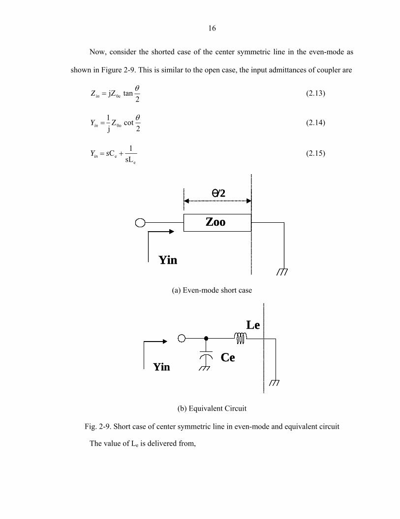
Now, consider the shorted case of the center symmetric line in the even-mode as
shown in Figure 2-9. This is similar to the open case, the input admittances of coupler are
2 tan jZ 0e
θ=inZ (2.13)
2cot Z
j1 0o
θ=inY (2.14)
ee sL
1 C += sYin (2.15)
θ/2
Yin
Zoo
θ/2
Yin
Zoo
(a) Even-mode short case
Ce
Le
YinCe
Le
Yin
(b) Equivalent Circuit
Fig. 2-9. Short case of center symmetric line in even-mode and equivalent circuit
The value of Le is delivered from,

17
ee0o sL
1 C 2
cotjZ +=− sθ (2.16)
θω
sin 2Z oe=eL (2.17)
The next step is solving for the odd-mode case. The odd-mode, with the E-wall
located horizontally, acts as a ground plane at the center as shown in Figure 2-10.
θ
Zin
Zoo
θ
Zin
Zoo
(a) Coupled-line coupler
Zin
Ce CeLe Le
2Co
Lo LoZin
Ce CeLe Le
2Co
Lo Lo
(b) Equivalent lumped model
Fig. 2-10. Odd mode analysis of coupler and equivalent lumped model
For a vertically symmetric shorted line, the equivalent circuit is shown in Figure 2-
11.

18
Θ/ 2
Yin
Yoo
Θ/ 2
Yin
Yoo
(a) Odd-mode short case
YinLeCe Lo
YinLeCe Lo
(b) Equivalent Circuit
Fig. 2-11. Short case of center symmetric line in odd-mode and equivalent circuit
The input impedance of transmission line as shown in Figure 2-11-(a) becomes
(2.18)
(2.19)
And the input admittance of the equivalent circuit in Figure 2-11-(b) is
(2.20)
The even-mode equivalent parameters are derived (Ce, Le, Zoo and Zoe); Lo is
formed by using a simple manipulation.
⎟⎠⎞
⎜⎝⎛ −+
=
θθθω
sin12
2tan
2cot
1 oooooe
o
ZZZL (2.21)
Since θ=90°, Lo simplifies as
2cot θ
ooin jYY −=
2 tan jZ 0
θ=inZ
oe Lj1
Lj1
ωωω ++= ein CjY

19
( )oooeo ZZ
L−
=ω
1 (2.22)
Given that the vertical symmetric line is open, the equivalent circuit as shown in
Figure 2-12-(b).
Θ/ 2
Yin
YooOpen
Θ/ 2
Yin
YooOpen
(a) Odd-mode short case
Yin
Le
Ce Lo CoYin
Le
Ce Lo Co
(b) Equivalent Circuit
Fig. 2-12. Open case of center symmetric line in odd-mode and equivalent circuit
The input impedance of transmission line in Figure 2-12-(a) becomes
(2.23)
(2.24)
And the input admittance of the equivalent circuit in Figure 2-12-(b) is
(2.25)
2 tan θ
ooin jYY =
2cot jZ 0
θ−=inZ
oe
ein
CjL
CjY
ωωω
ω 1j
1 Lj
1 o +++=

20
The even-mode and odd-mode equivalent parameters (Ce, Le, Lo, Zoo and Zoe) are
already found. Co is formed by using a simple manipulation.
( )( )( )oooeoe
oooeo ZZZ
ZZC−+
−=
1sin2 θω
(2.26)
Since θ=90°, simplified Co is
( )( )( )oooeoe
oooeo ZZZ
ZZC−+
−=
12 ω
(2.27)
Finally, the equivalent lumped model of a directional coupler with every element is
shown in Figure 2-13.
θ
Zoe, Zoo
Symmetric planeθ
Zoe, Zoo
Symmetric plane
(a) Coupled-line coupler
Port 1 Port 3
Port 2 Port 4
CeCe
Ce Ce
Le Le
Le Le2Lo Co 2Lo
Port 1 Port 3
Port 2 Port 4
CeCe
Ce Ce
Le Le
Le Le2Lo Co 2Lo
(b) Equivalent lumped model
Fig. 2-13. Directional coupler and equivalent lumped model

21
2.3 Design of Lumped Passive Balun and Divider
Two other important on-chip test circuits are the balun and the divider. The balun is
a three-port network with a 180° phase difference between the two output ports. With
reference to the balun shown in Figure 2-14, a signal launched into port 1 will be evenly
split into two components with a 180° phase difference at port 2 and port 3.
Fig. 2-14. Symbol for a balun
The divider, is also a three-port network, but with the same phase between the two
output ports. As shown in Figure 2-15, a signal launched into port 1 will be evenly split
into two in-phase components forwards 2 and port 3.
12
3
90°
90°
12
3
90°
90°
Fig. 2-15. Symbol for a divider
The balun is created by combining a 90° phase delay branch and a 270° phase delay
branch. The divider is created by combining two 90° phase delay branches. The
12
3
90°
270°
12
3
90°
270°

22
scattering matrix of a 90° phase delay branch is labeled as [S1] and the scattering matrix
of a 270° phase delay branch is labeled as [S2].
⎟⎟⎠
⎞⎜⎜⎝
⎛=⎟⎟
⎠
⎞⎜⎜⎝
⎛∠
∠=
0 j-j- 0
0 901901 0
S1 (2.28)
⎟⎟⎠
⎞⎜⎜⎝
⎛=⎟⎟
⎠
⎞⎜⎜⎝
⎛∠
∠=
0 jj 0
0 27012701 0
S2 (2.29)
This phase delay branch of the scattering matrix [S1] can be modeled as a Π model
as shown in Figure 2-16. All series and shunt components are given as admittances Y1,
Y2 and Y3.
Y3
Y 2Y 1
Y 3
Y 2Y 1
Fig. 2-16. Π model
The ABCD parameters for Figure 2-16 are;
(2.30)
(2.31)
(2.32)
3
1Y
B =
3
21YYA +=
3
2121 Y
YYYYC ++=

23
(2.33)
If Y1=Y2, then the ABCD parameters reduce into;
(2.34)
(2.35)
(2.36)
(2.37)
Using a table of conversions for two-port network parameters, the s-parameters of
this Π model are obtained.
(2.38)
(2.39)
(2.40)
(2.41)
DCZZBA
DCZZBA
S+++
−−+=
00
00
11( )
( ) 121212
0300312
02
1
2031
20
21
++++−+−
=ZYZZYYZY
ZYYZY
DCZZBA
DCZZBA
S+++
+−+−=
00
00
22( )
( ) 121212
0300312
02
1
2031
20
21
++++−+−
=ZYZZYYZY
ZYYZY
( )DCZZ
BABCADS
+++−
=0
0
122
( ) 12122
0300312
02
1
03
++++=
ZYZZYYZYZY
DCZZBA
S+++
=0
0
212
( ) 12122
0300312
02
1
03
++++=
ZYZZYYZYZY
3
21
12YYYC +=
3
11YYA +=
3
11YYD +=
3
1Y
B =
3
11YYD +=

24
(2.42)
Since S11 = S22 = 0,
(2.43)
(2.44)
(2.45)
(2.46)
Substituting Y3 to equation “S12 = -j”,
(2.47)
01 Z
jY = (2.48)
01
1Z
Cω
= (2.49)
( )0
201
20
21
3 21
Zj
ZYZY
Y −=
−= (2.50)
ω0
3ZL = (2.51)
The other phase delay branch of the scattering matrix [S2] can be modeled as a T
model as shown in Figure 2-17. All series and shunt components are given as impedances
Z1, Z2 and Z3.
( ) 12122
0300312
02
1
0312 ++++=
ZYZZYYZYZYS ( ) j
ZYZY
−=+−−
=11
01
01
( )201
20
21
3 21
ZYZYY −
=
( ) 12 312
01 =+ YYZY
12 2031
20
21 =+ ZYYZY
( )( )
01212
12
0300312
02
1
2031
20
21
11 =++++
−+−=
ZYZZYYZYZYYZYS
⎥⎦
⎤⎢⎣
⎡=
0 j-j- 0
S
( )( ) ( )
( )( )
( ) ⎥⎥⎥⎥⎥
⎦
⎤
⎢⎢⎢⎢⎢
⎣
⎡
++++−+−
++++
++++++++−+−
=
1212
12 1212
2
1212
2 1212
12
0300312
02
1
2031
20
21
0300312
02
1
03
0300312
02
1
03
0300312
02
1
2031
20
21
ZYZZYYZYZYYZY
ZYZZYYZYZY
ZYZZYYZYZY
ZYZZYYZYZYYZY

25
Z 1 Z 2
Z 3
Z 1 Z 2
Z 3
Fig. 2-17. T-model
The ABCD parameters for Figure 2-17 are;
(2.52)
(2.53)
(2.54)
(2.55)
If Z1=Z2, then the ABCD parameters reduce into,
(2.56)
(2.57)
(2.58) 3
1Z
C =
3
11ZZA +=
3
1Z
C =
3
11ZZA +=
3
2121 Z
ZZZZB ++=
3
21ZZD +=
3
21
12ZZZB +=

26
(2.59)
Using table of Conversions for Two-Port Network Parameters, the S-parameters of
this T model are obtained.
(2.60)
(2.61)
(2.62)
(2.63)
(2.64)
Since S11 = S22 = 0,
(2.65)
(2.66)
(2.67)
Substituting Z3 to equation “S12 = j”,
( ) 02 3112
0 =+− ZZZZ
1
21
20
3 2ZZZZ −
=
( )( )( ) ( )
022
2
3113102
0
3112
011 =
+++++−−
=ZZZZZZZ
ZZZZS
3
11ZZD +=
DCZZBA
DCZZBA
S+++
−−+=
00
00
11( )( )
( ) ( )3113102
0
3112
0
222
ZZZZZZZZZZZ
+++++−−
=
DCZZBA
DCZZBA
S+++
+−+−=
00
00
22( )( )
( ) ( )3113102
0
3112
0
222
ZZZZZZZZZZZ
+++++−−
=
( ) ( )3113102
0
30
222
ZZZZZZZZZ
++++=
( )DCZZ
BABCADS
+++−
=0
0
122
DCZZBA
S+++
=0
0
212
( ) ( )3113102
0
30
222
ZZZZZZZZZ
++++=
⎥⎦
⎤⎢⎣
⎡=
0 jj 0
S
( )( )( ) ( ) ( ) ( )
( ) ( )( )( )
( ) ( ) ⎥⎥⎥⎥⎥
⎦
⎤
⎢⎢⎢⎢⎢
⎣
⎡
+++++−−
++++
+++++++++−−
=
3113102
0
3112
0
3113102
0
30
3113102
0
30
3113102
0
3112
0
222
222
22
2 22
2
ZZZZZZZZZZZ
ZZZZZZZZZ
ZZZZZZZZZ
ZZZZZZZZZZZ
27
(2.68)
jZZ −=1 (2.69)
01
1Z
Cω
= (2.70)
01
21
20
3 2jZ
ZZZ
Z =−
= (2.71)
ω0
3Z
L = (2.72)
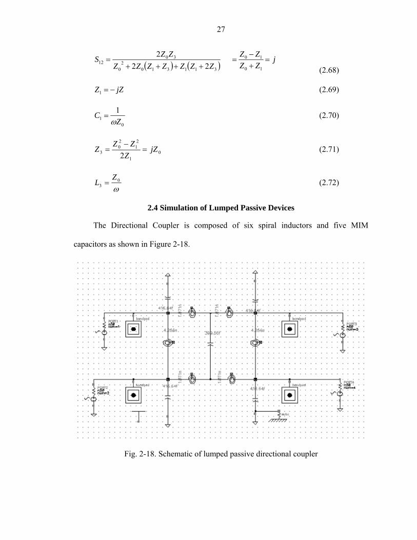
2.4 Simulation of Lumped Passive Devices
The Directional Coupler is composed of six spiral inductors and five MIM
capacitors as shown in Figure 2-18.
Fig. 2-18. Schematic of lumped passive directional coupler
( ) ( )3113102
0
3012 22
2ZZZZZZZ
ZZS++++
= jZZZZ
=+−
=10
10
28
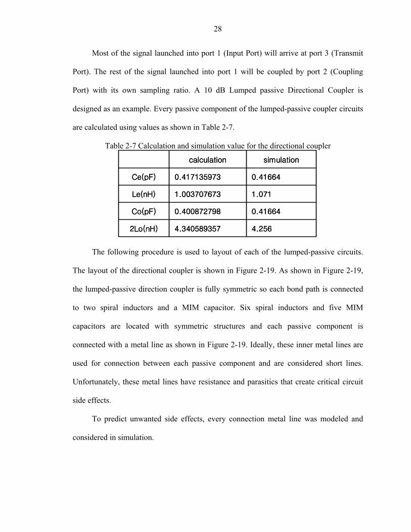
Most of the signal launched into port 1 (Input Port) will arrive at port 3 (Transmit
Port). The rest of the signal launched into port 1 will be coupled by port 2 (Coupling
Port) with its own sampling ratio. A 10 dB Lumped passive Directional Coupler is
designed as an example. Every passive component of the lumped-passive coupler circuits
are calculated using values as shown in Table 2-7.
Table 2-7 Calculation and simulation value for the directional coupler
4.2564.3405893572Lo(nH)
0.416640.400872798Co(pF)
1.0711.003707673Le(nH)
0.416640.417135973Ce(pF)
simulationcalculation
4.2564.3405893572Lo(nH)
0.416640.400872798Co(pF)
1.0711.003707673Le(nH)
0.416640.417135973Ce(pF)
simulationcalculation
The following procedure is used to layout of each of the lumped-passive circuits.
The layout of the directional coupler is shown in Figure 2-19. As shown in Figure 2-19,
the lumped-passive direction coupler is fully symmetric so each bond path is connected
to two spiral inductors and a MIM capacitor. Six spiral inductors and five MIM
capacitors are located with symmetric structures and each passive component is
connected with a metal line as shown in Figure 2-19. Ideally, these inner metal lines are
used for connection between each passive component and are considered short lines.
Unfortunately, these metal lines have resistance and parasitics that create critical circuit
side effects.
To predict unwanted side effects, every connection metal line was modeled and
considered in simulation.
29
Fig. 2-19. The layout of the lumped-passive directional coupler
① ②
③
④
⑥
⑤
① ②
③
④
⑥
⑤
Fig. 2-20. The model of interconnection line
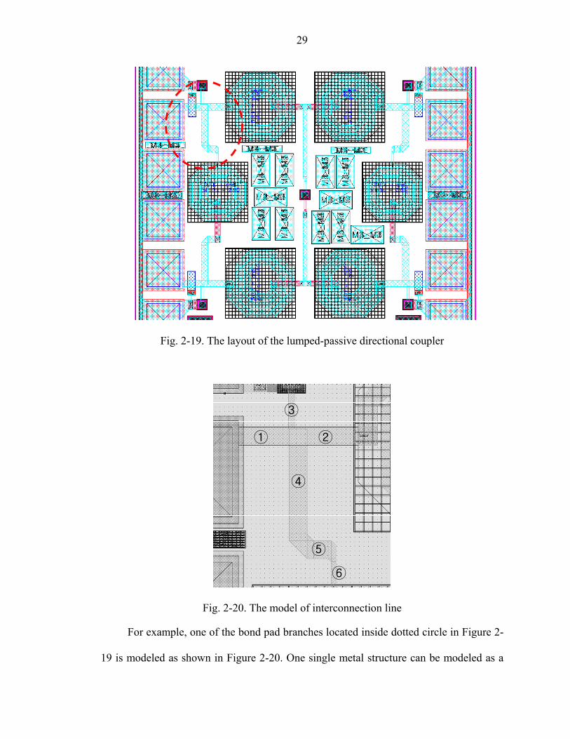
For example, one of the bond pad branches located inside dotted circle in Figure 2-
19 is modeled as shown in Figure 2-20. One single metal structure can be modeled as a

30
combination of six metal segments. A single metal line on silicon wafers can be modeled
as shown in Figure 2-21 [Nik00]. Each metal line has a series inductance L and series
resistance rx and parasitic capacitance C1 and C2 that exist between the metal structure
and substrate. Also, there exists substrate resistances R1 and R2.
L rx
C1
R1
C2
R2
L rx
C1
R1
C2
R2
Fig. 2-21. The equivalent circuit of metal line
All the parasitics in the single metal structure shown in Figure 2-20 are calculated
by the EM simulator ASITIC which is developed by Berkeley and each value is shown in
Table 2-8
Table 2-8 Calculated value of the equivalent circuit for the directional coupler
4.055k4.261f4.055k4.261f48.74m33.03p②20X74.1
4.438k1.737f4.438k1.737f62.24m21.43p③6.62X43.5
3.791k5.91f3.791k5.91f78.07m61.31p④116.22X20
69.92m
24.65m
38.03m
Rx
1.703f
2.695f
3.592f
C1
4.44k1.703f4.44k20.54p⑥40.28X5
4.375k2.695f4.375k13.31p⑤20X39.38
4.184k3.592f4.184k23.76p①20X58.7
R2C2R1L
4.055k4.261f4.055k4.261f48.74m33.03p②20X74.1
4.438k1.737f4.438k1.737f62.24m21.43p③6.62X43.5
3.791k5.91f3.791k5.91f78.07m61.31p④116.22X20
69.92m
24.65m
38.03m
Rx
1.703f
2.695f
3.592f
C1
4.44k1.703f4.44k20.54p⑥40.28X5
4.375k2.695f4.375k13.31p⑤20X39.38
4.184k3.592f4.184k23.76p①20X58.7
R2C2R1L
Finally, a 10 dB lumped-passive-directional coupler was designed with all the side
effects of the connecting metal lines. Two simulation results are shown in Figure 2-22.

31
The original simulation result does not consider parasitics of metal connection lines and
the complete simulation result includes all parasitics of metal line connections. As shown
in Figure 2-22, at 5 GHz the original simulation result for the signal magnitude at port3 is
approximately -0.9 dB, and about 80 % of the power will be delivered to port3 (transmit
port). Also, at 5 GHz the original simulation result for the magnitude at port2 is
approximately -12 dB, and about 6 % of the power will be coupled to port2 (coupling
port). The complete simulation results for the magnitude at port3 and port2 are -1.7 dB
and -9.0 dB respectively. The insertion loss (S31) is increased and coupling (S21) is
decreased due to inter-connection loss and parasitics. These unwanted parasitics change
the frequency response of the lumped passive directional coupler.
-30
-25
-20
-15
-10
-5
0
1 2 3 4 5 6 7 8Frequency
dB
Sim_original s21(dB)Sim_original s31(dB)Sim_complete s21(dB)Sim_complete s31(dB)
Fig. 2-22. Simulation results of lumped-passive-directional coupler
A divider has two 90° phase shift branches as shown in Figure 2-23-(a). The signal
launched into the input port will arrive at the output ports with the same magnitude and
phase. A divider is composed of two spiral inductors, four MIM capacitors and one poly-
resistor as shown in Figure 2-23-(b).

32
3
1
2
√2 Z0 90°
√2 Z0 90°
Z0
Z 0
Z 0
3
1
2
√2 Z0 90°
√2 Z0 90°
Z0
Z 0
Z 0
(a)
(b)
Fig. 2-23. Schematic of lumped passive divider
The passive components of lumped-passive circuits are calculated using introduced
equation as shown in Table 2-9.
Table 2-9 Calculation and simulation value for divider
100100R(ohm)
0.45750.4502C(pF)
2.272.2507L(nH)
simulationcalculation
100100R(ohm)
0.45750.4502C(pF)
2.272.2507L(nH)
simulationcalculation

33
The layout of the following directional coupler is shown in Figure 2-24. Passive
components are used for circuit function. Two spiral inductors, a poly resister and four
MIM capacitors are located with symmetric structures and each passive component is
connected with metal lines as shown in Figure 2-24. These metal lines have resistances
and parasitics. These unwanted resistances and parasitics give rise to critical circuit side
effects.
Fig. 2-24. The layout of the lumped-passive the divider
To predict unwanted side effects, connecting metal lines are modeled for a
complete simulation. For example, one of the bond pad branches located inside the dotted
circle in Figure 2-24 is modeled as shown in Figure 2-25. One single metal structure can
be modeled as a combination of these six metal segments. Each metal line has a series
inductance L and series resistance rx. And parasitic capacitance C1 and C2 can model each
metal structure and substrate. Also, there exists substrate resistance in R1 and R2.

34
Therefore the single metal line on this silicon wafer can be modeled as shown in Figure
2-21 [Nik00].
① ② ③
④⑤
⑥
① ② ③
④⑤
⑥
Fig. 2-25. The model of interconnection line
All parasitics in the single metal structure as shown in Figure 2-25 are calculated
by EM simulator ASITIC developed by Berkeley and each value is shown in Table 2-10
Table 2-10 Calculated value of the equivalent circuit for the divider
4.517k1.934f4.517k1.934f21.66m9.112p②28.38X15
4.037k5.674f4.037k5.674f362.6m62.6p③101.48X15
4.054k4.742f4.054k4.742f10.64m8.571p④55.13X39.48
45.25m
22.62m
28.37m
Rx
7.773f
787.1a
6.509f
C1
3.699k7.773f3.699k49.98p⑥117.32X39.84
4.754k787.1a4.754k3.788p⑤12.02X4.28
3.852k6.509f3.852k28.54p①81.02X43.08
R2C2R1L
Two simulation results are shown in Figure 2-26. The original simulation result
does not consider any metal line parasitics and the complete simulation result includes all
the metal line parasitics. As shown in Figure 2-26, at 5 GHz the original simulation result
for the magnitude at the output ports is approximately -3.8 dB. The phase balance

35
between output ports is almost 0° throughout the frequency band of 1 to 10 GHz. Further,
up to 5 GHz, the complete simulation result for the magnitude at the output ports is
approximately the same as the original simulation result. At high frequency, frequency
response is altered due in part to parasitic effects especially parasitic capacitances
between the metal structure and the substrate. The phase balance between output ports is
not changed significantly and stays almost 0° throughout the frequency band of 1 to 10
GHz.
-16
-14
-12
-10
-8
-6
-4
-2
1 2 3 4 5 6 7 8 9 10frequency(GHz)
(dB
) Sim_original S31(dB)Sim_original S32(dB)Sim_complete S31(dB)Sim_complete S32(dB)
(a)
-250
-200
-150
-100
-50
0
1 2 3 4 5 6 7 8 9 10frquency(GHz)
(deg
)
Sim_original S31(deg)Sim_original S32(deg)
Sim_complete S31(deg)Sim_complete S32(deg)
(b)
Fig. 2-26. Simulation results of a lumped-passive divider
36
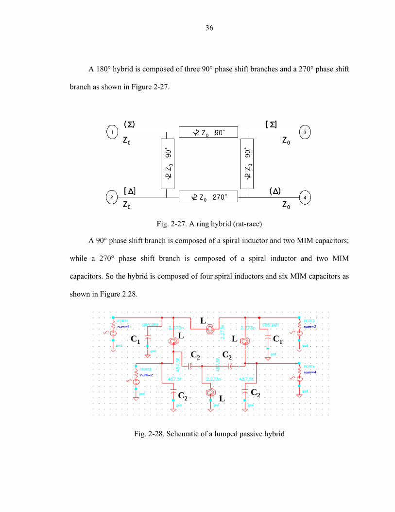
A 180° hybrid is composed of three 90° phase shift branches and a 270° phase shift
branch as shown in Figure 2-27.
1 3
42
(Σ)
(Δ)
√2 Z0 90°
√2 Z
0 90°
√2 Z
0 90°
√2 Z 0 270°
Z0 Z0
Z 0 Z 0
[Σ]
[Δ]
1 3
42
(Σ)
(Δ)
√2 Z0 90°
√2 Z
0 90°
√2 Z
0 90°
√2 Z 0 270°
Z0 Z0
Z 0 Z 0
[Σ]
[Δ]
Fig. 2-27. A ring hybrid (rat-race)
A 90° phase shift branch is composed of a spiral inductor and two MIM capacitors;
while a 270° phase shift branch is composed of a spiral inductor and two MIM
capacitors. So the hybrid is composed of four spiral inductors and six MIM capacitors as
shown in Figure 2.28.
C1 C1
C2 C2
C2C2L
L
LLC1 C1
C2 C2
C2C2L
L
LL
Fig. 2-28. Schematic of a lumped passive hybrid

37
A hybrid is designed utilizing lumped passive components is calculated using
values Table 2-11.
Table 2-11 Calculation and simulation value for the hybrid
0.45750.4502C2(pF)
0.9050.904C1(pF)
2.272.2507L(nH)
simulationcalculation
0.45750.4502C2(pF)
0.9050.904C1(pF)
2.272.2507L(nH)
simulationcalculation
As shown Figure 2-29, at 5.1 ± 0.7 GHz, the original simulation and complete
simulation results show that the magnitude simulation in output ports is approximately
equal to -4.3 dB. The phase balance between these output ports is almost 180° at 5.1 ±
0.7 GHz in the original simulation. At high frequency, especially above 6 GHz, transfer
characteristics are degraded due to parallel parasitic capacitance between metal structures
and the substrate.
-25
-20
-15
-10
-5
0
1 2 3 4 5 6 7 8 9 10
Frequency(GHz)
(dB
)
Sim_original S12(dB)Sim_original S42(dB)Sim_complete S12(dB)Sim_complete S42(dB)
(a)
Fig. 2-29. Simulation results of the lumped-passive balun
38
-450
-400
-350
-300
-250
-200
-150
-100
-50
0
1 2 3 4 5 6 7 8 9 10frequency(GHz)
(deg
)
Sim_original S31(deg)Sim_original S32(deg)Sim_complete S31(deg)Sim_complete S32(deg)
(b)
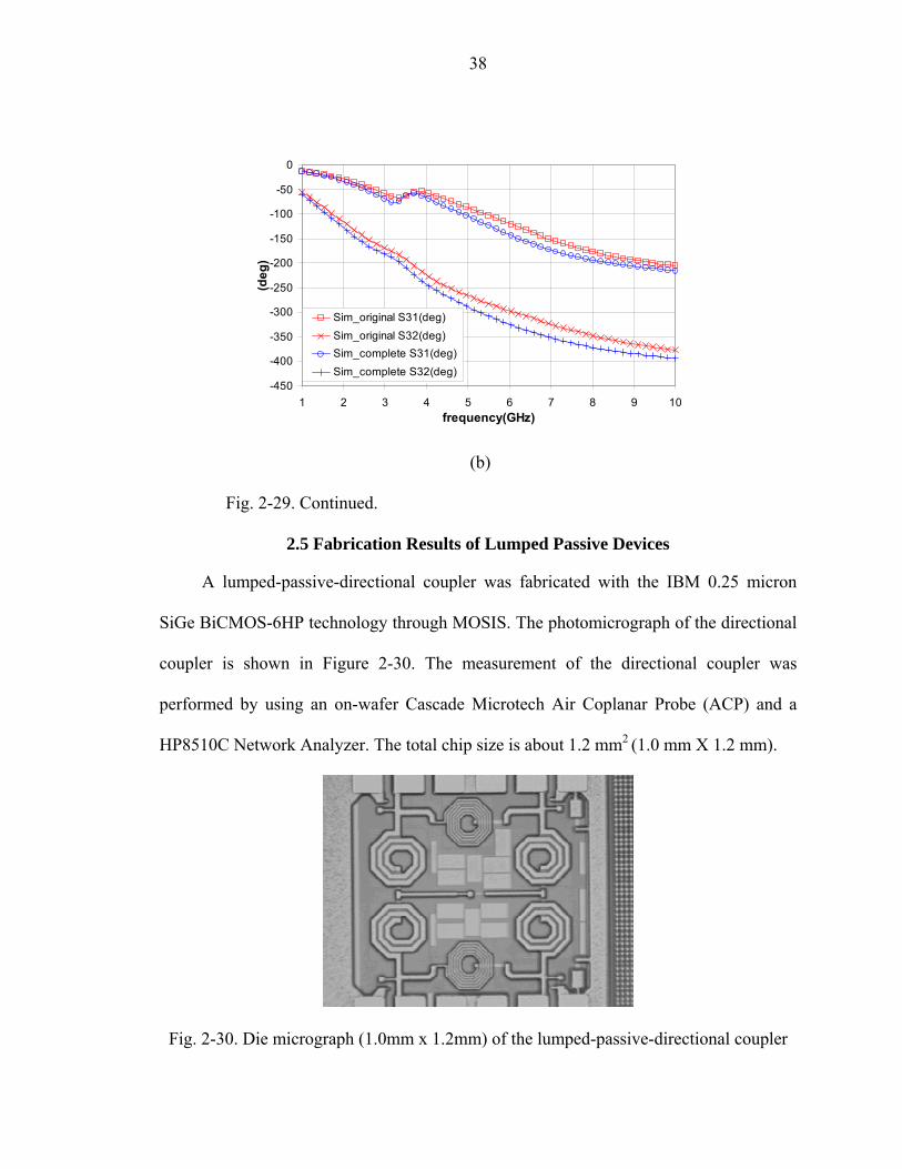
Fig. 2-29. Continued.
2.5 Fabrication Results of Lumped Passive Devices
A lumped-passive-directional coupler was fabricated with the IBM 0.25 micron
SiGe BiCMOS-6HP technology through MOSIS. The photomicrograph of the directional
coupler is shown in Figure 2-30. The measurement of the directional coupler was
performed by using an on-wafer Cascade Microtech Air Coplanar Probe (ACP) and a
HP8510C Network Analyzer. The total chip size is about 1.2 mm2 (1.0 mm X 1.2 mm).
Fig. 2-30. Die micrograph (1.0mm x 1.2mm) of the lumped-passive-directional coupler

39
The measured results of the directional coupler are shown in Figure 2-31. The
transmitted power at transmit port is -2.2 dB at 5.0 GHz including coupling loss of -1.1
dB. The coupling power at the coupling port is -9.5 dB. As mentioned before in Figure 2-
31, the simulated transmit power at the transmit port is -1.7 dB at 5.0 GHz and the
simulated coupling power at the coupling port is -9.0 dB. Compared to the previous
simulation, the measurement results show good agreement.
-30
-25
-20
-15
-10
-5
0
1 2 3 4 5 6 7 8Frequency(GHz)
dB
Measurement s31(dB)Measurement s21(dB)Simulation s21(dB)Simulation s31(dB)
Fig. 2-31. Simulated and measured results of the lumped-passive-directional coupler
The photomicrograph of the divider is shown in Figure 2-32. A lumped-passive-
divider was fabricated with the IBM 0.25 micron SiGe BiCMOS-6HP technology
through MOSIS. The measurement of the directional coupler was performed by using an
on-wafer Cascade Microtech Air Coplanar Probe (ACP) and a HP8510C Network
Analyzer. The total chip size is about 0.8 mm2 (1.0 mm x 0.8 mm).

40
Fig. 2-32. Die micrograph (1.0mm x 0.8mm) of the lumped-passive divider
The measured results of the divider are shown in Figure 2-33. The insertion loss is -
4.07 dB at 5 GHz including a signal splitter loss of 3 dB. The ripple is within ±0.3 dB up
to 6 GHz. The phase difference between the 2 output ports is within 0.5° throughout the
frequency band of 1 to 10 GHz. The simulated insertion loss is -3.8 dB at 5 GHz and the
phase difference between 2 output ports is 0°. The measurement results show good
agreement with the complete simulations.
-16-14-12-10
-8-6-4-2
1 2 3 4 5 6 7 8 9 10frequency(GHz)
(dB
)
Measurement S31(dB)Measurement S32(dB)Simulation S31(dB)Simulation S32(dB)
(a)
Fig. 2-33. Simulated and measured results of the lumped-passive-divider
41
-250
-200
-150
-100
-50
0
1 2 3 4 5 6 7 8 9 10frquency(GHz)
(deg
)
Measurement S31(deg)Measurement S32(deg)Simulation S31(deg)Simulation S32(deg)
(b)
Fig. 2-33. Continued.
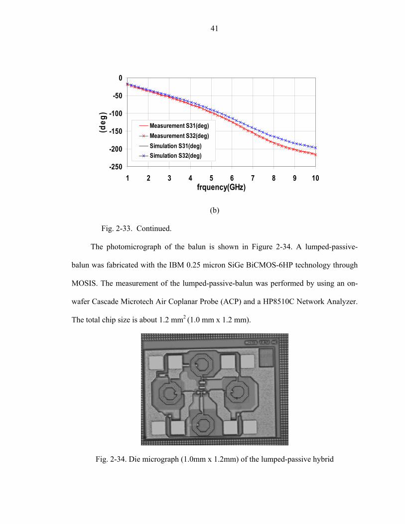
The photomicrograph of the balun is shown in Figure 2-34. A lumped-passive-
balun was fabricated with the IBM 0.25 micron SiGe BiCMOS-6HP technology through
MOSIS. The measurement of the lumped-passive-balun was performed by using an on-
wafer Cascade Microtech Air Coplanar Probe (ACP) and a HP8510C Network Analyzer.
The total chip size is about 1.2 mm2 (1.0 mm x 1.2 mm).
Fig. 2-34. Die micrograph (1.0mm x 1.2mm) of the lumped-passive hybrid

42
The measured results of the balun are shown in Figure 2-35. At 5 GHz, the
insertion losses of the output ports, port1 and port4, are -4.41 dB and -4.47 dB
respectively, including the 3 dB signal splitter loss. The magnitude difference between
the 2 output ports is only 0.06 dB at 5 GHz. The phase balance between two output ports
is approximately 183°~186° at 5.1 ± 0.7 GHz. The simulated insertion losses at 5 GHz
are -3.81 dB at output port1 and -4.17 dB at output port4, and the phase difference
between 2 output ports is 180°~183° at 5.1 ± 0.7 GHz. Therefore, the measurement
shows good agreement with the simulation.
-25
-20
-15
-10
-5
0
1 2 3 4 5 6 7 8 9 10Frequency(GHz)
(dB
)
Measurement S12(dB)Measurement S42(dB)Simulation S12(dB)Simulation S42(dB)
(a)
-450-400-350-300-250-200-150-100
-500
1 2 3 4 5 6 7 8 9 10frequency(GHz)
(deg
)
Measurement S31(deg)Measurement S32(deg)Simulation S31(deg)Simulation S32(deg)
(b)
Fig. 2-35. Simulated and measured results of the lumped-passive-divider

43
2.6 Conclusion
A lumped-passive directional coupler, lumped-passive divider, and hybrid for
embedded test and differential measurement of RF ICs have been designed and tested. As
mentioned already, the traditional method to realize these passive circuits uses microstrip
line. Unfortunately, the quarter-wave length of microstrip at 5 GHz is almost 8 mm and is
too big for on-chip realization. Therefore making the lumped-passive circuits is the only
practical option to implement couplers, dividers and baluns on the silicon wafer.
1) The chip size of a lumped-passive directional coupler is 1 mm2 but only 0.45
mm2 core circuit area is required while the commercial directional coupler needs 1500
mm2. To author’s knowledge, this is the first attempt to design a miniature on-chip
directional coupler design at 5 GHz. To provide more simulation accuracy, the parasitics
of metal lines for interconnection are modeled and considered for simulation. The
transmitted power at transmit port is -2.2 dB at 5.0 GHz including coupling loss of 1.1
dB. Therefore the insertion loss of the lumped passive directional coupler is 1.1 dB. As
shown in Table 2-2, the proposed insertion loss is lower than 2 dB. Another major
specification is the coupling. The designed coupling ratio is 10 dB at 5 GHz and the
proposed specification is 10 ± 0.5 dB at 5 GHz. The measured coupling power at the
coupling port is -9.5 dB. Therefore the designed lumped passive directional coupler
meets the proposed design specification.
2) Similar to the directional coupler, the chip size of a lumped-passive balun is 1
mm2 but only 0.4 mm2 core circuit area is required. Also this is the first attempt to design
a miniaturized on-chip balun design at 5 GHz. To keep more accuracy in simulation, the
parasitics of metal lines for interconnection are modeled and considered in simulation as
44
in the directional coupler design. At 5 GHz, the measured insertion losses of the output
ports, port1 and port4, are 4.41 dB and 4.47 dB respectively, including the 3 dB divider
loss. Therefore, the maximum measured insertion loss is 1.47 dB when the proposed
insertion loss specification maximum is 1.5 dB. The magnitude difference between the 2
output ports is only 0.06 dB at 5 GHz while the specification amplitude difference is
lower than 1.5 dB. The phase balance between the two output ports is approximately
183°~186° at 5.1 ± 0.7 GHz while the specification phase difference is 180 ± 15°.
Therefore the integrated lumped passive balun meets all of the proposed design
specifications.
3) Similar to the directional coupler, the chip size of a lumped-passive balun is 0.8
mm2 but only 0.25 mm2 core circuit area is required. Also, this is the first attempt to
design a miniaturized on-chip divider design at 5 GHz. To keep more accuracy in
simulation, the parasitics of metal lines for interconnection are modeled and considered
for simulation similar to the directional coupler design. At 5 GHz, the measured insertion
losses of the output ports are -4.07 dB including the 3 dB dividing loss. Therefore, the
maximum measured insertion loss is 1.07 dB while the specified maximum insertion loss
is 1.5 dB. The magnitude difference between the 2 output ports is lower than 0.02 dB at 5
GHz while the specified amplitude difference is lower than 1.5 dB. The phase balance
between two output ports is approximately 0° up to 10 GHz while the specified phase
difference is 0 ± 4°. Therefore the designed lumped passive balun also meets all of the
proposed design specifications.
Through this research, the lumped passive directional coupler, divider and balun
were designed for embedded RF IC test on-chip or on-wafer and these integrated lumped

45
passive circuits meet all proposed specification. These lumped passive elements proved
useful in a variety of on-chip RF/microwave test systems including embedded loopback
and on-chip s-parameter test system in future chapters.

46
CHAPTER 3 EMBEDDED LOOPBACK FOR RF ICS TEST
3.1 Introduction
Loopback test is one of the lowest cost test methods for verifying functionality in a
communication circuit. This “go” or “no go” test gives little insight into circuit failure
mechanisms and is of little assistance in debugging a circuit manufacturing process.
Thus, the loopback test is employed in mature product lines where cost is an over-riding
concern [Heu99] [Lup03] or as a final test after other circuit tests. This work assesses the
feasibility of on-chip loopback test for GHz wireless communication ICs. Industry uses
off-chip loopback where transmit signals are routed through a package I/O to a test board
circuit and then back to the receiver of the IC under test. New, on-chip or on-wafer
loopback circuits are designed for verifying performance of 5 GHz wireless WLAN IC
circuits in this research. Although loopback testing is common in mature network
electronics, it has not been applied to on-chip RF systems because 1) there are potential
signal path mismatches, crosstalk and signal leakage problems that adversely affect the
RF/microwave circuit, 2) large amounts of area are consumed, and 3) new on-chip RF
elements are required for implementation. In this dissertation, the author reports on the
test block diagram, the test circuit design and shows test data for loopback test; the key
loopback sub-circuits are microwave attenuators and switches. Simplified transceiver on-
chip loopback circuits have been built and tested. In this dissertation, the performance
and the design are presented. This research is exploratory in nature and is a first attempt
at a new on-chip RF test technique.

47
3.2 Embedded IC Test for WLAN SoCs
Most wireless communications circuits (including WLAN) consist of three basic
blocks (antenna, RF and IF block, and digital processing/control blocks) which are shown
in Figure 3-1. In this figure, the RF and IF block contains a receiver, transmitter, local
synthesizer, switch and band pass filter.
RF & IF BLOCK
Receiver
Transmitter
Switch & B.P.F
LO SYNTH
DIGITAL CONTROL BLOCK
Demodulator
Modulator Encoder
MAC &PHYController
LLC &HigherLayerControl
RF & IF BLOCK
Receiver
Transmitter
Switch & B.P.F
LO SYNTH
DIGITAL CONTROL BLOCK
Demodulator
Modulator Encoder
MAC &PHYController
LLC &HigherLayerControl
Fig. 3-1. WLAN block diagram
The receiver module communicates to the digital processing/control block through
a demodulator and the transmitter module receives its input signal from a modulator
connected to the digital block. Current industry practices may utilize separate production
tests for the transmitter and receiver RF and IF blocks and the digital processing/control
block as well as a complete system test. This process can be costly. On-chip loopback
methods potentially raise the test efficiency and lower test cost of the wireless LAN SoC
in a mature design. Low cost tests will be critical for future low cost consumer parts.
Figure 3-2 shows a WLAN block diagram of the loopback test in which the
transmitter signals test the receiver by connecting them to the receiver through RF
switches with an attenuator in the signal path. In many commercial implementations, the

48
High Power Amplifiers (HPA) are built using different technology (GaAs) and are
separate from the silicon IC transceiver block.
SYNTH
RX BLOCK
RF S/W
S/W
ANT 1
ANT 2
HPA
LNA
BPF AMP
AMP
AGCAMP
AMP AMPBPF
TX BLOCK
MIXER
MIXER
ATT Test Circuit for Embedded testing
CouplerRF S/W
SYNTH
RX BLOCK
RF S/W
S/W
ANT 1
ANT 2
HPA
LNA
BPF AMP
AMP
AGCAMP
AMP AMPBPF
TX BLOCK
MIXER
MIXER
ATT Test Circuit for Embedded testing
CouplerRF S/W
Fig. 3-2. Block diagram of embedded loopback RFIC test
The HPA connects to the antenna (ANT) through the bandpass filter (BPF). In this
loopback test example, test signals are amplified via a preamplifier (AMP) and switched
to either to the HPA input port or to the loopback attenuator and then the LNA via RF
switches. The LNA requires a weak input signal to verify its performance which is
created by the attenuator in the loopback signal path. For example, the minimum
sensitivity of the wireless LAN is -65 dBm. If the amplifier output as shown in Figure 3-2
is -30 dBm, the input signal at LNA is -64 dBm. This signal is the low enough in strength
to characterize the receiver block: the loopback signal path is shown in the shaded region
of Figure 3-2. In summary, Figure 3-2 shows the necessary circuits for demonstrating the
transceiver RF embedded loopback test signal path; these consist of an AMP
(preamplifier), a RF switch, an attenuator, a second RF switch, and a LNA.

49
3.3 Design of Loopback Circuit
The key test circuits for implementing embedded loopback test are high-frequency
attenuators which reduce the transmitted signal to sufficiently low test signal values and
RF switches which are used to modify the signal path between test operation and normal
operation. There are various types of RF switches in communication circuits as like
CMOS switches [Hua01], GaAs switches [Gas78], MEMS switches [Pod00], PIN-diode
switches [Cav92], and Ferrite switches [Cru89]. Also, there are various types of
attenuators such MOS active attenuators [Loh91], PIN-diode attenuators [Bae88],
ferromagnetic attenuators [Tra98], thick film attenuators [Yaz91], and coaxial line
attenuators [Cri79]. The resistor-based attenuator [Poz97][Viz95] was selected as the
most suitable for this embedded loopback RFIC test because it has a wideband circuit
operation and compact implementation. Two kinds of resistor-based attenuators are
considered 1) π-type and 2) T-type. Both attenuators are built from three on-chip resistors
in two port networks as shown in Figure 3-3.
R1 R1
R2
Zo Zo+
-
V1
+
-
V2R1 R1
R2
Zo Zo+
-
V1
+
-
V2
(a) Pi-attenuator
R1
R2
Zo Zo+
-
V1
+
-
V2
R1R1
R2
Zo Zo+
-
V1
+
-
V2
R1
(b) T-attenuator
Fig. 3-3. The resistor type attenuator

50
The π-type attenuator symmetric resistors R1 are the same value as shown in Figure
3-3-(a). If Zo is the port impedance and α is defined as the attenuation value dB, K is
defined as follows (3.1)(3.2).
2010α
=K (3.1)
o
o
ZRZRR
VVK
////
1
12
2
1 +== (3.2)
As shown in Figure 3-3-(a), input impedance of the π-type attenuator is matched at
the port impedance Zo.
)////( 121 oo ZRRRZ += (3.3)
From equation 3.2
( )oo ZRKZRR //// 112 =+ (3.4)
If “ oZRR //12 + ” is “ ( )oZRK //1 ”, then oZ is
( ) ( )⎟⎟⎠
⎞⎜⎜⎝
⎛+
==o
ooo ZR
ZKRRZRKRZ
1
1111 ////// (3.5)
With simple manipulation, oZ is
oo
oo ZKRZRR
ZKRZ
112
1
21
++= (3.6)
From equation 3.6, R1 is
( )( )1
11 −
+=
KKZ
R o (3.7)
K is the attenuation as shown in equation 3.1, thus rewrite (3.7) as

51
⎟⎟⎠
⎞⎜⎜⎝
⎛−
⎟⎟⎠
⎞⎜⎜⎝
⎛+
=
110
110
10
10
1 α
α
oZR (3.8)
A parallel impedance of R1 and Zo is
o
oo ZR
ZRZR
+=
1
11 // (3.9)
R1 is defined as equation (3.7), thus the equation 3.9 is
( )( )( )( )
( )( )
( )( )
( )K
KZ
KK
KKZ
ZKKZ
ZKKZ
ZR oo
oo
oo
o 21
111
11
1111
//1+
=+
−+
−+
=+
−+−+
= (3.10)
From equation (3.4) and equation (3.10), R2 is
( )( ) ( ) ( )K
KZKZRKR o
o 21
1//1 12+
−=−= (3.11)
( )K
KZR o
212
2−
= (3.12)
Finally, R2 is
20102 10)110(
2
αα−
×−= oZR (3.13)
The T-type attenuator symmetric resistors R1 are also the same value as shown in
Figure 3-3-(b). If Zo is the port impedance and α is defined as the attenuation value dB, K
is defined as same way as the π-type attenuator.
( )( )
( )o
o
o
o
ZZR
ZRRZRRR
VV
K+
⋅+++
== 1
12
121
2
1
//// (3.14)
As shown in Figure 3-3-(b), input impedance of the T-type attenuator is matched at
the port impedance Zo.

52
)//( 121 oo ZRRRZ ++= (3.15)
Rewrite the equation (3.15) as
)//( 121 oo ZRRRZ +=− (3.16)
From the equation (3.14) and (3.16), K is
( )( ) ( )
( )1
11
1 RZZR
ZZR
RZZ
Ko
o
o
o
o
o
−+
=+
⋅−
= (3.17)
Thus, R1 is
( )( )1
11 +
−=
KKZ
R o (3.18)
K is the attenuation as shown in equation 3.1, thus rewrite (3.18) as
⎟⎟⎠
⎞⎜⎜⎝
⎛+
⎟⎟⎠
⎞⎜⎜⎝
⎛−
=
110
110
10
10
1 α
α
oZR (3.19)
From the equation (3.16)
o
oo ZRR
RRZRRZ
+++
=−12
1221 (3.20)
Rearrange the equation (3.20) as
( )1212 2 RRRZo += (3.21)
From the equation (3.18) and (3.21)
( )( )
( )( )⎟⎟⎠
⎞⎜⎜⎝
⎛+−
++−
=112
11
22
KKZR
KKZZ ooo (3.22)
( ) oZK
KR1
222 −
= (3.23)
Finally, R2 is

53
110
102
10
20
2
−= α
α
oZR (3.24)
For up to 30 dB attenuation, both π-type and T-type can be realized on-chip but the
T-type attenuator fails at greater than 40 dB attenuation. Table 3-1 shows R2 values of the
T-type attenuator should be ≤ 1 Ω or less for high attenuation values.
Table 3-1. The resistor values of various attenuators
49.990.0150.01250k80
49.970.0350.0379k70
49.900.1050.1025k60
49.680.3250.327.9k50
49.011.0051.012.5k40
46.933.1753.27789.7830
40.9110.1061.11247.5020
25.9735.1496.2571.1510
R1R2R1R2Attenuation(dB)
T-typePi-type
49.990.0150.01250k80
49.970.0350.0379k70
49.900.1050.1025k60
49.680.3250.327.9k50
49.011.0051.012.5k40
46.933.1753.27789.7830
40.9110.1061.11247.5020
25.9735.1496.2571.1510
R1R2R1R2Attenuation(dB)
T-typePi-type
These small resistors are difficult to integrate and easily altered by parasitic
resistances. The π-type topology is employed in 40 dB, 50 dB, and 60 dB on-chip
attenuator designs. The attenuators are built with the IBM BiCMOS technology P+
polysilicon resistors, (good high frequency response) with the same length and width,
(minimize manufacturing variations). R1 is located symmetrically in the layout along the
axis of R2.
The second key component for the embedded loopback RFIC test is the RF switch:
two SPDT (single-pole double-throw) switches are employed. As shown in Figure 3-4-
(a), the port1 is the input port, while port2 and port3 are the output ports. Figure 3-4-(b)

54
shows that a SPDT (single-pole double-throw) switch can be realized by using two on-off
switches.
Port 1Port 2
Port 3Port 1
Port 2
Port 3
(a)
Port 1Port 2
Port 3Port 1
Port 2
Port 3
(b) Fig. 3-4. The SPDT (single pole double throw) switches
In good RF design, most of the launched power at switch port 1 will be delivered to
one of the two output ports and a negligible amount is delivered to the other output port.
In this paper, BiCMOS RF switches are constructed from MOSFETs because they prove
useful in monolithic CMOS and BiCMOS SoC solutions, see Figure 3-5. The insertion
loss, the most important specification of the RF switch design, is controlled by the on-
resistance of the MOSFET. For this reason most RF switches, including these, employ
only n-channel MOSFETs. As shown in Figure 3-5-(c), the parasitic capacitance between
source and drain of the MOSFET is a dominant factor in determining the isolation of the
MOSFET. To realize the optimum RF switch, an equivalent circuit is constructed and the
optimum value of each equivalent component is found. To maintain a high frequency
response, optimum length MOSFETs are used [Hua01].

55
R
Source Drain
GateR
Source Drain
Gate
(a)
R
On-StateSource Drain
R
On-State
RR
On-StateSource Drain
(b)
C
Off-StateSource Drain
C
Off-State
CC
Off-StateSource Drain
(c)
Fig. 3-5. N-channel MOSFET model
Typical CMOS RF switches, according to the literature, are built from four n-
channel MOSFET and four resistors as shown in Figure 3-6-a) [Hua01].
Port 2
Cont_Port2 Cont_Port3
Port 3
Port 1
M1
M2
M3
M4
R1 R3
R2R4
Port 2
Cont_Port2 Cont_Port3
Port 3
Port 1
M1
M2
M3
M4
R1 R3
R2R4
(a)
Fig. 3-6. The schematic of RF switch

56
Port 2
Cont_Port2 Cont_Port3
Port 3
Port 1
M1 M3
R1 R3
Port 2
Cont_Port2 Cont_Port3
Port 3
Port 1
M1 M3
R1 R3
(b)
Fig 3-6. Continued.
In these typical switches, the two MOSFETs perform the switching functions and
the additional two MOSFETs increase the isolation. Isolation performance and test circuit
area are traded off. In this application, this test circuit area is more important then its
isolation performance because isolation can be compensated by other methods. For this
reason, the RF switch is composed of two n-channel MOSFETs and two poly resistors as
shown in Figure 3-6-b) in a compact area design.
The parasitic model of M3 in Figure 3-6 is modeled as shown in Figure 3-7. To
connect port1 to port2, Con_port2 is biased with high voltage and Con_port3 is biased
with low voltage to disconnect port1 to port3. During this time, there is some power
leakage through the parasitic capacitor Cgs3 of M3 as shown in Figure 3-7. Even though
small amounts of power leaks through the parasitic capacitor Cgs3 of M3, the insertion
loss may be decreased dramatically according to this leakage ratio because the gate of M3
is at low impedance ground. So all leakage signal flows into the low impedance. The
other parasitics are not playing a critical role compared to Cgs3. Maintaining the high
impedance at a gate of M3 is one good method to prevent leakage.

57
M3
R3
Cgs3
Cont_Port3Substrate
Csb3 Cdb3Cgd3
Cgb3
M3
R3
Cgs3
Cont_Port3Substrate
Csb3 Cdb3Cgd3
Cgb3
Fig. 3-7. The parasitic model of n-MOS with control resistance
A high resistance value (20 kΩ) is used to control resistor R3. By doing this, the
gate impedance is changed from low impedance to high impedance and the effect of the
parasitic capacitor is significantly decreased. This in turn decreases the RF switch
insertion loss by approximately 0.3 dB as shown in Figure 3-8. The CMOS gate length is
the dominant RF switch insertion loss factor so the minimum length (250 nm device gate
length, 400 nm drawn layout gate lengths) is used.
-4.00
-3.50
-3.00
-2.50
-2.00
-1.50
-1.00
-0.50
0.00
1.0 2.0 3.0 4.0 5.0 6.0 7.0 8.0 9.0 10.0
Frequency(GHz)
Inse
rtio
n lo
ss (d
B)
R=20kR=0
Fig. 3-8. The simulated results of the RF switch with and without control resistance

58
As shown in Figure 3-2, the RF switch and RF attenuator are key components for
the loopback test. To realize this test, additional two amplifiers are needed. One is a low
noise amplifier (LNA) and the other is an amplifier (AMP) as shown in Figure 3-2. A
cascode low noise amplifier was designed as the low noise amplifier[Raz98]. The
schematic diagram is shown in Figure 3-9. The transistor size is designed for optimum
gain and noise figure. For input matching, two spiral inductors are used. One is 2.08 nH
and another is 402 pH as shown in Figure 3-9. Similarly, for output matching, one spiral
inductor and one MIM capacitor are used as shown in Figure 3-9.
Bias Network
Vdd
3.78 nH
121 fF
6x
8x
6.6 pF
402 pH
2.08 nH
5.0 pF
2 k
2 k
Output Matching
Input Matching
Bias Network
Vdd
3.78 nH
121 fF
6x
8x
6.6 pF
402 pH
2.08 nH
5.0 pF
2 k
2 k
Output Matching
Input Matching
Fig. 3-9. The schematic of the cascode low noise amplifier (LNA)
3.4 Simulation of Loopback Sub-circuits and System
Cadence SpectreS was used to design 5 GHz 30 dB, 40 dB, 50 dB, and 60 dB
lumped passive π-type attenuators. As shown in Figure 3-10, at 5 GHz the simulation

59
results for the magnitude at port 2 for the 30 dB attenuator is approximately -30.1 dB.
Similarly, the 40 dB attenuator has a -40.3 dB loss at 5 GHz, the 50 dB attenuator has a -
50.1 dB loss at 5 GHz and the 60 dB attenuator has a -62.1 dB loss. This simulation
includes parasitic parameters (capacitances) of the P+ Polysilicon resisters which degrade
high frequency response.
Fig. 3-10. Simulation result of pi-type attenuator
In these typical switches, the two MOSFETs perform the switching functions and
the additional two MOSFETs increase the isolation. As shown in Figure 3-5-b), the
resistance on on-state is the dominant RF switch insertion loss factor. The gate
impedance can be modeled as shown in Figure 3-11.

60
Length
Width
Length
Width
Fig. 3-11. The gate model for optimum insertion loss of RF switch
The gate width can be modeled as a parallel resistor and parasitic capacitor as
shown in Figure 3-11. As the width increases, the resistance becomes lower and the
insertion loss of the RF switch decreases. But simultaneously, the parasitic capacitor
increases. The parasitic capacitors make the insertion loss of the RF switch worse. The
simulation results which sweep the number of fingers in the MOSFET from 60 to 120
with a gate width of 900 nM is shown in Figure 3-12. When the number of finger is
increased, the insertion loss becomes improves up to 84 fingers. If there are more than 84
fingers, the insertion loss becomes worse. So, the 84 fingers are selected for the minimum
insertion loss RF switch. In reality, it is difficult to layout an n-MOSFET with 84 fingers.
For this layout, 84 metal lines are needed for every gate connection. This also causes
unwanted parasitic capacitance. For practical realization of the MOSFET, the finger
number is reduced from 84 to 8 and each gate width is increased from 900 nM to 9400
nM. By doing this, the total gate width can be kept the same.

61
-4.45
-4.4
-4.35
-4.3
-4.25
-4.2
-4.15
60 80 100 120
Finger number
dB
Fig. 3-12. Simulated results of gate width (finger number) sweep from 60 to 120 at 5.2 GHz
Similarly, the gate length can be modeled as the series resistance as shown in
Figure 3-11. If the gate length is increased, the resistance is increased also. The
simulation results which sweep the gate length from 400 nM to 1300 nM is shown in
Figure 3-13. If the gate length is decreased, the insertion loss of the RF switch is also
decreased. Finally, the insertion loss becomes minimal when the gate length becomes 400
nM. The simulation results show up to a 400 nM gate length because IBM-6HP 0.25
technology can provide 400 nM as a minimum gate length. For this reason, a minimum
length (250 nm device gate length, 400 nm drawn layout gate length) is used for the RF
switch.
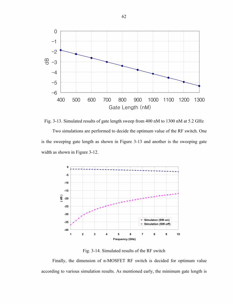
62
-6
-5
-4
-3
-2
-1
0
400 500 600 700 800 900 1000 1100 1200 1300
Gate Length (nM)
dB
Fig. 3-13. Simulated results of gate length sweep from 400 nM to 1300 nM at 5.2 GHz
Two simulations are performed to decide the optimum value of the RF switch. One
is the sweeping gate length as shown in Figure 3-13 and another is the sweeping gate
width as shown in Figure 3-12.
-40
-35
-30
-25
-20
-15
-10
-5
0
1 2 3 4 5 6 7 8 9 10
Frequency (GHz)
( dB
)
Simulaton (SW-on)Simulation (SW-off)
Fig. 3-14. Simulated results of the RF switch
Finally, the dimension of n-MOSFET RF switch is decided for optimum value
according to various simulation results. As mentioned early, the minimum gate length is

63
better for insertion loss and increasing the gate width is not always good. The simulated
optimum insertion loss of this n-channel MOSFET is 2 dB when the number of fingers is
8, the gate length is 400 nM, and the layout gate width is 9400 nM as shown in Figure 3-
14.
⑰
⑪
①
②
⑩
⑧
⑥
⑤
④
③
⑤ ⑤
⑤
⑤⑤ ⑤
⑤
⑤ ⑤
⑥ ⑥
⑥⑥⑥
⑥⑥
⑥⑥
⑮
⑭
⑬
⑫ ⑫ ⑫
⑫ ⑫ ⑫
⑬ ⑬
⑬ ⑬ ⑬
⑯ ⑱
⑰
⑪
①
②
⑩
⑧
⑥
⑤
④
③
⑤ ⑤
⑤
⑤⑤ ⑤
⑤
⑤ ⑤
⑥ ⑥
⑥⑥⑥
⑥⑥
⑥⑥
⑮
⑭
⑬
⑫ ⑫ ⑫
⑫ ⑫ ⑫
⑬ ⑬
⑬ ⑬ ⑬
⑯ ⑱
Fig. 3-15. The schematic of the cascode low noise amplifier with parasitics
The schematic of cascode low noise amplifier with parasitics is shown in Figure 3-
15. Every single metal line connection between transistors is modeled as an equivalent
circuit as shown in Figure 3-22. All parasitics in the single metal plate as shown in Figure
3-15 are calculated by EM simulator ASITIC which was developed by Berkeley and each
value is shown in Table 3-2.

64
Table 3-2. Calculated value of the equivalent circuit for LNA
106.10.524148.819.0818
108.60.34781.8525.3217
109.40.33673.2322.9316
177.90.363225.814.3715
173.80.38231.882.3414
13070.05398.263.8713
13390.05139.54.5112
8.6426.9786237141.411
308.70.222222.510.9310
0.133.845203.99.689
308.90.221203.99.688
40420.729175.83.637
19300.356175.83.636
19340.037203.42.845
215.70.31132320.624
53.691.33350.528.383
307.50.2296.49.172
307.30.2117.376.791
R1,2(k)C1,2(fF)Rx(m)L(pH)
Finally, the simulation result of the low noise amplifier with parasitics is shown in
Figure 3-16. The simulated gain (S21) is 19 dB at 5.2 GHz and reflection at input and
output ports are lower than -15 dB at 5.2 GHz.
Fig. 3-16. Simulated results of the low noise amplifier with parasitics

65
The embedded loopback circuit is modeled with the AMP (preamplifier), the two
RF switches, the attenuator, and the LNA is shown in Figure 3-17.
AMPATT
Port 1 Port 2
LNA
RF S/W RF S/W
AMPATT
Port 1 Port 2
LNA
RF S/W RF S/W
Fig. 3-17. The block diagram of the embedded loopback test model
Similarly, every single metal line used for connection is modeled into equivalent
circuits as shown in Figure 3-22. All parasitics in the single metal plate as shown in
Figure 3-18 are calculated by EM simulator ASITIC, developed by Berkeley, and each
value is shown in Table 3-3.
.
②
⑧
④
③
⑤⑥
⑤
④
⑦①LNA
LNA
RF S/WRF S/W
ATT
②
⑧
④
③
⑤⑥
⑤
④
⑦①LNA
LNA
RF S/WRF S/W
ATT
Fig. 3-18. The block diagram of the embedded loopback test model with parasitics
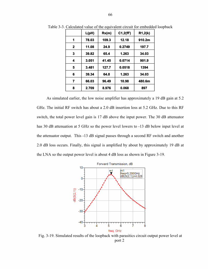
66
Table 3-3. Calculated value of the equivalent circuit for embedded loopback
8970.0688.9762.7098
480.6m10.9896.4966.037
34.031.26364.839.346
13940.0518127.73.4815
901.90.071441.453.0514
34.031.26365.439.823
197.70.274924.911.082
910.2m12.18109.378.031
R1,2(k)C1,2(fF)Rx(m)L(pH)
8970.0688.9762.7098
480.6m10.9896.4966.037
34.031.26364.839.346
13940.0518127.73.4815
901.90.071441.453.0514
34.031.26365.439.823
197.70.274924.911.082
910.2m12.18109.378.031
R1,2(k)C1,2(fF)Rx(m)L(pH)
As simulated earlier, the low noise amplifier has approximately a 19 dB gain at 5.2
GHz. The initial RF switch has about a 2.0 dB insertion loss at 5.2 GHz. Due to this RF
switch, the total power level gain is 17 dB above the input power. The 30 dB attenuator
has 30 dB attenuation at 5 GHz so the power level lowers to -13 dB below input level at
the attenuator output. This -13 dB signal passes through a second RF switch and another
2.0 dB loss occurs. Finally, this signal is amplified by about by approximately 19 dB at
the LNA so the output power level is about 4 dB loss as shown in Figure 3-19.
Fig. 3-19. Simulated results of the loopback with parasitics circuit output power level at
port 2

67
3.5 Measured Results of Loopback Sub-circuits and Test System
The 40 dB, 50 dB, and 60 dB RF attenuators were fabricated with the IBM 0.25
micron SiGe BiCMOS-6HP technology through the MOSIS fabrication service. The
measurements of RF attenuators were performed by using an on-wafer Cascade
Microtech Air Coplanar Probe (ACP) and a HP8510C Network Analyzer. The
photomicrograph of the attenuators is shown in Figure 3-20. The total chip size is about
1.2 mm2 (1.2 mm x 1.0 mm).
Fig. 3-20. Die micrograph (1.0mm x 1.2mm) of the RF attenuator and RF switch
The measured results of the attenuators are shown in Figure 3-21. The transmitted
power at port 2 in the 30 dB attenuator is -28.6 dB, in the 40 dB attenuator is -39.7 dB, in
40 dB Attenuator
50 dB Attenuator
60 dB Attenuator
RF switch

68
the 50 dB attenuator is -49.2 dB, and in the 60 dB attenuator is -57.5 dB at 100 MHz
respectively and this agrees well with the simulated -30.1 dB, -40.1 dB, -50.1 dB, and -
60.1 dB responses. But at high frequency, the 50 dB and 60 dB attenuators are very
ineffective and show poor agreement with simulation indicating significant substrate
signal leakage that exceeds the 50 dB and 60 dB attenuator transmissions. As shown in
Figure 3-21, the leakage power increases at higher frequencies.
Attenuator
-70
-65
-60
-55
-50
-45
-40
-35
-30
1 2 3 4 5 6 7 8 9 10Frequency (GHz)
( dB
)
40 dB ( Simulation )50 dB ( Simulation )60 dB ( Simulation )40 dB ( Measurement )50 dB ( Measurement )60 dB ( Measurement )
Fig. 3-21. Measured results of various pi-type attenuators
As shown in Figure 3-21, RF attenuators are very ineffective at high frequency.
The RF attenuator and silicon substrate can be modeled as shown in Figure 3-22. A
coupling capacitor, Cc is modeled between signal path and substrate. Coupling capacitors
are distributed evenly through the dioxide layer. And silicon substrate can be modeled as
vertical components (Rsub1 and Csub1) and horizontal components (Rsub2 and Csub2). These

69
vertical and horizontal components are distributed evenly also. A portion of the signal on
the pads and attenuator is coupled through coupling capacitor Cc. This signal propagates
to every direction. Some signals propagate to the bottom plate of a silicon substrate and
others propagate to the side through the silicon substrate. A portion of the signal launched
at Pad1 propagates to Pad2 through the coupling capacitor Cc, substrate resistor Rsub2,
and substrate capacitor Csub2. If the leakage power through substrate exceeds the
designed attenuation level, the attenuator becomes very ineffective at high frequency.
SiO2
Si
Cc Cc Cc Cc
Csub1 Csub1
Rsub1
Rsub1Rsub2
Csub2
Pad1 Pad2
Attenuator
Sub-contact
SiO2
Si
Cc Cc Cc Cc
Csub1 Csub1
Rsub1
Rsub1Rsub2
Csub2
Pad1 Pad2
Attenuator
Sub-contact
Fig. 3-22. Model of the RF attenuator and substrate
Two layouts are shown in Figure 3-23. Figure 3-23-a) shows the layout of the RF
attenuator without substrate contacts. This has -30 dB attenuation and its measurement
results show in Figure 3-21. As mentioned earlier, there is some signal leakage through a
substrate and this attenuator is very ineffective at high frequency. To prevent the signal

70
leakage through a substrate, many substrate contacts are used as shown in Figure 3-23-b).
The substrate contacts make a metal wall and block the signal leakage between two signal
ports.
(a) RF attenuator without substrate contacts.
Sub contact Sub contact Sub contactSub contact Sub contact Sub contact
(b) RF attenuator with substrate contacts.
Fig. 3-23. Layout of the RF attenuator with and without substrate contact
The 30 dB RF attenuators without substrate contacts and the 30 dB RF attenuator
with substrate contacts were fabricated with the IBM 0.18 micron SiGe BiCMOS-7WL
technology through the MOSIS fabrication service. The measurement of the 30 dB RF
attenuator was performed by using an on-wafer Cascade Microtech Air Coplanar Probe
(ACP) and a HP8510C Network Analyzer. The photomicrograph of the attenuators is
shown in Figure 3-24. The total chip size is about 1.7 mm2 (1.6 mm x 1.1 mm).

71
Fig. 3-24. Die micrograph (1.6mm x 1.1mm) of the RF attenuator and RF switch
30 dB without sub-contact 30 dB with sub-contact 30 dB without sub-contact 30 dB with sub-contact
ss
30 dB without sub-contact 30 dB with sub-contact 30 dB without sub-contact 30 dB with sub-contact
ss
Fig. 3-25. Measured results of the 30 dB attenuator
The measured results of the attenuators are shown in Figure 3-25. The transmitted
power at port 2 in the 30 dB attenuator with substrate contacts is -29.9 dB at 5 GHz. The
attenuation is very constant and variation is within 0.3 dB up to 10 GHz. It is very
effective and shows good agreement with the simulation when compared to the
measurement result of 30 dB attenuator without substrate contacts.
Without sub-contact
With sub-contact

72
The RF switch was fabricated with the IBM 0.25 micron SiGe BiCMOS-6HP
technology through the MOSIS fabrication service. The measurement of the RF switch
was performed by using an on-wafer Cascade Microtech Air Coplanar Probe (ACP) and a
HP8510C Network Analyzer. The photomicrograph of the attenuators is shown in Figure
3-20. The total chip size is about 1.2 mm2 (1.2 mm X 1.0 mm).
Switch
-60
-50
-40
-30
-20
-10
0
1 2 3 4 5 6 7 8 9 10Frequency (GHz)
( dB
)
Simulaton (SW-on)Simulation (SW-off)Measurement (SW-on)Measurement (SW-off)
Fig. 3-26. Measured results of the RF switch
The measured results of the RF switch are shown in Figure 3-26. The transmitted
power at port 2 is -2.4 dB at 5.2 GHz. The leakage power at port 3 is -16 dB. The
simulated transmitted power at port 2 is -2.0 dB at 5.2 GHz and the simulated leakage
power at port 3 is -32 dB. The measurements show good agreement with simulation. The
leakage power at port 3 is higher than simulation. The two MOSFETs and two resistors
that were removed to save switch area result in this high leakage.
The loopback test structure was fabricated with the IBM 0.25 micron SiGe
BiCMOS-6HP technology through the MOSIS fabrication service. The measurement of
the loopback test structure was performed by using an on-wafer Cascade Microtech Air
Coplanar Probe (ACP) and a HP8510C Network Analyzer. The photomicrograph of the

73
overall loopback test IC is shown in Figure 3-27. The total chip size is about 1.6 mm2
(1.85 mm x 0.87 mm).
Fig. 3-27. Die micrograph (1.85mm x 0.87mm) of the embedded loopback test model
The measured results of the embedded loopback test model are shown in Figure 3-
28. The transmitted power at port 2 is 2 dB at 5 GHz. As mentioned before in Figure 3-
19, the simulated transmitted power at port 2 is 4 dB at 5 GHz and the measurements
show good agreement with simulation.
Measurement
Simulation
Measurement
Simulation
Fig. 3-28. Measured results of the embedded loopback test model
3.6 Conclusions
Attenuators, RF switches, Low Noise Amplifier and loopback test circuits have
been designed and characterized for embedded testing of RF ICs. To realize high

74
performance attenuation at high frequency, a method of reducing leakage through the
substrate is investigated. Making a blocking wall using substrate contacts is shown to be
a good method to reduce the substrate leakage. The measurement results of 30 dB RF
attenuator with substrate contacts show better high frequency performance than the
measurement results of an RF attenuator without substrate contacts. Using this method,
RF attenuator is close to the design specification up to 10 GHz.
Compared with a traditional RF switch, a new test RF switch is realized with half
the area by reducing the design by two transistors as shown in this chapter. The RF
switch was designed for minimum insertion loss using the optimum gate dimension (the
optimum gate width and the minimum gate length). The measurement results showed
good agreement with simulation.
For the experiments with the loopback test, the parasitics of metal lines for
interconnection are modeled and considered in simulation to improve accuracy. There are
closer agreements between the simulation and the measurement results when parasitics
are considered. Through this research, the loopback test method was proposed and
verified for TDD (Time Division Duplex) communication methods up to 5 GHz.
This is the first attempt for embedded loopback test of a wireless communication system.
This proposed loopback was designed with minimum area (0.02 mm2) and can extend the
application frequency as high as the operating frequency of the on-chip RF attenuator and
RF switch. The attenuation value for the loopback signal can be decided according to
each design application.

75
CHAPTER 4 ANOTHER EMBEDDED LOOPBACK FOR RF ICS TEST
4.1 Introduction
The loopback test, as proposed in an earlier chapter, is one of the least expensive
test methods for verifying functionality in a communication circuit. However, this “go”
or “no go” test gives little insight into circuit failure mechanisms and is of little assistance
in debugging a circuit manufacturing process. On-chip loopback techniques may prove
attractive when doing bare die tests for ICs in system-in-a-package and when the chip
package introduces parasitics that adversely effect the off-chip short necessary for
loopback test. This can occur with very high frequency transceivers in the > 10 GHz
range.
SYNTH
RX BLOCK
RF S/W
ANT
HPA
LNA
BPF AMP
AMP
AGCAMP
AMPBPF
TX BLOCK
MIXER
MIXER
ATT
Coupler
RF S/W
Power Monitor
Test Circuit for Embedded testing
SYNTH
RX BLOCK
RF S/W
ANT
HPA
LNA
BPF AMP
AMP
AGCAMP
AMPBPF
TX BLOCK
MIXER
MIXER
ATT
Coupler
RF S/W
Power Monitor
Test Circuit for Embedded testing
Fig. 4-1. Block diagram of another embedded loopback RFIC test

76
In a previous chapter, the loopback test named Type 1 was proposed for High
Power Amplifiers (HPA), that was built using a different power amplifier technology
(GaAs) that is separate from the silicon IC transceiver block.
In this chapter, another embedded loopback test named Type 2 will be examined.
As mentioned earlier, the Type 1 test is effective for separated high power amplifier
(HPA) designs using different materials for the HPA design. The biggest difference
between Type 1 and Type 2 is that the later is for single chip design including the HPA in
the same wafer. Designing the whole system function in a single chip is a new design
trend. Figure 4-1 shows a WLAN block diagram of the loopback Type 2 test in which
transmitter signals test the receiver by connecting them to the receiver through RF
switches with an attenuator in the signal path.
The HPA connects to the antenna (ANT) through the RF switch (RF S/W). In this
loopback test example, test signals are amplified via a high power amplifier (HPA) and
most signals are delivered to the antenna input port though a directional coupler and RF
switch. Further, some of the coupled signals are delivered to the loopback attenuator
through a first RF switch and then an LNA via a second RF switch. The LNA requires a
weak input signal created by the attenuator in the loopback signal path. Also, the HPA
power can be monitored via a power detector. The loopback signal path is shown in the
shaded region of Figure 4-1. In summary, Figure 4-1 shows the necessary circuits for
demonstrating the transceiver RF embedded loopback test signal path: these consist of an
HPA (high power amplifier), a directional coupler, a RF switch, an attenuator, a second
RF switch, peak detector, and a LNA.

77
4.2 Design of Loopback Circuit Type 2
The embedded loopback circuit is modeled with an HPA (high power amplifier), a
directional coupler, a RF switch, an attenuator, a second RF switch, peak detector, and a
LNA as shown in Figure 4-2.
HPA
LNA
ATT
Coupler
RF S/W 1
Power Detector
Port 1 Port 2
Port 3Port 4
RF S/W 2
Port 5
HPA
LNA
ATT
Coupler
RF S/W 1
Power Detector
Port 1 Port 2
Port 3Port 4
RF S/W 2
Port 5
Fig. 4-2. The block diagram of embedded loopback test model Type 2
The key test circuits for implementing embedded loopback test Type 2 are high-
frequency attenuators, which reduce the transmitted signal to sufficiently low test signal
values, and RF switches, which are used to modify the signal path between test operation
and normal operation. The resistor-based attenuator [Poz97][Viz95] was selected as the
most suitable for embedded loopback RFIC test because it has wideband circuit operation
and compact implementation. The 30 dB attenuator is designed according to the Table 4-
1.
The second key component for the embedded loopback RFIC test is the RF switch.
Two n-MOSFET and two control resistors are used for the RF switch as shown in Figure
4-6. For optimum size, the minimum gate length 180 nM is used and the gate width is

78
designed as 4.23 uM with 30 fingers. To realize the loopback test Type 2, two additional
amplifiers, a directional coupler and a power detector are needed. One is a low noise
amplifier (LNA) and another is a high power amplifier (HPA) as shown in Figure 4-2. A
cascode low noise amplifier is designed as a low noise amplifier. The schematic diagram
is shown in Figure 4-3. The transistor size is designed for optimum gain and noise figure.
For input matching, two spiral inductors are used: 1.08 nH and 220 pH as shown in
Figure 4-3. Similarly, for output matching, two spiral inductors and three MIM capacitors
are used as shown in Figure 4-3.
Bias Network
Vdd
1.94 nH
600 fF
7x
13x
3.0 pF
220 pH
1.08 nH
5.0 pF
3 k
3 k
Output Matching
Input Matching
999 fF
2.40 nH
600 fFBias Network
Vdd
1.94 nH
600 fF
7x
13x
3.0 pF
220 pH
1.08 nH
5.0 pF
3 k
3 k
Output Matching
Input Matching
999 fF
2.40 nH
600 fF
Fig. 4-3. The schematic of cascode low noise amplifier (LNA)
A 10-dB directional coupler [Yoo04] is designed for 5 GHz operation as shown in
Figure 4-4. This 10-dB directional coupler employs six spiral inductors and five
capacitors. Each design value equation is derived in chapter 3.

79
Port 1 Port 3
Port 2 Port 4
445 fF
1.08 nH
4.71 nH
445 fF
445 fF445 fF
420 fF
1.08 nH
1.08 nH 1.08 nH
4.71 nH
Port 1 Port 3
Port 2 Port 4
445 fF
1.08 nH
4.71 nH
445 fF
445 fF445 fF
420 fF
1.08 nH
1.08 nH 1.08 nH
4.71 nH
Fig. 4-4. The schematic of 10 dB directional coupler
4.3 Simulation of Loopback Sub-circuits and System Type 2
Cadence SpectreS was used to design 5 GHz 30 dB lumped passive π-type
attenuators. As shown in Figure 4-5, at 5 GHz the simulation results for the magnitude at
port 2 for the 30 dB attenuator is approximately -30.1 dB. This simulation includes
parasitic parameters (capacitances) of the P+ Polysilicon resisters which degrade high
frequency response.
Finally, the dimension of the n-MOSFET RF switch is decided for optimum value
according to various simulation results. As mentioned earlier, the minimum gate length is
better for insertion loss and increasing the gate width is not always good. The simulated
optimum insertion loss of this n-channel MOSFET is 0.6 dB when the number of fingers
is 30, the gate length is 180 nM, and the layout gate width is 4230 nM as shown in Figure
4-5.

80
-0.6 dB-0.6 dB
Fig. 4-5. Simulated results of the RF switch
12
3
4
5
6
7
8
9
10111213
1415
16
17
18
192021
22
23242526 27 28
4
5
6
7
8
9
4
5
6
7
8
9
4
5
6
7
8
9
4
5
6
7
8
9
4
5
6
7
8
9
4
5
6
7
8
9
4
5
6
7
8
9
4
5
6
7
8
9
4
5
6
7
8
9
4
5
6
7
8
9
4
5
6
7
8
9
4 7
13
16
17
18
19
13
16
17
18
19
13
16
17
18
19
13
16
17
18
19
13
16
17
18
19
16
18
12
3
4
5
6
7
8
9
10111213
1415
16
17
18
192021
22
23242526 27 28
4
5
6
7
8
9
4
5
6
7
8
9
4
5
6
7
8
9
4
5
6
7
8
9
4
5
6
7
8
9
4
5
6
7
8
9
4
5
6
7
8
9
4
5
6
7
8
9
4
5
6
7
8
9
4
5
6
7
8
9
4
5
6
7
8
9
4 7
13
16
17
18
19
13
16
17
18
19
13
16
17
18
19
13
16
17
18
19
13
16
17
18
19
16
18
Fig. 4-6. The schematic of cascode low noise amplifier with parasitics for Type 2

81
The schematic of this cascode low noise amplifier with parasitics is shown in
Figure 4-6. Every single metal line for connection between transistors is modeled as an
equivalent circuit as shown in Figure 3-22. All parasitics in the single metal line, as
shown in Figure 4-6, are calculated by the EM simulator ASITIC [Nik00] which was
developed by Berkeley and each value is shown in Table 4-1.
Table 4-1. Calculated value of the equivalent circuit for LNA of Type 2
748.732.528
15.26231.412.082.9127
33.41867126.750.0726
0.5651,22374.328.4225
538.886.229.678.3024
32.943223
36.741622
130250.290.13.7621
132751.852.252.8020
135450.1112.54.9919
370518.571.392.2018
135749.9112.24.8317
84228.173.441.3516
0.84213,54015
1.15310,59014
222928.12674.0513
91674.1116.95.3212
44.741711
919.974.874.334.8010
206632.81524.329
205533.690.314.148
216930.871.122.207
132.5220.56
174139.198.84.025
84228.171.461.3344
536.683.848.2911.493
510117.923.0311.232
512.5102.215.595.5641
R1,2(k)C1,2(aF)Rx(m)L(pH)

82
Finally, the simulation result of the low noise amplifier with parasitics is shown in
Figure 4-7. The simulated gain (S21) is 16.3 dB at 5.0 GHz and reflection at input and
output ports are lower than -10 dB at 5.0 GHz.
S21(dB)
S22(dB)
S11(dB)
S21(dB)
S22(dB)
S11(dB)
Fig. 4-7. S-parameter simulation result of the low noise amplifier with parasitics for Type 2
5
8
11
14
17
20
-30 -25 -20 -15 -10 -5 0 5
Pin (dBm)
Gai
n (d
B)
Fig. 4-8. Gain simulation result of the low noise amplifier with parasitics for Type 2

83
The schematic of the lumped passive directional coupler with parasitics is shown in
Figure 4-9. Every single metal line for connection between lumped passive components
is modeled into equivalent circuits as shown in Figure 3-22. All parasitics in the single
metal line, as shown in Figure 4-9, are calculated by EM simulator ASITIC which was
developed by Berkeley and each value is shown in Table 4-2.
Fig. 4-9. The schematic of lumped passive directional coupler with parasitics for Type 2
Table 4-2. Calculated value of the equivalent circuit for directional coupler of Type 2
0.03222.64141.799.645
0.03222.64143.7101.44
0.6831.4311.024.943
4762.35110.638.92
492.30.1229.626.591
R1,2(k)C1,2(fF)Rx(m)L(pH)
0.03222.64141.799.645
0.03222.64143.7101.44
0.6831.4311.024.943
4762.35110.638.92
492.30.1229.626.591
R1,2(k)C1,2(fF)Rx(m)L(pH)

84
Finally, the simulation results for the lumped passive directional coupler is shown
in Figure 4-10. The simulated coupling (S21) is -10.37 dB at 5.0 GHz and simulated
through (S31) is -1.47 dB at 5.0 GHz. The simulated reflection ratios (S11,S22, and S33) of
each port are lower than -20 dB at 5 GHz.
Fig. 4-10. S-parameter simulation result of the directional coupler with parasitics for
Type 2
As shown in Figure 4-2, the embedded loopback circuit is modeled with an HPA
(high power amplifier), a directional coupler, a RF switch, an attenuator, a second RF
switch, a peak detector, and a LNA. Similarly, every single metal line for connection is
modeled into equivalent circuits as shown in Figure 3-22. All parasitics in single metal
plates as shown in Figure 4-11 are calculated by EM simulator ASITIC which was
developed by Berkeley and each value is shown in Table 4-3.

85
LNA
LNA
RF S/W RF S/W
ATT
Coupler
Power Detector
LNA
LNA
RF S/W RF S/W
ATT
Coupler
Power Detector
Fig. 4-11. The block diagram of embedded loopback test model Type 2 with parasitics
Table 4-3. Calculated value of the equivalent circuit for the embedded loopback Type 2
43.560.8837.9622.65V2-3
74.094.3170.4251.24V2-2
1.05225.23203.8199.9V2-1
R1,2(k)C1,2(fF)Rx(m)L(pH)
43.560.8837.9622.65V2-3
74.094.3170.4251.24V2-2
1.05225.23203.8199.9V2-1
R1,2(k)C1,2(fF)Rx(m)L(pH)
As simulated before, the low noise amplifier has approximately 16.3 dB gain at 5.2
GHz. The through port of the directional coupler has about a 1.5 dB insertion loss at 5.2
GHz. Due to this directional coupler, total power level gain at port 2 is 14.7 dB above the
input power as shown in Figure 4-12-dB(S(21)). The coupling port of the directional
coupler has about a 10.4 dB insertion loss at 5.2 GHz. The RF switch has about a 1.0 dB
insertion loss at 5.2 GHz. The 30 dB attenuator has a 30 dB attenuation at 5.2 GHz.

86
Finally, simulation results of total loop back test Type 2 are shown in Figure 4-12. Total
power level gain at port 3 is -15.2 dB below the input power as shown in Figure 4-12-
dB(S(31)). The reflection ratio of each port (port 1, port 2, and port 3) is lower than -10
dB at 5.2 GHz as shown in Figure 4-12.
Fig. 4-12. Simulated results of the loopback Type 2 with parasitics
4.4 Measured Results of Loopback Test Type 2 System
The loopback test Type 2 structure was fabricated with the IBM 0.18 micron SiGe
BiCMOS-7WL technology through the MOSIS fabrication service. The measurement of
the loopback test Type 2 was performed by using an on-wafer Cascade Microtech Air
Coplanar Probe (ACP) and a HP8510C Network Analyzer. The photomicrograph of the
overall loopback test Type 2 IC is shown in Figure 4-13. The total chip size is about 1.9
mm2 (1.6 mm X 1.2 mm).

87
Fig. 4-13. Die micrograph (1.6mm x 1.2mm) of the embedded loopback test model
The measured results of the embedded loopback test model are shown in Figure 4-
14. The loopback power level gain at LNA input is -15 dB at 5.2 GHz. As mentioned
before in Figure 4-12, the simulated loopback power level gain at LNA input is -15.2 dB
at 5.2 GHz and shows good agreement with measurement. The transmitted power at port
2 is 12 dB at 5.2 GHz. As mentioned before in Figure 4-12, the simulated transmitted
power at port 2 is 14.7 dB at 5.2 GHz and shows good agreement with measurement.
Simulation- dB(S(2,1)) Simulation- dB(S(3,1))X Measurement - dB(S(3,1)) Measurement -dB(S(2,1))
Simulation- dB(S(2,1)) Simulation- dB(S(3,1))X Measurement - dB(S(3,1)) Measurement -dB(S(2,1))
Fig. 4-14. Measured results of the embedded loopback test Type 2 model

88
4.5 Conclusions
Attenuators, RF switches, directional couplers, peak detector, low noise amplifiers
and loopback test Type 2 circuits have been designed and characterized for embedded
test of RF ICs. The loopback test Type 2 includes a directional coupler and a peak
detector. Therefore, the Type 2 loopback test is effective for a single chip design
including the HPA in the same IC. To the author’s best knowledge, this is the first
attempt for embedded loopback test of wireless communication system. As mentioned in
a previous chapter, the parasitics of metal lines for interconnection are modeled and
considered for simulation. The measured results of the loopback power level gain at LNA
input are -15 dB at 5.2 GHz. As mentioned before in Figure 4-12, the simulated loopback
power level gain at LNA input is -15.2 dB at 5.2 GHz. There is closer agreement between
the simulation and the measurement results with the metal line parasitics included than
without parasitic consideration. The attenuation value and coupling value of the
directional coupler can be decided according to each transceiver test application.

89
CHAPTER 5 EMBEDDED S-PARAMETER MEASUREMENT MODULE
5.1 Introduction
Modern integrated systems include dense ICs containing diverse circuits such as
microprocessors, memory, digital processing blocks, analog functional blocks, and RF
functional blocks. As systems-on-a-chip (SoCs) become more advanced and complex, it
is necessary to reduce manufacturing costs, especially testing costs. There are many types
of test, including bench test for circuit verification and manufacturing test for individual
part verification. Manufacturing test must be done efficiently to keep part cost low. The
test goal is to remove bad parts. Test equipment specifications can often be relaxed as
compared to bench characterization equipment.
To verify the performance of SoCs, mixed-signal and RF testing may be used.
Among these test methods, RF test is a major part of the entire test cost. RF measurement
specifications often require the comparison of the amplitude and the phase difference
between an unknown signal and a reference signal. The magnitude and phase verification
of an RF channel determines whether a part can be sold or not.
The s-parameters are considered a good method for the bench characterization of
RF and microwave components because they provide vector data from a controlled and
easily achievable 50 Ω impedance system. To perform this measurement, a direct and
accurate measurement is needed and a de-embedding procedure is adopted to remove the
testing fixture characteristics from the overall measurement.

90
As previously mentioned, testing and verification are a major part of the total
production IC testing cost for RF and microwave components. This is so because costly
RF and microwave test equipment (vector network analyzers or equivalent) are required.
Other testing costs include the long time required to set up and calibrate test equipment.
Only the most expensive automated test equipment (ATE) has s-parameter capability and
it is too costly to use for low cost consumer parts.
Over the years, various methods have been considered to reduce testing costs
[Koo91][Pla95]. One of these methods is on-chip measurement [Cow01]. Embedded test
methods can mathematically subtract the effects of parasitics caused by the contact pads,
the interconnections between the pads, RF probes and RF cables for connection to test
equipment. At RF microwave frequencies, unmodeled parasitics cause significant errors
in parametric data. A complex calibration procedure is needed to subtract the unwanted
parasitic effects. Also, costly testing equipment is needed to measure RF performance.
For this reason, an embedded test method for RF SoCs is potentially a very economical
method for maintaining a high level test accuracy. The use of on-chip s-parameter
techniques for IC production test is limited by area and cost considerations. However, the
design of single chip s-parameter test modules allows for extremely low cost s-parameter
test probes and also low cost multi-channel RF test boards in automated test. Future
applications of radio imagining array circuits for automobiles at 77 GHz may require on-
chip sensor verification. In these systems, having an on-chip s-parameter measurement
capability nearby may prove invaluable in circuit performance verification and
calibration. In addition, on-chip s-parameter test ICs can be used on the load board of an
ATE system.

91
Table 5-1 is the summary of specifications of a traditional and the proposed on-chip
network analyzer. As we know, network analyzers that have been sold in the commercial
market have a very high phase accuracy and high magnitude accuracy. For example, the
Agilent PNA network analyzer E8363B measurement accuracy is within 0.1 dB
magnitude and 1º phase. To get this sensitivity, the traditional network analyzer needs a
large enclosure to add very accurate RF/microwave test blocks, thereby adding cost of the
analyzer.
Table 5-1. Specification of the commercial network analyzer and on-chip s-parameter module
2 or more2 or 4Number of test ports
4˚1˚Measurement uncertainty (Phase)
0.5 dB0.1 dBMeasurement uncertainty (Magnitude)
On-chip s-parameter module
Traditional Network Analyzer (E8363B)
2 or more2 or 4Number of test ports
4˚1˚Measurement uncertainty (Phase)
0.5 dB0.1 dBMeasurement uncertainty (Magnitude)
On-chip s-parameter module
Traditional Network Analyzer (E8363B)
The on-chip s-parameter measurement method occupies a small area and measures
s-parameters directly (without any probing). That is why the on-chip method provides
major advantages in cost and time when the chip is embedded in probes and placed on
multi-channel RF test boards. Again, there are cost trade offs in integrating these systems
on every SoC. But sharing an on-wafer s-parameter test system in the wafer scribe lanes
may probe advantageous for production IC test. There are huge difficulties in achieving
the same performance on-chip as a commercial big network analyzer. Our measurement
accuracy is within 0.5 dB with magnitude and 4º phase. Even though there is
performance degradation for on-chip s-parameter realizations, test time may be reduced

92
which saves significant manufactured IC part cost. The goal is to make the test accurate
enough for verification test of production ICs.
5.2 Introduction of Scattering Parameters
For RF microwave measurements, using s-parameters is advantageous over other
parameters including y, z, and h-parameters. S-parameters are defined in terms of voltage
traveling waves, which are relatively easy to measure in a microwave system while y, z,
and h-parameters require open and short circuits which are often not feasible.
i(x,t)
v(x,t)+
-
xx
i(x,t)
v(x,t)+
-
xx
(a) Transmission line for an incremental length
i(x,t)
v(x,t)+
-x
Rx
Lx
Gx Cx
i(x+x,t)
+
-
v(x+x,t)
i(x,t)
v(x,t)+
-x
Rx
Lx
Gx Cx
i(x+x,t)
+
-
v(x+x,t)
(b) Lumped-element equivalent circuit
Fig. 5-1. Transmission line and equivalent circuit

93
Another strong advantage is that each parameter has a very similar meaning
compared to other parameters; for example S11 is a reflection ratio at port 1. S22 is also a
reflection ratio at port 2. S21 and S12 show gain or loss between two ports. The greatest
advantage of using s-parameter for RF microwave measurement is that multiple devices
can be cascaded and an overall system performance easily estimated. In addition, case of
calibration and high accuracy are the main reason why the s-parameters are so popular for
RF and microwave measurement.
For more accurate s-parameter description, transmission line theory is adopted
instead of circuit theory [Poz97][Gon97].
As shown in Figure 5-1, a transmission line can be modeled with a lumped-element
equivalent circuit. Voltage and current waves travel through a transmission line so the
magnitude and phase of voltage and current can vary according to their length. The
voltage and current is given by
V(z) = V+ e-jβx + V- ejβx (5.1)
I(z) = I+ e-jβx - I- ejβx (5.2)
When x=0, at the n th port, the total voltage and current become
Vn = Vn+ + Vn
- (5.3)
In = In+ - In
- (5.4)
The scattering matrix is a ratio of the incident voltage wave to those reflected. In
the n-port network, Vn+ is the amplitude of the incident voltage wave at port n, and Vn- is
the amplitude of the reflected voltage wave at port n. As previously stated, the s-
parameter is defined as a ratio of these incident and reflected voltage waves. So the s-
parameter can be defined as equation (5.5) and (5.6)

94
⎥⎥⎥⎥⎥⎥⎥
⎦
⎤
⎢⎢⎢⎢⎢⎢⎢
⎣
⎡
⎥⎥⎥⎥⎥⎥
⎦
⎤
⎢⎢⎢⎢⎢⎢
⎣
⎡
=
⎥⎥⎥⎥⎥⎥⎥
⎦
⎤
⎢⎢⎢⎢⎢⎢⎢
⎣
⎡
+
+
+
−
−
−
nnn v
v
v
S
SS
v
v
v
.
.
S . . S ..
S . . S S . . S
..
2
1
nnn21
2n2221
1n1211
2
1
(5.5)
jkfor 0 j
-i
VV
≠=
++
=kV
ijS (5.6)
Assume that the network has an n-port where Zon is the characteristic impedance of
the nth port, and Vn+ and Vn- are defined as incident and reflected voltage wave at port n
respectively. A new set of wave equations is defined to explain a physically meaningful
power relation in terms of wave amplitudes as shown in Figure (6-7) (6-8).
( ) I z vz21 I z v n0nn
0n0n0n +=== ++
nn za (5.7)
( )n0nn0n
0n0n I z vz21 I z- v −=== −−
nn zb (5.8)
So, equation (5.7) (5.8) become
( ) az V V n0nnn nn bV +=+= −+ (5.9)
( ) ( ) az1 V V
z1 n
0nnn
0nn bI −=−= −+ (5.10)
Rewrite equation (5.5) with equation (5.7)(5.8),
[ ] [ ][ ] a s =b (5.11)
where the i,j th element of the scattering matrix is given by
jkfor 0 j
-i
ab
≠=
++
=ka
ijS (5.12)

95
This concept is described in Figure 5-2. In this figure, each traveling wave at the
port has a direction where an represents an incident wave at the nth port, and bn represents
a reflected wave from that port. When a power wave is launched at port 1, a portion of
the wave energy will be reflected and the rest of the energy will be transmitted. The same
is true with measuring energy at port 1. When a power wave is launched at port 2, some
of the wave energy will be transmitted to the port 1 and there rest of the wave energy will
be reflected at port 2.
Incident Transmitted
Reflected Reflected
Transmitted Incident
DUTPort 1 Port 2
a1
b1 a2
b2
S21
S12
S22S11
Incident Transmitted
Reflected Reflected
Transmitted Incident
DUTPort 1 Port 2
a1
b1 a2
b2
S21
S12
S22S11
Fig. 5-2. Function diagram of s-parameter
The s-parameter then becomes
1port at power waveincident 1port at power wave reflected
01
111
2
===aa
bS (5.13)
1port at power waveincident 2port at power wave dtransmitte
01
221
2
===aa
bS (5.14)
2port at power waveincident 1port at power wave dtransmitte
02
112
1
===aa
bS (5.15)

96
2port at power waveincident 2port at power wave reflected
02
222
1
===aa
bS (5.16)
5.3 Introduction of Mixed Mode Scattering Parameter
Differential circuits have performed critical roles in an RF and microwave circuit
design as well as in analog circuit design. Mixed mode scattering parameters have been
investigated for mixed mode circuit analysis [Bok95]. The basic concept of mixed mode
signals in a two-port network is shown in Figure 5-3.
DUT∆ V1 ∆ V2
Port 1 Port 2
DUT∆ V1 ∆ V2
Port 1 Port 2
Fig. 5-3. Signal diagram of mixed mode two-port network
As shown in Figure 5-3, the differential-mode signal definition is that two voltage
and current waves flow through the pair lines with different phases. So the voltage and
current flow has a magnitude (∆V1≠ 0, ∆V2≠ 0). According to this definition, it is very
difficult for the signal to be referenced to a ground potential. It is better that each two
signals on both pairs of lines are referenced to each other.
On the other hand, the common-mode signal definition is that two voltage and
current waves flow through the pair of lines with the same magnitude and phase. So the
voltage and current waves on both line pairs are equal in phase and in magnitude with
respect to ground, so a differential voltage and current has no magnitude. (∆V1= 0, ∆V2=
0)

97
For the mixed mode s-parameter, the differential mode voltage and current and the
common mode voltage and current should be defined. The differential mode voltage is
( ) 21 vvxvdm −≡ (5.17)
The differential mode current can be defined
( ) ( ) 21
21 iixidm −≡ (5.18)
The common mode voltage and current also can be defined same way
( ) ( ) 21
21 vvxvcm +≡ (5.19)
( ) 21 iixicm +≡ (5.20)
The characteristic impedance of the differential and common mode at some point x
also can be described
( )( )
( )( )
22
oo
poso
poso
posdm
posdm
dm ZZxvxv
xixv
Z ==≡ (5.21)
( )( )
( )( )( ) 22
e
epose
pose
poscm
poscm
cmZ
Zxvxv
xixv
Z ==≡ (5.22)
The new mixed mode wave equation at port1 can be derived using the new
definition of mixed mode voltage, current, and characteristic impedance. (Assume the
port 1 is located at x=o)
( ) ( )[ ] 01 2
1=+= xdmdmdm
dmdm Rxixv
Ra (5.23)
( ) ( )[ ] 01 2
1=−= xdmdmdm
dmdm Rxixv
Rb (5.24)

98
( ) ( )[ ] 01 2
1=+= xcmcmcm
cmcm Rxixv
R (5.25)
( ) ( )[ ] 01 2
1=−= xcmcmcm
cmcm Rxixv
Rb (5.26)
The conceptual diagram of the mixed-mode two-port is shown in Figure 5-4.
Differential-mode ports
Common-mode ports
Physical port 1
Physical port 2
adm1
bdm1
acm1
bcm1
bdm2
adm2
bcm2
acm2
Mixed-mode
2-ports
Differential-mode ports
Common-mode ports
Physical port 1
Physical port 2
adm1
bdm1
acm1
bcm1
bdm2
adm2
bcm2
acm2
Mixed-mode
2-ports
Fig. 5-4. Conceptual diagram of mixed-mode two-port
Rewrite (5.11) using equation (5.23), (5.24), (5.25), and (5.26)
2141132121111 cmcmdmdmdm asasasasb +++= (5.27)
2241232221212 cmcmdmdmdm asasasasb +++= (5.28)
2341332321311 cmcmdmdmcm asasasasb +++= (5.29)
2441432421412 cmcmdmdmcm asasasasb +++= (5.30)
2
1
2
1
2
1
2
1
⎥⎥⎥⎥
⎦
⎤
⎢⎢⎢⎢
⎣
⎡
⎥⎥⎦
⎤
⎢⎢⎣
⎡=
⎥⎥⎥⎥
⎦
⎤
⎢⎢⎢⎢
⎣
⎡
cm
cm
dm
dm
cccd
dcdd
cm
cm
dm
dm
aaaa
ss
ss
bbbb
(5.31)

99
Where [Sdd] is the differential mode s-parameter, [Scc] is the common mode s-
parameter, and [Scd][Sdc] are the mode conversion or cross mode s-parameters.
5.4 Design for On-Chip Scattering Parameter Measurement
A traditional block diagram for s-parameter measurements is shown in Figure 5-5.
When a power wave is launched at port 1, most of the incident wave energy will be
delivered to the DUT (Device-Under-Test) through the transmit port of the directional
coupler 1. A small amount of the launched wave will be delivered to the receiver 2
through the coupling port of directional coupler 1. When incident power wave is traveling
from the direction coupler 1 to the DUT, some energy is transmitted to the DUT and the
rest is reflected. These reflected power waves from the DUT will travel through the
directional coupler 1 again and be transferred to the receiver 1. Power wave energy
arriving at the DUT will be delivered to port 2 through the directional coupler 2. Minimal
wave energy will be coupled through the coupling port of the directional coupler 2. That
wave energy will be delivered to receiver 4. In addition, when the power wave energy is
launched at port 2, some transmitted energy will be delivered to the receiver 1 and the
rest of the reflected energy wave will be sampled at the receiver 4.
Up to now, the discussion has focused on how power waves are delivered to the
receiver. The receiver of a traditional radio system is composed of an adjustable
attenuator, mixer, LO (Local Oscillator), BPF (Band Pass Filter), and ADC/DSP
(Analog-to-Digital Converter / Digital Signal Processor), as shown in Figure 5-6. It also
includes RF switch blocks, such as an RF switch and a 50Ω terminator that share the
local oscillator but these RF switch blocks are not examined in this phase. At first,
traveling waves, which arrive at the receiver, have suitable levels of strength through the
RF attenuator. These waves convert to base-band signals through the mixer.

100
DUTDirectional Coupler 1
Directional Coupler 2
RECEIVER1
Port 1 Port 2a1b1 a2 b2
RECEIVER2 RECEIVER3 RECEIVER4
DUTDirectional Coupler 1
Directional Coupler 2
RECEIVER1
Port 1 Port 2a1b1 a2 b2
RECEIVER2 RECEIVER3 RECEIVER4
Fig. 5-5. Traditional block diagram for s-parameter measurement
The local oscillator is set to the desired frequency used for down-conversion of
traveling waves at the mixer. The down-converted energy to be analyzed as the signal
arrives at the ADC/DPS through the BPF, and the other energy not useful for test is
eliminated by the BPF. Finally, these desired waves will change to digital signals and
analyzed by DSP. The DSP design is out of scope of this dissertation.
AdjustableAttenuator ADC/DSP
MixerBPF
LO
From Coupler Adjustable
Attenuator ADC/DSP
MixerBPF
LO
From Coupler
Fig. 5-6. Receiver block diagram of traditional s-parameter measurement
As shown in Figure 5-5 and Figure 5-6, a traditional s-parameter measurement
method used a DSP at base-band that can support accurate characterization. A serious

101
disadvantage is that the LO should have high degree of phase noise and be stability. This
requires a large, accurate and energy expensive LO.
In this work, an embedded s-parameter measurement method is proposed. As
depicted in Figure 5-7, a directional coupler is located between each port and the DUT.
The directional coupler passes some wave energy in a forward direction and some wave
energy is coupled to a forward coupling port. If the power wave travels in the reverse
direction, some wave energy is delivered in the reverse direction and wave energy is
coupled to the reverse coupling port. The magnitude and phase of each delivered waves is
measured directly at RF microwave frequencies. By doing this, the highly accurate LO
can be removed from the block diagram of Figure 5-6. Additionally, the parasitic effects
caused by both the probe pads and lines connecting the pad and the DUT can also be
ignored.
Phase Detector 1
DUTDirectional Coupler 1
SW(DPDT) 1
Peak Detector 1
Divider 150Ω
Directional Coupler 2
Phase Detector 2
SW(DPDT) 2
Peak Detector 2
Divider 250Ω
Port 1 Port 2
Phase Detector 1
DUTDirectional Coupler 1
SW(DPDT) 1
Peak Detector 1
Divider 150Ω
Directional Coupler 2
Phase Detector 2
SW(DPDT) 2
Peak Detector 2
Divider 250Ω
Port 1 Port 2
Fig. 5-7. Conceptual block diagram for on-chip s-parameter measurement
Network analyzers sold in the commercial market have a very high degree of
accuracy and dynamic range. For example, their dynamic range is over 120 dB and their

102
measurement accuracy is within 0.1 dB or 1°. To get this sensitivity, the network
analyzer needs a large enclosure and complex circuitry to realize extremely accurate and
high dynamic range functional blocks, thereby greatly increasing the price of the
analyzer. Calculation plays a vital role in measurement accuracy since microwave
fixtures, connectors, cables, probes, and transmission lines can severely degrade the DUT
measurement data. The proposed embedded s-parameter measurement method occupies
minimal chip space and directly measures s-parameters without probing. That is why the
proposed method provides major advantages in cost and time when compared to the
traditional method. Granted, it is difficult to achieve the same performance as big,
commercial network analyzers. However, with minimal performance degradation,
expensive test equipment can be eliminated and test time can be reduced. This is also
useful for the verification test of production ICs.
Port 1 Port 3
Port 2 Port 4
CeCe
Ce Ce
Le Le
Le Le2Lo Co 2Lo
Port 1 Port 3
Port 2 Port 4
CeCe
Ce Ce
Le Le
Le Le2Lo Co 2Lo
Fig. 5-8. The schematic of 10 dB directional coupler for 10 GHz
As shown in Figure 5-5, the traditional network analyzer has four receiver blocks.
Two of them analyze an incident power wave at each port and the other two analyze the
reflected power wave at each port. But in this proposed embedded s-parameter
measurement method, two receiver blocks can be reduced as shown in Figure 5-7. The

103
key sub circuits for implementing embedded s-parameter measurement are directional
couplers, double pole double throw (DPDT) switches, RF power dividers, peak detectors,
and phase detectors as shown in Figure 5-7.
A 10-dB directional coupler [Yoo04] is designed for 10 GHz as shown in Figure 5-
8. For the 10-dB directional coupler, six spiral inductors and five capacitors are used.
Each equation used to decide the design value is derived in chapter 3.
Input 1
M1 M2
R1 R2
Control
Input 2
M4 M3
R4 R3
Output 1
Output 2
R5
_______Control
DC Bias 2
DC Bias 1 R6
Input 1
M1 M2
R1 R2
Control
Input 2
M4 M3
R4 R3
Output 1
Output 2
R5
_______Control
DC Bias 2
DC Bias 1 R6
Fig. 5-9. The schematic of DPST switch for 10 GHz
The DPDT (Double Pole Double Throw) switch is designed for 10 GHz as shown
in Figure 5-9. For the DPDT switch, four n-MOS transistors and seven poly resistors are
used. Each equation used to decide the design value is derived in chapter 4. As mentioned
earlier, the directional coupler is bi-directional. First, the forward direction is defined so

104
that the signal is launched at port 1 as shown in Fig 6-8, the main signal is delivered to
port 3 (forward through port). Second, the designed coupling signal is delivered to port 2
(forward coupling port). Third, no power will be delivered to port 4 (forward isolation
port). One the other hand, the reverse direction is defined such that the signal is launched
at port 3 and then the main signal is delivered to the port 1 (reverse through port). Next,
the sampled coupling signal is delivered to the port 4 (reverse coupling port). Ideally, no
signal will be delivered to the port 2 (reverse isolation port). The port 2 (forward coupling
and reverse isolation) and port 4 (forward isolation and reverse coupling) of the
directional coupler as shown in Figure 5-8 are connected at input 1 and input 2 of DPDT
(Double Pole Double Throw) switches respectively. Therefore, when a signal is launched
with forward direction, the coupled signal is delivered to the input 1 of DPDT switch
through the port 2 (forward coupling). The signal is then forwarded to the output 1 of
DPDT switch for s-parameter measurement. In this case, the control signal is high.
Simultaneously, the other port, port 4 (forward isolation), is connected to the input 2 of
DPDT switch and this port is terminated with 50 Ω resistor through the output 2 of DPDT
switch. On the other hand, during the reverse directional case, the signal is launched at
the port 3 with reverse direction. The coupled signal is delivered to the input 2 of DPDT
switch through the port 4 (reverse coupling). This signal is delivered to the output 1 of
DPDT switch for s-parameter measurement. Here, the control signal is low.
Simultaneously, the other port, port 2 (reverse isolation), is connected to the input 2 of
DPDT switch and this port is terminated with 50 Ω resistor also. By doing this, the 4
receiver blocks of traditional network analyzers can be reduced to 2 receiver blocks. That
is a significant advantage of this proposed s-parameter method.

105
Two types of phase detector circuits are employed [Ega81][Mey01][Raz01]: an S-R
flip-flop and a Gilbert cell. The phase detector compares the phase difference between the
reference input and the signal input. A flip-flop is used for phase detection as shown in
Fig 6-10. The rising edge of A makes Q high and the rising edge of B makes Q low as
shown in Fig 6-10-b). Therefore the average of the Vout is proportional to the phase
difference between A and B. The Vout has a characteristic saw-tooth shape as shown in
Fig 6-10-c). The output crosses zero at 180 degree out of phase between A and B and
measured range is ± 180 degree around center.
R
S Q
Q
A
BVout
R
S Q
Q
A
BVout
(a)
A
B
Vout
t
A
B
Vout
t (b)
0 2π 4π
Vout / average0 2π 4π
Vout / average
(c)
Fig. 5-10. Flip-flop phase detector as a phase detector (type I)

106
VCC
RC RC
RB RB
RE
VEE
Q1Q2
Q3
Q4 Q5
Q6Out2Out1
In 1 In 2
Rbi1
Rbi2
Rb1
Rb2
CB CB
VCC
RC RC
RB RB
RE
VEE
Q1Q2
Q3
Q4 Q5
Q6Out2Out1
In 1 In 2
Rbi1
Rbi2
Rb1
Rb2
CB CB
Fig. 5-11. The schematic of phase detector type I
The S-R flip flop is designed for single reference input and single signal input as
shown in Fig 6-11.
A
B
VoutA
B
Vout
(a)
A
B
Vout
t
A
B
Vout
t (b)
0 2π 4π
Vout / average0 2π 4π
Vout / average
(c)
Fig. 5-12. Exclusive-OR gate as a phase detector (type II)

107
An exclusive OR gate [Wes93] is used for phase detection as shown in Fig 6-12.
As shown in Figure 5-12-b), the two square-wave inputs A and B make Vout. Therefore,
the average of the Vout is proportional to the phase difference between A and B. The
variable Vout has a characteristic triangular shape as shown in Figure 5-12-c). The output
crosses zero at 90 degree out of phase between A and B and measured range is ± 90
degree around center.
The Gilbert Cell phase detector is designed for differential signal input as shown in
Figure 5-13.
Vo
IEE
-VEE
Vin1
Vin2
VCC
RC RC
Q1 Q2
Q3 Q4 Q5 Q6
Vo
IEE
-VEE
Vin1
Vin2
VCC
RC RC
Q1 Q2
Q3 Q4 Q5 Q6
Fig. 5-13. The schematic of phase detector type II
As shown in Figure 5-20, the phase detector output is dependent on input signal
strength. When the signal at the input is larger, the voltage output is also larger until the

108
detector is saturated. The signal strength at input of this phase detector will change by an
unknown value when the signal passes through the DUT. That is a critical weak point of
the phase detector. It is necessary to keep the phase detector input signals at the same
voltage because phase detector output changes correspond to the input amplitude. For this
reason, a limiting amplifier is employed in the circuits. A limiting amplifier takes a
switching input signal of unknown small amplitude and amplifiers it to the saturation
level of the limiting amplifier. This output signal is at the same level for all input signals
switching. The HBT Cherry-Hooper amplifier [Chr04][Raz03] is employed as a wide-
band limiting amplifier as shown in Figure 5-14. The optimum bias [Wol94] is selected
for linear operation. To bypass the current of IC11 from R1 and R2, transistor Q7 and Q8
are added in each parallel feedback stage.
VCC
Out1
R1
Rf
Q1
RfQ2 Out2
In1
In2
Q3 Q4
Q7 Q8 Q5
Q6
Q9 Q10 Q11 Q12 Q13 Q14
VEE
R1
R2 R2
Bias1
Bias2
Rb
Rb
VCC
Out1
R1
Rf
Q1
RfQ2 Out2
In1
In2
Q3 Q4
Q7 Q8 Q5
Q6
Q9 Q10 Q11 Q12 Q13 Q14
VEE
R1
R2 R2
Bias1
Bias2
Rb
Rb
Fig. 5-14. The schematic of Cherry-Hooper amplifier
The strong impedance mismatch and emitter-follow feedback help extend the
bandwidth [Rei96][Chr04] as shown in Figure 5-15.

109
low ① high ② very high
③ very low
④ low ⑤ very high
⑥ very low
① high
RE
RF
RL
RERE
EFs TAS TIS EFs TAS
EFs: Emitter Follwers
TAS: Transadmittance Stage
TAS: Transimpedance Stagelow ① high ② very high
③ very low
④ low ⑤ very high
⑥ very low
① high
RE
RF
RL
RERE
EFs TAS TIS EFs TAS
EFs: Emitter Follwers
TAS: Transadmittance Stage
TAS: Transimpedance Stage
Fig. 5-15. The concept of strong impedance mismatch
As shown in Figure 5-7, peak detectors are used to detect the signal amplitude.
Besides the large-signal-detection theory [Mey95][Mil96], the small-signal-detection
theory is proposed for the large-dynamic-range signal detection [Zha04]. The Meyer
power detector has limits in extending its dynamic-range. To increase the dynamic-range,
the voltage-divider enhanced RF power detector was designed for peak detection as
shown in Fig 6-16. The peak detector circuit has a relatively high dynamic range
compared to the phase detector.
ACIN Vo1 Vo2
Vdd
Q1
R1
Q2
R2
PD bias
Vdc
C1
C2 C3 C4Q3 Q4
ACIN Vo1 Vo2
Vdd
Q1
R1
Q2
R2
PD bias
Vdc
C1
C2 C3 C4Q3 Q4
Fig. 5-16. The schematic of voltage-divider enhanced RF power detector

110
5.5 Simulation for On-Chip Scattering Parameter Measurement.
Cadence SpectreS was used to design the 10 GHz 10-dB directional coupler. The
Directional Coupler comprises six spiral inductors and five MIM capacitors as shown in
Figure 5-8. Most of the signal launched into port1 (Input Port) will arrive at port 3
(Transmit Port) with the designated sampling ratio. The rest of the signal launched into
port 1 will be coupled by port 2 (Coupling Port) with the designated sampling ratio.
Every single passive component of lumped-passive circuits is calculated using values as
shown in Table 5-2.
Table 5-2. Calculation and simulation value of 10 GHz directional coupler
2.3972.387 2Lo(nH)=0.220.220 Co(pF)=
0.5340.552 Le(nH)=0.2290.229 Ce(pF)=
simulaitoncalculation
2.3972.387 2Lo(nH)=0.220.220 Co(pF)=
0.5340.552 Le(nH)=0.2290.229 Ce(pF)=
simulaitoncalculation
Finally, a 10 dB lumped-passive-directional coupler was designed. As shown in
Figure 5-17, at 10 GHz the simulation results for the magnitude at port 3 and port 2 are -
1.2 dB and -10.3 dB respectively.
Fig. 5-17. Simulation results of 10 GHz directional coupler

111
Next, the DPDT (Double Pole Double Throw) switch was designed for 10 GHz as
shown in Figure 5-18. The dimension of an n-MOSFET RF switch is chosen for optimum
value according to various simulation results. As earlier mentioned, the minimum gate
length is better for insertion loss and increasing the gate width is not always good. The
simulated optimum insertion loss of this n-channel MOSFET is 1.7 dB when the number
of fingers is 30, the gate length is 180 nM, and the layout gate width is 4230 nM as
shown in Figure 5-19. Each resistance value at a control port (R1, R2, R3, and R4) is 33
kΩ respectively. The resistance value of R5 and R6 is chosen for optimum insertion loss
as 40 kΩ. The isolation between both inputs and outputs are about -29 dB at 10 GHz as
shown in Figure 5-19.
Port1
Port4
Port2
Port3
Port1
Port4
Port2
Port3
Port1
Port4
Port2
Port3
Port1
Port4
Port2
Port3
Fig. 5-18. Schematic of the 10 GHz RF switch

112
Fig. 5-19. Simulated results of the 10 GHz RF switch
The schematic of the S-R flip-flop type phase detector, here named as Type I, is
shown in Figure 5-11. Each component value of the phase detector is decided for
optimum value according to various simulation results as shown in Table 5-3.
Simulations of the phase detector are shown in Figure 5-20. When 0 dBm input signals
are applied, the differential output varies from -91 mV to 91 mV as the delay varies from
36 to 324 degrees. However, the output is highly amplitude-dependent.
-150
-100
-50
0
50
100
150
0 10 20 30 40 50 60 70 80 90 100degree
mV
-20 dBm(30mV) -10 dBm(100mV) 0 dBm(310mV)10 dBm(1V) 13 dBm(1.1V)
1800 36036 72 108 144 216 252 288 324-150
-100
-50
0
50
100
150
0 10 20 30 40 50 60 70 80 90 100degree
mV
-20 dBm(30mV) -10 dBm(100mV) 0 dBm(310mV)10 dBm(1V) 13 dBm(1.1V)
1800 36036 72 108 144 216 252 288 324
Fig. 5-20. The simulated results of the phase detector type I at 10 GHz

113
Table 5-3. Calculated value of the phase detector circuit (type I)
50 pFCB1kRB
23kRb29.9kRb1900Rc
50 pFCB1kRB
23kRb29.9kRb1900Rc
In order to reduce the magnitude dependence of the phase detector, a limiting
amplifier was added. Without a limiting amplifier, the phase detector would have to be
calibrated for input signal magnitude and would be very insensitive to low level signals.
The limiting amplifier used in this design is a Cherry-Hooper amplifier. The schematic of
the HBT Cherry-Hooper amplifier is shown in Figure. 6-14. Each component value of the
HBT Cherry-Hooper amplifier is decided for optimum performance according to various
simulation results as shown in Table 5-4. The gain of the amplifier can be scaled without
affecting its basic bandwidth by adjusting the R2 value and the bandwidth of amplifier
can be controlled by adjusting the Rf value. [Chr04]. Simulations of the HBT Cherry-
Hooper are shown in Figure. 5-21.
Table 5-4. Calculated value of the HBT Cherry-Hooper amplifier
450R275R190Rf
450R275R190Rf
Fig. 5-21. The simulation of HBT Cherry-Hooper amplifier

114
As stated early, the phase detector output is highly input-amplitude-dependent. To
reduce this effect, a Type II phase detector was designed combining the chain of
differential Cherry-Hooper amplifiers with a Gilbert cell phase detector as shown in
Figure 5-22.
Gilbert Cell phase detectorCherry-Hooper Limiting Amp Gilbert Cell phase detectorCherry-Hooper Limiting Amp
Fig. 5-22. Structure of the type II phase detector
The simulation results for this detector are shown in Figure 5-23. The differential
output varies from -836 mV to +836 mV as the phase varies from 144 to 324 degrees.
The amplitude dependence is greatly reduced and this circuit can be used over a wide
range of input signal powers.
-1000-800-600-400-200
0200400600800
1000
0 10 20 30 40 50 60 70 80 90 100degree
mV
14 dBm0 dBm-16 dBm
1800 36036 72 108 144 216 252 288 324-1000
-800-600-400-200
0200400600800
1000
0 10 20 30 40 50 60 70 80 90 100degree
mV
14 dBm0 dBm-16 dBm
1800 36036 72 108 144 216 252 288 324
Fig. 5-23. Simulated results of the phase detector type II at 10 GHz

115
The schematic of the peak detector is shown in Figure 5-16. Each component value
of the peak detector is decided for its optimum value according to various simulation
results as shown in Table 5-5. Simulations of the peak detector are shown in Figure 5-24.
The DC output changes from 1 mV to 935 mV as the input sweeps from -29 dBm to 11
dBm.
Table 5-5. Calculated value of the peak detector
3.079kR1, R293.44 fFC4
140.16 fFC393.44 fFC22.065 pFC1
3.079kR1, R293.44 fFC4
140.16 fFC393.44 fFC22.065 pFC1
0
100
200
300
400
500
600
700
800
900
1000
-29 -19 -9 1 11
dBm
mV
Fig. 5-24. Simulated results of the peak detector
5.6 Measured Results
The embedded s-parameter measurement structure was fabricated with the IBM
0.18 micron SiGe BiCMOS-7WL technology through the MOSIS fabrication service.
The measurement of the DPDT switch was performed by using an on-chip Cascade
Microtech Air Coplanar Probe (ACP) and a HP8510C Network Analyzer. The
photomicrograph of the phase detector type I and DPDT switch is shown in Figure 5-25.
The total chip size is about 1.2 mm2 (1.0 mm X 1.2 mm).

116
Fig. 5-25. Die micrograph (1.0mm x 1.2mm) of the phase detector type I and DPDT
switch
Measured results for the DPDT switch are shown in Figure 5-26. The insertion loss
is -2.2 dB and the isolation is -19 dB at 10 GHz, agreeing well with simulations.
Fig. 5-26. The measured results of the DPDT switch
Phase Detector DPDT switch

117
-200
-150
-100
-50
0
50
100
150
0 10 20 30 40 50 60 70 80 90 100degree
mV
3dBm 6dBm 0dBm -3dBm -6dBm -10dB
1800 36036 72 108 144 216 252 288 324-200
-150
-100
-50
0
50
100
150
0 10 20 30 40 50 60 70 80 90 100degree
mV
3dBm 6dBm 0dBm -3dBm -6dBm -10dB
1800 36036 72 108 144 216 252 288 324
Fig. 5-27. The measured results of the DPDT switch
The measurement of the the Type I phase detector (without the limiting amplifier)
was performed by using an on-chip Cascade Microtech Air Coplanar Probe (ACP),
Agilient signal generator E8254A, an adjustable phase delay ARRA 9426A and Agilent
oscilloscope 54622D. Measurement results for the Type I phase detector (without
limiting amplifiers) are shown in Figure 5-27. With 0 dBm input, the DC output varies
from -128 mV to 88 mV as phase varies from 36 to 324 degrees. In agreement with the
simulations, the DC output varies significantly with input amplitude.
The peak detector and the Type II phase detector with 4-stage limiting amplifiers
were fabricated on a second chip using the same technology. The measurement of the the
Type II phase detector (with limiting amplifier) was performed by using an on-chip
Cascade Microtech Air Coplanar Probe (ACP), Agilient signal generator E8254A, an
adjustable phase delay ARRA 9426A and Agilent oscilloscope 54622D. A
photomicrograph is shown in Figure 5-28. The total size of this chip is about 2.64 mm2
(1.2 mm x 2.2 mm).

118
Fig. 5-28. Die micrograph (2.2mm x 1.2mm) of the phase detector type II and phase
detector
Measured results for the Type II phase detector are shown in Figure 5-29. The
results are very similar to the simulations. DC output varies from -645 mV to 798 mV
with 0 dBm input as phase varies from about 144 to 324 degrees. Further, the reduced
amplitude dependence is consistent with simulation.
-1000-800-600-400-200
0200400600800
1000
0 10 20 30 40 50 60 70 80 90 100
degree
mV
0 dBm(Sim)0 dBm14 dBm4 dBm-6 dBm-11 dBm-16 dBm
1800 36036 72 108 144 216 252 288 324-1000
-800-600-400-200
0200400600800
1000
0 10 20 30 40 50 60 70 80 90 100
degree
mV
0 dBm(Sim)0 dBm14 dBm4 dBm-6 dBm-11 dBm-16 dBm
1800 36036 72 108 144 216 252 288 324
Fig. 5-29. The measured results of the phase detector type II with Cherry-Hooper
amplifier
Peak detector Phase detector

119
Measured results for the peak detector are shown in Figure 5-30. The DC output
varies from 0 mV to 935 mV according to -29 dBm to 11 dBm input. The measurement
results show good agreement with simulation results.
0100
200300400500
600700800
9001000
-29 -19 -9 1 11input(dBm)
mV
Simulation
Measurement
Fig. 5-30. The measured results of the peak detector
5.7 S-parameter Application
A series of simulations demonstrate how the proposed circuits can be used in
measuring s-parameters. A DUT circuit was created using passive elements from the
IBM design library; the DUT’s simulated S21 was (-0.54 dB, -90.0°).
Divider
Divider
Peak Detector
Phase Detector
DUT
P1
P2
P390°
Delay
S/W1 S/W2
S/W3
S/W4Bypass1
Bypass2Divider
Divider
Peak Detector
Phase Detector
DUT
P1
P2
P390°
Delay
S/W1 S/W2
S/W3
S/W4Bypass1
Bypass2
Fig. 5-31. Block diagram for verification of s-parameter measurement

120
As shown in Figure 3-31, the s-parameter setup uses two dividers, a 90° phase
delay circuit, a peak detector and a phase detector. In an initial calibration step, the DUT
and the 90° delay are both bypassed. The dc peak detector output at P2 is found to be 275
mV, corresponding to 0.96 dBm according to Figure 3-32. The phase detector output at
P3 is -367 mV, corresponding to -291° from Figure 3-33. To measure the DUT’s s-
parameters, Bypass-Line1 is removed and the 90° phase delay is left bypassed. The peak
detector output becomes 257 mV, corresponding to 0.44 dBm, and the phase detector
output becomes 620 mV, corresponding to -20.7° or -305°. To resolve the ambiguity in
the phase, Bypass-Line2 is removed and the phase is measured again. The phase detector
output with 90° phase delay becomes 325 mV, corresponding to -108.7° or -230.5°. Only
the first set of phase values is self-consistent, so the phase measurement with the DUT
but without the 90° phase delay is interpreted as -20.7°. By subtracting the calibration
values, the magnitude of the DUT’s S21 is found to be -0.52 dB, and the phase is -89.3°,
consistent with expectation.
150
170
190
210
230
250
270
290
-3 -2 -1 0 1
dBm
mV
275mV:0.96 dBm
257mV:0.44 dBm
150
170
190
210
230
250
270
290
-3 -2 -1 0 1
dBm
mV
275mV:0.96 dBm
257mV:0.44 dBm
Fig. 5-32. Peak detection of s-parameter measurement module

121
-1000-800-600-400-200
0200400600800
1000
0 10 20 30 40 50 60 70 80 90 100degree
mV
14 dBm0 dBm-16 dBm
1800 36036 72 108 144 216 252 288 324
-367mV:291°
325mV:108°
-620mV:21° -620mV:305°
325mV:231°
-1000-800-600-400-200
0200400600800
1000
0 10 20 30 40 50 60 70 80 90 100degree
mV
14 dBm0 dBm-16 dBm
1800 36036 72 108 144 216 252 288 324-1000
-800-600-400-200
0200400600800
1000
0 10 20 30 40 50 60 70 80 90 100degree
mV
14 dBm0 dBm-16 dBm
1800 36036 72 108 144 216 252 288 324
-367mV:291°
325mV:108°
-620mV:21° -620mV:305°
325mV:231°
Fig. 5-33. Phase detection of s-parameter measurement module
As shown in Figure 5-34, another s-parameter measurement application is shown.
These proposed s-parameter modules which consist of directional couplers, RF switches,
dividers, phase delays, peak detectors and phase detectors could be integrated in a
microwave probe. As previously mentioned, very expensive RF and microwave test
equipment (vector network analyzers) are required with microwave probe for testing and
verification for the RF and microwave components. This traditional test method using
microwave probe station and microwave test equipment includes a long time to set up
and calibrate test equipment. The proposed application shows a built-in s-parameter
measurement probe. If accurate calibration was done, this built-in s-parameter
measurement probe can be used for many tests without very expensive microwave test
equipment and can be used without the long set up time for test equipment.

122
DUTCoupler
SW
Peak Detector
Divider
Phase detector
90°
SW
SW
50Ω
Coupler
s-parameter measurement module
Analog Connector
Package
RF DUT Connector
PCB RF ProbeRF Source Connector
DUTCoupler
SW
Peak Detector
Divider
Phase detector
90°
SW
SW
50Ω
Coupler
s-parameter measurement module
Analog Connector
Package
RF DUT Connector
PCB RF ProbeRF Source Connector
Fig. 5-34. Example of s-parameter measurement application
5.8 Conclusions
This chapter presents the design, simulation and measurements of integrated
BiCMOS s-parameter measurement circuits for low cost IC test. To verify the proposed
s-parameter measurement idea, key subcircuits are designed and fabricated.
1) One of these subcircuits is the DPDT switch which controls the signal path for
measurement. Measured results for the DPDT switch are shown in Figure 5-26. The
insertion loss is 2.2 dB and the isolation is -19 dB at 10 GHz, which agrees well with
simulations.
2) The second key circuit for s-parameter module is the peak detector. The voltage-
divider enhanced RF power detector [Zha04] was designed for peak detection. The DC
output varies from 0 mV to 935 mV according to -29 dBm to 11 dBm input which shows
good agreement with simulation.
3) The measurement of a Type I phase detector (without limiting amplifier) was
performed. Measurement results for the Type I phase detector (without limiting

123
amplifiers) show good agreement with the simulation but the DC output varies
significantly with the RF input amplitude. That is the major weak point of the Type I
phase detector (without limiting amplifier). For this reason, the Type II phase detector
was designed. Measured results for the Type II phase detector are very similar to the
simulations. Further, the reduced amplitude dependence is consistent with simulation.
4) Using the results of this research, the author proposed an s-parameter
measurement application to demonstrate how the dissertation circuits can be used in
measuring s-parameters. A DUT circuit was created using passive elements from the
IBM design library; the DUT’s simulated S21 was (-0.54 dB, -90.0°). By using the
proposed s-parameter measurement method, the magnitude of the DUT’s S21 is found to
be -0.52 dB, and the phase is -89.3°, consistent with expectation. The measurement
uncertainty of the magnitude is lower than 0.5 dB and the measurement uncertainly of the
phase is lower than 4˚. Therefore the s-parameter module meets the proposed
specification and shows the potential to replace a very expensive network analyzer by an
on-chip s-parameter measurement module.
5) The previously introduced s-parameter measurement example was based on
simulation data. Therefore, these results do not include process variations and
mismatches. To overcome the errors caused by the process variation and mismatches,
calibration is needed. Without the calibration, the s-parameter test circuits could not meet
the specifications. This is the same situation as with the commercial network analyzer.
Expensive commercial network analyzers also need a complex calibration step to achieve
their specifications. The calibrated phase measurement precision of the on-chip solution
is simulated to better than 3° as shown in Figure 5-35.

124
-0.5
0
0.5
1
1.5
2
2.5
3
3.5
0 36 72 108 144 180 216 252 288 324 360
degree
degre
eError(14 dBm)
Error(4 dBm)
Error(-6 dBm)
Error(-11 dBm)
Error(-16 dBm)
Fig. 5-35. Phase error calculation with calibration to 0 dBm reference of s-parameter
measurement module
6) Another s-parameter measurement application which could be integrated in a
microwave probe is proposed. This built-in s-parameter measurement probe can be used
for many tests without very expensive microwave test equipment and can be used without
the long test setup and equipment settling time.
In summary, an on-chip s-parameter measurement system has been developed for
IC manufacture test. The system can be integrated on-chip, on-wafer or placed in probes
and boards for low cost RF/microwave test.

125
CHAPTER 6 SUMMARY AND CONCLUSION
6.1 Summary
In this dissertation, many embedded test circuits were designed and embedded test
methods for RF SoCs were explored. All of these designs were simulated by simulation
tools (Cadence and ADS) and fabricated by using the IBM SiGe process. The major
research items are summarized as follows.
In Chapter 2, lumped passive circuits for embedded test of RF SoCs were reported.
These circuits included the lumped passive directional coupler, the lumped passive
divider, the lumped passive balun, and the lumped passive hybrid. This chapter presented
a more detailed design procedure and introduced complex mathematical equations and
simulation data. These circuits were designed for 5 GHz and were fabricated using the
IBM SiGe process. The simulation and measurement results were comparable.
Chapter 3 and 4 explored the use of on-chip or on-wafer loopback for verifying
performance of 5 GHz wireless WLAN IC circuits. The test bock diagram, the test circuit
design and characterization data are reported for sub-circuits (attenuators, and switches),
loopback test type I and loopback test type II necessary to implement 5 GHz transceiver
loopback. This research is exploratory in nature, and is a first attempt at a new on-chip
RF test technique.
In Chapter 5, an embedded s-parameter measurement method was proposed. This
method can reduce many parasitic effects that cause significant problems for
measurement. Also, it can eliminate the use of very expensive test equipment. For this

126
reason, embedded s-parameter measurement methods can be considered a very
economical measurement method which keeps a high level of measurement accuracy.
Appendix A explored a method of spiral inductor modeling using HFSS for IBM
8HP BiCMOS SiGe process. The modeling method and simulation results are reported.
These spiral inductors were designed and fabricated using the IBM SiGe process. The
simulation and measurement results were comparable.
6.2 Conclusion
Many lumped passive circuits for embedded test were designed and fabricated
using the IBM SiGe process. As shown in Table 6-1, lumped passive balun, divider, and
directional couplers for 5 GHz band were designed. Using the IBM-6HP SiGe process,
these devices were fabricated and measured. As mentioned already, the traditional
methods to realize these passive circuits use microstrip line. Unfortunately, the microstrip
quarter-wave length at 5 GHz is almost 8 mm and is too big for on-chip realization. This
makes the lumped-passive circuits the only practical option to implement baluns,
couplers and dividers on the silicon wafer.
Through this research, the lumped passive directional coupler, divider and balun
were designed for the embedded RF IC test using the silicon wafer. The integrated
lumped passive circuits meet all proposed specifications. These lumped passive elements
proved useful in a variety of on-chip RF/microwave test systems including embedded
loopback and on-chip s-parameter test systems. These results are included in a paper that
was accepted for presentation at the 2004 IEEE ISCAS conference [Yoo04].
In order to realize an embedded loopback for the RF ICs test, an RF switch, an RF
attenuator, and a LNA for 5 GHz band were designed and fabricated using the IBM-6HP

127
SiGe process. Measurements were made and testing data was gathered and analyzed. To
realize high performance attenuation at high frequency, a method of reducing leakage
through the substrate is investigated. Using this method, an RF attenuator can be used up
to 10 GHz. Compared with a traditional RF switch, a new test RF switch is realized with
half the area by reducing two transistors. The RF switch was designed for minimum
insertion loss using an optimum gate dimension (the optimum gate width and the
minimum gate length). The measurement results showed good agreement with
simulation. For the loopback test experiments, the parasitics of metal lines for
interconnection are modeled and considered in simulation to improve accuracy. There is
closer agreement between the simulation and the measurement results when parasitics are
considered.
Through this research, the loopback test method was proposed and verified for an
example TDD (Time Division Duplex) communication circuit up to 5 GHz.
This is the first attempt for embedded loopback test of a wireless communication system.
This proposed loopback was designed with minimum area increasing (0.02 mm2) and can
extend application frequency as high as the operating frequency of the on-chip RF
attenuator and RF switch. The attenuation value for the loopback signal can be decided
according to each design application. These data were summarized in a paper for a
special IC test issue under the IEEE Trans. of Inst and Measurement [Yoo05]. Table 6-1
summarizes the designs that have been examined.
Finally, chapter 5 presents the design, simulation and measurements of integrated
BiCMOS s-parameter measurement circuits for low cost IC test. To verify the proposed
s-parameter measurement idea, key subcircuits are designed and fabricated. One of these

128
subcircuits is the DPDT switch which controls the signal path for measurement. The
insertion loss is 2.2 dB and the isolation is -19 dB at 10 GHz, which agrees well with
simulations. The second key circuit for s-parameter module is the peak detector. The DC
output varies from 0 mV to 935 mV according to -29 dBm to 11 dBm input which shows
good agreement with simulation.
Table 6-1. Design summary Title Description Fabrication Measurement
Balun/Hybrid 2-way 180° Phase @ 5 GHz
IBM-6HP done
Divider 2-way in Phase @ 5 GHz
IBM-6HP done
Device for Embedded test
Directional Coupler
10 dB directional coupler @ 5 GHz
IBM-6HP done
Accepted in I SCAS paper
RF Switch 2 dB loss @ 5 GHz
IBM-6HP done Accepted in a journal paper
RF attenuator 40/50/60 dB attenuation
IBM-6HP done
LNA 15 dB Gain @ 5 GHz
IBM-6HP done
Type I Loop back before Power Amp
IBM-6HP/ IBM-7WL
done
Embedded Loopback Test System
Type II Loop back after Power Amp through coupler
IBM-6HP/ IBM-7WL
done
RF Switch (DPDT)
2 dB loss @ 10 GHz
IBM-7WL done
Peak Detector IBM-7WL done Cherry Hooper Amplifier
17 dB Gain @ 10 GHz
IBM-7WL done
Phase detector IBM-7WL done
Embedded S-parameter Measurement
Ver. 1.0 Peak detector and phase detector with limiting amp
IBM-7WL done
Accepted in BCTM paper

129
The measurement of a Type I phase detector (without limiting amplifier) was
performed. Measurement results for the Type I phase detector (without limiting
amplifiers) shows good agreement with the simulation but the DC output varies
significantly according to the RF input amplitude. That is the major weak point of the
Type I phase detector (without limiting amplifier). For this reason, the Type II phase
detector was designed. Measured results for the Type II phase detector are very similar to
the simulations. Further, the reduced amplitude dependence is consistent with simulation.
In summary, an on-chip s-parameter measurement system has been developed for IC
production test. The system can be integrated on-chip, on-wafer or placed in probes and
boards for low cost RF/microwave test. These data were summarized in a paper accepted
for a BCTM IEEE [Yoo06]. Table 6-1 summarizes the designs that have been examined.

130
APPENDIX A SPIRAL INDUCTOR MODELING USING HFSS
A.1 Overview
In modern wireless communication systems, the system on chip (SoC) is a new
design technique for integration of RF and digital function blocks into single chip.
Compared to active components, passive components such as resisters, capacitors, and
inductors require more space. These passive components also play a critical role in
improving the performance of the RF circuit block. Various techniques to implement the
passive components on the silicon substrate have been developed. One implementation
method for an RF capacitor is the MIM (metal-insulator-metal) capacitor and the MOS
capacitor is another implementation method. Spiral inductors are considered to have good
frequency performances despite their low Q. At low frequency, passive components such
as the MIM capacitor and spiral inductors with useful values could not be integrated on
the silicon substrate because they occupy a relatively large chip size compared with
active devices.
Traditionally, designers used external passive components off the chip instead of
internal passive components to increase Q. Recent communication systems however have
adopted higher-speed and wider-band communication methods. For this reason, the
frequency for communication tends to keep increasing for new wireless systems. At high
frequency, a relatively low passive component value is needed for circuit functions
because this passive component reactance scales linearly with frequency. For example,
10 GHz band circuit uses ten times lower passive component values compared with other

131
circuits in the 1 GHz band. At 10 GHz, there can be huge advantages in realizing the
system on chip (SoC) with on-chip passive components. So, many designers have tried to
realize whole system functions on a single chip at microwave frequency.
Passive devices such as spiral inductors and MIM capacitors play a major role in
circuit function blocks, especially at high frequencies. Sometimes, inaccurate modeling
causes serious problems, such as gain drops, frequency shifts, etc. This is the primary
reason a more accurate modeling method, in combination with a simulation method, is
needed. In this chapter, the spiral inductor modeling method will be described. To
provide an accurate simulation, a three-dimension EM simulator (Ansoft HFSS) is used.
A.2 Definition of Quality Factor
An important parameter describing the performance of the passive components is
the quality factor Q, which describes a components ability to store energy [Lud00]. The
quality factor is defined as
(A.1)
Also the quality factor is defined as
(A.2)
where Wmax and Pdissipation denote the maximum energies stored and the power dissipated
per cycle [Tzy03].
The quality factor is also defined as
(A.3)
where Im(Z) and Re(Z) denote the imaginary and real part of impedance [Tzy03].
ndissipatio
max
P Wω
=Q
lossenergy storedenergy average ω=Q
)Re()Im(
ZZQ =

132
A.3 Inductance Calculation Using Y-parameter
The spiral inductor can be characterized by its inductance value and its quality
factor Q. One key characteristic, “quality factor Q”, has already been defined and
another, “the inductance,” can be calculated using y-parameters. As shown in Figure A-1,
the spiral inductor is realized by winding a metal line in a spiral and this spiral inductor
can be modeled with the circuit shown in Figure A-2.
Fig. A-1. Spiral inductor modeling for 3D-EM simulation
The inductance L shows the inductance value of the winding metal line. The series
resistor rx is the resistance at the winding metal line. The capacitors C1 and C2 at both
ends are the capacitance between the metal line and substrate. The resistors R1 and R2 at
both ends are the resistance to ground through substrate.
Fig. A-2. The equivalent circuit of spiral inductor
L rx
C1
R1
C2
R2
Port1 Port2

133
A two port Π- model is shown in Figure A-3. The parallel impedance ZA and ZC
at both ends is
(A.4)
And this admittance YA can be easily calculated as
(A.5)
The series impedance ZB is
(A.6)
And this admittance YB is
(A.7)
Fig. A-3. Two port Π-model
The y-parameters can be calculated using a two port Π-model. This two port Π-
model is symmetric so Y21 and Y12 is the same as [Lud00]
(A.8)
(A.9) 2111 YYYYY ABA −=+=
21
21
2
21
21
21
21
21
12
12
12
21
2
11 RccRj
Rcc
cjRccYA ω
ωωω
ωωω
+−
+=
−=
222
2111
1
1,1cjRR
cjZ
cjRR
cjZ CA ωωωω
−=+=−=+=
xB rLjZ += ω
jLr
LLr
rLjr
Yxx
x
xB 222222
1ω
ωωω +
−+
=+
=
Port1 Port2
YB
YA YC
( )( )( ) 2221221
111
x
x
xx
x
xxB rLrLj
LjrLjrLjr
LjrsLrZYY
+−
=−+
−−=
+−=
+−=−==
ωω
ωωω
ω

134
If the series resistance of metal plate rx is very small compared with the inductance
value L, the rx can be considered zero. Then Y21 is
(A.10)
The imaginary part of this equation is
(A.11)
Finally, the inductance of the spiral inductor can be calculated as [Ang04]
(A.12)
A.4 Another Calculation Method for Spiral Inductor
In the previous section, an inductance calculation method for the spiral inductor
was introduced. This method is very useful if a y-parameters are available. In this section,
another inductance calculation method is introduced. The s-parameter is considered as a
very popular parameter for RF design because this is the fundamental method of
characterization compared with other parameters for RF design. Figure A-4 shows a 2
port s-parameter network. The s-parameters of the spiral inductor are modeled with 50 Ω
characteristic impedance in the test system.
Fig. A-4. 2-port network of spiral inductor
Lj
LLjY
ωωω
== 2221
LY
im ω=⎟⎟⎠
⎞⎜⎜⎝
⎛−
21
1
( )ωω 21
21 11
YimY
imL =
⎟⎟⎠
⎞⎜⎜⎝
⎛−
=
Spiral[S]
Z0=50Ω
Zs ZLsΓ LΓ1Γ 2Γ
1Z 2ZSpiral
[S]Z0=50Ω
Zs ZLsΓ LΓ1Γ 2Γ
1Z 2Z

135
As shown in Figure A-4, the reflection coefficient of source, ΓS is the reflected
wave to incident wave ratio from network toward the source [Poz97].
(A.13)
The reflection coefficient of load, ΓL is the reflected wave to incident wave ratio
from network toward the load.
(A.14)
Then, the reflection coefficient of port 1 with load impedance ZL at port 2 is
(A.15)
And the reflection coefficient of port 2 with source impedance ZS at port 1 is
(A.16)
If |ΓL| is 1 and ZL is 0 Ω, the reflection coefficient of port 1 is
(A.17)
If |ΓS| is 1 and ZS is 0, the reflection coefficient of port 2 is
(A.18)
Finally, the port impedance of port 1 is
(A.19)
And the port impedance of port 2 is
11
2112222 1 S
SSS+
−=Γ
22
2112111 1 S
SSS+
−=Γ
os
oss ZZ
ZZ+−
=Γ
oL
oLL ZZ
ZZ+−
=Γ
LLS
SSS ΓΓ−
+=Γ22
2112111 1
ssS
SSS ΓΓ−
+=Γ11
2112222 1
oZZ1
11 1
1Γ−Γ+
=

136
(A.20)
The quality factor of spiral inductor is represented by [Dan98]
(A.21)
A.5 Material Assignment for Spiral Inductor Modeling
The spiral inductor is usually fabricated with the top metal layer (the thickest) of
the IC fabrication process. Thick metal reduces resistance of the spiral inductance and
increases quality factor Q. The resistance of the spiral inductor is the most critical factor
of quality factor Q. To determine the exact resistance of the metal line, conductivity
should be calculated.
Although top metal material is described in every design manual, the calculation of
material conductivity is usually different from the bulk material resistivity. For example,
a SiGe process has a layer which is fabricated by copper with 0.55um thickness. The
normal conductivity of copper is 58,000,000 S/m and the measured metal layer’s sheet
resistance RS is 0.0373 Ω/. If the sheet resistance RS is given, the conductivity of the
metal layer is one over resistivity. So the conductivity can be calculated using (A.22).
(A.22)
So each metal layer conductivity should be recalculated with the measured sheet
resistance RS and the layer thickness. Like metal line conductivity, via conductivity
should also be recalculated with the given process information. In an example process,
vias are fabricated with 0.4 um width, 0.4 um depth, and 0.65 um thickness. This via is
filled with copper. According to the process specification, the resistance of via is 0.25
oZZ2
22 1
1Γ−Γ+
=
( )( )
( )( )
22
2
1
1
ZreZim
ZreZim
Q+
=
S/m 48,744,82111=
⋅==
tRsheetρσ

137
Ω/via. The resistance of a via metal bar is easily calculated by simply using (A.23). The
calculated resistance of via is
(A.23)
The specification and the calculated resistances exhibit significant difference
because of non-rectangular via. Even though the example depicts a via as rectangular, it
is impossible to fabricate an ideal rectangular via. So the conductivity of via is derived
from the via resistance. The new calculated conductivity of a via is
(A.24)
As determined by equation 2.26, the conductivity of a via represents a big
difference from the conductivity of copper, even though the via is fabricated using
copper. This calculated conductivity contributes to a decrease in quality factor Q of the
spiral inductor compared with quality factor Q of the ideal spiral inductor, which uses
bulk conductivity for calculation.
A.6 Simulation and Measurement of Spiral Inductor
As shown in Figure A-5, the spiral inductor is modeled for simulation. Ansoft
HFSS is used for 3-D EM simulation.
The spiral inductor test chip includes the test spiral inductor, two GSG(ground-
signal-ground) pads for probing, two metal lines for connection, and two ground planes,
as shown in Figure A-1. Both ground pins of GSG type RF probe are normally tied, so
ideally, both ground planes are connected with very low resistance. The ground resistance
is another critical factor in deciding quality factor Q of the spiral inductor. A perfect E
ALR ⋅= ρ Ω=
⋅⋅⋅⋅
⋅⋅
= −−
−
07.0104.0104.0
1065.0108.5
166
6
7
( )7
26
6
1063.1000,250,16104.0025.0
1065.01⋅≈=
⋅⋅
⋅=
⋅==
−
−
ARL
ρσ

138
bridge is used for inductor simulation as shown in Figure A-5. This helps provide a more
accurate simulation for ground resistance.
Lumped port
Perfect E bridge
S
G
G
Lumped port
Perfect E bridge
S
G
G
Fig. A-5. Excitation for spiral inductor with GSG pad
To assign the port impedance, the lumped ports are used for simulation as shown in
Figure A-5. The simulation and measurement results of spiral inductor are presented in
Figure A-6.
The transfer ratio S21 and reflection ratio S11 are shown in Figure A-6 (a). The
simulation and measurement of S11 at DC is lower than -30 dB because at DC, the
impedance of the spiral inductor is very small. Two ports are connected without any
impedance and almost all power can be delivered, meaning very little power (lower than
0.1%) is reflected. At 30 GHz, the impedance of the spiral inductor increases sharply so
port impedance (50 Ω) is connected to a very high impedance. Therefore, almost all
power will be reflected due to the impedance mismatch. For this reason, the simulation of

139
|S11| is -2.0 dB and the measurement results exhibit good agreement with the simulation
results up to 40 GHz.
+ Simulation-S21
Measurement-S21
О Simulation-S11
* Measurement-S11
+ Simulation-S21
Measurement-S21
О Simulation-S11
* Measurement-S11
(a) s-parameter magnitude
L(nH)Q
О Simulation-Q
+ Measurement-Q
* Simulation-L
Measurement-L
L(nH)Q
О Simulation-Q
+ Measurement-Q
* Simulation-L
Measurement-L
(b) Inductance L and quality factor Q
Fig. A-6. Simulation and measurement result of spiral inductor
S21 is the ratio of transfer port between 2 ports. As mentioned early, the impedance
of spiral inductor at DC is close to zero, so the two ports are considered to be directly

140
connected. All power is delivered without loss, so the simulation result of S21 at DC is 0
dB. At high frequency, the impedance of spiral inductor reaches very high impedance.
Almost power is reflected because the port impedance is relatively low compared with
the spiral inductor impedance. The simulation result of S21 at 20 GHz is lower than -13
dB. The measurement results show good agreement with simulation up to 30 GHz.
Figure A-6 (b) shows the inductance L(nH) and quality factor Q. Equation A.23 is
used for inductance calculation of the spiral inductor series element. To calculate the
quality factor of the spiral inductor, the equation A.22 is used. The simulated inductance
of a spiral inductor at 1 GHz is 3 nH and this inductance varies within 10 % up to 20
GHz. The measured inductance of spiral inductor shows excellent agreement within the
simulation.
The simulated quality factor is 13.2 at 3 GHz and the measured quality factor is
13.3 at 3 GHz. The peak Q is located at 3 GHz and the Q decreases when the frequency is
increased. The simulated Q is 0 at 12.1 GHz and the measured Q is 0 at 12.8 GHz.
A.7 De-embedding Method for Spiral Inductor
Traditional calibration methods for s-parameters have been introduced though
many studies [Hav02][Cho91][Van01]. The test structure for the spiral inductor always
includes pads and the metal connection lines as shown in Figure A-7. However, the pads
and metal connection lines are unwanted components. To extract the s-parameter of the
spiral inductor itself, a de-embedding method should be considered. Many de-embedding
methods have been introduced [Tie03][Tor05][Tie05]. One such de-embedding method
was introduced by M.C.A.M. Koolen at IEEE BCTM in 1991[Koo91].

141
(a)
(b)
Fig. A-7. Open and short structure for de-embedding
According to Koolen’s paper [Koo91], the open structure is made for a correction
of the parallel parasitics as shown in Figure A-7 (a), and a short structure is employed for
a correction of the series parasitics as shown in Figure A-7 (b). Simulation and measured
results are used for de-embedding verification. The y-parameter of test structure, Ydut,
which includes the pad and interconnection metal line can be calculated using s-
parameters. The simulated and measured s-parameters are presented in Figure A-6.

142
S21 S11
О Simulation-S11
* Measurement-S11
+ Simulation-S21
Measurement-S21
S21 S11
О Simulation-S11
* Measurement-S11
+ Simulation-S21
Measurement-S21
(a) open
S21 S11
О Simulation-S11
* Measurement-S11
+ Simulation-S21
Measurement-S21
S21 S11
О Simulation-S11
* Measurement-S11
+ Simulation-S21
Measurement-S21
(b) short
Fig. A-8. The simulation and measured results of open and short structure
The y-parameter of open, Yopen, and short, Yshort, structures can be calculated using
s-parameter as shown in Figure A-8 (a) and (b) respectively. Then the y-parameter of
spiral inductor, Yind, is

143
111 ))()(( −−− −−−= openshortopendutind YYYYY (A.27)
L(nH)Q
+ Simulation-Q
0 Measurement-Q
Simulation-L
* Measurement-L
L(nH)Q
+ Simulation-Q
0 Measurement-Q
Simulation-L
* Measurement-L
Fig. A-9. Simulated and measured result of de-embedding spiral inductor
The simulated de-embedded inductance shows good agreement with measured de-
embedded inductance as shown in Figure A-9. Additionally, the simulated de-embedded
quality factor Q of spiral inductor shows good agreement with measured de-embedded
quality factor Q.
A.8 Another De-embedding Method for Spiral Inductor
The traditional de-embedding methods for spiral inductor were introduced in the
prior section. To verify this method, two additional structures were designed and
fabricated. One is the open structure for parallel parasitics and the other is the short
structure for series parasitics [Koo91]. As shown in Figure A-7 and Figure A-8, this is a
very popular method for de-embedding, but those two additional test structures, open and
short, are a major weak point of this method. Therefore, a substitute method is proposed.

144
Fig. A-10. Another de-embedding structure for spiral inductor.
L(nH)Q
+ Simulation-Q
Measurement-Q
O Simulation-L
* Measurement-L
L(nH)Q
+ Simulation-Q
Measurement-Q
O Simulation-L
* Measurement-L
Fig. A-11. Simulated and measured result of de-embedding spiral inductor

145
With this method, the pad and interconnected line are removed and an ideal ground
plane is utilized for the return path as shown in Figure A-10. Two additional test
structures (open and short) can be removed, so a test chip and testing procedures can be
removed. That is big advantage of this proposed method. The simulation results of
inductance and quality factor Q are shown in Figure A-11. These results demonstrate
excellent agreement with measured results in comparison to the previously introduced
method (open-short structure using method).
A.9 Conclusion
The spiral inductor, open structure, and short structure have been designed for
spiral inductor modeling. The traditional calculation method for the quality factor Q and
the inductance L used y-parameters. The proposed equations for quality factor Q and
inductance L of the spiral inductor are driven by s-parameter because s-parameter are
more convenient compare with y-parameter for the RF industry. Also, a spiral inductor
modeling methods and de-embedding methods are introduced. With additional open and
short test structures, the spiral inductor is modeled. Finally, an alternative de-embedding
method is proposed. Using this method, the open and short additional test structure can be
eliminated. As shown in this appendix, the measurement shows good agreement with
simulation results. Through this research, the accurate and fast spiral inductor modeling
method was proposed and verified.

146
LIST OF REFERENCES
[Ang04] Angelo Scuderi, Tonio Biondi, Egidio Ragonese, Giuseppe Palmisano, “A lumped scalable model for silicon integrated spiral inductors,” IEEE Transations on Circuits and Systems, Vol. 51, pp. 1203-1209, June 2004.
[Bae88] Baeten, R.J.; Ishii, T.K.; Hyde, J.S., “Minimal phase shift microstrip PIN diode attenuators,” IEEE International Symposium Circuits and Systems, Vol.3, pp. 2527 - 2530, June 1988.
[Bah03] Bahl, I. Microwave Solid State Circuit Design, Hoboken, NJ, Wiley, 2nd edition. 2003.
[Bok95] Bockelman, D.E.; Eisenstadt, W.R.; “Combined differential and common-mode scattering parameters: theory and simulation,” IEEE Transactions on Microwave Theory and Techniques, pp. 1530 -1539, July, 1995.
[Bok97] Bockelman, D.E.; Eisenstadt, W.R.; “Pure-mode network analyzer for on-wafer measurements of mixed-mode s-parameters of differential circuits,” IEEE Transactions on Microwave Theory and Techniques, pp. 1071 -1077, July, 1997.
[Bok00] Bockelman, D.E.; Eisenstadt, W.R.; “Direct measurement of crosstalk between integrated differential circuits,” IEEE Transactions on Microwave Theory and Techniques, pp. 1410 -1413, Aug., 2000.
[Cav92] Caverley, R.H.; Hiller, G., “Distortion properties of MESFET and PIN diode microwave switches,” IEEE MTT-S International , Vol.2, pp. 533 - 536, June 1992.
[Cho91] Hanjin Cho, Dorothea E. Burk, “A three-step method for the de-embedding of high-frequency s-parameter measurements,” IEEE Trans. Electron Devices, pp. 1371-1375, June 1991.
[Chr04] Chris D. Holdenried, James W. Haslett, and Michael W. Lynch, “Analysis and design of HBT Cherry-hooper amplifier with emitter-follower feedback for optical communications,” IEEE Journal of Solid-State Circuits, Vol. 30, pp. 1959-1967, Nov. 2004
[Cow01] Cowls, J., Gilbert, B., “A calibrated RF/IF monolithic vector analyzer,” 2001 IEEE MTT-S International Microwave Symposium Digest, Vol. 3,pp. 2163-2166, May 2001.

147
[Cri79] Cristal, E.G., “Continuously variable coaxial-line attenuator,” IEEE MTT-S International Microwave Symposium Digest, Vol. 79, pp. 422 - 424, Apr 1979.
[Cru89] Cruickshank, D.B., “Ferrites for microwave switching devices,” IEE Colloquium on Ferrite Materials, Devices and Applications, pp. 3/1 - 3/5, Mar. 1989.
[Dan98] Danesh, M., Long, J.R., Hadaway, R.A., Harame, D.L., “A Q-factor enhancement technique for MMIC inductor,” IEEE MTT-S Microwave Symposium Digest, Vol. 1, pp. 183-186, June 1998.
[Ega81] William F. Egan, Frequency Synthesis by Phase Lock, New York, NY, John Wiley & Sons, Inc., 1981.
[Gas78] Gaspari, R.A.; Yee, H.H., “Microwave GaAs FET switching,” IEEE MTT-S International Microwave Symposium Digest, Vol. 78, pp. 58 - 60, June 1978.
[Gon97] Gonzalez, G., Microwave Transistor Amplifiers Analysis and Design, Upper Saddle River, NJ, Prentice-Hall Inc., 1997.
[Hav02] R.J. Havens, F.F. Tiemeijer and L. Gambus, “Impact of probe configuration and calibration techniques on quality factor determination of on-wafer inductor for GHz applications,” IEEE Int. Conference on Microelectronics Test Structures, pp. 19-24, April 2002.
[Heu99] Heutmaker, M.S.; Le, D.K., “An architecture for self-test of a wireless communication system using sampled IQ modulation and boundary scan,” IEEE Communications Magazine, Vol. 37, pp. 98-102, June 1999
[Hua01] F.-J. Huang and K. O, “A 0.5-µm CMOS T/R switch for 900-MHz wireless applications,” IEEE Journal of Solid-State Circuits, Vol. 36, pp. 486-492, March 2001.
[Koo91] Koolen,M.C.A.M, Geelen, J.A.M., Versleijen, M.P.J.G., “An improved de-embedding technique for on-wafer high-frequency characterization,” IEEE BCTM, pp 188-191, Sept. 1991.
[Lan69] J. Lange, “Interdigitated stripline quadrature hybrid,” IEEE Trans. on Microwave Theory and Technique, vol. 17, pp. 1150-1151, Dec. 1969
[Loh91] Loh, K.H.; Geiger, R.L., “Dynamic range performance of a MOS active attenuator,” IEEE International Symposium on Circuits and Systems, Vol.3, pp. 1733-1736, June 1991.
[Lud00] Ludwig, R. RF Circuit Design Theory and Applications, Upper Saddle River, NJ, Prentice-Hall, Inc., 2000

148
[Lup03] Lupea, D.; Pursche, U.; Jentschel, H.-J., “RF-BIST: loopback spectral signature analysis,” Design, Automation and Test in Europe Conference and Exhibition, pp 478-483, 2003
[Mal79] J.A.G. Malherbe, Microwave Transmission Line Filters, Norwood, MA, Artech House Inc. 1979
[Mal88] J.A.G. Malherbe, Microwave Transmission Line Couplers, Norwood, MA, Artech House Inc. 1988
[Mey95] R. Meyer, “Low-power monolithic RF peak detector analysis,” IEEE Journal of Solid-State Circuits, vol. 30, pp. 65-67, Jan. 1995.
[Mey01] Paul R. Gray, Robert G. Meyer, Analysis and Design of Analog Integrated Circuits, New York, NY, John Wiley & Sons, Inc., 2001
[Mil96] V. Milanovic, M. Gaitan, J.C. Marshall and M.E. Zaghloul, “CMOS foundry implementation of schottky diodes for RF detection,” IEEE Transactions on Electron Devices, Vol. 43, pp. 2210-2214, Dec. 1996.
[Mon55] G.B. Monteath, “Coupled transmission line as symmetrical directional couplers,” IEE Proc., Part B, pp. 383-392, May 1955.
[Nik00] Niknejad, Ali M., Inductors and Transformers for Si RF ICs., Norwell, MA, Kluwer Academic Publisher, 2000
[Par89] S.J. Parisi, "180° lumped element hybrid," IEEE MTT-S International Microwave Symposium Digest, Vol. 3, pp. 1243-1246, June, 1989.
[Pla95] Pla, J., Struble, W., Comomb, F., “On-wafer calibration technique for measurement of microwave circuit and devices on thin substrates,” IEEE MTT-S International Microwave Symposium Digest, Vol. 3, pp. 1045-1048, May 1995.
[Pod00] Poddar, A.K.; Pandey, K.N., “Microwave switch using MEMS-technology,” IEEE International Symposium on High Performance Electron Devices for Microwave and Optoelectronic Applications, pp134-139, Nov. 2000.
[Poz97] D. M. Pozar, Microwave Engineering, 2nd edition, New York, NY, John Wiley & sons, Inc., 1997
[Raz98] Behzad Razavi, RF Microelectronecs Upper Saddle River, NJ, Printice Hall PTR, 1998
[Raz01] Behzad Razavi, Design of Analog CMOS Integrated Circuits, New York, NY, McGraw-Hill Book Co., 2001

149
[Raz03] Behzad Razavi, Design of Integrated Circuits for Optical Communication, New York, NY, McGraw-Hill Book Co. 2003
[Rei96] H.M. Rein, Moller, M., “Design considerations for very-high-speed Si-Bipolar IC’s operating up to 50 Gb/s,” IEEE Journal of Solid-State Circuits, Vol. 31, pp. 1076-1090, Aug. 1996.
[Son02] T.Y Song, J.H. Kim, S.H. Kim, J.B. Lim, J. S. Park, “Design of a novel lumped element backward directional coupler based on parallel coupled-line theory” IEEE MTT-S International Microwave Symposium Digest, Vol. 1, pp. 213 -216, June, 2002
[Tie03] Luuk F. Tiemeijer and Ramon J. Havens, “A calibrated lumped-element de-embedding technique for on-wafer RF characterization of high-quality inductor and high-speed transistors,” IEEE Trans. Electron Devices, Vol. 50, pp. 822-829, March 2003.
[Tie05] Luuk F. Tiemeijer, Ramon J. Havens, Andre B. M. Jansman and Yann bouttement, “Comparison of the “pad-open-short” and “open-short-load” deembedding techniques for accurate on-wafer RF characterization of high-quality passives,” IEEE Trans on Microwave Theory and Techniques, Vol. 53, pp. 723-729, Feb. 2005.
[Tor05] Reydezel Torres-Torres, Roberto Murphy-Ateaga and J. Apolinar Reynoso-Hernandez, “Analytical model and parameter extraction to account for the pad parasitics in RF-CMOS,” IEEE Trans. on Electron Devices, Vol. 52, pp. 1335-1342, July 2005.
[Tra98] Trask, C., “A wide-band low-distortion ferrimagnetic attenuator,” IEEE MTT-S International Microwave Symposium Digest, Vol. 3, pp. 1847-1850, June 1998.
[Tzy03] Tzyy-Sheng Horng, Kang-Chun Peng, Je-Kuan Jau, Yu-Shun Tsai, “S-parameter formulation of quality factor for a spiral inductor in generalized two-port configuration,” IEEE Trans. On Microwave Theory and Techniques, Vol. 51, pp. 2197-2202, Nov. 2003.
[Van01] Ewout P. Vandamme, Dominique M. Schreurs and Cees van Dinther, “ Improved three-step de-embedding method to accurately account for the influence of pad parasitics in Silicon on-wafer RF test-structures,” IEEE Trans. Electron Devices, Vol. 48, pp. 737-742, April 2001.
[Viz95] Peter Vizmuller, RF Design Guide System, Circuits, and Equations, Norwood, MA, Artech House Inc. 1995
[Wes93] Neil. E. Weste, Principles of CMOS VLSI Design A System Perspective, second edition, Santa Clara, CA, Addison-Wesley Publishing Company, 1993.

150
[Wil60] E.J. Wilkinson, “An n-way hybrid power divider,” IRE Trans. On Microwave Theory and Technique, vol. MTT-8, pp. 116-118, January 1960.
[Wol94] Wolfgang Pöohlmann “A silicon-bipolar amplifier for 10 Gbit/s with 45 dB Gain,” IEEE Journal of Solid-State Circuits, Vol. 29, pp. 551-556, May 1994.
[Yaz91] Saka, B.; Yazgan, E., “Thick film high power attenuator,” Electrotechnical Conference, 1991. Proceedings., 6th Mediterranean , Vol.1, pp 121 – 124, May 1991.
[Yoo04] Jangsup Yoon, William Eisenstadt, “Lumped passive circuits for 5 GHz embedded test of RF SoCs,” IEEE ISCAS, pp. 1241-1244, May 2004.
[Yoo05] Jangsup Yoon, William Eisenstadt, “Embedded loopback test for RF ICs test,” IEEE Trans. of Inst and Measurement, Vol. 54, pp. 1715-1720, Oct. 2005.
[Yoo06] Jangsup Yoon, Robert Fox and William Eisenstadt, “Integrated BiCMOS 10 GHz s-parameter module,” IEEE BCTM, pp. 1715-1720, Oct.2006.
[Zha04] T. Zhang, W. R. Eisenstadt and R. M. Fox, “A Novel 5 GHz RF Power Detector,” IEEE ISCAS, Vol. 1, pp. 897-900, May 2004

151
BIOGRAPHICAL SKETCH
Jang-sup Yoon was born in Kangwon, Korea, in 1967. He received the B.S. degree
in electronic communication engineering from Han Yang University, Seoul, Korea, in
1994, and the M.S. degree from the University of Florida, Gainesville, in 2003, where he
is currently working toward the Ph.D. degree under supervision of Dr. William R.
Eisenstadt.
Between 1994 and 2001, he worked as a research engineer at LG Electronics,
Anyang, Korea. From 1994 to 1997, he was involved in the TRS system repeater and
handset RF part. Between 1998 and 1999, he developed the LMDS hub RF part and
LMDS (24~27 GHz) hub/CPE PHEMT MMIC (LNA), LMDS hub RF part & LMDS
(24~27 GHz) hub/CPE PHEMT MMIC (SSPA), and microstrip to waveguide transition
for LMDS. Between 2000 and 2001, he developed the ITS’ (5.8 GHz) RSU (Road Side
Unit) RF part.
Since 2002, he has been as a research assistant at embedded test for mixed
signal/RFIC group, department of electrical and computer engineering, university of
florida, gainesville. During the summer of 2005, he worked at Ansoft (Boston,
Massachusetts) as a summer intern. He modeled the spiral inductor for IBM-8HP
BiCMOS SiGe process using Ansoft HFSS 3-D EM simulator. His current research
interests include the lumped passive devices, device for embedded self test, and s-
parameter measurement method using BiCMOS technologies.