Embedded System Design || Hardware Synthesis
56
Chapter 6 HARDWARE SYNTHESIS HW components are synthesized as standard or custom processors or as special custom hardware units which are also called intellectual property com- ponents (IPs). As we explained in the previous chapter the synthesis process starts with specification (usually an instruction set or C code) and ends with a RTL code in an HDL that is ready for further processing with RTL tools. This synthesis process is sometimes called C-to-RTL design. Tool Model R TL C om p on en t L i b r a r y S p ec i f i c a t i on R TL Model Model G en er a t i on R TL Tools C om p ila tion E s t i m a t i on H L S A lloc a t i on B i n din g S c h edu li n g . . . FIGURE 6.1 HW synthesis design flow © Springer Science + Business Media, LLC 2009 D.D. Gajski et al., Embedded System Design: Modeling, Synthesis and Verification, DOI: 10.1007/978-1-4419-0504-8_6, 199
Transcript of Embedded System Design || Hardware Synthesis

Chapter 6
HARDWARE SYNTHESIS
HW components are synthesized as standard or custom processors or asspecial custom hardware units which are also called intellectual property com-ponents (IPs). As we explained in the previous chapter the synthesis processstarts with specification (usually an instruction set or C code) and ends with aRTL code in an HDL that is ready for further processing with RTL tools. Thissynthesis process is sometimes called C-to-RTL design.
Tool Model
R TLC om p on en t
L i b r a r y
S p ec i f i c a t i on
R TL Model
Model G en er a t i on
R TL Tools
C om p i la t i on
E s t i m a t i onH L S
A lloc a t i on B i n di n g S c h edu li n g
. . .
FIGURE 6.1 HW synthesis design flow
© Springer Science + Business Media, LLC 2009
D.D. Gajski et al., Embedded System Design: Modeling, Synthesis and Verification,DOI: 10.1007/978-1-4419-0504-8_6,
199

200 Hardware Synthesis
The synthesis process starts, as shown in Figure 6.1, with a given specifi-cation, which is compiled into some intermediate tool representation, or toolmodel. This model can be used for estimation of different design metrics inthe proposed or generated design. These metrics can also be used for somepartial or complete allocation, as well as binding and/or scheduling at the startof synthesis or during design-optimization iterations.
HW component synthesis, which is usually called High-Level Synthesis(HLS), uses the tool model to estimate metrics and performs allocation, bind-ing, and scheduling tasks. The allocation task selects necessary and sufficientcomponents from the RTL component library and defines their connectivityor component architecture. The binding task performs variable merging andbinds variables to registers, registers files, and memories, and also assigns oper-ations to specific functional units and register-to-register transfers to availableconnections. The scheduling task assigns register transfers and operations toclock cycles. All of these tasks are designed to optimize design metrics suchas performance, cost, size, power, testability, dependability or some other met-ric. These tasks must be coordinated since optimization in one of the tasksrequires also support from other tasks. For example, adding an extra ALU inthe datapath requires also an increase in number of ports in the register fileand number of busses to supply operands to and from the newly added ALU.Furthermore, adding new resources may improve performance but it may alsoincrease the design size and power consumption. In addition, new ALU mayintroduce an increase in the clock cycle duration which in turn may cancel thegain in performance obtained through concurrent execution of some operations.
A completely optimized design is not easily achieved, since any improvementin one metric may negatively impact some other metrics. One possibility ofsimplifying design synthesis is to execute the above tasks sequentially. In thiscase the final result may not be optimal, since decisions made in one task maynot be optimal for the other tasks. The other possibility is to use estimation andpredefine some architectural features or execution styles. Pre-allocation helpsin partial or full definition of processor architecture, allowing us to avoid thetiming-closure problem since it defines many or all of the register-to-registerdelays ahead of time. Thus there is no need to wait until the end of HLS todetermine the clock cycle time. In addition pre-binding may bind frequently-used variables to fast registers, register files, or a scratch-pad memory to avoidlengthily delays from loading and storing the data to the main memory. Anotherhelpful technique is pre-scheduling, which can assign key inner loops to high-speed pipelined functional units or to pre-schedule such loops to specific pathsin a pipelined datapath.
In the rest of this chapter, we will describe in detail those tasks used forsynthesis of HW components.
RTL Architecture 201
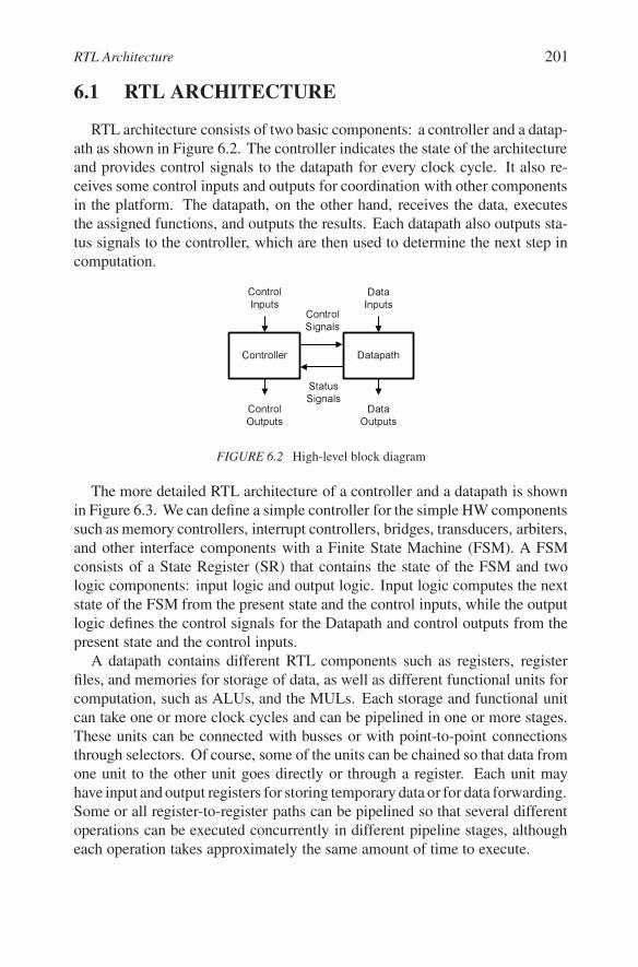
6.1 RTL ARCHITECTURERTL architecture consists of two basic components: a controller and a datap-
ath as shown in Figure 6.2. The controller indicates the state of the architectureand provides control signals to the datapath for every clock cycle. It also re-ceives some control inputs and outputs for coordination with other componentsin the platform. The datapath, on the other hand, receives the data, executesthe assigned functions, and outputs the results. Each datapath also outputs sta-tus signals to the controller, which are then used to determine the next step incomputation.
ControlS i g na ls
Controlle r
ControlO u tp u ts
ControlI np u ts
D a ta p a th
D a taI np u ts
D a taO u tp u ts
S ta tu sS i g na ls
FIGURE 6.2 High-level block diagram
The more detailed RTL architecture of a controller and a datapath is shownin Figure 6.3. We can define a simple controller for the simple HW componentssuch as memory controllers, interrupt controllers, bridges, transducers, arbiters,and other interface components with a Finite State Machine (FSM). A FSMconsists of a State Register (SR) that contains the state of the FSM and twologic components: input logic and output logic. Input logic computes the nextstate of the FSM from the present state and the control inputs, while the outputlogic defines the control signals for the Datapath and control outputs from thepresent state and the control inputs.
A datapath contains different RTL components such as registers, registerfiles, and memories for storage of data, as well as different functional units forcomputation, such as ALUs, and the MULs. Each storage and functional unitcan take one or more clock cycles and can be pipelined in one or more stages.These units can be connected with busses or with point-to-point connectionsthrough selectors. Of course, some of the units can be chained so that data fromone unit to the other unit goes directly or through a register. Each unit mayhave input and output registers for storing temporary data or for data forwarding.Some or all register-to-register paths can be pipelined so that several differentoperations can be executed concurrently in different pipeline stages, althougheach operation takes approximately the same amount of time to execute.

202 Hardware Synthesis
Output L o g i c B1
B2
A L U M e m o r y
R F
M U L
B3F S M C o n t r o l l e r
I n put L o g i c
D a ta pa th
C o n tr o lI n puts
C o n t r o lOutputs
C o n tr o lS i g n a l s
S ta tusS i g n a l s
D a taI n puts
D a taOutputs
SR
FIGURE 6.3 RTL diagram with FSM controller
For larger standard and custom processors and larger special function pro-cessors, the simple FSM controller is usually replaced with a programmablecontroller, as shown in Figure 6.4. In this case, the State Register becomes theProgram Counter (PC); the output logic becomes the Control Memory (CMem)for storing control words, or the Program Memory (PMem) for storing instruc-tions; and the input logic becomes the Address Generator (AG) for generatingthe address of the next control word or the next instruction. The AG maycompute the next address from information supplied by different sources, suchas a datapath address, datapath status signals, an offset from the CW or aninstruction and data supplied by the rest of the platform through control inputs.
This type of programmable controller can be also pipelined by itself or inconjunction with the datapath. Figure 6.4 shows such a pipelined controllertogether with a pipelined datapath. In order to pipeline the controller we mayinsert an Instruction Register (IR) or a Control Word Register (CWR) to storetemporarily instructions or control words. We can also insert a Status Register(SR) to store status signals from the datapath. After insertion of these registers,every instruction or control word as shown in Figure 6.4 needs three cycles tobe generated before applied to the datapath. In the first cycle, AG generatesthe new address for PC from information in registers such as SR or IR or CWRor some other registers in the datapath. In the second cycle a control wordfrom CMem or instruction from PMem is loaded into IR or CWR. Finally, inthe third cycle control word or decoded instruction is applied to the datapath.Furthermore, the number of cycles may increase if CMem or PMem read takesmore than one clock cycle...

Input Models 203
In addition to controller pipelining, datapath can be pipelined at the sametime. For example, the datapath in Figure 6.4 has input and output registerspreceding and following every functional unit. Therefore, it takes one clockcycle to read the data from the RF and transfer it to the ALU input register,one clock cycle to compute the operation in the ALU and store date in theALU output register, and finally one clock cycle to write data back into theRF. Of course, some functional units may be pipelined and take more thanone clock cycle to complete their operation. For example multiplier MUL inFigure 6.4 has two pipelined stages and will take two clock cycles to completemultiplication of two operands in its input registers before the result is storedin the MUL output register. Therefore, data computation from RF to RF inthe datapath of Figure 6.4 may take three (arithmetic and logic operations) orfour (multiplication) clock cycles. With pipelined controller and datapath asshown in FIGURE 6.4, new address generation takes at least four clock cycles:one from the PC to the IR or CWR, the second one to the ALU input registers,the third to the SR or ALU output register, and finally, the fourth one back tothe PC. It may, however, take more than four clock cycles if a new address isdelivered from the local memory which takes longer than one clock cycle toread the address.
Status
A d d r e ss
IR or CWR
C m e mo r
P M e m
A G
SR
PC B1B2
A L U M e m o r y
R F
M U L
B3P r o g r am m ab l e C o n tr o l l e r D ata p ath
O f f se t
C o n t r o lIn p uts
C o n t r o lO utp uts
C o n t r o lSi g n al s
D ataIn p uts
D ataIn p uts
FIGURE 6.4 RTL diagram with programmable controller

204 Hardware Synthesis
6.2 INPUT MODELSInput models for HW component synthesis come in many different forms:
from C-code to RTL to netlists. The C-code input does not contain any designdecisions, while logic netlist, for example, has all the design decisions alreadyimplemented. Many other forms, such as CDFG or FSMD, include some butnot all of the design decisions. We will look at several different input modelsusing the example of the Ones Counter (OC). The OC takes in Data as a stringof 0’s and 1’s, computes the number of 1’s in the Data, and then outputs thisnumber of 1’s after certain amount of time. The OC waits for the Data until theStart signal becomes 1, and then copies the Data and starts counting. It stopswhen all the ones are counted, then outputs the number of ones, sets the Donesignal to 1, and goes to the waiting state, in which it waits for the Start signal togo to 1 again. The OC example can be used to describe different input modelsfor HW component synthesis.
6.2.1 C-CODE SPECIFICATIONProgramming languages such as C were designed to define computation exe-
cuting sequentially on a standard processor. C language describes computationin terms of function calls that return values for a given set of parameters. Sucha description of the OC using C language function call is shown in Listing 6.1.The function OnesCounter sets the variables Ocount to 0, Mask to 1, and leavestemporary variable Temp undefined. After that, it computes the number of onesby storing the least significant bit of the Data into the Temp variable by com-puting Temp = Data & Mask and adding that Temp to the Ocount. After thatit shifts the Data to the right and repeats the computation for the next moresignificant bit. It stops if there are no more 1’s in the Data. Therefore, theOcount computation may take a different number of clock cycles, dependingon the number and position of 1’s in the variable Data.
When the Ones counter is implemented as a function, the input is passed to thefunction via a function argument in line 1. The result of the function is passedback by a return value. The return value is given with the return statement in line09. The function is executed on demand by calling the function and terminatesonce reaching the return statement. Therefore, the call and return are the triggersfor starting and ending the computation. In this way, the function-based C-codedefinition differs from a typical hardware component, which is always runningand waits for control signals to start computing while it communicates throughdata signals with other components.
In order to describe operation of a HW component on RT level more accu-rately, we need to introduce new variables for controller and datapath inputs andoutputs. Furthermore, we need to rewrite the C code in Listing 6.1 to execute

Input Models 205
1 int OnesCounter(int Data){2 int Ocount = 0;3 int Temp, Mask = 1;4 while(Data > 0) {5 Temp = Data & Mask;6 Ocount = Data + Temp;7 Data >>= 1;8 }9 return Ocount;
10 }
LISTING 6.1 Function-based C code
1 while(1) {2 while(Start == 0);3 Done = 0;4 Data = Input;5 Ocount = 0;6 Mask = 1;7 while(Data > 0) {8 Temp = Data & Mask;9 Ocount = Ocount + Temp;
10 Data >>= 1;11 }12 Output = Ocount;13 Done = 1;14 }
LISTING 6.2 RTL-based C code
indefinitely. This is shown in Listing 6.2, which executes forever in the loopshown in line 1, with loop in line 2 waiting for Start to become 1. The C codein Listing 6.2 has several new control and data variables added. Control signalDone is reset to 0 in line 3 and set to 1 in line13 indicating the beginning andending of the component operation. The variables Input and Output representthe data ports to the component while variables Data, Ocount, Mask and Tempare temporary variables for computation inside the component.
In general, designers need to avoid function calls to ensure better understand-ing and easier synthesis of hardware components. As a result of the re-codingshown in Listing 6.2, we now have flat C-code that is suitable for high-levelsynthesis. The code uses Input and Output variables for communication withthe external environment and does not contain any function calls. However, westill can not make distinction between control and data variables in the code inListing 6.2.
6.2.2 CONTROL-DATA FLOW GRAPH SPECIFICATIONA Control-Data Flow Graph (CDFG) [151] represents a C-code with if,
loop, and Basic Block (BB) constructs, where a BB represents a sequence ofprogramming statements without ifs and loops. A CDFG is useful becauseit shows control and data dependences. It allows us to easily follow controldependences between if, loop, and BB constructs in the C-code since each ofthem is represented by a graphical symbol with the control arrows betweenthem. It also allows us to expose concurrency of operations in the C code byrepresenting each BB as a Data-Flow Graph (DFG) in which every operation isrepresented by a node in the graph while arrows between the nodes represent
206 Hardware Synthesis
0
1
>0
0
DoneO u t p u t
I np u t
0Done
0O c ou nt
1M a s kDa t a
&
>>1 +
DoneDa t a
DoneO c ou ntDa t a
S t a r t
Da t a
1
M a s k O c ou nt
FIGURE 6.5 CDFG for Ones counter
input and output variables. Note that the order in which the statements arewritten in the C code imposes unnecessary sequentially on the execution ofthese statements.
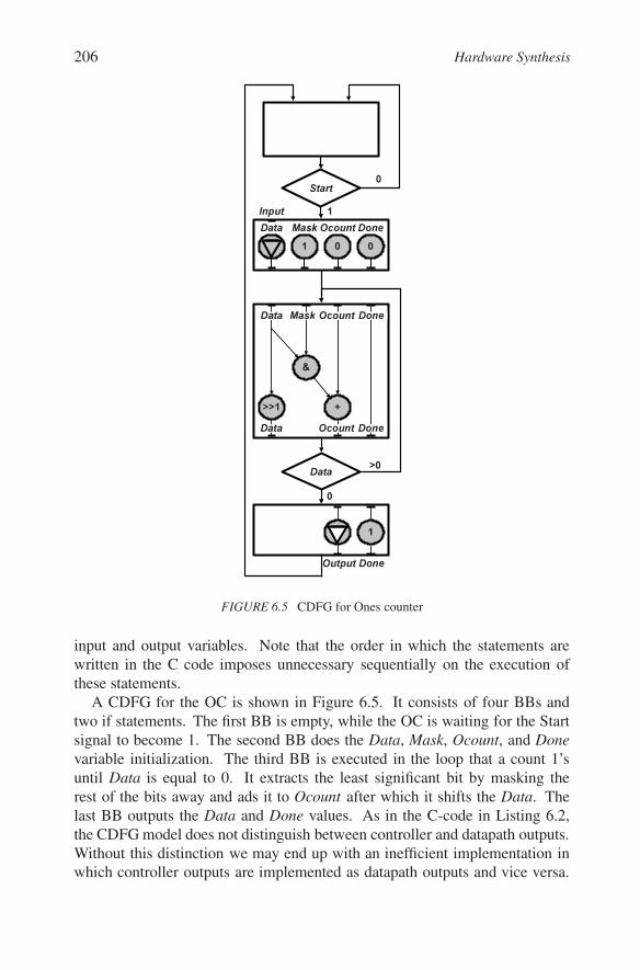
A CDFG for the OC is shown in Figure 6.5. It consists of four BBs andtwo if statements. The first BB is empty, while the OC is waiting for the Startsignal to become 1. The second BB does the Data, Mask, Ocount, and Donevariable initialization. The third BB is executed in the loop that a count 1’suntil Data is equal to 0. It extracts the least significant bit by masking therest of the bits away and ads it to Ocount after which it shifts the Data. Thelast BB outputs the Data and Done values. As in the C-code in Listing 6.2,the CDFG model does not distinguish between controller and datapath outputs.Without this distinction we may end up with an inefficient implementation inwhich controller outputs are implemented as datapath outputs and vice versa.

Input Models 207
However, CDFG can represent a waiting state in which OC waits for Start signalto become 1, similarly to the C code in Listing 6.2 in line 2.
S5
S4
S3
S0
S1
S2
S6
S7
St a r t = 0
D o n e = 0; D a t a = I n p u t
O c o u n t = 0
M a s k = 1
T e m p = D a t a A N D M a s k
O c o u n t = O c o u n t + T e m p
D a t a = D a t a > > 1
D o n e = 1; O u t p u t = O c o u n tD a t a = 0
St a r t = 1
D a t a = 0/
FIGURE 6.6 FSMD specification
6.2.3 FINITE STATE MACHINE WITH DATASPECIFICATION
A Finite State Machine with Data (FSMD) [63, 184] specification is anupgraded version of the well-known Finite State Machine representation pro-viding the same information as the CDFG specification. A FSMD specification,however, can be more specific than the corresponding CDFG specification ifwe assume that each state is executed in one clock cycle. This way a FSMDspecification can provide an accurate estimation of the design performance.The FSMD specification for the OC is shown in Figure 6.6. It has eight statesand requires eight clock cycles to execute. The second BB from the CDFGspecification that contains four initialization operations is executed in states S2,S3, and S4 and therefore requires three clock cycles. Since Done is a controlsignal, it can be executed concurrently with operations on any of the other threevariables. Variables Data, Ocount and Mask, which are presumably in the sameRF, need three states or three clock cycles to execute since their initialization

208 Hardware Synthesis
goes through the same ALU in the implementation. This is also true of thecomputation of the Temp, Ocount, and Data values in states S4, S5, and S6 inthe 1’s counting loop. Therefore, a FSMD specification can offer more accuratetiming information in terms of clock cycles than a CDFG specification. Themain reason for this is that the DFG in each BB in a CDFG is scheduled intostates or clock cycles in the corresponding FSMD.
status
SR O utp ut L o g i c
B1
A L U
S h i f t e r
B3F S M C o n tr o l l e r
I n p ut L o g i c
D ata p ath
D o n e
S ta r t
B2
Selector
O utp o r t
C o n tr o lS i g n al s
I n p o r t
R F
FIGURE 6.7 RTL Specification
6.2.4 RTL SPECIFICATIONRegister-Transfer-Level (RTL) specification provides a Datapath netlist with
all RTL components and their connections. It also includes two tables forsynthesis of input logic and output logic components in the FSM Controller.We can automatically obtain Boolean equations for synthesis of input logic fromthe input logic table after we define some state encoding for the states in thetable. Similarly, we can automatically obtain Boolean equations for the outputlogic from the output logic table which defines variable bindings to storageelements and operations to functional units.
For example, RTL specification for the OC is given in Figure 6.7, and inTable 6.1 and Table 6.2. In the ones counter architecture, shown in Figure 6.7,variables Data, Mask, Ocount, and Temp are in the registers RF[0], RF[1],RF[2], and RF[3] of the two port register file RF. They communicate throughbuses B1 and B2 with two chained functional units, ALU and Shifter. Shifteralso provides the status signal Data = 0 to the input logic in the FSM Controller.The input logic table in Table 6.1 supplies logic equations for the next state and

Input Models 209
the control output signal Done. We can see that Done = 1 when the SR is in stateS7. Similarly, we can derive Boolean equations for the output logic from theoutput logic table shown in Table 6.2 once control encoding for every storageand functional unit is taken into account.
TABLE 6.1 Input logic table
S0S7S4S6S5S4S3S2S1S0
StateN ex t
1XXS701XS6
XXXXXX10
Star tI n p u ts : O u tp u t:P r es en t
0XS500S6
0XS40XS30XS20XS1XXS0XXS0
D o n eD ata = 0State
S0S7S4S6S5S4S3S2S1S0
StateN ex t
1XXS701XS6
XXXXXX10
Star tI n p u ts : O u tp u t:P r es en t
0XS500S6
0XS40XS30XS20XS1XXS0XXS0
D o n eD ata = 0State
TABLE 6.2 Output logic table
RF[0] = DataRF[1 ] = M as kRF[2 ] = O c o u n tRF[3 ] = T e m p
RF[2]
RF[0 ]
RF[2]
RF[0 ]RF[2]RF[2]
X
X
RF Read P o r t A
X
p a s s
a d d
A N Di n c r e m e n ts u b t r a c t
X
X
A L U
X
X
RF[3 ]
RF[1 ]X
RF[2]
X
X
RF Read P o r t B
X
B 3
B 3
B 3B 3B 3
I n p o r t
X
RF s el ec t o r
X
s h i f t r i g h t
p a s s
p a s sp a s sp a s s
X
X
S h i f t er
d i s a b l e
RF[0 ]
RF[2]
RF[3 ]RF[1 ]RF[2]
RF[0 ]
X
RF W r i t e
e n a b l eS 7
ZS 6
ZS 5
ZS 4ZS 3ZS 2
ZS 1
ZS 0
O u t p o r tS t at e
RF[2]
RF[0 ]
RF[2]
RF[0 ]RF[2]RF[2]
X
X
RF Read P o r t A
X
p a s s
a d d
A N Di n c r e m e n ts u b t r a c t
X
X
A L U
X
X
RF[3 ]
RF[1 ]X
RF[2]
X
X
RF Read P o r t B
X
B 3
B 3
B 3B 3B 3
I n p o r t
X
RF s el ec t o r
X
s h i f t r i g h t
p a s s
p a s sp a s sp a s s
X
X
S h i f t er
d i s a b l e
RF[0 ]
RF[2]
RF[3 ]RF[1 ]RF[2]
RF[0 ]
X
RF W r i t e
e n a b l eS 7
ZS 6
ZS 5
ZS 4ZS 3ZS 2
ZS 1
ZS 0
O u t p o r tS t at e
6.2.5 HDL SPECIFICATIONRTL specification in VHDL/Verilog provides a FSMD description from
which we can derive a datapath netlist with all RTL components and theirconnections, as well as a FSM description for logic synthesis of the input logicand output logic.
210 Hardware Synthesis
1 // ...2 always@(posedge clk)3 begin : output logic4 case (state)5 // ...6 S4: begin7 B1 = RF[0];8 B2 = RF[1];9 B3 = alu(B1, B2,l and);
10 RF[3] = B3;11 next state = S5;12 end13 // ...14 S7: begin15 bus 32 0 = RF[2];16 Outport <= B3;17 Done <= 1;18 next state = S0;19 end20 endcase21 end22 endmoduleLISTING 6.3 RTL description in HDL (excerpt)
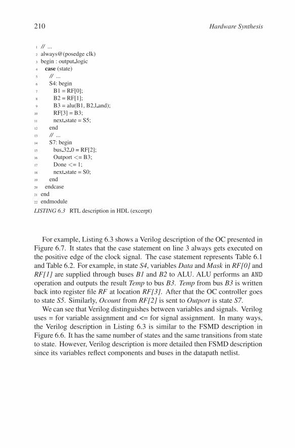
For example, Listing 6.3 shows a Verilog description of the OC presented inFigure 6.7. It states that the case statement on line 3 always gets executed onthe positive edge of the clock signal. The case statement represents Table 6.1and Table 6.2. For example, in state S4, variables Data and Mask in RF[0] andRF[1] are supplied through buses B1 and B2 to ALU. ALU performs an AND
operation and outputs the result Temp to bus B3. Temp from bus B3 is writtenback into register file RF at location RF[3]. After that the OC controller goesto state S5. Similarly, Ocount from RF[2] is sent to Outport is state S7.
We can see that Verilog distinguishes between variables and signals. Veriloguses = for variable assignment and <= for signal assignment. In many ways,the Verilog description in Listing 6.3 is similar to the FSMD description inFigure 6.6. It has the same number of states and the same transitions from stateto state. However, Verilog description is more detailed then FSMD descriptionsince its variables reflect components and buses in the datapath netlist.

Estimation and Optimization 211
6.3 ESTIMATION AND OPTIMIZATIONHLS starts with the selection of some initial RTL components such as storage
components, functional units, and buses. The datapath then executes variableassignments in every clock cycle, a process by which selected variables willbe assigned new values through arithmetic, logic, and shift operations that areperformed by functional units. To execute each variable assignment statement,then, the datapath must take data from a storage component that stores the vari-ables in the right-hand side of the assignment, pass this data to the functionalunits that compute the new value, and then pass it back to the storage compo-nent, which stores the variables on the left-hand side of the equation. Giventhis process, it follows that we can approach datapath creation by selectingthe storage components, the functional units, and the buses that connect thesecomponents.
By focusing on the storage components, for example, we note that the vari-ables in the datapath must be stored in registers, register files, and memories.However, since not all variables are alive at the same time, it is possible forcertain variables to share the same register or the same location in a register fileor a memory. In other words, we can merge the datapath variables in a waythat reduces the number of storage locations in the datapath. Furthermore, evenif certain variables are alive at the same time, they may not be accessed at thesame time, which means that we could combine them into a register file or ascratch-pad memory so that they can share the same register file or memoryports. In this manner, by combining storage locations we minimize the num-ber of storage ports in the datapath and thus reduce the number of connectionsneeded.
We can reduce the number of functional units in the datapath in a similarway. As mentioned above, in each state, selected variables are to be assignednew values through various arithmetic, logic, or shift operations, each of whichcan be performed by a separate functional unit. However, since most of theseoperations are executed in different clock cycles, they could share the samefunctional unit. In other words, we can reduce the number of units in thedatapath by combining different operations into groups, allowing each groupof operations to be executed in a single functional unit.
The third basic technique for optimization focuses on the datapath connec-tivity. As mentioned above, the execution of an assignment statement requiresthat data pass from one storage component to the functional unit that computesthe new value and then back to another storage component. The data, in otherwords, is passed through connections between storage and functional units.However, since different connections will be used in different states, we cangroup connections into buses, which enable us to reduce the number of wiresin the datapath.

212 Hardware Synthesis
Controller ControlS i g na ls
S ta rt
D one
D a ta p a th
I n 1
Ou t
I n 2
(a) SRA block diagram
S0a = I n 1b = I n 2
0
1
Star t
S1
S2
S3
S4
S5
S6
S7
t1 = |a|t2 = |b|
t5 = x – t3
x = m ax ( t1 , t2 )y = m i n ( t1 , t2 )
t3 = x > > 3t4 = y > > 1
t6 = t4 + t5
t7 = m ax ( t6 , x )
D o n e = 1O u t = t7
(b) FSMD model of SRA
FIGURE 6.8 Square-root algorithm (SRA)
The components can be selected by assuming that one operation is executedevery clock cycle or that all possible operations not dependent on each otherare executed in the same clock cycle. In the first case, we have a cost-drivendesign, while in the latter, we have a performance-driven design.
These three basic allocation techniques can be demonstrated on a small ex-ample dedicated to computing of the Square-Root Approximation (SRA) of twosigned integers, a and b, by the following formula:√
a2 + b2 ≈ max((0.875x + 0.5y), x)where x = max(|a|, |b|) and y = min(|a|, |b|).According to the FSMD model in Figure 6.8(a) this component has two input
ports, In1, and In2, which are used to read integers a and b, and one output portOut. As you can see in the FSMD model in Figure 6.8(b), the componentreads the input ports and starts the computation whenever the input control

Estimation and Optimization 213
signal Start becomes equal to 1. In state S1, it computes the absolute valuesof variables a and b, and in S2, it assigns the maximum of these two values tox and the minimum to y. In state S3 it shifts x three positions to the right toobtain 0.125x and shifts y one position to the right to obtain 0.5y. The SRAcomponent calculates 0.875x by subtracting 0.125x from x in state S4. In stateS5 it adds 0.875x and 0.5y, while in state S7 it computes the maximum of xand the expression 0.875x + 0.5y. In state S7, the SRA component producesthe result and makes it available through the Out port for one clock cycle. Atthe same time, it sets the control signal Done to 1, in order to signal to theenvironment that the data that has appeared at the Out port is a valid result.
To determine resource requirements from this FSMD model, we would needto generate the variable and operation usage tables shown in Table 6.3 andTable 6.4. In the variable-usage table, each row represents one variable foundin the FSMD model and each column represents one state. For each variable,then, we would enter an x in the columns that correspond to the states in whichthe variable is alive. A variable is considered alive in the first state that followsthe rising edge of the clock signal which assigns its new value and also in allstates inclusively between the first and final states in which this new value isused for the last time. In Table 6.3, for example, variables a and b are assignedtheir values at the rising edge of the clock signal indicating the beginning ofstates, but they are not used in any other states.
TABLE 6.3 Variable usage
1233222No. of live var iables
Xt 7Xt 6
Xt 5
XX
S 1
XX
S 3
XX
S 2
X
X
S 5
XX
X
S 4
X
S 6
t 4t 3yxt 2t 1ba
S 7
1233222No. of live var iables
Xt 7Xt 6
Xt 5
XX
S 1
XX
S 3
XX
S 2
X
X
S 5
XX
X
S 4
X
S 6
t 4t 3yxt 2t 1ba
S 7
Therefore, variables a and b are alive only in state S1. By contrast, variablex is assigned its new value at the beginning of state S3, but the value of x isalso used in states S4 and S6, indicating that the variable x is alive in states S3,S4, S5, and S6. On the basis of this table, then, we can see which variables arealive in which states.

214 Hardware Synthesis
TABLE 6.4 Operation usage
S7
111212N o . o fo p e r a t i o n s
2
S1
2
S3
11
S2
1
S5
1
S4
1
S6
1+1-2> >1m a x1m i n2a b s
M a x . n o . o f u n i t s
S7
111212N o . o fo p e r a t i o n s
2
S1
2
S3
11
S2
1
S5
1
S4
1
S6
1+1-2> >1m a x1m i n2a b s
M a x . n o . o f u n i t s
More importantly, however, Table 6.3 also shows the maximum number ofvariables alive in a single state. That is, it shows us that in states S4 and S5 thereare three live variables. We would therefore conclude that we will need at leastthree registers in the datapath of this SRA design. Because of this, we may beable to combine variables from Table 6.3 into three groups so that each groupthat is to be stored in one of the registers contains only variables that are notalive at the same time. On the basis of this example, then, you can see that oneof the major tasks in RTL synthesis consists of merging or grouping variablesand assigning the groups to registers or memory locations in a way that willminimize the number of storage components or some other design metric, suchas performance, power, or testability. Since each group of variables shares aregister or memory location, this task is also frequently called register/memorysharing.
In a similar fashion, we might determine the minimum number of unitsneeded to execute all the operations in the design. For this purpose we woulduse Table 6.4, in which the rows represent the different operator types foundin the FSMD model and the columns represent the states, as before. From thistable we can conclude that we need two units that can compute absolute value(indicated by | | in the FSMD model) and shift data (indicated by ») and one unitthat can perform max, min, +, and - operations. Given these requirements, thestraightforward approach to designing the datapath for the SRA is to allocatetwo units for computation of absolute value, two shifters, and one unit each forthe computation of maximums and minimums, one adder, and one subtractor.The problem with this straightforward implementation, however, is that we donot necessarily need one functional unit per operation. Since no state uses all ofthese operations simultaneously, the implementation of one unit per operationwill have functional units idling most of the time. In fact, we do not needmore than two operations in any one state, so it is more efficient to constructfunctional units that can perform more than one operation, as this allows asubstantial hardware saving.

Estimation and Optimization 215
For example, in the SRA description, addition and subtraction are neverperformed at the same time, which means that we can merge these operationsinto one functional unit called an adder/subtractor. In this case we gain oneadder and a complementer at the expense of an additional EX-OR logic. On theother hand, merging the 1-bit shifter and the 3-bit shifter does not save hardwarebut requires an additional selector. On the basis of these examples, you can seehow we perform the second major task in RTL synthesis, which consists ofmerging or grouping operators and designing a functional unit for each group,thereby minimizing a given design metric such as area, the number of gates ortransistors, or the number of functional units in the datapath. This task is alsocalled functional-unit sharing.
TABLE 6.5 SRA connectivity
IO
t5
O
I
t6
O
t7
I
O
t3
I
O
t4I
a
II
O
t1
I
b
I
IIO
x
IIO
t2
I
O
y
+-
> > 1> > 3m axm i nabs 2abs 1
IO
t5
O
I
t6
O
t7
I
O
t3
I
O
t4I
a
II
O
t1
I
b
I
IIO
x
IIO
t2
I
O
y
+-
> > 1> > 3m axm i nabs 2abs 1
If our primary goal is to minimize wiring, we should also consider mergingconnections into buses, since each single connection between any two unitswould be used in very few states and would mostly remain idle. As an example,let us consider the connections in an SRA datapath that uses one register pervariable and single-operation functional units. The connections for such adatapath are given in the connectivity table shown in Table 6.5, in which eachrow corresponds to one functional unit and each column represents one register.To complete the table, we enter the letter I for every connection between aregister and the input of a functional unit, and for every connection betweenthe output of the functional unit and a register, we enter the letter O. As youcan see in Table 6.5, such an SRA requires 14 input connections and 9 outputconnections, for a total of 23 connections. Of these 23 connections, however,very few are needed in any one state. From the FSMD model, in fact, weknow that the maximum number of connections is used in state S2 is four inputconnections, which link the registers storing the variables t1 and t2 to the minand max units as well as two output connections, linking min and max unitsto the registers that store the variables x and y. In other words, the maximumnumber of connections needed concurrently is six.

216 Hardware Synthesis
From this example, you can see that the third major task in RTL synthesisconsists of merging or grouping connections and assigning one bus to eachgroup so as to minimize the connection cost. Note that this connection costincludes the cost of bus drivers, which are required for every connection of aunit to a bus, and the cost of input selectors, which are required whenever twoor more buses are connected to the same input of a storage or functional unit.This task is also frequently called bus sharing.
6.4 REGISTER SHARINGAs we mentioned earlier, one of the major tasks in datapath optimization
involves grouping variables so that they share a common register or memorylocation. The advantage of such grouping lies in the fact that it reduces thenumber and size of storage components, which in turn reduces the silicon areaand therefore the cost of fabrication. Since a register can be shared only bythose variables with non-overlapping lifetimes, this technique requires us todetermine the lifetimes of each variable.
The lifetime of a variable is defined as the set of states in which that variableis alive, which includes the state following the state in which it is assigned anew value (write state), every state in which it is used on the right-hand side ofan assignment statement (read state), and all the states on each path betweenthe write state and a read state. Note also that each variable may have multipleassignments and that each assigned value may be used several times. Oncewe determine the lifetime of each variable, we can group variables that havenon-overlapping lifetimes and assign each group to a single register.
When we group variables, one of the common goals is to try to have as fewregisters as possible, which means that we would try to partition variables intothe smallest number of groups while ensuring that every variable belongs toone of these groups. This goal can be accomplished by a simple algorithm suchas left-edge algorithm, which tries to pack as many variables as possible intoeach register. Left-edge algorithm is simple and fast, but it does not take intoaccount the overall datapath structure.
As we demonstrated in the previous section for the SRA example, we cannotreduce the number of registers in the datapath to fewer than three. However,since there are many possible datapath designs with three registers, we wouldlike to select one that minimizes a second design metric, such as connectivitycost. For example, the cost of connecting I/O ports, registers, and functionalunits can be measured in the number of selector inputs, assuming that the costper selector input is constant.
To develop an algorithm that will minimize the number of registers as wellas connectivity cost, we give priority to the combining of certain variables.

Register Sharing 217
x = a + b
y = c + dS j
S i
(a) PartialFSMD
a
S e l e ct o r S e l e ct o r
S e l e ct o r S e l e ct o r
c b d
x y
+
(b) Datapath without registersharing
Selector Selector
a , c b , d
x , y
+
Selector
(c) Datapath with registersharing
FIGURE 6.9 Gain in register sharing
Priority is given to two variables that are used as the left or right operands forthe same operator type and to variables whose value is generated by the sameoperator type, since merging such variables can potentially save one selectorinput. This concept is demonstrated in Figure 6.9(a) for two additions (x = a +b and y = c + d) performed in different states on different operands and assignedto different variables. If we assume that both additions may be executed in thesame functional unit, merging operands and results may result in the saving ofselector inputs. For example, if we assign each variable to a separate register,we may obtain the design shown in Figure 6.9(b), which requires 10 selectorinputs. However, if we merge variable a with c, b with d, and x with y, thenassign each pair to the same register, we reduce number of selector inputs bythree, as shown in Figure 6.9(c).
In general, for any n variables that are used as a source or a destination to thesame operator or functional unit, there is a potential saving of n -1 selector inputswhen these n variables share the same register. To consider this potential savingduring variable merging, we present a partitioning algorithm, which partitions avariable compatibility graph. Such a compatibility graph consists of nodes andedges in which each node represents a variable and each edge between two nodesrepresents compatibility or incompatibility in merging variables represented bythese two nodes. There are two types of edges in the graph: an incompatibilityedge (represented by a dashed line) between two nodes indicates variableswith overlapping lifetimes, while a priority edge between two nodes indicatesvariables with non-overlapping lifetimes that serve as the source or destinationto the same functional units. Each priority edge has a priority weight indicatingthe number of selector inputs that can be saved. The priority weight has theform s/d, where s is equal to the number of different functional units that use
218 Hardware Synthesis
both nodes as left or right operands, and d is equal to the number of differentfunctional units that generate results for both nodes.
Stop
n o y e s
C r e a te c om pa ti b i l i ty g r a ph
M e r g e h i g h e s t pr i or i ty n od e s
U pg r a d e c om pa ti b i l i ty g r a ph
A l l n od e s i n c om pa ti b l e
Sta r t
FIGURE 6.10 General partitioning algorithm
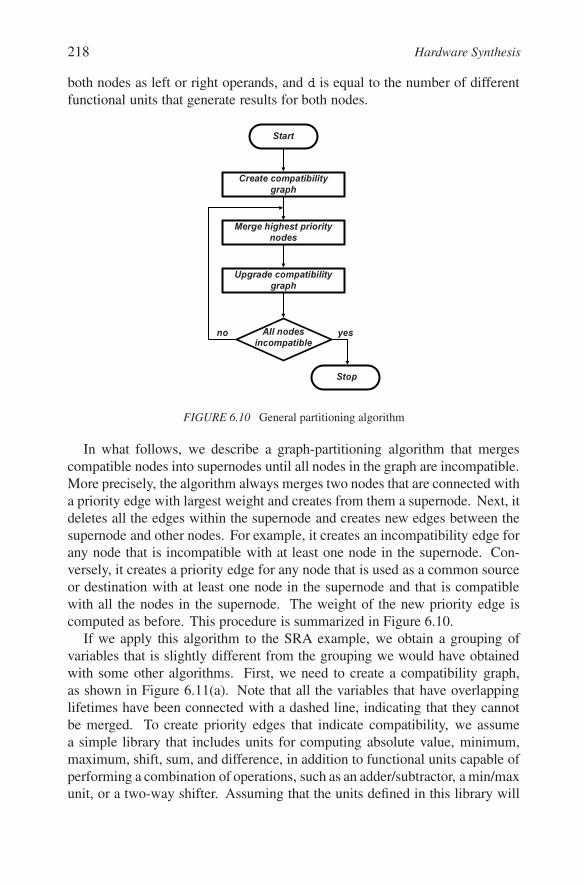
In what follows, we describe a graph-partitioning algorithm that mergescompatible nodes into supernodes until all nodes in the graph are incompatible.More precisely, the algorithm always merges two nodes that are connected witha priority edge with largest weight and creates from them a supernode. Next, itdeletes all the edges within the supernode and creates new edges between thesupernode and other nodes. For example, it creates an incompatibility edge forany node that is incompatible with at least one node in the supernode. Con-versely, it creates a priority edge for any node that is used as a common sourceor destination with at least one node in the supernode and that is compatiblewith all the nodes in the supernode. The weight of the new priority edge iscomputed as before. This procedure is summarized in Figure 6.10.
If we apply this algorithm to the SRA example, we obtain a grouping ofvariables that is slightly different from the grouping we would have obtainedwith some other algorithms. First, we need to create a compatibility graph,as shown in Figure 6.11(a). Note that all the variables that have overlappinglifetimes have been connected with a dashed line, indicating that they cannotbe merged. To create priority edges that indicate compatibility, we assumea simple library that includes units for computing absolute value, minimum,maximum, shift, sum, and difference, in addition to functional units capable ofperforming a combination of operations, such as an adder/subtractor, a min/maxunit, or a two-way shifter. Assuming that the units defined in this library will

Register Sharing 219
t1
t2
t3
t4
t5 t6
t7x
a y
b
��� � � � �
1/0
1/0
0/1
1/0 0/1
0/1
(a) Initial compability graph
a
b
t1
t2
y
x
t4
t3 t5 t6t7
1/0� � �
1/0
1/0
1/0
0/1
(b) Compatibility graph after merging t3,t5, and t6
a
b t1t2
y
x
t4
t3 t5 t6
t71/0
(c) Compatibility graph after mergingt1, x, and t7
a
b t1
t2 y
x
t4
t3 t5 t6
t7
(d) Compatibility graph after merging t2and y
a
b
t1
t2 y
x
t4
t3 t5 t6
t7
(e) Final compatibility graph
R1 = [ a, t1, x, t7 ]R2 = [ b, t2, y, t3, t5, t6 ]R3 = [ t4 ]
(f) Final registerassignments
FIGURE 6.11 Variable merging for SRA example
be used in the final design, we find that there are priority edges between thevariables t1, t2, and x, and t1, t2, and t6. Since they are all inputs of the samemax unit; there are priority edges between the variables x, y, and t7 becausethey are possible destinations of a min/max unit. There are also priority edgesbetween t3 and t5, and t5 and t6 because they all are possible inputs and outputsof an adder/subtractor.
After creating this compatibility graph, we can start merging variables andcreating supernodes. In this case, all the priority edges have the same weight,so we first select those nodes whose merging will not remove any priority edgesfrom the compatibility graph. In other words, we merge the variables t3, t5,and t6 for a possible gain of two selector inputs, thereby creating the supernode[t3, t5, t6], as shown in Figure 6.11(b). Next, we select the node that has amaximum number of priority edges, namely x, and merge it with t7 and thent1 as shown in Figure 6.11(c). Note that by merging x, t7, and t1, we have
220 Hardware Synthesis
removed three priority edges from the compatibility graph, one from betweeny and t7, one from between t2 and x, and a third from between t1 and t6. At thispoint we can merge t2 and then y with the supernode [t3, t5, t6], as shown inFigure 6.11(d). Finally, we can randomly assign the variable a to the supernode[t1, x, t7] and b to the supernode [t2, y, t3, t5, t6] to further reduce the number ofregisters needed, so that the supernode [a, t1, x, t7] can be assigned to registerR1, while supernode [b, t2, y, t3, t5, t6] is assigned to register R2, and [t4] toregister R3.
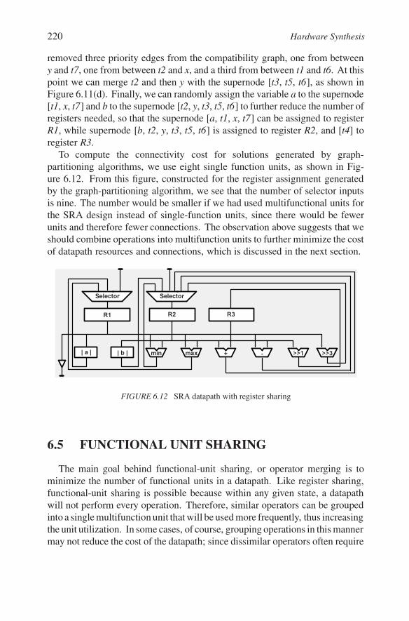
To compute the connectivity cost for solutions generated by graph-partitioning algorithms, we use eight single function units, as shown in Fig-ure 6.12. From this figure, constructed for the register assignment generatedby the graph-partitioning algorithm, we see that the number of selector inputsis nine. The number would be smaller if we had used multifunctional units forthe SRA design instead of single-function units, since there would be fewerunits and therefore fewer connections. The observation above suggests that weshould combine operations into multifunction units to further minimize the costof datapath resources and connections, which is discussed in the next section.
Selector Selector
R1 R2 R3
| a | | b | m i n m a x + - > > 1 > > 3
FIGURE 6.12 SRA datapath with register sharing
6.5 FUNCTIONAL UNIT SHARINGThe main goal behind functional-unit sharing, or operator merging is to
minimize the number of functional units in a datapath. Like register sharing,functional-unit sharing is possible because within any given state, a datapathwill not perform every operation. Therefore, similar operators can be groupedinto a single multifunction unit that will be used more frequently, thus increasingthe unit utilization. In some cases, of course, grouping operations in this mannermay not reduce the cost of the datapath; since dissimilar operators often require

Functional Unit Sharing 221
structurally different designs, grouping them can sometimes result in no gainor even in a higher cost.
x = a + b
y = c + dS j
S i
(a) PartialFSMD
a b
x
+
c d
y
-
(b) Non-shared design
a
S e l e ct o r S e l e ct o r
c b d
x y
+/-
(c) Shared design
FIGURE 6.13 Gain in functional unit sharing
In many cases, however, operator merging can yield cost reductions that arenot negligible, as demonstrated in Figure 6.5. In this example, we have assumedthat the datapath will perform two different operations, addition and subtrac-tion, on different operands in different states, as indicated in Figure 6.13(a). Ifwe implemented a partial FSMD in Figure 6.13(a) using single-function units,we would get the design shown in Figure 6.13(b), in which the datapath re-quires both an adder and a subtractor. We could, however, obtain the samefunctionality by using only one adder/subtractor and two selectors, as shownin Figure 6.13(c). Obviously, the second design would be preferable when thecost of an adder/subtractor and two selectors is less than the cost of a separateadder and subtractor. It is in cases like this that functional-unit sharing would beadvantageous. Thus we would like to develop an algorithm that will combineoperators into functional units in such a way that the total cost of all multifunc-tion units and necessary selectors is minimal. For this purpose, we can use thegraph-partitioning algorithm presented in the previous section. We demonstrateoperator merging with this algorithm on the SRA example. For this example,we assume the availability of a complex component library that includes sev-eral multifunction units that can each compute three of more of the followingoperations: absolute value, minimum, maximum, sum, and difference.
To merge the operators called for in the FSMD model, we must first constructa compatibility graph that indicates which operators can be combined. Eachnode in the compatibility graph represents one operator type from the FSMDmodel, although each graph may have several nodes for each operator type. As arule, the number of nodes will be equal to the maximum number of occurrencesof a particular operator type in any single state. To indicate the compatibility ofthe various operators, we need to connect the nodes in the graph with priority
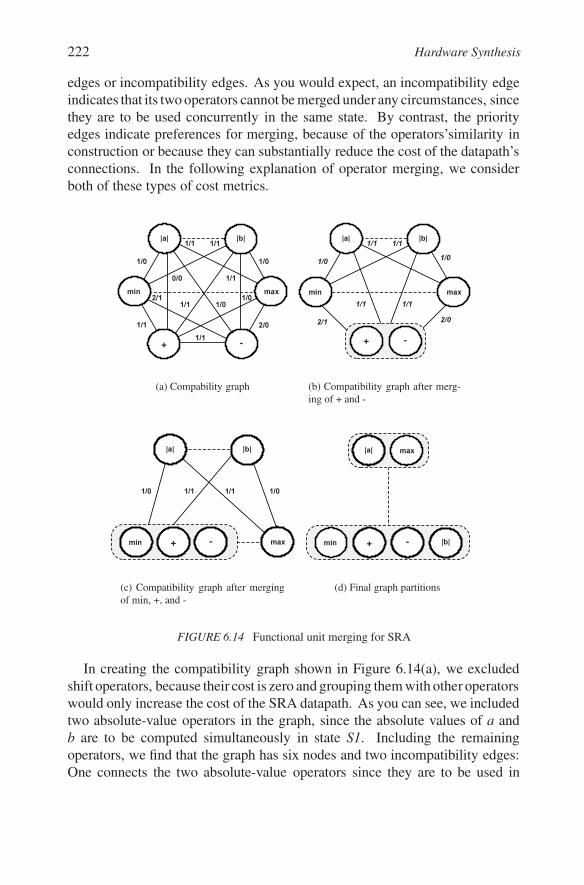
222 Hardware Synthesis
edges or incompatibility edges. As you would expect, an incompatibility edgeindicates that its two operators cannot be merged under any circumstances, sincethey are to be used concurrently in the same state. By contrast, the priorityedges indicate preferences for merging, because of the operators’similarity inconstruction or because they can substantially reduce the cost of the datapath’sconnections. In the following explanation of operator merging, we considerboth of these types of cost metrics.
1/0
|a| |b|
m i n m ax
+ -
1/0
1/0 1/0
1/1 1/1
0/0 1/1
1/1
1/11/1 2/0
2/1
(a) Compability graph
|a| |b|
m i n m ax
+ -
1/0
1/1 1/1
1/1
2/1 2/0
1/1
1/0
(b) Compatibility graph after merg-ing of + and -
1/0
|a| |b|
m i n m ax+ -
1/01/11/1
(c) Compatibility graph after mergingof min, +, and -
|a| m ax
|b|m i n + -
(d) Final graph partitions
FIGURE 6.14 Functional unit merging for SRA
In creating the compatibility graph shown in Figure 6.14(a), we excludedshift operators, because their cost is zero and grouping them with other operatorswould only increase the cost of the SRA datapath. As you can see, we includedtwo absolute-value operators in the graph, since the absolute values of a andb are to be computed simultaneously in state S1. Including the remainingoperators, we find that the graph has six nodes and two incompatibility edges:One connects the two absolute-value operators since they are to be used in
Functional Unit Sharing 223
the same state, while the second edge connects the maximum and minimumoperators since they are incompatible for the same reason.
If we had used single-function units, then implementing the SRA datapathwould require two absolute-value units and one unit each for maximum, min-imum, addition, and subtraction. Intuitively, the total cost of all these unitswould be too high. Therefore, we need to use complex functional units that cando several different arithmetic operations. By merging operators in the compat-ibility graph, we can reduce the datapath cost in several different ways. Lookinginto compatibility graph we see two alternatives. One is to merge |a| and minoperators in one group, and |b|, max, +, and - into another multi-function unit.The other alternative is to merge |a|, min, and + in one, and |b|, max, and -operators into another functional unit. Note that either one of these alternativeswould cost much less than the original implementation using single-functionunits. In general, the designs generated by operator merging have much lowerfunctional-unit costs, which means that as a whole, these designs are morecost-efficient.
However, it is also possible to reduce the datapath cost further by minimizingconnectivity cost while merging operators. To achieve this, we must use thepriority edges in the compatibility graph, as we did in the case of variablemerging. Again, the weight of these priority edges is based on the number ofcommon sources and common destinations.
Returning to the compatibility graph shown in Figure 6.14(a), we can nowadd priority edges and redesign the SRA datapath so as to reduce the number ofselector inputs while merging operators. In Figure 6.14(a), for example, we havelabeled each priority edge with a weight s/d, in which s indicates the number ofcommon sources and d indicates the number of common destinations. As youcan see, the edge between the + and - operators is labeled 1/1, since two sourcevariables (right operands), t3 and t5, and two destination variables, t5 and t6,share register R2. Similarly, the edge between the min and - operators is labeled2/1, since min and - have two common sources and one common destination,that is, the left operands, t1 and x, share register R1, the right operands, t2 andt3, share register R2, and the results, y and t5, share register R2.
At this point we can use the graph-partitioning algorithm presented in Fig-ure 6.10 to group these operators into the appropriate functional units. Accord-ing to this algorithm, we first try to group those operators that have a similardesign structure, such as addition and subtraction, min and max, and left shiftand right shift. In general, grouping similar operators in this manner will pro-duce the largest cost reduction. In the case of the SRA algorithm, for example,we could group the + and - operators into a single supernode and then redrawthe compatibility graph as shown in Figure 6.14(b). Next, we add the minoperator to this supernode, since it has the largest number of common sources(two) and destinations (one) of all the nodes in the graph. This next version

224 Hardware Synthesis
of the compatibility graph is shown in Figure 6.14(c). Finally, we add to thissupernode the absolute-value operator for variable b, for the same reason, andthen merge the max operator with the absolute-value operator for variable a. Atthis stage we have arrived at the graph partition shown in Figure 6.14(d), whichcannot be reduced further.
Selector Selector
R1 R2 R3
a b s /m a x> > 1Selector
a b s /m i n /+ /-
> > 3
FIGURE 6.15 SRA design after register and unit merging
As you can see from this partitioned graph, we should be able to constructa datapath for the SRA algorithm by using three registers and four functionalunits. The final assignment of the variables and operators to their registers andfunctional units as generated in Figure 6.10 and Figure 6.13, produces the data-path schematic as shown in Figure 6.15. Note that this datapath design requiresonly seven selector inputs, in comparison with the nine or more selector inputsrequired by the other design solutions, which did not take merging prioritiesinto account.
6.6 CONNECTION SHARINGIn previous sections we have seen how to merge variables and operators and
assign them to registers and functional units. After assigning them, however,we still need to connect these registers and functional units into a datapath,wiring each register output to the input of a functional unit and each functional-unit output to the input of a register. The outputs of registers and functionalunits are called connection sources, and their inputs are called connection des-tinations. Since several connections can have the same destination at differenttimes, a datapath often includes selectors that are designed to provide the properconnection at the proper time.
Since the connections of a datapath usually occupy a substantial siliconarea, we generally try to reduce the number of connections by merging severalconnections into a bus, which occupies less area. As was the case when we were

Connection Sharing 225
merging variables and operators, we do this by grouping all those connectionsthat are not being used at the same time and assigning each of these groupsto a bus. Each connection source in the group is connected to a bus througha tri-state bus driver which drives the bus in those states in which that sourcesends data to its destination; otherwise, the source is disconnected from the bus.
The technique for merging connections is similar to those techniques we usedfor merging variables and operators. First, we create a connection usage table,which indicates the states in which each connection is to be used. Second, wecreate from this usage table a compatibility graph in which each connection isrepresented by a node and any two nodes can be connected by a priority edge oran incompatibility edge. As the name implies, two nodes are connected by anincompatibility edge whenever their corresponding connections do not originatefrom the same source but are to be used at the same time. Conversely, the nodesare connected by priority edges whenever their corresponding connections havea common source or a common destination. Once we have constructed thiscompatibility graph, we use a graph-partitioning algorithm to group connectionsin a way that will maximize the number of priority edges included in all groups.
Selector Selector
R1 R2 R3
a b s /m a x> > 1 > > 3Selector
a b s /m i n /+ /-
A B C D E F G H
IJ
K L
M NIn 1 In 2
O u t
FIGURE 6.16 SRA Datapath with labeled connections
In Figure 6.16, we demonstrate connection merging for the SRA datapathpresented in Figure 6.15. Every point-to-point connection is indicated with aletter. From Figure 6.16 and the FSMD model, we can create a connectionusage, shown in Table 6.6. In this table, an X has been used to designate thestate in which each connection is to be used. Note that this table containsboth input connections, which link register outputs to functional unit inputs,and output connections, which link functional unit outputs to the appropriateregister inputs. To simplify the partitioning task, it is useful to separate thesetwo types of connections and partition each type separately. By separating thesetwo types of connections, we create separate input and output buses, which willsimplify the datapath architecture.
226 Hardware Synthesis
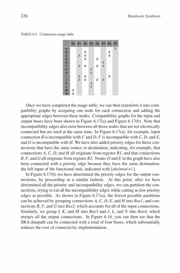
TABLE 6.6 Connection usage table
XNXM
XLXK
XXXXJXXXI
XX
S 6XS 7S 0
X
XXX
S 2
X
X
S 1
X
X
S 4
XX
S 3
XX
S 5
HGFEDCBA
XNXM
XLXK
XXXXJXXXI
XX
S 6XS 7S 0
X
XXX
S 2
X
X
S 1
X
X
S 4
XX
S 3
XX
S 5
HGFEDCBA
Once we have completed the usage table, we can then transform it into com-patibility graphs by assigning one node for each connection and adding theappropriate edges between these nodes. Compatibility graphs for the input andoutput buses have been shown in Figure 6.17(a) and Figure 6.17(b). Note thatincompatibility edges also exist between all those nodes that are not electricallyconnected but are used at the same time. In Figure 6.17(a), for example, inputconnection B is incompatible with C and D, F is incompatible with C, D, and E,and G is incompatible with H. We have also added priority edges for those con-nections that have the same source or destination, indicating, for example, thatconnections A, C, D, and H all originate from register R1, and that connectionsB, F, and G all originate from register R2. Nodes D and E in the graph have alsobeen connected with a priority edge because they have the same destination,the left input of the functional unit, indicated with [abs/min/+/-].
In Figure 6.17(b) we have determined the priority edges for the output con-nections, by proceeding in a similar fashion. At this point, after we havedetermined all the priority and incompatibility edges, we can partition the con-nections, trying to cut all the incompatibility edges while cutting as few priorityedges as possible. As shown in Figure 6.17(a), the fewest possible partitionscan be achieved by grouping connections A, C, D, E, and H into Bus1, and con-nections B, F, and G into Bus2, which accounts for all of the input connections.Similarly, we group I, K, and M into Bus3 and J, L, and N into Bus4, whichmerges all the output connections. In Figure 6.18, you can then see that theSRA datapath can be connected with a total of four buses, which substantiallyreduces the cost of connectivity implementation.

Register Merging 227
D
A
B
C
E
F
G
H
(a) Compatibility graphfor input buses
I
J
K
L
M
N
(b) Compatibilitygraph for outputbuses
Bus1 = [ A, C, D, E, H ] Bus2 = [ B, F, G ] Bus3 = [ I, K, M ] Bus4 = [ J, L, N ]
(c) Bus assignment
FIGURE 6.17 Connection merging for SRA
Out
I n 1 I n 2
R2
> > 3 > > 1
B us 1
a b s /ma x a b s /mi n /+ /-
B us 2
B us 3
B us 4
R1 R3
FIGURE 6.18 SRA Datapath after connection merging
6.7 REGISTER MERGINGIn Section 6.4 we described a procedure for variable merging which resulted
in several variables sharing the same register. As we explained, a number ofvariables share the same register whenever they have non-overlapping lifetimes.In the same fashion, registers with non-overlapping access times can be mergedinto register files to share the register input and output ports, which in turnreduces the number of connections in the datapath, because there will be fewerports. Unfortunately, it also increases the register-to-register delay becausean extra delay is incurred for the address decoding that occurs in the register

228 Hardware Synthesis
file. Nonetheless, this additional delay is frequently acceptable given the costreductions obtained by replacing many registers with a single register file.
In register merging we can use the same approach that we described forvariable, operator, and connection merging. Initially, we create a register accesstable, on the basis of which we can then generate a compatibility graph. Finally,we use a graph-partitioning algorithm to group compatible registers into registerfiles. Since each register file can have more than one port, we can generallygroup registers so that at no time does the total number of read or write accessesto the registers in the group exceed the number of read or write ports in theregister file.
R1 = [ a, t1, x, t7 ]R2 = [ b, t2, y, t3, t5, t6 ]R3 = [ t4 ]
(a) Register assignment
S6 S7S0 S2S1 S4S3 S5
R 3R 2R 1
S6 S7S0 S2S1 S4S3 S5
R 3R 2R 1
(b) Register access table
R1 R2
R3
[ / ]
(c) Compatibilitygraph
FIGURE 6.19 Register merging
In Figure 6.7 we demonstrated the procedure for register merging usingthe example of the SRA datapath. First, we created a register access table inFigure 6.19(b), using one row for each register in the datapath and one columnfor each state in the FSMD model of SRA. In this table, a dividing line betweenthe states represents the rising edge of the clock signal, which loads the datainto the registers. An open triangle pointing toward a dividing line means thatnew data will be written into the register at that particular rising edge of theclock signal. We have also drawn a black triangle pointing away from a dividingline when we need to indicate the state in which the data will be read from theregister file.
From the register access table we can then generate a compatibility graph.In the case of the SRA datapath, we can see that registers R1 and R2 are notcompatible because they are written or read concurrently in states S0 throughS4, and S6. Similarly, R2 and R3 are not compatible because both are writtenin state S3 and read in state S5. On the other hand, registers R1 and R3 arecompatible simply because they are never accessed at the same time. Theseconclusions are reflected in the compatibility graph shown in Figure 6.19(c),which shows that we can merge registers R1 and R3 into a single register filewith one read and one write port. The final datapath using such a register fileis shown in Figure 6.20.
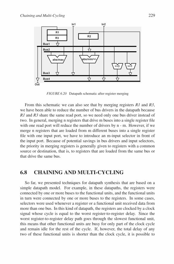
Chaining and Multi-Cycling 229
H
O u t
I n 1 I n 2
R1R2
> > 3 > > 1
B u s 1
a b s /ma x a b s /mi n /+ /-
B u s 2
B u s 3
B u s 4
R3
FIGURE 6.20 Datapath schematic after register merging
From this schematic we can also see that by merging registers R1 and R3,we have been able to reduce the number of bus drivers in the datapath becauseR1 and R3 share the same read port, so we need only one bus driver instead oftwo. In general, merging n registers that drive m buses into a single register filewith one read port will reduce the number of drivers by n - m. However, if wemerge n registers that are loaded from m different buses into a single registerfile with one input port, we have to introduce an m-input selector in front ofthe input port. Because of potential savings in bus drivers and input selectors,the priority in merging registers is generally given to registers with a commonsource or destination, that is, to registers that are loaded from the same bus orthat drive the same bus.
6.8 CHAINING AND MULTI-CYCLINGSo far, we presented techniques for datapath synthesis that are based on a
simple datapath model. For example, in these datapaths, the registers wereconnected by one or more buses to the functional units, and the functional unitsin turn were connected by one or more buses to the registers. In some cases,selectors were used whenever a register or a functional unit received data frommore than one bus. In this kind of datapath, the registers are clocked by a clocksignal whose cycle is equal to the worst register-to-register delay. Since theworst register-to-register delay path goes through the slowest functional unit,this means that other functional units are busy for only part of the clock cycleand remain idle for the rest of the cycle. If, however, the total delay of anytwo of these functional units is shorter than the clock cycle, it is possible to

230 Hardware Synthesis
connect them in series and thereby perform two operations in a single clockcycle. This same principle can be extended to more than two functional unitsif the datapath has a longer clock cycle. This technique of connecting units inseries is called chaining, since two or more units would be chained togetherwithout a register between them, thus creating a larger combinatorial unit thatcan compute assignments with two or more operations. Whenever we use thistechnique, a variable assignment statement in the FSMD model will containtwo or more operators on the right-hand side of the statement.
In 2
S0a = I n 1b = I n 2
0
1
Star t = 1
S1
S2
S3
S4
S5
S6
t1 = |a|t2 = |b|
t5 = x – t3
x = m ax ( t1 , t2 )t3 = m ax ( t1 , t2 )> > 3t4 = m i n ( t1 , t2 )> > 1
t6 = t4 + t5
t7 = m ax ( t6 , x )
D o n e = 1O u t = t7
(a) FSMD model for functional unitchaining
In 2
S0a = I n 1b = I n 2
0
1
Star t = 1
S1
S2
S3
S4
S5
S6
t1 = |a|t2 = |b|
t5 = x – t3t4 = [m i n ( t1, t2 ) > > 1]
x = m ax ( t1 , t2 )t3 = m ax ( t1 , t2 )> > 3[t4]= m i n ( t1 , t2 )> > 1
t6 = t4 + t5
t7 = m ax ( t6 , x )
D o n e = 1O u t = t7
(b) FSMD model for functional unitmulti-cycling
FIGURE 6.21 Modified FSMD models for SRA algorithm
To demonstrate chaining, we use a modified FSMD model of SRA algorithm,as shown in Figure 6.21(a). Note that this model merges two states (S2 and S3)from the previous FSMD model into one state (S2). As you can see, this meansthat three assignment statements will be executed in state S2 of Figure 6.21(a);

Chaining and Multi-Cycling 231
the first of these statements requires one binary operation (maximum), whilethe other two statements require two operations each. More specifically, thenew value would be assigned to t3 by computing the maximum of t1 and t2 andthen shifting the result to the right by three positions. At the same time, thenew value for t4 will be obtained by computing the minimum of t1 and t2 andthen shifting the result one position to the right. Since shifting to the right bythree or one positions incurs no delay, the clock cycle for this chained datapathwould be no longer than the original clock cycle. On the other hand, since thisFSMD model has only seven states instead of the eight states in the originalmodel, we would conclude that this modified datapath can perform the SRAalgorithm 12.5% faster.
In1
R1 R2 R3
> > 1
B u s 1
a b s /ma x
B u s 2
B u s 3
B u s 4
> > 3
In2
O u t
a b s /mi n/+ /-
FIGURE 6.22 Datapath with chained functional units
The new datapath schematic with the chained units is shown in Figure 6.22.Note that we had to create an additional connection from the right shifter toregister R3, so as to concurrently store the new values for variables x, t3, and t4that were generated in state S2. Though chaining allows us to concatenate fasterunits, there are instances in which we must use units which are slower, takingmore than one clock cycle to generate results, but which are less expensive. Thistechnique is called multi-cycling, and these slower units are called multi-cycleunits. For obvious reasons, such units can be used only for the non-criticalpaths through the FSMD model. For example, in Figure 6.21(a), variable t4will be assigned a new value (min (t1, t2) >> 1) in state S2, but this newvalue will not be used until state S4. In this case, then, we could use a unit thattakes two clock cycles to compute the minimum value, and chain this unit witha right shifter that takes no time to generate its result.
Such a multi-cycling arrangement is shown in Figure 6.21(b), in which theFSMD model for the SRA has been modified by the introduction of square
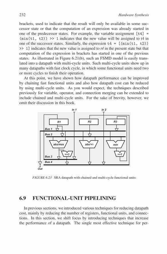
232 Hardware Synthesis
brackets, used to indicate that the result will only be available in some suc-cessor state or that the computation of an expression was already started inone of the predecessor states. For example, the variable assignment [t4] =
(min(t1, t2)) >> 1 indicates that the new value will be assigned to t4 inone of the successor states. Similarly, the expression t4 = [(min(t1, t2))
>> 1] indicates that the new value is assigned to t4 in the present state but thatcomputation of the expression in brackets has started in one of the previousstates. As illustrated in Figure 6.21(b), such an FSMD model is easily trans-lated into a datapath with multi-cycle units. Such multi-cycle units show up inmany datapaths with fast clock cycle, in which some functional units need twoor more cycles to finish their operation.
At this point, we have shown how datapath performance can be improvedby chaining fast functional units and also how datapath cost can be reducedby using multi-cycle units. As you would expect, the techniques describedpreviously for variable, operator, and connection merging can be extended toinclude chained and multi-cycle units. For the sake of brevity, however, weomit their discussion in this book.
In 1
R1 R2 R3
B u s 1
a b s /+ /-
B u s 2
B u s 3
B u s 4
In 2
O u t
a b s /ma x mi n
> > 3 > > 1
FIGURE 6.23 SRA datapath with chained and multi-cycle functional units
6.9 FUNCTIONAL-UNIT PIPELININGIn previous sections, we introduced various techniques for reducing datapath
cost, mainly by reducing the number of registers, functional units, and connec-tions. In this section, we shift focus by introducing techniques that increasethe performance of a datapath. The single most effective technique for per-
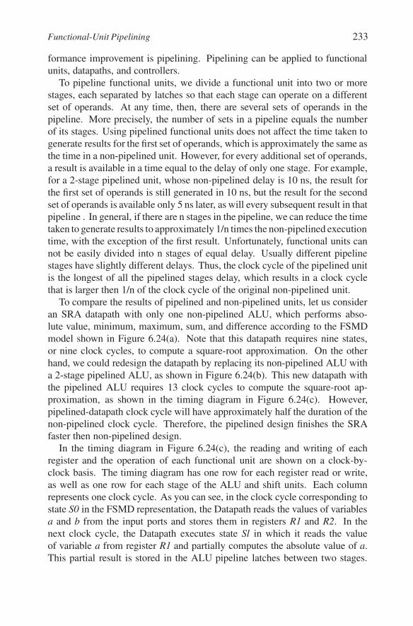
Functional-Unit Pipelining 233
formance improvement is pipelining. Pipelining can be applied to functionalunits, datapaths, and controllers.
To pipeline functional units, we divide a functional unit into two or morestages, each separated by latches so that each stage can operate on a differentset of operands. At any time, then, there are several sets of operands in thepipeline. More precisely, the number of sets in a pipeline equals the numberof its stages. Using pipelined functional units does not affect the time taken togenerate results for the first set of operands, which is approximately the same asthe time in a non-pipelined unit. However, for every additional set of operands,a result is available in a time equal to the delay of only one stage. For example,for a 2-stage pipelined unit, whose non-pipelined delay is 10 ns, the result forthe first set of operands is still generated in 10 ns, but the result for the secondset of operands is available only 5 ns later, as will every subsequent result in thatpipeline . In general, if there are n stages in the pipeline, we can reduce the timetaken to generate results to approximately 1/n times the non-pipelined executiontime, with the exception of the first result. Unfortunately, functional units cannot be easily divided into n stages of equal delay. Usually different pipelinestages have slightly different delays. Thus, the clock cycle of the pipelined unitis the longest of all the pipelined stages delay, which results in a clock cyclethat is larger then 1/n of the clock cycle of the original non-pipelined unit.
To compare the results of pipelined and non-pipelined units, let us consideran SRA datapath with only one non-pipelined ALU, which performs abso-lute value, minimum, maximum, sum, and difference according to the FSMDmodel shown in Figure 6.24(a). Note that this datapath requires nine states,or nine clock cycles, to compute a square-root approximation. On the otherhand, we could redesign the datapath by replacing its non-pipelined ALU witha 2-stage pipelined ALU, as shown in Figure 6.24(b). This new datapath withthe pipelined ALU requires 13 clock cycles to compute the square-root ap-proximation, as shown in the timing diagram in Figure 6.24(c). However,pipelined-datapath clock cycle will have approximately half the duration of thenon-pipelined clock cycle. Therefore, the pipelined design finishes the SRAfaster then non-pipelined design.
In the timing diagram in Figure 6.24(c), the reading and writing of eachregister and the operation of each functional unit are shown on a clock-by-clock basis. The timing diagram has one row for each register read or write,as well as one row for each stage of the ALU and shift units. Each columnrepresents one clock cycle. As you can see, in the clock cycle corresponding tostate S0 in the FSMD representation, the Datapath reads the values of variablesa and b from the input ports and stores them in registers R1 and R2. In thenext clock cycle, the Datapath executes state Sl in which it reads the valueof variable a from register R1 and partially computes the absolute value of a.This partial result is stored in the ALU pipeline latches between two stages.

234 Hardware Synthesis
In 2Done = 1O u t = t7
t1 = |a|
x = m ax ( t1 , t2 )t3 = m ax ( t1 , t2 )> > 3
t4 = m i n( t1 , t2 )> > 1
t6 = t4 + t5
t7 = m ax ( t6 , x )
Star t
a = I n1b = I n2
S0
0
1S1
S2
S4
S6
S7
S8
t5 = x – t3S5
t2 = |b|S3
(a) FSMD model
In1
R1 R2 R3
> > 1
B u s 1B u s 2
B u s 3B u s 4
> > 3
In2
O u t
2-s t a g e A LU
(b) Datapath with 2-stage pipelined ALU
t7
m ax
NO
t7
t7S 8
T 6
+
NO
m ax
t6XS 7
t5
> > 1-
NO
+t4t5
S 6
W r i t e Ou tt4W r i t e R 3
> > 3m i n-
t3XS 5
ba
S 0
t1
| b|
b
S 2
| a|
aS 1
m ax
t2t1S 3
t2
NO
t3X
m axm i n
t2t1S 4
W r i t e R 2W r i t e R 1S h i f t e r s
A L U s t a g e 2A L U s t a g e 1R e a d R 3R e a d R 2R e a d R 1
t7
m ax
NO
t7
t7S 8
T 6
+
NO
m ax
t6XS 7
t5
> > 1-
NO
+t4t5
S 6
W r i t e Ou tt4W r i t e R 3
> > 3m i n-
t3XS 5
ba
S 0
t1
| b|
b
S 2
| a|
aS 1
m ax
t2t1S 3
t2
NO
t3X
m axm i n
t2t1S 4
W r i t e R 2W r i t e R 1S h i f t e r s
A L U s t a g e 2A L U s t a g e 1R e a d R 3R e a d R 2R e a d R 1
(c) Timing diagram
FIGURE 6.24 Functional unit pipelining
Then, in the next clock cycle, the Datapath finishes the computation of |a| andassigns this value to variable t1, which is stored in register R1. At the sametime, the Datapath also initiates the computation of |b| specified in state S2, andstoring the partial result of this computation in the pipeline latches. Thus in thisclock cycle both stages of the pipelined ALU are active, although they processdifferent operands. In next clock cycle, the Datapath finishes computation of|b| and assigns it to variable t2 stored in register R2. Note that at this point the

Datapath Pipelining 235
Datapath cannot yet initiate the next operation because it requires the value oft2, which has not yet been loaded in register R2. Therefore, no operation isscheduled to start in fourth clock cycle and operation specified in state S3 isdelayed by one clock cycle. In a similar fashion, the Datapath starts execution ofmaximum, minimum, and subtraction operations in the fifth, sixth, and seventhclock cycles, and completes these operations, together with the shifts, in clockcycles six, seven, and eight. It cannot start the addition specified in state S7,since it must wait for the availability of the value assigned to t5. Similarly, itstarts the maximum operation in eleventh clock cycle with result being writteninto register R1 in the next clock cycle. Finally, the Datapath uses the thirteenthclock cycle to output the result.
According to this timing diagram, the SRA algorithm requires 13 clock cyclesto complete. As mentioned above, however, two of these clock cycles are equalto one clock cycle of the non-pipelined design, which means that the datapathwith the pipelined ALU computes the square-root approximation in six and ahalf clock cycles instead of the nine needed by the non-pipelined design, whichis 28% faster than the non-pipelined design. Note that this pipelined datapathcan outperform any non-pipelined design described in previous sections.
6.10 DATAPATH PIPELININGJust as with a functional unit, we can pipeline the whole datapath by inserting
registers in some coordinated fashion on every register-to-register path. Thebest way to pipeline a datapath is to divide the register-to-register delay intostages, which is easiest to achieve by inserting registers at the inputs and outputsof the functional units. A pipelined datapath for the SRA computation is shownin Figure 6.25(a). The register-to-register path is divided into three stages:registers to ALU input, ALU input to ALU output, and ALU output back toregisters. Note that ALU by itself can be also pipelined as described in previoussection.
In the timing diagram in Figure 6.25(b), the reading and writing of eachregister and the operation of each functional unit are shown on a clock-by-clock basis. The timing diagram has one row for each register read or write, aswell as one row for the ALU input and output registers and shift units. Eachcolumn represents one clock cycle where the column headings indicate the stateof the FSMD model that is initiated in that clock cycle or if no state is initiatedin that clock cycle. As you can see, in the first clock cycle corresponding tostate S0 in the FSMD representation in Figure 6.24(a), the datapath reads thevalues of variables a and b from the input ports and stores them in registersR1 and R2. In the next clock cycle, the datapath executes state S1, in whichit reads the value of variable a from register R1 and stores it in the ALU input
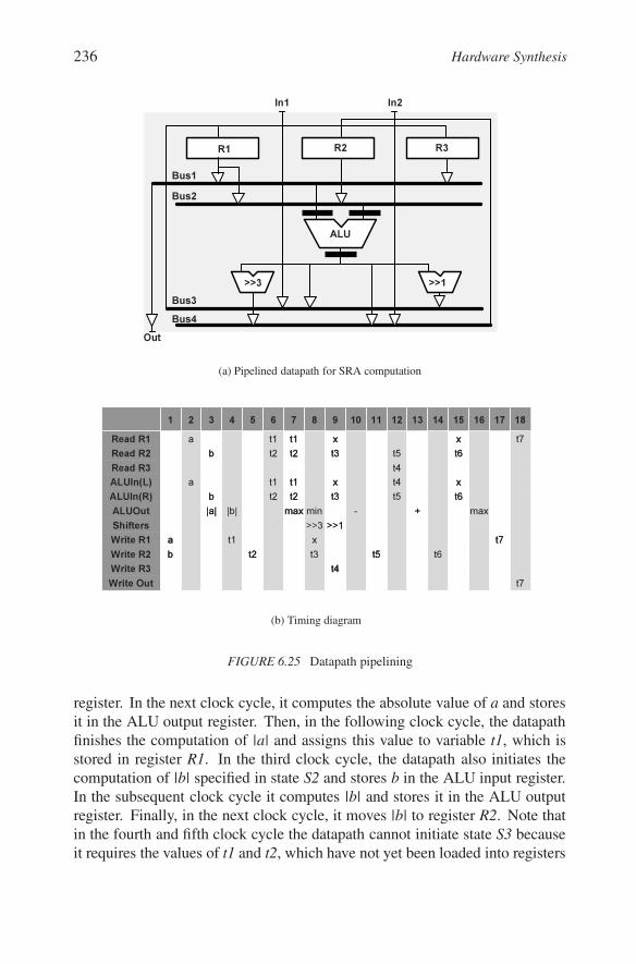
236 Hardware Synthesis
In1
R1 R2 R3
> > 1
B u s 1
B u s 2
B u s 3B u s 4
> > 3
In2
O u t
A L U
(a) Pipelined datapath for SRA computation
t6t5t3t2t2bALUIn(R)
t7
17
t7
t718
x
t6x15
m ax
16
t1
| b|
4
t2
5
t6
14
t4t4t5
12
+
13
-
10
t5
11
W r i t e O u tt4W r i t e R3
> > 1
x
t3x9
ba
1
| a|
b
3
a
a2
m ax
t1
t2t17
t1
t2t16
t3x
> > 3m i n
8
W r i t e R2W r i t e R1S h i f t e r sALUO u t
ALUIn(L)Re a d R3Re a d R2Re a d R1
t6t5t3t2t2bALUIn(R)
t7
17
t7
t718
x
t6x15
m ax
16
t1
| b|
4
t2
5
t6
14
t4t4t5
12
+
13
-
10
t5
11
W r i t e O u tt4W r i t e R3
> > 1
x
t3x9
ba
1
| a|
b
3
a
a2
m ax
t1
t2t17
t1
t2t16
t3x
> > 3m i n
8
W r i t e R2W r i t e R1S h i f t e r sALUO u t
ALUIn(L)Re a d R3Re a d R2Re a d R1
(b) Timing diagram
FIGURE 6.25 Datapath pipelining
register. In the next clock cycle, it computes the absolute value of a and storesit in the ALU output register. Then, in the following clock cycle, the datapathfinishes the computation of |a| and assigns this value to variable t1, which isstored in register R1. In the third clock cycle, the datapath also initiates thecomputation of |b| specified in state S2 and stores b in the ALU input register.In the subsequent clock cycle it computes |b| and stores it in the ALU outputregister. Finally, in the next clock cycle, it moves |b| to register R2. Note thatin the fourth and fifth clock cycle the datapath cannot initiate state S3 becauseit requires the values of t1 and t2, which have not yet been loaded into registers

Control and Datapath Pipelining 237
R1 and R2. Therefore, no operation is scheduled to start in the fourth or fifthclock cycles. Thus, the operations specified in state S3 are delayed by two clockcycles to start in the sixth clock cycle and finish in the eight clock cycle. In asimilar fashion, the datapath starts execution the state S4 in seventh clock cyclesand completes it, together with the shift operation, in the ninth clock cycle. Itcan start the subtraction operation specified in state S5, in the same clock cyclesince the values of variables to x and t3 are available in registers R1 and R3.
From the above description we can see, that this datapath needs three clockcycles to finish any operation specified in any state of the FSMD model and mayrequire two no-operation (NO) cycles if there is a data dependency between twooperations in the two succeeding states in the FSMD definition. In other words,it requires two NO cycles if a variable is assigned a value in one state of theFSMD description and used in the next state of the same description.
According to the timing diagram in Figure 6.25(b), this SRA algorithm re-quires 18 clock cycles to complete. As mentioned above, however, three of theseclock cycles are approximately equal to one clock cycle of the non-pipelineddesign, which means that the pipelined datapath in Figure 6.25(a) computes thesquare-root approximation in six clock cycles instead of the nine needed by thenon-pipelined design, so it arrives at the result 30% faster than a non-pipelinedSRA data path. Note that datapath pipelining described in this section canoutperform functional unit pipelining that has been described in the previoussection. In general, combining both types of pipelining may result in greaterperformance improvement than for each type of pipelining by itself. However,adding more pipeline stages may not be profitable in case of the SRA examplesince SRA does not have enough operations that can be executed concurrently.In general, the number of pipeline stages is equal to the number of operationsthat can be executed concurrently. If there is not enough concurrency, thepipeline has to wait for data to become available by performing no-operationcycles.
6.11 CONTROL AND DATAPATH PIPELININGIn previous sections, we discussed two methods for improving performance
through pipelining techniques that reduce the register-to-register delay. It isimportant to note, however, that the longest register-to-register delay can beusually found in the control unit. This critical path through the controllerdetermines the length of the clock cycle or clock period. Consequently, if wewant to improve performance by shortening the clock cycle, it would makesense to divide the critical path through the controller into pieces and insertregisters between them. In Figure 6.26(b), for example, registers are insertedin three difference places. First, we introduce a Status Register (SR) between
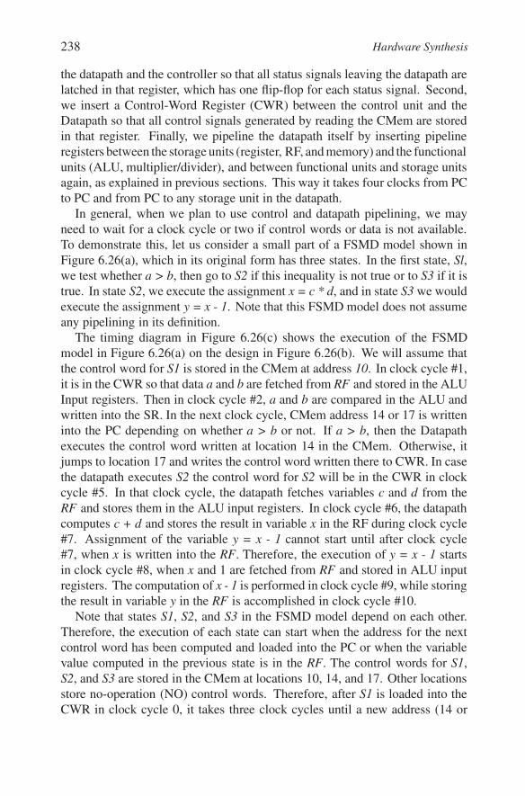
238 Hardware Synthesis
the datapath and the controller so that all status signals leaving the datapath arelatched in that register, which has one flip-flop for each status signal. Second,we insert a Control-Word Register (CWR) between the control unit and theDatapath so that all control signals generated by reading the CMem are storedin that register. Finally, we pipeline the datapath itself by inserting pipelineregisters between the storage units (register, RF, and memory) and the functionalunits (ALU, multiplier/divider), and between functional units and storage unitsagain, as explained in previous sections. This way it takes four clocks from PCto PC and from PC to any storage unit in the datapath.
In general, when we plan to use control and datapath pipelining, we mayneed to wait for a clock cycle or two if control words or data is not available.To demonstrate this, let us consider a small part of a FSMD model shown inFigure 6.26(a), which in its original form has three states. In the first state, Sl,we test whether a > b, then go to S2 if this inequality is not true or to S3 if it istrue. In state S2, we execute the assignment x = c * d, and in state S3 we wouldexecute the assignment y = x - 1. Note that this FSMD model does not assumeany pipelining in its definition.
The timing diagram in Figure 6.26(c) shows the execution of the FSMDmodel in Figure 6.26(a) on the design in Figure 6.26(b). We will assume thatthe control word for S1 is stored in the CMem at address 10. In clock cycle #1,it is in the CWR so that data a and b are fetched from RF and stored in the ALUInput registers. Then in clock cycle #2, a and b are compared in the ALU andwritten into the SR. In the next clock cycle, CMem address 14 or 17 is writteninto the PC depending on whether a > b or not. If a > b, then the Datapathexecutes the control word written at location 14 in the CMem. Otherwise, itjumps to location 17 and writes the control word written there to CWR. In casethe datapath executes S2 the control word for S2 will be in the CWR in clockcycle #5. In that clock cycle, the datapath fetches variables c and d from theRF and stores them in the ALU input registers. In clock cycle #6, the datapathcomputes c + d and stores the result in variable x in the RF during clock cycle#7. Assignment of the variable y = x - 1 cannot start until after clock cycle#7, when x is written into the RF. Therefore, the execution of y = x - 1 startsin clock cycle #8, when x and 1 are fetched from RF and stored in ALU inputregisters. The computation of x - 1 is performed in clock cycle #9, while storingthe result in variable y in the RF is accomplished in clock cycle #10.
Note that states S1, S2, and S3 in the FSMD model depend on each other.Therefore, the execution of each state can start when the address for the nextcontrol word has been computed and loaded into the PC or when the variablevalue computed in the previous state is in the RF. The control words for S1,S2, and S3 are stored in the CMem at locations 10, 14, and 17. Other locationsstore no-operation (NO) control words. Therefore, after S1 is loaded into theCWR in clock cycle 0, it takes three clock cycles until a new address (14 or

Scheduling 239
S1
1 0a>b
x = c + d
y = x - 1
S2
S3
(a) FSMD modelexcerpt
ALU
R e g i s t e r
S e l e c t o r
R F M e m
B u s 2B u s 1
S t a t u sS i g n a l s
C o n t r o ls i g n a l s
/∗ ÷
R e g i s t e r
DataI n p u ts
D a t a p a t hData
O u tp u tsCW
R
PC C M e m
AG
SR
O f f s e t
C o n tr o l l e r
C o n tr o lI n p u ts
C o n tr o lO u tp u ts
B u s 3
(b) RTL design
14/16
N O133
15
N O144
2 0
x-1
199
y
2 010
19181716131211W r i t e P Ca> bW r i t e S R
1x1xS 3188
100
N O122
babaS 1111
c+ d
N O166
dcdcS 2155
x
N O177
W r i t e R FW r i t e A L U O u tW r i t e A L U I n ( R )W r i t e A L U I n ( L )R e a d R F ( R )R e a d R F ( L )R e a d C W RR e a d P C
C l o c k c y c l e #
(c) Timing diagram
FIGURE 6.26 Control and datapath pipelining
17) is loaded in the PC and one more clock cycle until the new control word isloaded into the CWR. Therefore, the datapath executes three NO control wordsstored at locations 11, 12, and 13 as it waits for a > b comparison to complete.Similarly, datapath, while waiting for variable x to be stored in RF, executestwo NO control words stored at locations 15 and 16 in the CMem.
From this simple example, we can see that control and datapath pipeliningdoes not help if there is control dependency (S2 depends on S1) or data depen-dency (S3 depends on S2). However, pipelining does help if there are at leastthree not dependent states in the FSMD model or three independent statementsin a BB. Control dependency is difficult to avoid since the next address is com-puted dynamically. But it is possible to minimize the number of NO words ina datapath with branch prediction, as long as the prediction is correct most ofthe times.
240 Hardware Synthesis
6.12 SCHEDULINGIn previous sections, we have demonstrated how to synthesize custom designs
that consist of a datapath and a control unit. In general, the synthesis is based onthe FSMD model, which explicitly specifies states and the variable assignmentsto be performed in each state. Unfortunately, custom designs are usually basedon algorithms that have not been specified as FSMDs, but which instead havebeen described in a programming language or its CDFG, which, though itprovides control and data dependencies, does not support the concept of astate. These models must be converted to FSMD models during synthesis. Totransform an ordinary algorithm or CDFG into a cycle-accurate FSMD, we mustschedule the variable access and operations into states under either resource ortime constraints. In this section, we demonstrate two types of this scheduling,resource-constrained (RC) and time-constrained (TC), and give examples ofscheduling algorithms for each type [155, 45, 186, 128, 152, 34, 10, 156].
To perform scheduling, we must first convert a program into a representa-tion, such as CDFG, which explicitly shows the control dependencies amongstatements as well as the data dependencies among variable values. In Fig-ure 6.26(a) and Figure 6.26(b), we show a C-language flowchart and its cor-responding CDFG for the SRA algorithm. Such a CDFG representation isfrequently used by scheduling algorithms, since a scheduled CDFG is equiv-alent to a cycle-accurate FSMD. As we mentioned earlier, a CDFG can bescheduled using resource or timing constraints. For the former, we can specifythe resource constraints by the complete or partial number and type of func-tional and storage units, and their connections, in the datapath. They can alsobe specified by giving a complete netlist of the datapath. For scheduling usingtiming constraints, the time constraints are specified as the number of states orclock cycles the datapath will need to execute all the operations on the longestpath through the given CDFG.
However, before we detail RC and TC scheduling algorithms, we must intro-duce as-soon-as-possible (ASAP) and as-late-as- possible (ALAP) schedulingalgorithms, which are frequently used by RC and TC scheduling algorithms todetermine operation priority and range for scheduling.
ASAP and ALAP algorithms assume, first, that each operation will takeexactly one clock cycle to execute, and second, that an unlimited number offunctional units or resources are available for each operation in each state.Because of these assumptions, both algorithms are constrained only by data de-pendencies. Within this context, the ASAP algorithm schedules each operationinto the earliest state in which all its operands are available. In other words, itscans the CDFG from top to bottom and assigns to each state all the nodes inthe graph whose predecessor or parent nodes have been already assigned into
Scheduling 241
0S tar t
t1=|a|t2=|b|
x=m ax(t1,t2)y=m i n (t1,t2)
t3=x> > 3t4=y> > 1t5=x-t3
t6=t4+t5t7=m ax(t6,x)
D o n e =1O u t=t7
a=I n 1b=I n 2
1
(a) Flowchart inC
0
1S t ar t
I n 1 I n 2
a b
a b
m i n
|a| |b|
m ax
> > 1 > > 3
-+
m ax
O u t D o n e1
(b) CDFG model
FIGURE 6.27 C and CDFG
previous states. Thus the ASAP algorithm generates a schedule that has theminimum number of states or, in other words, the shortest execution time.
In contrast to the ASAP approach, the ALAP algorithm schedules each oper-ation into the last possible state before its result is needed, the ALAP algorithm,using the length of the final schedule in the number of states as a constraint,schedules each operation into the last possible state before its result is needed.In other words, it scans the CDFG from the bottom to the top and assigns toeach state all the nodes whose successor or children nodes have been alreadyassigned into later states. If the required schedule length is equal to the lengthobtained by the ASAP algorithm, we can observe, that the ALAP algorithmschedules all the operations on the critical path through the dataflow graph intothe same states as the ASAP algorithm. The operations that are not on thecritical path are scheduled earlier than needed in the ASAP schedule and laterthan possible in the ALAP schedule. Therefore, ASAP and ALAP algorithmsgive us ranges of possible states for scheduling non-critical operations. Fur-

242 Hardware Synthesis
thermore, the range length determines the operation priority or urgency to betaken into account during scheduling.
In Figure 6.28(a) and (b), we have applied ASAP and ALAP scheduling tothe larger of the two BBs in Figure 6.26(b), limiting this demonstration to asingle BB for the sake of simplicity. Both schedules in Figure 6.12.1 requireseven states. We also see that all operations except min and »1 are on the criticalpath. These two operations are scheduled as early as possible (states S2 and S3)in the ASAP schedule and as late as possible (states S3 and S4) in the ALAPschedule.
The fact that ASAP and ALAP algorithms schedule operations on the crit-ical path to the same states can be used to separate critical from non-criticaloperations in general scheduling algorithms. In the above example, therefore,min and »1 are non-critical operations. The priority is always given to thoseoperations that are on the critical path, since delaying one of these operationsby one state would extend the schedule by one state and increase the executiontime. On the other hand, lower priority can be given to operations that are noton the critical path, since they have greater flexibility of being scheduled indifferent states and can be delayed without affecting the execution time of theentire CDFG.
An operation’s priority during scheduling can be measured by several differ-ent metrics. One of these metrics is the operation’s mobility, which is equal tothe number of states between the states assigned to that particular operation inASAP and ALAP schedules. In other words, if an operation, op, is scheduledin state Si in the ASAP schedule and in state Sk in the ALAP schedule, itsmobility, M(op), will be equal to k - i. Thus mobility defines the operation’sability to be postponed without an impact on the total execution time. This canbe used for prioritizing operations because states with higher mobility can begiven lower priority.
As an alternative measure of priority, we can use the criterion of operationurgency, which is equal to the distance in the number of states between the statein which the operation is available for scheduling and the state in which theoperation occurs in its ALAP schedule. In other words, if an operation, op, isavailable in state Sj but is not scheduled until state Sk in its ALAP schedule,that state’s urgency U(op) will be equal to k - j.
As a third measure of operation’s priority, we could consider how manyother operations use its result as an operand, or in other words, the numberof dependencies. This measure gives priority to operations that increase thenumber of operations available for scheduling in the future. There are severalother priority measures, but none of them works perfectly in all cases. In theory,we could use any number of priority metrics in any order to determine a priorityfor scheduling among several operations available at the same time.

Scheduling 243
6.12.1 RC SCHEDULINGOne of the most popular algorithms for RC scheduling is the list-scheduling
algorithm, which uses a ready list of operations that are available for scheduling.In this algorithm, the operations on the ready list are sorted by their mobilities,so that the operations with zero mobility will be placed at the top of the list whilethose operations with the greatest mobility will be placed at the bottom. In caseswhere two operations have the same mobility, priority is given to the operationwith the lower urgency number. If those are identical as well, the priorityis assigned randomly. In applying this list-scheduling algorithm, we take thefollowing steps in each state: assign the highest-priority operations from theready list to the available functional units, one at a time, then delete all theassigned operations from the list, and insert the newly schedulable operationsinto the list in the positions that correspond to their mobilities and urgencies.
Out
m i n
|a| |b|
m ax
> > 1 > > 3
-
+
m ax
Out
m i n
|a| |b|
m ax
> > 1
> > 3
-
+
m ax
S5
S6
S7
S2
S3
S4
m ax
|a| |b|
> > 3
m i n
+
m ax
0
0
1
1
0
0
Out
m i n
|a|
|b|
m ax
> > 1
> > 3
-
+
m ax
|b|0
0
0m i n
- > > 11
0
S8
S1
a b a b a b
(a) ASAP (b) ALAP (c) Ready list with nobil-ities
(d) RC schedule
FIGURE 6.28 ASAP, ALAP, and RC schedules for SRA
This list-scheduling algorithm is summarized in FIGURE 6.29. We demon-strate this list-scheduling algorithm on the dataflow graph of the BB in Fig-ure 6.27(b) under the assumption that we have only one arithmetic unit, whichcan perform absolute value, minimum, maximum, addition, and subtraction, in

244 Hardware Synthesis
addition to two shift units. To perform RC scheduling with a list-schedulingalgorithm, we first generate ASAP and ALAP schedules, as shown in Fig-ure 6.28(a) and (b). Then we create a ready list for the first state, as shown inFigure 6.28(c), and compute the mobilities for the operations in that ready list.In our case, only operations |a| and |b| are available in the first state. Sincethese operations have the same mobility [M(|a|) = M(|b|) = 0], we select theirorder randomly and schedule |a| first. Since scheduling |a| does not free anymore operations for scheduling, we do not change the ready list at this time.Therefore, we must schedule |b| in state S2, which allows us to add max andmin operators to the ready list. Since the max operator is on the critical path,it has a mobility M(max) = 0, which gives it priority over the min operator,which has mobility M(min)= 1. Therefore, we would schedule max into stateS3, which allows us to add »3 to the ready list. Since its mobility M(»3) = 0,this operator should be placed at the top of the ready list. At this point we haveone ALU and two shifters available, so we can now schedule both the (»3) andthe min operations in state S4. We then update the ready list, adding - and »1,which can both be scheduled into state S5. That allows us to schedule + intostate S6 and max into state S7, and finally, output the result in state S8. Thefinal RC schedule is shown in Figure 6.28(d).
As we have shown, the goal of the RC scheduling algorithm is to schedule ineach state as many operations as possible given the limited number of availableunits or connections. When more operations are available than there are unitsor connections, we must use a priority metric, such as mobility or urgency.In our example, we obtained a schedule that requires one more state than theASAP or ALAP schedules, but at lower cost since we used only one ALUand two shifters, while the ASAP and ALAP schedules required two ALUsand two shifters. The simple algorithm in Figure 6.29 was used to demonstrateprinciples of list scheduling. There are many more sophisticated list-schedulingin the literature that can take advantage of controller and datapath architectureas well as the information in the input model.
6.12.2 TC SCHEDULINGIn many cases, the primary goal of design optimization is to improve the
performance, not the cost, since a datapath must execute a given code in a fixedamount of time. When execution time is our priority, we use time-constrained(TC) scheduling, which generates a schedule comprising a particular number ofstates while attempting at the same time to minimize the number of functionalunits it requires in the datapath. This goal is achieved by creating a probability-distribution graph and using it to schedule operations into states one at thetime so that the largest sum of probabilities for each operator and each state isminimal.

Scheduling 245
no
P e r f r om A S A P
P e r f r om A L A P
D e t e r m i ne m ob i l i t i e s
C r e a t e r e a d y l i s t
S or t r e a d y l i s t b y m ob i l i t i e s
S c h e d u l e op s f r om r e a d y l i s t
D e l e t e s c h e d u l e d op s f r om r e a d y l i s t
A d d ne w op s t o r e a d y l i s t
I nc r e m e nt s t a t e i nd e x
A l l op s s c h e d u l e d ?
y e s
FIGURE 6.29 RC algorithm
no
P e r f r om A S A P
P e r f r om A L A P
D e t e r m i ne m ob i l i t i e s r a ng e s
C r e a t e p r ob a b i l i t y d i s t r i b u t i on g r a p h s
A l l op s s c h e d u l e d ?
y e s
A l l op s s c h e d u l e d ?
y e s
S c h e d u l e op s f r om r e a d y l i s t
S c h e d u l e op s f r om r e a d y l i s t
FIGURE 6.30 TC algorithm
To use TC scheduling, we first apply the ASAP and ALAP scheduling algo-rithms to determine the mobility range for each operation. Having establishedthese ranges, we then assign to each operation an equal probability of beingscheduled in each state in its range. Obviously, for each operation, the sum ofall these probabilities over the entire range equals 1.
Once we have calculated these probabilities, we can then create probabilitydistribution graphs, which define the probability sums in each state for eachset of compatible operations. In other words, these probability sums determinethe number of functional units of each type required in each state. Using thisinformation, we can attempt to minimize the number of functional units byselecting an operation and scheduling it in the state that will reduce the largestprobability sum for this operation type in the distribution graph. If reductionis not possible, we can select an operation and schedule it in the state in whichit will minimally increase the probability sum. The algorithm terminates onlywhen all operations have been scheduled as shown in Figure 6.30.

246 Hardware Synthesis
Out
m i n
|a| |b|
m ax
> > 1 > > 3
-
+
m ax
Out
m i n
|a| |b|
m ax
> > 1
> > 3
+
m ax
m i n
|a|
|b|
m ax
> > 1
> > 3
-
+
m ax
S5
S6
S7
S1
S3
S4
S8
S2
a b a b a b
Out(a) A S A P (b) A L A P (c) T C s ch e d u l e
-
(a) ASAP (b) ALAP (c) TC schedule
FIGURE 6.31 ASAP, ALAP, and RC schedules for SRA
We demonstrate TC scheduling on the dataflow graph of the larger BB inFigure 6.27(b), and for comparison purposes we set a goal of eight states forthe complete schedule, as this was the schedule length that we obtained withRC scheduling using one ALU and two shift units. In our first step, we createASAP and ALAP schedules, as shown in Figure 6.31(a) and (b).
From these schedules, we can compute mobility ranges, concluding thatthe mobility range for all the operators except »1 and min would be 2. Inother words, the probability of each of these operators being scheduled in anyparticular state in its range would be 0.5. Since the operators min and »1each have a range of three states, the probability of their being scheduled in anyparticular states within that range would be 0.33. These individual probabilitiesare combined in Figure 6.32(a) into two distribution graphs that we then usefor minimizing the number of ALUs and shift units.
As you can see from the distribution graphs for ALUs and shift units, schedul-ing any operation into a particular state increases the probability sum in thatstate and therefore the number of units required, except in state S7, where the

Scheduling 247
1.8 3
S5
S6
S7
S1
S2
S3
S4
|a| |b|
max
min
-
+
max
>>1 >>
3
1.0
.8 3
.8 3
1.0
1.0
.5
.8 3
.8 3
.3 3
A U u n i t s
P r o b a b i l i t y s u m /s t a t e
S h i f t u n i t s
(a) Initial probability distributiongraph
1.33
S5
S6
S7
S1
S2
S3
S4
|a| |b|
m ax
min
-
m ax
>>1 > > 3
1.0
1.33
.33
1.0
1.0
1.0
A U u n i t s
P r o babi l i t y s u m /s t at e
S h i f t u n i t s
+(b) Graph after max, +, and -were scheduled
1.0
S5
S6
S7
S1
S2
S3
S4
|a| |b|
m ax
m i n
-
m ax
> > 1
> > 3
1.0
1.0
1.0
1.0
1.0
A U u n i t s
P r o babi l i t y s u m /s t at e
S h i f t u n i t s
+
1.0
1.0
1.0
(c) Graph after max, +, -, min, »3, and»1 were scheduled
1.0
S5
S6
S7
S1
S2
S3
S4
|a|
|b|
m ax
m i n
-
m ax
> > 1
> > 3
1.0
1.0
1.0
1.0
1.0
A U u n i t s
P r o babi l i t y s u m /s t at e
S h i f t u n i t s
+
1.0
1.0
1.0
(d) Distribution graph for final sched-ule
FIGURE 6.32 Distribution graphs for TC scheduling of the SRA example
probability sum is only 0.5. Therefore, we schedule the max operator in state S7,which increases the probability sum to 1.0. For the same reason, we schedule +in state S6 and - in state S5. At this point we have the option of scheduling maxor min in state S3. As you can see, however, scheduling max there decreases

248 Hardware Synthesis
the probability sum in state S2 to 1.33, while scheduling min would decreasesthe probability sum to 1.5, so we schedule max in state S3 and decrease thisprobability sum as much as possible. Once max has been scheduled in state S3,we have to schedule »3 into state S4 since »3 has to use the result of the maxoperation as its input. In Figure 6.32(b), you can see the distribution graphsthat correspond to the partial schedule we have developed by this point in thealgorithm. Using the same criteria as before, we then schedule the min opera-tion into state S4 and »1 into state S5, producing the distribution graph shownin Figure 6.32(c).
Finally, when we try to schedule either |a| or |b|, we have to increase theprobability sum of either S1 or S2, but this increase is only temporary sincewhen both have been scheduled, the probability sum in each state equals 1.0for the ALU as well as for the shifter unit. In other words, we have shown thatthe CDFG from Figure 6.27(b) can be scheduled into nine states using only oneALU and one shift unit, although we will eventually use two separate shiftersinstead of one shift unit, since their cost and delay is almost zero.
Although in this case the TC algorithm produced the same schedule as the RCalgorithm, in more complex cases these two algorithms will typically producedifferent schedules. As a rule, we would usually select the algorithm that bettermatches the primary goal of our design, using RC scheduling to satisfy costconstraints and TC scheduling when we need to satisfy performance constraints.
6.13 INTERFACE SYNTHESISIn the previous sections we described different tasks of HW synthesis design
flow shown in Figure 6.1. These tasks included RTL component allocation,variable, operation and connectivity binding, pipelining, scheduling, and RTLgeneration. In this section we will try to demonstrate the task of integratingsuch custom HW component into the system platform whose generation wasdescribed in Chapter 4. Similarly to software synthesis described in Chapter 5we have to combine the application processes allocated to the HW componentwith communication channels needed for message transfers between differentcomponents in the platform.
First, we need to extract the process code and channel code from the systemTLM model and combine them into an input such as C or CDFG for the HWsynthesis tools. However, the synthesized HW component may use differentclock cycle then the bus protocol that is used for the communication amongcomponents in the platform. To avoid this unusual constraint to HW compo-nent synthesis we may want to separate sending a message with bus protocolfrom computation performed in the HW component. For this reason we need
Interface Synthesis 249
to introduce a special bus interface that sends the message produced by HWcomponent to another platform component with the bus protocol timing.
Second, the main advantage of automatic HW synthesis is its ability to usean untimed code as an input and generate a cycle-accurate RTL description.As a result, the designer is relieved from defining cycle timing. While thisscheduling freedom is beneficial for implementing application and some ofthe communication code it becomes severely limited by imposing protocoltiming constraints on synthesis tasks. In order to avoid this constraint andstill guarantee bus protocol timing is to not synthesize the bus interface, but toinstantiate a pre-implemented and tested bus interfaces from a library. In thiscase, a special driver layer is used to interface the synthesized application andcommunication code and the pre-implemented bus interface.
Figure 6.33 outlines an implementation stack for a custom HW component.This implementation stack is partly contained in the system model, which wehave described in Chapter 3. The stack generation is similar to the softwaresynthesis described in Chapter 5. The shown HW component includes anapplication process P2 which has been combined with a communication stack,that models communication with external components. The stack layers aredivided into three groups based on the timing constraints for the generatedimplementation.
ApplicationP r e s e ntationS e s s ionT r ans por tN e tw or kL inkS tr e am
P2
M ACP r otocolP h y s ical
HW
(a) F r e e l y s ch e d u l abl e co d e
(b) S ch e d u l e co n s t r ai n t co d e
(c) R T L bu s i n t e r f ace
FIGURE 6.33 HW Synthesis timing constraints
(a) Freely schedulable code. Most of the code inside a custom hardwarecomponent is freely schedulable. This includes the actual application codeprocess P2 and most of the communication stack down to a set of MAClayer calls for sending and receiving a word or packet on the bus.
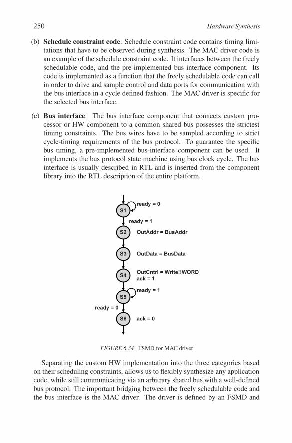
250 Hardware Synthesis
(b) Schedule constraint code. Schedule constraint code contains timing limi-tations that have to be observed during synthesis. The MAC driver code isan example of the schedule constraint code. It interfaces between the freelyschedulable code, and the pre-implemented bus interface component. Itscode is implemented as a function that the freely schedulable code can callin order to drive and sample control and data ports for communication withthe bus interface in a cycle defined fashion. The MAC driver is specific forthe selected bus interface.
(c) Bus interface. The bus interface component that connects custom pro-cessor or HW component to a common shared bus possesses the strictesttiming constraints. The bus wires have to be sampled according to strictcycle-timing requirements of the bus protocol. To guarantee the specificbus timing, a pre-implemented bus-interface component can be used. Itimplements the bus protocol state machine using bus clock cycle. The businterface is usually described in RTL and is inserted from the componentlibrary into the RTL description of the entire platform.
S5
S4
S3
S1
S2
S6
O u t A d d r = B u s A d d r
O u t D a t a = B u s D a t a
O u t C n t r l = W r i t e ! ! W O R Da c k = 1r e a d y = 1
a c k = 0r e a d y = 0
r e a d y = 1
r e a d y = 0
FIGURE 6.34 FSMD for MAC driver
Separating the custom HW implementation into the three categories basedon their scheduling constraints, allows us to flexibly synthesize any applicationcode, while still communicating via an arbitrary shared bus with a well-definedbus protocol. The important bridging between the freely schedulable code andthe bus interface is the MAC driver. The driver is defined by an FSMD and

Interface Synthesis 251
callable from within the synthesized code. The FSMD defines explicit input andoutput registers as well as control signals, which are used to interface customHW and bus interface components.
ALU
R e g R F M e m
B u s 2B u s 1
S t a t u ss i g n a l s
C o n t r o ls i g n a l s
/∗ ÷
PC C M e m
AG
o f f s e t
C o n t r o l l e r
Control
a c k
A d d re s sDA
TA
DATA
ADDR
ESS
W ri te Q u e u e
R e a d Q u e u e
D a t a p a t h
Bus I
nterfa
ce O u tp u t log i c
I np u t log i c
SR
B u s 3 B u s 4
S e l e c t o r
Selector
D AT AAD D R E S SC O N T R O LG R AN TR E Q UE S T
C o n t r o ls i g n a l s
I N C
Appli
catio
n Pro
cess
or
r e a d y O u tC n trl O u tA d d r O u tD a ta I n D a ta
FIGURE 6.35 Custom HW component with bus interface
Figure 6.34 shows a FSMD model of a MAC driver example for communica-tion with a bus interface in a double handshake fashion. It uses output registersOutAddr, OutData and OutCntrl. In addition, it uses control signals ready andack. This driver can be invoked from the synthesized communication codeas shown in Figure 6.33, by calling the function busif send(), which thentriggers transferring BusWord to the address BusAddr. The driver first waitsuntil ready indicates that the bus interface is free for the next transfer. Thenin state S2, the driver loads the address register OutAddr, in state S3the dataregister OutData, and sets the a control register OutCntrl for writing a singleword on the bus in state S4. It also signals by setting ack that data is ready forthe bus transaction. The driver then waits until the bus interface responds bylowering ready that it has received the transfer request. The driver finishes the

252 Hardware Synthesis
transaction by lowering ack in state S6. At this point in time, the bus interfacemay start the bus transaction.
Figure 6.35 shows a synthesized custom HW component with a applica-tion processor on the top and a bus interface on the bottom. The applicationprocessor is composed of a controller and the datapath. The datapath’s microarchitecture is determined during the HLS which also includes the MAC driverfrom Figure 6.34. The custom application processor and bus interface are con-nected through the registers OutCntrl, OutAddr, OutData and InData, as wellas with the control signals ready and ack as indicated in Figure 6.35. The businterface is also composed of a controller and a data path. The datapath is sim-ple, as it only drives and samples the bus wires. The controller, implementedas an FSM, secures the bus protocol timing like one shown in Figure 6.36.
The code describing the user application is synthesized to execute on theapplication processor. Each call to the MAC driver triggers the execution of theMAC FSMD, as shown in Figure 6.34, and transfers data word or a packet intothe bus interface. The bus interface then executes the data transfer over the bususing the bus protocol like one shown in Figure 6.36.
Figure 6.36 illustrates writing a word using the protocol of the synchronous,pipelined AMBA AHB 2.0 [4]. To initiate the transfer, the bus interface firstrequests bus access in cycle 1, by raising REQUEST and then waits for GRANT,which appears during cycle 3. Subsequently, the bus interface drives CONTROLin cycle 4 indicating the transfer type, and also drives the ADDRESS bus withthe address given by the application in OutAddr. In cycle 5 of the pipelinedprotocol, the bus interface drives the write data bus WDATA with the data passedby the application code. The transfer completes in cycle 6, since the receivingslave drives READY. As a result of this bus transaction the user data has beentransfered from the application processor to the slave.
time [c y c l e]
GRANTC NTRO LAD D RE S S
W D ATARE AD Y
C L KRE Q U E S T
nonseq.,w or d0xA 000 0000
0x2F00 9 8 01
1 2 3 4 5 6
FIGURE 6.36 A typical bus protocol
The above described bus interface solves the problem of transferring data inand out of a synthesized custom HW component. The same solution can be usedto transfer data between any two components with different communication

Summary 253
protocols. This is particularly true in a complex platform with several busses.In this case we can combine two bus interface components into a bridge thatconverts one protocol into another. More complex conversion of differentlyconstructed messages can be accomplished with a transducer.
Processor1<clk1>
Processor2<clk2 >
C on t rol l er1<clk1>
C on t rol l er1<clk1>
C on t rol l er2<clk2 >
C on t rol l er2<clk2 >
Transducer
R e a d y 1A ck1
R e a d y 2A ck2
M em ory 1M em ory 1 M em ory 2M em ory 2
P E 1 P E 2B u s 1 B u s 2
I n t e r r u p t 2I n t e r r u p t 1
D a t a 1 D a t a 2
Q u eu e<clk3 >
FIGURE 6.37 Transducer structure
Transducer is a device for protocol transformation and routing messages.Messages may have any length and may use any format or protocol known tothe transducer. They are stored one message at the time in transducer queue.Each transducer consists of a queue and two message controllers, Controller1and Controller2, as shown in Figure 6.37. Each controller can write into andread from the queue. Both controllers and the queue may run under differentclocks. One controller receives the message with one protocol, decomposesthe message into words and stores it in the queue, while the other controllercomposes message from the queue and sends it out to proper destination underthe second protocol. Transducer also computes the new route if it is not encodedin the message.
Therefore, using bus interfaces, bridges and transducers we can construct amulti-bus or network-on-chip communication among variety of components ina multi purpose heterogeneous platform.
6.14 SUMMARYIn this chapter we have explained how to specify and generate HW compo-
nent design for some standard input models given by CDFG and FSMD models.In addition, we described several procedures for optimizing such designs, show-
254 Hardware Synthesis
ing how to merge variables and assign them to registers, how to merge registersinto register files or memories, how to merge operators and assign them tomultifunction units, and how to merge connections and create buses for eachgroup of connections. We also demonstrated how to optimize these implemen-tations for functional units of different speed by chaining fast functional unitsand multi-cycling slow units that take more than one clock cycle to produceresults.
In the later sections we introduced the concept of pipelining and showed howwe can improve performance by pipelining functional units, control units, orentire datapaths.
In the last section we demonstrated how to transform C programs or theircorresponding CDFGs to cycle-accurate FSMDs by scheduling the assignmentstatements into specific states. We described the two types of scheduling al-gorithms that we can use to accomplish scheduling. These algorithms reflectdifferent optimization goals: resource-constrained scheduling minimizes ex-ecution time for a given set of resources, while time-constrained schedulingminimizes the resources required for a given execution time.
In summary, this chapter presented a general methodology for specifyingHW components with different models and generating RTL implementationsfrom these models. There are several good references on the topic [178, 35,114, 61, 186, 139, 110, 45].
However there is lot of more work needed to improve design quality suchas control and datapath pipelining, synthesis optimization for different metricssuch as power, manufacturability, dependability, introduction of HLS or archi-tecture cells such as different controllers and datapaths to replace standard cellsand work on pre synthesis optimization and input re-coding for synthesis.