Embedded Software Design for the Canadian Advanced ... · Embedded Software Design for the Canadian...
93
Embedded Software Design for the Canadian Advanced Nanospace eXperiment Generic Nanosatellite Bus by Mark Matthew Paul Champion Dwyer A thesis submitted in conformity with the requirements for the degree of Masters of Applied Science Graduate Department of Aerospace Engineering University of Toronto © Copyright by Mark Matthew Paul Champion Dwyer 2009
Transcript of Embedded Software Design for the Canadian Advanced ... · Embedded Software Design for the Canadian...

Embedded Software Design for the Canadian Advanced Nanospace eXperiment Generic Nanosatellite Bus
by
Mark Matthew Paul Champion Dwyer
A thesis submitted in conformity with the requirements for the degree of Masters of Applied Science
Graduate Department of Aerospace Engineering University of Toronto
© Copyright by Mark Matthew Paul Champion Dwyer 2009
ii
Embedded Software Design for the Canadian Advanced
Nanospace eXperiment Generic Nanosatellite Bus
Mark Matthew Paul Champion Dwyer
Masters of Applied Science
Graduate Department of Aerospace Engineering University of Toronto
2009
Abstract
The Space Flight Lab (SFL) at the University of Toronto Institute for Aerospace Studies
(UTIAS) has developed an ambitious satellite program called the Canadian Advanced
Nanospace eXperiment (CanX). The newest generation of CanX missions are based on the
Generic Nanosatellite Bus (GNB). This bus was designed to accommodate many missions using
a single, common platform. Currently, there are three nanosatellite missions using the GNB
design. These missions include AISSat-1, CanX-3 (BRITE) and CanX-4&5. This thesis
describes the high level embedded software design for the on-board computer (OBC), as part of
the generic nanosatellite bus. The software discussed includes the Universal Asynchronous
Receiver/Transmitter (UART) Thread, Serial Communications Controller (SCC) Thread, Inter-
Integrated Circuit (I2C) Thread, Serial Peripheral Interface (SPI) Thread, Communications
Thread, Memory Management Thread, Power Thread, House Keeping Computer (HKC) Thread,
AISSat-1 Payload Thread and the Time Tag Thread. In addition to the application threads
mentioned above, the software design and validation of the On Board Computer (OBC) design
for the AISSat-1 mission is also discussed.

iii
Acknowledgments
First and foremost, I would like to thank Dr. Robert E. Zee for allowing me the opportunity to be
part of the UTIAS Space Flight Lab. In the few years that I have been here, I have learned more
about the development of Nanosatellite technology than I could have ever imagined. I am
grateful for the guidance I have received from the SFL staff, in particular Cordell Grant, Alex
Beatie, Daniel Kekez, Tarun Tuli, Nathan Orr and Henry Spencer. I would also like to thank all
of the students that I had the honor to work with at SFL. With special thanks going out to Grant
Bonin, Michael Greene, Guy deCarufel and Benoit Larouche. The friendship and support you
gave me throughout my time at UTIAS was beyond measure.
I would also like to thank my parents for the financial support they supplied. With special thanks
to my mother, who housed and fed me throughout most of my time at UTIAS.
Finally, I would like to thank Dr. Robert E. Zee and the University of Toronto for supplying me
with the stipends that made my Masters degree possible.

iv
Table of Contents
Abstract ........................................................................................................................................... ii
Acknowledgments .......................................................................................................................... iii
Table of Contents ........................................................................................................................... iv
List of Tables ................................................................................................................................. vii
List of Figures .............................................................................................................................. viii
List of Acronyms ............................................................................................................................. x
1 Introduction ................................................................................................................................ 1
2 Generic Nanosatellite Bus (GNB) .............................................................................................. 2
2.1 GNB Components ............................................................................................................... 3
2.1.1 BCDR ...................................................................................................................... 3
2.1.2 Magnetometer.......................................................................................................... 3
2.1.3 Rate Gyro ................................................................................................................ 4
2.1.4 Sun Sensor ............................................................................................................... 4
2.1.5 Reaction Wheels ...................................................................................................... 5
2.1.6 Magnetorquers ......................................................................................................... 6
2.1.7 GPS Receiver .......................................................................................................... 7
2.1.8 UHF Receiver .......................................................................................................... 7
2.1.9 S-Band Transmitter ................................................................................................. 8
2.2 GNB On-Board Computer .................................................................................................. 9
2.2.1 Memory ................................................................................................................. 10
2.2.2 HDLC Serial Communication Control (SCC) ...................................................... 11
2.2.3 Firecode Detector .................................................................................................. 12
2.2.4 Communication Busses ......................................................................................... 12
2.3 AISSat-1 Nanosatellite ...................................................................................................... 14
2.3.1 AISSSat-1 Payload ................................................................................................ 14
2.4 CanX-3 Nanosatellite ........................................................................................................ 17
2.4.1 CanX-3 Payload .................................................................................................... 17
2.5 Canx-4 and CanX-5 Nanosatellites ................................................................................... 19
2.5.1 CanX-4 and CanX-5 Payload ................................................................................ 19
3 GNB Software Architecture ..................................................................................................... 22
3.1 Canadian Advanced Nanospace Operating Environment ................................................. 23
4 Software Requirements ............................................................................................................ 24
4.1 GNB OBC Software Requirements................................................................................... 24
4.2 AISSat-1 Payload Software Requirements ....................................................................... 25
4.3 Time Tag Requirements .................................................................................................... 27

v
5 FLIGHT SOFTWARE ............................................................................................................. 28
5.1 Validation of the AISSat-1 Payload OBC ......................................................................... 28
5.1.1 Software Architecture ........................................................................................... 28
5.1.2 Data Handling ....................................................................................................... 30
5.1.3 Bit Stuffing ............................................................................................................ 32
5.1.4 Cyclic Redundancy Check .................................................................................... 33
5.1.5 KISS Encoding ...................................................................................................... 33
5.1.6 Test Results ........................................................................................................... 33
5.2 Driver Threads................................................................................................................... 39
5.2.1 UART Thread ........................................................................................................ 39
5.2.2 SCC Thread ........................................................................................................... 44
5.2.3 I2C Thread............................................................................................................. 45
5.2.4 SPI Thread ............................................................................................................. 48
5.3 Communications Thread ................................................................................................... 49
5.3.1 Commands ............................................................................................................. 51
5.3.2 Compatibility ......................................................................................................... 52
5.4 Power Thread .................................................................................................................... 52
5.4.1 Overcurrent Protection .......................................................................................... 53
5.4.2 Switch Control....................................................................................................... 57
5.4.3 Compatibility ......................................................................................................... 58
5.5 HKC Thread ...................................................................................................................... 58
5.5.1 Memory Washing .................................................................................................. 59
5.5.2 Whole Orbit Data (WOD) ..................................................................................... 59
5.6 Memory Management Thread ........................................................................................... 62
5.6.1 Peek Functionality ................................................................................................. 63
5.6.2 Poke Functionality................................................................................................. 63
5.6.3 Read Functionality ................................................................................................ 63
5.6.4 Write Functionality ............................................................................................... 64
5.6.5 Copy Functionality ................................................................................................ 64
5.6.6 CRC Functionality................................................................................................. 64
5.6.7 GNB File System .................................................................................................. 64
5.7 AISSat-1 Payload Thread .................................................................................................. 69
5.7.1 Data Handling Architecture .................................................................................. 70
5.7.2 Ship Tables ............................................................................................................ 71
5.7.3 AISSat-1 OBC Commands ................................................................................... 72
5.8 Time Tag Command Thread ............................................................................................. 74
5.8.1 Time Tag Architecture .......................................................................................... 74
5.8.2 Time Tag Queuing ................................................................................................ 74
5.8.3 Adding time Tagged Commands........................................................................... 75
5.8.4 Command Set ........................................................................................................ 75
5.8.5 Command Response Logging ............................................................................... 78
6 Discussion ................................................................................................................................ 79
7 Conclusions .............................................................................................................................. 81

vi
References or Bibliography ........................................................................................................... 82

vii
List of Tables
Table 4-1: GNB OBC Software Requirements [11] ..................................................................... 25
Table 4-2: AISSat-1 Payload Software Requirements .................................................................. 27
Table 4-3: GNB Time Tag Requirements [6] ............................................................................... 27
Table 5-1: AISSa-1 Operational Modes[4] ................................................................................... 31
Table 5-2: Payload Software Timing Results [5] .......................................................................... 39
Table 5-3: Switch Control Designation [10] ................................................................................. 58
Table 5-4: Time Tag Commands [6] ............................................................................................. 75
Table 5-5: Time Tag Parameter Telemetry [6] ............................................................................. 76
viii
List of Figures
Figure 2.1: Generic Nanosatellite Bus, Courtesy of deCarufel [13] ............................................... 2
Figure 2.2: GNB Magnetometer [16] .............................................................................................. 3
Figure 2.3: Rate Gyro ...................................................................................................................... 4
Figure 2.4: Coarse Sun Sensor [16] ................................................................................................ 5
Figure 2.5: GNB Sun Sensor [16] ................................................................................................... 5
Figure 2.6: GNB Reaction Wheels [16] .......................................................................................... 6
Figure 2.7: CanX-2 Magnetorquer [16] .......................................................................................... 6
Figure 2.8: GNB GPS Receiver ...................................................................................................... 7
Figure 2.9: CanX-2 UHF Transceiver [17] ..................................................................................... 8
Figure 2.10: GNB S-Band Transmitter [17].................................................................................... 8
Figure 2.11: OBC Architecture [12] ............................................................................................... 9
Figure 2.12: Simplified Data Interface Interconnect [12] ............................................................. 10
Figure 2.13: SPI Architecture........................................................................................................ 13
Figure 2.14: I2C Architecture ....................................................................................................... 13
Figure 2.15: AISSat-1 Mission Patch ............................................................................................ 14
Figure 2.16: AISSat-1 Payload Configuration [15] ...................................................................... 15
Figure 2.17: AIS Sensor Block Diagram [4] ................................................................................. 15
Figure 2.18: AISSat-1 with VHF Monopole [15] ......................................................................... 16
Figure 2.19: BRITE Mission Patch ............................................................................................... 17
Figure 2.20: BRITE Payload Configuration [14] .......................................................................... 18
Figure 2.21: CanX-4 and CanX-5 Mission Patch ......................................................................... 19
Figure 2.22: CanX-4&5 Payload Configuration [14].................................................................... 20
Figure 3.1: GNB Software Architecture ....................................................................................... 22
Figure 5.1: Payload Software Architecture [5] ............................................................................. 29
Figure 5.2: Data Handling Architecture [5] .................................................................................. 31
Figure 5.3: Set Up for the AISSat-1 Payload OBC Tests [5] ........................................................ 34
Figure 5.4: OpsMode 1 Timing Diagram [5] ................................................................................ 36
Figure 5.5: Close up of Figure 5.4 [5] ........................................................................................... 36
Figure 5.6: OpsMode 2 Timing Diagram [5] ................................................................................ 37

ix
Figure 5.7: OpsMode 3 Timing Diagram [5] ................................................................................ 38
Figure 5.8: OpsMode 4 Timing Diagram [5] ................................................................................ 38
Figure 5.9: OUART Architecture.................................................................................................. 40
Figure 5.10: Internal UART Receive Architecture ....................................................................... 41
Figure 5.11: Internal UART Transmit Architecture ...................................................................... 42
Figure 5.12: SCC Architecture ...................................................................................................... 44
Figure 5.13: I2C Architecture ....................................................................................................... 45
Figure 5.14: I2C NSP Architecture ............................................................................................... 46
Figure 5.15: I2C Read Architecture .............................................................................................. 47
Figure 5.16: I2C Write Architecture ............................................................................................. 48
Figure 5.17: Communications Thread Architecture ...................................................................... 50
Figure 5.18: Electrical Low Pass Filter [9] ................................................................................... 54
Figure 5.19: Unfiltered Power Ramp Case ................................................................................... 55
Figure 5.20: Single Low-Pass Filter applied to Figure 5.19 ......................................................... 56
Figure 5.21: Three Low-Pass Filters applied to Figure 5.19 ......................................................... 56
Figure 5.22: WOD Entry Format .................................................................................................. 60
Figure 5.23: Trailer Page Architecture .......................................................................................... 65
Figure 5.24: AISSat-1 Payload Software Architecture ................................................................. 70
Figure 5.25: AISSat-1 Thread Data Handeling Architecture ........................................................ 71
Figure 5.26: High level Time Tag Architecture [6] ...................................................................... 74

x
List of Acronyms
ACS Attitude Control System ADCS Attitude Determination and Control Subsystem ADCC Attitude Determination and Control Computer AISSat-1 Automatic Identification System Satellite 1 ATO Along Track Orbit BCDR Battery Charge and Discharge Regulator BRITE BRIght Target Explorer CanX Canadian Advanced Nanospace eXperiment CCD Charge-Coupled Device CMOS Complementary Metal-Oxide-Semiconductor CNAPS Canadian Advanced Nanosatellite Propulsion System CRC Cyclic Redundancy Check DMA Direct Memory Access EDAC Error Detection And Correction FIFO First In First Out FPGA Field Programmable Gate Array GFS GNB File System GNB Generic Nanosatellite Bus GPIO General Purpose Input and Output GPS Global Positioning System HDLC High-Level Data Link Control HKC House Keeping Computer I2C Inter-Integrated Circuit ISR Interrupt Service Routine NSP NanoSatellite Protocol OBC On Board Computer OUART Octal Universal Asynchronous Receiver/Transmitter PCO Projected Circular Orbit POBC Payload On Board Computer PPS Pulse Per Second SCC Serial Communications Controller SFL Space Flight Lab SPI Serial Peripheral Interface SRAM Static Random Access Memory UART Universal Asynchronous Receiver/Transmitter UHF Ultra High Frequency UTIAS University of Toronto Institute for Aerospace Studies VHF Very High Frequency WOD Whole Orbit Data

1
1 Introduction
The University of Toronto Institute for Aerospace Studies’ Space Flight Laboratory
(UTIAS/SFL) is continuing to push the boundaries of what can be achieved with nanosatellite
technology. A generic nanosatellite bus (GNB) has been developed to fly a verity of payloads,
ranging from space based Automatic Identification System (AIS) tracking to precision formation
flying. With the successful launch of the CanX-2 mission, technological validation is paving the
way for the next generation of GNB derived CanX missions. The current GNB satellites in
development include AISSat-1, CanX-3 (BRITE) and CanX-4&5. AISSat-1 is a space based
AIS tracking satellite, destined to monitor ship traffic in Norwegian waters. CanX-3 (BRITE) is
a constellation of stellar photometry missions, destined to study the varying intensity of stars.
CanX-4&5 is a formation flying mission, intended to show that sub meter formation flying can
be accomplished on a nanosatellite platform.
At the heart of these nanosatellite missions live the on-board computer (OBC). The generic
nanosatellite bus was developed under the microspace philosophy, which tends to push
complexity into software. This in turn reduces the size and complexity of the hardware design,
which reduces the size and complexity of the missions. None of the exciting GNB missions
stated above are possible without proper programming of the many embedded systems on the
satellite. As such, nearly all spacecraft operations are dependent on the embedded software
developed for the on-board computer on the generic nanosatellite bus.
Due to GNB’s generic nature, it is desirable to develop as much of the spacecraft software in an
equally generic way. Creating one software project that can be used across multiple missions
greatly decreases the recurring engineering costs for those missions, thus increasing the
probability that those missions will succeed. This thesis presents a detailed summary of the
author’s contribution to the GNB line of CanX nanosatellite missions. Major contributions
included the validation of the on-board computer design for the AISSat-1 mission and
development and testing of a substantial portion of the GNB flight software. The software
architecture, as well as some implementation details will be discussed in the following sections.
The work discussed will form the foundation of the flight software for the AISSat-1, CanX-3
(BRITE) and CanX-4&5 missions.

2
2 Generic Nanosatellite Bus (GNB)
The Generic Nanosatellite Bus (GNB) was designed to be a low cost nanosatellite platform
capable of flying many different missions. GNB consists of a set of subsystems that have been
fully developed using a generic approach. These subsystems include the structure, power board,
battery charge and discharge regulator (BCDR), on-board computer (OBC), UHF receiver, S-
Band Transmitter, sun sensors, reaction wheels and magnetorquers. Greater than one quarter of
the satellite mass and volume are dedicated to GNB payloads, which is significant for a satellite
of any size. The major advantages of a generic bus are reduced development time, and a
substantial reduction in non-recurring engineering costs. Figure 2.1 shows an exploded view of
the generic nanosatellite bus.
Figure 2.1: Generic Nanosatellite Bus, Courtesy of deCarufel [13]
There are currently three nanosatellite missions in production that use the generic nanosatellite
bus. These missions include AISSat-1, CanX-3 (BRITE) and CanX-4&5. These missions are
discussed in greater detail in Sections 2.3, 2.4 and 2.5 respectively.

3
2.1 GNB Components
2.1.1 BCDR
The generic nanosatellite bus contains two battery charge and discharge regulators (BCDR), each
attached to their own lithium ion battery. The BCDR is charged with controlling the satellite bus
voltage in order to manage the charging and discharging of the lithium ion batteries. Two BCDR
units were chose for GNB to add redundancy and mission life, as one unit is all that is required to
run the satellite.
The BCDR communicates with the on-board computers through an I2C interface, and is powered
on through a switch on the power board. In the advent that only a single BCDR is on, the power
board will not allow the device to be turned off, as it would glitch the satellite bus causing a
reset.
2.1.2 Magnetometer
The generic nanosatellite bus (GNB) contains a three-axis, boom mounted magnetic sensor. The
sensor provides a measurement of the local magnetic field. It does this through the use of
orthogonal magneto-inductive sensors. In the presence of magnetic fields, these sensors alter
their inductance. Measurements are taken by exciting the sensor in both the forward and reverse
polarities, then measuring the difference in frequency observed. This method allows for
compensation of temperature and sensor drift. The GNB magnetometer can be seen in Figure
2.2 [16].
Figure 2.2: GNB Magnetometer [16]

4
The magnetometer communicates with the on-board computer through the I2C interface, and is
powered on through switches on the power board.
2.1.3 Rate Gyro
While not a core GNB component, the bus was designed to house this device should a mission
require one. The rate gyro makes use of off the shelf micro-electro-mechanical-systems
(MEMS) sensors. Theses sensors rely on the Coriolis Effect, which is an apparent deflection of
objects when viewed from a rotating reference frame. The rates produced by theses sensors will
be used in the EKF of the attitude control system (ACS) [16]. The GNB rate gyro can be seen in
Figure 2.3.
Figure 2.3: Rate Gyro
The rate gyro communicates with the on-board computer through the I2C interface, and is
powered on through switches on the power board.
2.1.4 Sun Sensor
The generic nanosatellite bus incorporates six fine sun sensors and six course sun sensors. Each
face of the satellite contains one coarse and one fine sun sensor, both housed on the same board.
Each coarse sensor is nothing more than a simple phototransistor. The voltage measured from
the transistor is almost linearly proportional to the intensity of light. This measured voltage is
also cosine-dependent with the incident angle of the light observed. The main task of the coarse
sun sensor is to choose which fine sun sensors to use for the ACS. Figure 2.4 shows the location
of the coarse sensor on the sun sensor board [16].

5
Figure 2.4: Coarse Sun Sensor [16]
The fine sun sensors are based on a CMOS area sensor, designed to output two one-dimensional
profiles. Before light hits the imager it first passes through a neutral density filter, and then a
pin-hole filter. Centroid algorithms are then used to estimate a location of the sun spot on the 2D
array. A sun vector is then produced from this data, which is used by the ACS to determine
satellite orientation. Figure 2.5 shows the location of the fine sun sensor on the sun sensor board
[16].
Figure 2.5: GNB Sun Sensor [16]
Both the fine and coarse sun sensors communicate with the on-board computer through a UART
peripheral. They are all connected to a single UART channel on the octal UART chip, and are
powered on through switches on the power board.
2.1.5 Reaction Wheels
The generic nanosatellite bus contains three reaction wheels, developed in partnership between
SFL and Sinclair Interplanetary. These wheels are a heritage design, flown successfully on
CanX-2. The main rotor of the wheel is driven by a three-phase, poly-dipole set of
electromagnetic coils. Hall Effect sensors are used to monitor the speed of the wheels, which is

6
in turn fed back into the wheel controllers. These wheels are designed to have 400 µNm of
torque, with 20 mNms momentum capacity. Current wheels are showing up to 30 mNms,
greatly surpassing expectations. The wheels, on average, have a torque resolution of 1 µNm
during a 1s attitude control frame [16]. Figure 2.6 shows the GNB reaction wheels.
Figure 2.6: GNB Reaction Wheels [16]
The reaction wheels communicate with the on-board computer through a UART peripheral.
Each wheel is powered on through a switch on the power board.
2.1.6 Magnetorquers
The generic nanosatellite bus contains three magnetorquers, which are used to impart torque on
the satellite by opposing Earth’s magnetic field. The main purpose of the magnetorquers is to
dump momentum built up in the reaction wheels, and enable B-Dot control. The torquer design
is simple, being nothing more than a hard-wound, vacuum-core electromagnetic coil. Passing
current through the coil creates a dipole that interacts with Earth’s magnetic field, imparting
torque on the satellite. A mounted CanX-2 torquer can be seen in Figure 2.7 [16].
Figure 2.7: CanX-2 Magnetorquer [16]

7
There are no communications between the torquers and the on-board computer, as it is a simple
coil with no microcontroller present. The current passed through the torquer is controlled by
power switches and the digital to analogue converter on the power board.
2.1.7 GPS Receiver
While not a core GNB component, the bus was designed to house the device should a mission
require one. The GPS receiver is a slightly upgraded version of the heritage design flown on
CanX-2. There is one significant difference between the GNB and CanX-2 GPS receiver. The
GNB receiver will operate on a single L-Band, and as such consumes much less power than it
did on CanX-2. The GNB GPS receiver can be seen in Figure 2.8.
Figure 2.8: GNB GPS Receiver
The GPS receiver communicates with the on-board computer through a UART peripheral. It is
powered on through a switch on the power board.
2.1.8 UHF Receiver
The generic nanosatellite bus uses a UHF receiver as its main (and only) form of data uplink to
the satellite. The UHF receiver operates in the frequency range of 43x xxx MHz with a
bandwidth of 35 kHz. The operation of the receiver is fairly complex, and is beyond the scope of
this introduction. The CanX-2 UHF Transceiver can be seen in Figure 2.9. Since GNB does not
have the UHF downlink functionality, it will only use the uplink side of the CanX-2 UHF
Transceiver [17].

8
Figure 2.9: CanX-2 UHF Transceiver [17]
The UHF receiver communicates with the on-board computer through the serial communications
controller (SCC). It is powered on at all times, and cannot be turned off for any reason.
2.1.9 S-Band Transmitter
The generic nanosatellite bus uses an S-Band transmitter as it primary (and only) form of data
downlink. This S-Band transmitter operates in the frequency range of 223x xxx MHz with a
bandwidth of 500 kHz. The operation of the transmitter is fairly complex, and is beyond the
scope of this introduction. The S-Band transmitter can be seen in Figure 2.10 [17].
z
Figure 2.10: GNB S-Band Transmitter [17]
The S-Band transmitter communicates with the on-board computer through the serial
communications controller (SCC). It is powered on through GPIO lines controlled by the OBCs.

9
2.2 GNB On-Board Computer
The OBC developed for the GNB missions is largely based on the design used in the CanX-2
mission. The most significant modification to the design is the use a more powerful processor at
its core [12].
Figure 2.11 depicts the high level architectural design of the OBC used in the AISSat-1
Nanosatellite mission. While the core elements of this architecture are identical across all OBCs,
some of the elements, shaded in blue, may differ. The OBC consists of nine integrated circuits,
all interconnected at the system level to produce a fully functional computer. These integrated
circuits consist of an Octal UART, SCC, NAND FLASH, FPGA Memory Controller, Fire code
Detector and tree SRAM chips [12].
Figure 2.11: OBC Architecture [12]
Development of flight software for the GNB missions not only required the knowledge of the
OBC architecture itself, but also of the interconnection at the system level. Figure 2.12 shows
the redundant architecture designed for the GNB missions, where multiple computers

10
communicate with devices in parallel. This approach gives the satellite redundancy, in the event
that a single OBC ceased to operate [12].
Figure 2.12: Simplified Data Interface Interconnect [12]
The following sections contain more detail about the core blocks found in Figure 2.11.
2.2.1 Memory
2.2.1.1 EDAC SRAM
The OBC contains three SRAM chips, controlled by an FPGA based memory controller. These
chips are 1Mx16 bytes each, with a 55 ns cycle time. Through software, the user can define
whether some or all of the SRAM is run in EDAC mode. The memory controller implements
EDAC protection by triple voting data during the read cycle, and writing the same data to all
three chips in parallel during the write cycle [12].

11
Low power SRAM was chosen, which resulted in a performance tradeoff. The maximum speed
the SRAM can operate at is 18.18 MHz, which is much slower than the maximum speed of the
processor (60 MHz) [12].
2.2.1.2 FLASH
There are two types of FLASH available on the OBC. The first is a parallel FLASH device
internal to the processor, and the second is an external NAND FLASH device [12].
2.2.1.2.1 Internal FLASH
The OBC contains 1 MB of parallel FLASH internal to the processor. The main purpose of this
FLASH is code execution, which allows full 32 bit access with no memory related wait states.
This 1 MB is separated into 64 Kb sectors, with the first sector dedicated to the bootloader [12].
2.2.1.2.2 External NAND FLASH
The OBC contains 256 MB (2Gbit) of FLASH memory (256x8) with a parallel interface. The
main use of this memory is code and data storage. Code cannot be executed from external
FLASH devices, as the processor does not support this action. Rather, any code that exists on
the chip must first be copied into internal or external SRAM before execution [12].
In the event that a specific mission requires more than 256 MB of external FLASH, a pin
compatable 512 MB devices exists, and can be dropped in with no alteration to the design [12].
2.2.2 HDLC Serial Communication Control (SCC)
A Serial Communications Controller (SCC), implementing the HDLC protocol, is included in the
OBC design. The main task of the SCC is to allow communications with the ground through the
UHF Receiver and the SBAND Transmitter. MOST heritage was the driving factor in the
decision to implement the HDLC standard on the GNB missions. In addition, HDLC is efficient
at the bit level, and does not require any processor overhead. The SCC contains two HDLC
channels capable of transferring data at 12.5 Mbit/s. Each channel also contains a 64 byte FIFO
in each of the transmit and receive lines [12].
Unique 16 bit HDLC addresses will be assigned to each spacecraft, which will reduce the
number of spurious interrupts the OBC receives from the UHF receiver [12].

12
This same SCC design was used successfully in the CanX-2 mission, giving the design
significant space heritage [12].
2.2.3 Firecode Detector
The firecode detector consists of a SiLab 8051 microcontroller. This device was chosen for its
space heritage, as it has flown on several missions before. This microcontroller listens to the
UHF Rx data stream, looking for 64-bit firecode sequences that do not conform to the HDLC
standard [12].
Each OBC has three unique firecode sequences assigned to it. These firecodes are
OBC_PWRON, OBC_PWROFF and OBC_RESET. The OBC_PWRON and OBC_PWROFF
firecodes toggle an enable line that turns the main DC/DC converter for the OBC on and off.
The OBC_RESET firecode simply resets the processor, maintaining all data currently stored in
SRAM [12].
Since all OBCs are identical, separate sets of firecodes can be selected on any OBC by setting a
set of jumpers. In the case of the POBC, which does not listen for firecodes, there is a jumper
that bypasses the firecode detector which always enables the DC/DC converter [12].
2.2.4 Communication Busses
2.2.4.1 Synchronous Serial Controller
There are two synchronous serial channels located on the HKC and ADCC, supplied via the
SCC. The primary use of these channels is communication with the ground over the UHF
Receiver and the S-Band Transmitter. The UHF Receive lines are fed into both the HKC and the
ADCC, with both listening at all times. Since the synchronous serial channels are not multi-
master buses, there are buffers present on each OBC to enable or disable driving of the bus [12].
2.2.4.2 Serial Peripheral Interface (SPI)
There are two SPI ports available on the GNB processor. These busses are only currently used
for the HKC and ADCC, but not for the POBC. The first SPI bus is used to communicate with
and ADC on the SBAND transmitter, which allows the OBC to collect telemetry on that device.
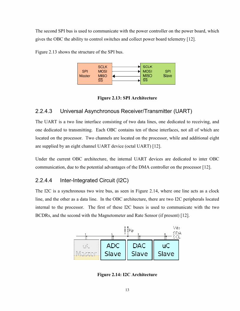
The second SPI bus is used to communicate with the power controller on the power board, which
gives the OBC the ability to control swi
Figure 2.13 shows the structure of the SPI bus.
2.2.4.3 Universal Asynchronous Receiver/Transmitter
The UART is a two line interface consisting of two da
one dedicated to transmitting
located on the processor. Two channels are located on the processor, while and additional eight
are supplied by an eight channel UART device (octal UART)
Under the current OBC architecture, the internal UART devices are dedicated to inter
communication, due to the potential
2.2.4.4 Inter-Integrated Circuit
The I2C is a synchronous two wire bus,
line, and the other as a data line.
internal to the processor. The first of these I2C bu
BCDRs, and the second with the
13
The second SPI bus is used to communicate with the power controller on the power board, which
gives the OBC the ability to control switches and collect power board telemetry
shows the structure of the SPI bus.
Figure 2.13: SPI Architecture
Universal Asynchronous Receiver/Transmitter (UART)
The UART is a two line interface consisting of two data lines, one dedicated to
o transmitting. Each OBC contains ten of these interfaces, not all of which are
located on the processor. Two channels are located on the processor, while and additional eight
ght channel UART device (octal UART) [12].
Under the current OBC architecture, the internal UART devices are dedicated to inter
due to the potential advantages of the DMA controller on the processor
Integrated Circuit (I2C)
The I2C is a synchronous two wire bus, as seen in Figure 2.14, where one line acts as a clock
e, and the other as a data line. In the OBC architecture, there are two I2C peripherals loc
sor. The first of these I2C buses is used to communicate with th
with the Magnetometer and Rate Sensor (if present)
Figure 2.14: I2C Architecture
The second SPI bus is used to communicate with the power controller on the power board, which
tches and collect power board telemetry [12].
(UART)
ta lines, one dedicated to receiving, and
. Each OBC contains ten of these interfaces, not all of which are
located on the processor. Two channels are located on the processor, while and additional eight
Under the current OBC architecture, the internal UART devices are dedicated to inter OBC
advantages of the DMA controller on the processor [12].
, where one line acts as a clock
In the OBC architecture, there are two I2C peripherals located
ses is used to communicate with the two
[12].

14
2.3 AISSat-1 Nanosatellite
The AISSat-1 mission, designated Automatic Identification System Satellite 1 (AISSat-1), is
being developed by SFL for the Norwegian government. AISSat-1 is a GNB derivative, whose
primary mission is to collect AIS data form ships in Norwegian waters. AIS is a ship based
tracking system, which has historically depended on line of site communications between ships
and stations along the shore. The primary goal of the AISSat-1 mission is to investigate the
feasibility of space based AIS monitoring of Norwegian waters. As a secondary mission,
AISSat-1 will use a triangulation scheme to determine ship locations based on received signal
strength. For this reason, GPS time synchronization must occur down to microsecond accuracy,
to ensure the best possible position information is known at the time an AIS packet is received.
The AISSat-1 mission patch can be seen in Figure 2.15.
Figure 2.15: AISSat-1 Mission Patch
2.3.1 AISSSat-1 Payload
To accommodate the AISSat-1 mission, the Generic Nanosatellite Bus will house an AIS Sensor.
Figure 2.16 shows the internal configuration of the GNB payload bay on AISSat-1.

15
Figure 2.16: AISSat-1 Payload Configuration [15]
2.3.1.1 AIS Sensor/Antenna
The AIS sensor is a Software Defined Radio (SDR) that will be used to receive AIS message
from maritime vessels. The SRD is a two channel VHF receiver and data processing unit used
for acquisition, decoding and forwarding of AIS messages. The two channel VHF receiver
operates at 161.975 and 162.025 MHz. The sensor will also help with various other tasks, like
basic signal environment investigation. This is accomplished by allowing the collection of signal
strength during time slots where no valid AIS messages are detected. It will also assist in ship
triangulation, through high accuracy time stamping of multiple AIS messages from each vessel.
A basic block diagram of the AIS sensor is shown in Figure 2.17 [4].
Figure 2.17: AIS Sensor Block Diagram [4]
In addition to the payload, AISSat-1 will contain a large VHF monopole antenna. Figure 2.18
shows AISSat-1 fully assembled, with the VHF monopole antenna in place.
Imped.match:Ant. to50 Ohm
LNA:50 Ohm,156.000-162.025MHz
A/D: FPGA: uC: I/F:RS-485
Microcontroller (uC)Software Defined Radio (SDR)
I/FConnector

16
Figure 2.18: AISSat-1 with VHF Monopole [15]
2.3.1.2 GPS Receiver
AISSat-1 will use an upgraded version of the GPS receiver flown on CanX-2. The main purpose
of the GPS will be to supply a PPS signal the POBC, which will be used to synchronize the
payload and satellite time.
2.3.1.3 Payload Computer
A standard GNB OBC will be dedicated to payload data handling, called the Payload On Board
Computer (POBC). The POBC will control the interface to the AIS Payload and GPS receiver.
For simplicity, the POBC is a feature reduced version of the standard GNB OBC design.

17
2.4 CanX-3 Nanosatellite
The CanX-3 mission, designated BRIght Target Explorer (BRITE), is a science mission designed
to observe brightness variations and temperature of some of the brightest stars in the sky.
BRITE will observe stars for up to 100 days at a time, allowing stellar variations on the order of
hours or months to be observed. There are currently four BRITE satellites in the works, with the
potential for two more coming on board in the near future. These four satellites are sectioned off
into two pairs that will form a constellation. Using these satellites as a constellation significantly
increases the observational duty cycle possible for a given star field. Each of the two pairs will
fly a different color filter, designed to observe different parts of the light spectrum. The
combined color data from both satellite pairs will allow astronomers to better identify modes of
oscillation, as unique data from different parts of the spectrum will be available. The BRITE
mission patch can be seen in Figure 2.19.
Figure 2.19: BRITE Mission Patch
2.4.1 CanX-3 Payload
To accommodate the BRITE mission, the Generic Nanosatellite Bus will house a telescope and a
star tracker in its payload bay. Figure 2.20 shows the internal configuration of the GNB payload
bay on BRITE.

18
Figure 2.20: BRITE Payload Configuration [14]
2.4.1.1 Telescope
The BRITE telescope is made up of an 11 megapixel CCD imager combined with custom optics.
These optics are designed to offer a 25 degree field of view, with the final star images slightly
defocused. Increased accuracy can be gained through slight defocusing of the stars point spread
function, as sharp spikes in intensity can increase the amount of under sampling error accrued.
A specially designed payload OBC will contain all supporting electronics. This OBC is
comprised of a standard GNB OBC, with all supporting CCD hardware on a single board. It will
read images from the CCD, perform any necessary processing, and store the final image into the
external FLASH on the OBC [14].
2.4.1.2 Star Tracker
An Aero-Astro star tracker is used to provide the arc-minute attitude determination required for
the BRITE mission. The star tracker is capable of 10deg/s tracking at 1 Hz, with a 3 second lost-
in-space solution acquisition time.

19
2.5 Canx-4 and CanX-5 Nanosatellites
CanX-4 and Canx-5, also denoted CanX-4&5, is a nanosatellite mission designed to demonstrate
on orbit formation flying. These satellites will autonomously achieve and maintain two different
formation flying patterns. The first is an along track orbit (ATO) formation, where one satellite
leads the other in the orbit by 500m and 1000m. The second is a projected circular orbit (PCO)
formation, where one satellite will appear to orbit the second, performed at 50m and 100m.
While both satellites are identical, with either of them capable of thrust maneuvers, only one
satellite will be actively maintaining the formation at any given time. This mission utilizes
carrier phase differential GPS to determine satellite relative positioning down to 10 cm
accuracies. With this position information, a formation flying algorithm using a cold gas
propulsion system will maintain formation flying to sub-meter accuracies. The CanX-4&5
mission patch can be seen in Figure 2.21 [14].
Figure 2.21: CanX-4 and CanX-5 Mission Patch
2.5.1 CanX-4 and CanX-5 Payload
To accommodate the CanX-4&5 mission, the Generic Nanosatellite Bus contain a propulsion
system, GPS receiver, intersatellite link, formation flying computer and an intersatellite
separation system. While all of these components are specific to the payload, not all are

20
contained within the payload bay. GNB was designed to contain flexible components like the
GPS receiver, which can be included in missions that require it. Figure 2.22 shows the internal
configuration of the payload bay for CanX-4&5.
Figure 2.22: CanX-4&5 Payload Configuration [14]
2.5.1.1 Propulsion System
The CanX-4&5 propulsion system, called the Canadian Advanced Nanosatellite Propulsion
System (CNAPS) was developed at SFL. This propulsion system consists of four nozzles, based
on the NANOPS propulsion system used successfully on CanX-2. The propellant used by
CNAPS is liquefied sulfur hexafluoride (SF6), which should allow CNAPS to achieve a specific
impulse of at least 35s. The total amount of fuel allotted to each satellite is 300cc, which gives
each satellite a maximum ∆V of 14 m/s [14].
2.5.1.2 GPS Receiver
CanX-4&5 will use an updated version of the GPS receiver used on CanX-2. The GPS receiver
will allow CanX-4 and CanX-5 to determine their absolute position and velocity to within 2-5m
(RMS) and 5-10cm/s (RMS) respectively. The University of Calgary has developed special
algorithms that use the absolute position and velocity of each satellite to calculate their relative
position and velocity to within 2-5 cm (RMS) and 1-3 cm/s (RMS) respectively. This highly
accurate relative position and velocity information is then passed to the formation flying
algorithm [14].

21
2.5.1.3 Intersatellite Link
The InterSatellite Link (ISL) is an S-Band transceiver that allows both satellites to communicate
directly with each other on orbit. The ISL can achieve data rates of up to 10 kb/s over a
maximum distance of 5 km [14].
2.5.1.4 Rate Gyros
In addition to the standard GNB attitude determination components, CanX-4&5 will also contain
a three axis rate gyro. The rate gyros will provide three-axis rate information to the ADCS, in
order to increase attitude determination accuracy during eclipse. The current rate gyro design
has a resolution of 0.05deg/s [14].
2.5.1.5 Intersatellite Separation System
After ejection from the launch vehicle, CanX-4 and CanX-5 will be attached to each other
through the Intersatellite Separation System (ISS). This is critical, as the satellites would drift
apart during the commissioning, ending the mission before it began. The ISS uses an electrically
de-bonding agent to hold the satellites together. During the separation sequence, a voltage is
applied across the glue, weakening it. Spring loaded plungers then cause the weakened bond to
break, and the satellites to separate with a pre-determined velocity. The initial velocity imparted
on the satellites was designed to place them in their first ATO obit with minimal control effort
[14].
2.5.1.6 Formation Flying Computer
A standard GNB OBC will be dedicated to the formation flying algorithm, called the Formation
Flying Computer (FFC). The FFC will control the interface to CNAPS, the GPS receiver, ISL
and ISS. Like in AISSat-1, FFC is a feature reduced version of the standard GNB OBC design.

3 GNB Software Architecture
The author was not directly involved in the development of this GNB software architecture, but
was responsible for implementing it through the development of the individual components seen
in Figure 3.1. All items show in blue, with exception of the SPI thread, was for the most part
designed and developed by the author. More detailed explanation of work
block can be found it their respective sections.
The GNB software architecture
ultimately lead to more robust and reliable application software
GNB application software such that any modification to hardware
affect a single application thread. In previous software designs multiple application threads
could access peripherals independently. A modification
to multiple threads, which can make updat
3.1 shows the high level architectural desi
software developed for the generic nanosatellite bus (GNB).
Figure
22
Software Architecture
The author was not directly involved in the development of this GNB software architecture, but
was responsible for implementing it through the development of the individual components seen
. All items show in blue, with exception of the SPI thread, was for the most part
designed and developed by the author. More detailed explanation of work
block can be found it their respective sections.
architecture was designed using the school of thought that modularity will
ultimately lead to more robust and reliable application software. There was a desire
software such that any modification to hardware or device driver
affect a single application thread. In previous software designs multiple application threads
could access peripherals independently. A modification to a driver would require modifications
to multiple threads, which can make updating software overly complex and error prone
shows the high level architectural design for the on-board computer (OBC)
developed for the generic nanosatellite bus (GNB).
Figure 3.1: GNB Software Architecture
The author was not directly involved in the development of this GNB software architecture, but
was responsible for implementing it through the development of the individual components seen
. All items show in blue, with exception of the SPI thread, was for the most part
designed and developed by the author. More detailed explanation of work completed on each
was designed using the school of thought that modularity will
. There was a desire to design the
or device driver would only
affect a single application thread. In previous software designs multiple application threads
r would require modifications
software overly complex and error prone. Figure
board computer (OBC) application

23
Under the current architecture, all application threads communicate with peripherals through
specially designed driver threads. These threads put an NSP front end on any device that does
not speak the protocol. Thus, a uniform NSP based communication system has been developed.
Application threads use the CANOE message handler to send NSP packets to the
communications thread. The communications thread then determines where to route the packets
based on the NSP destination address. CANOE is discussed in more detail in Section 3.1.
There are several disadvantages to the centralized driver control architecture, as opposed to
distributed control. These include loss of the single execution path peripheral access, and
message handling delay. While these issues make the design of application threads less
deterministic, the benefits of a modular design far outweigh the disadvantages. With careful
design, these effects can be mitigated.
3.1 Canadian Advanced Nanospace Operating Environment
The Canadian Advanced Nanospace Operating Environment (CANOE) was developed originally
by Cecilia Mok, as her masters work at SFL. The operating system was later ported to the GNB
platform by SFL engineer Nathan Gregory Orr, with some contribution made by the author.
CANOE is a real-time, mutli-threaded operating system providing basic functionality like
alarms, inter-thread messaging and system clocks [18].
A multi-threaded operating system allows for concurrent execution of multiple blocks of code
with a single execution path. These blocks of code are referred to as threads, with every thread
being task specific. CANOE uses constant length time slices, giving each thread an equal
amount of time to execute before moving on to the next (context switch). While threads are only
processed one at a time, the time slice is small enough that the execution of threads appears
simultaneous [18].
In addition to context switching CANOE supplies message handling features, allowing NSP
packets and event flags to be passed between application thread [18].

24
4 Software Requirements
All software requirements were pre-defined by project managers and directors at the Space
Flight Laboratory. The author used these pre-existing requirements in the design and
implementation of the spacecraft software, but made no contribution to the requirements defined
in the subsequent sections.
4.1 GNB OBC Software Requirements
Table 4-1 contains the software requirements for the Generic Nanosatellite Bus (GNB) Software
development, all organized by group [11].
No. Description Communication Requirements
1.1 A multithread capable OS will be utilized for conducting nominal spacecraft and experiment operations.
1.2 The OS shall be capable of sending transmissions using the S-band transmitter. (HKC ONLY) 1.3 The OS shall receive data and send commands from/to payloads. 1.4 The OS shall decode and encode NSP packets. 1.5 The OS shall encapsulate payload data in NSP packets. 1.6 The OS shall receive and respond to a ping command. 1.7 The OS shall only interpret and respond to transmissions that are addressed to it. 1.8 The OS shall include a satellite/station ID on all packets transmitted to the ground station.
1.9 The OS shall relay commands to/from the ground station to the ADCS/payload computers, according to the NSP protocol through their point-to-point serial links.
1.10 The OS should allow the transmission of messages between threads running on different computers using their point-to-point serial links.
Debugging Requirements 2.1 Commands shall be provided for debugging: peek and poke at memory locations.
Telemetry Requirements
3.1 The OS shall obtain telemetry from connected satellite systems when commanded to do so by the ground station.
3.2 The telemetry shall indicate the state of health of each major connected bus component and each connected payload.
3.3 The OS shall periodically obtain “WOD” telemetry and store it in a long term buffer (at least a days worth of data) for later retrieval.
Power Control Requirements
4.1 The OS shall support the querying of the state of all the power switches and allow the turning of switches on/off when commanded to do so by the ground station.
Memory, Software Loading and Execution Requirements
5.1 The core OS and applications should be able to be uploaded in one average length pass and shall be able to be uploaded in a maximum of two average length passes.
5.2 The OS shall store payload data in external Flash memory for later download. 5.3 The OS shall provide a file-system like abstraction layer for the external Flash memory.
5.4 The OS shall execute code at an address specified by ground command when commanded to do so by the ground.

25
5.5 OS shall allow safe termination of non-critical application threads. 5.6 The OS shall permit the starting or re-starting of non-critical application threads.
5.7 The OS shall permit the scheduling of hard real-time tasks to ensure the success of the ADCS algorithms.
OS Drivers for Subsystems and Payloads Requirements
6.1 The OS shall provide applications with access to power switching of connected subsystems and payloads.
6.2 The OS shall provide the applications with access to all telemetry sensors.
6.3 The OS shall provide applications with a concurrent multithread accessible driver for the 4-wire SPI busses.
6.4 The OS shall provide applications with a concurrent multithread accessible driver for the UART interfaces.
6.5 The OS shall provide applications with a concurrent multithread accessible driver for the I2C bus.
6.6 The OS shall provide applications with a driver for the SCC device.
6.7 OS will allow specific threads to place hard real-time requirements on their execution and on driver availability.
Attitude Control Sensors and Actuators Requirements
7.1 The operating system shall have support for receiving attitude information from six fine and six coarse sun sensors and the magnetometer.
7.2 The operating system shall have support for controlling attitude using three magnetorquer coils and three nano reaction wheels.
Formation Flying Hardware Requirements
8.1 The operating system shall have support for providing application software control of the spacecrafts GPS receiver.
8.2 The operating system shall have support for providing application software control of the spacecraft’s propulsion system.
8.3 The operating system shall have support for providing application software bi-directional communications with the other spacecraft through the ISL.
Scientific Payload Hardware Requirements
9.1 The operating system shall have support for providing application software communications with the spacecrafts telescope imaging computer and star tracking computer.
Table 4-1: GNB OBC Software Requirements [11]
4.2 AISSat-1 Payload Software Requirements
Table 4-2 contains the software requirements for the AISSat-1 Payload Software development,
all organized by group [1].
No. Description Communication Requirements
1.1 The application software shall receive data and send commands to/from the payload, other spacecraft computers, and the ground.
1.2 The application software shall decode and encode NSP packets according to the Nanosatellite Protocol (NSP) document [2].
1.3 The application software shall encapsulate payload data in a standard NSP packet. 1.4 The application software shall receive and respond to a ping command.

26
1.5 The application software shall only interpret and respond to transmissions that are addressed to it [3].
1.6 The application software shall include a satellite/station ID on all packets transmitted to the ground station [3].
1.7 The application software shall relay commands to/from the ground station to the payload, according to the NSP protocol through their point-to-point serial links.
1.8 The application software shall operate at a nominal baud rate of 57600 bps. Interface Requirements
2.1 The application software shall provide applications with a driver for the RS-232, RS-485 and TTL Serial interfaces.
2.2 The application software shall be capable of switching the payload on and off at the hardware level through commands to the HKC.
Debugging Requirements 3.1 Commands shall be provided for debugging: peek and poke at memory locations. Telemetry Requirements
4.1
The application software shall obtain telemetry from the payload computer and AIS sensor payload at a configurable rate (nominally 60 seconds) for storage and later download to the ground.
4.2 The application software shall provide the ground with access to all relevant telemetry. 4.3 The telemetry shall indicate the overall state of health of each major payload component. Memory, Software Loading and Execution
5.1 The application software should be able to be uploaded in one average length pass and shall be able to be uploaded in a maximum of two average length passes.
5.2 The application software shall store payload data in external Flash memory for later download.
5.3 The application software shall provide safeguards against damage to the boot strap sector of the internal FLASH memory.
5.4 The application software shall provide a file-system like abstraction layer for the external Flash memory.
5.5 The application software shall execute code at an address specified by ground command when commanded to.
5.6 The application software shall use flash in such a way that de-rated life cycle limits are not reached within the 3 year mission life time [4].
5.7 The application software shall have the capability to wash the external EDAC protected SRAM. 5.8 The application software should be able to run out of Internal Flash or External SRAM GPS Interface Requirements 6.1 The application software shall allow command and control of the spacecraft’s GPS receiver.
6.2 The application software shall be capable of cold starting the GPS device. It should be capable of assisting the start of the GPS through the upload of stored GPS ephemeris data.
6.3 The application software shall keep track of GPS lock state and store the lock state information with each payload data message.
6.4 The application software shall store position, velocity, and time from the GPS at a configurable rate (nominally every 60 seconds) when in a lock state [3].
Payload Operations Requirements
7.1 The application software shall be able to decode the bit stuffed AIS messages received from the payload.
7.2 The application software shall be able to distinguish AIS message types 1,2,3 & 4 [4]. 7.3 The application software shall be able to check the validity of the VDL (AIS) CRC [4].
7.4 The application software shall be capable of storing the first and last message of types 1-4 received from each ship in flash [4].

27
7.5
The application software shall be capable of sorting the messages stored in order of highest latitude, based on the last message stored. This can occur either at the time of reception or at the time of downlink [4].
7.6
During a contact window, the application software shall be capable of downlinking previously-stored AIS data while simultaneously either downlinking live AIS data or collecting and storing new AIS data. [4].
7.7 The application software shall be able to receive and process 4500 messages/minute [3]. 7.8 The application software shall be able to store messages from at least 20,000 vessels. Software Interface Requirements
8.1 The application software shall use the addresses defined in the Instrument Control Document to communicate with individual payload components.
8.2 The application software shall issue commands to and receive responses from the AIS sensor as defined in the Instrument Control Document [4].
8.3 The application software shall be able to process Single, Dual and empty time slot messages.
8.4 The application software shall be capable of transferring J2000 time within 2 PPS pulses to the payload to avoid second slip [3].
8.5 The application software shall be able to execute received commands as described in the AISSat-1 Payload Computer Software Design Document [5].
Table 4-2: AISSat-1 Payload Software Requirements
4.3 Time Tag Requirements
Table 4-3 below contains the software requirements for the Time Tag functionality for the GNB
Nanosatellite missions.
No. Description Time Tag Requirements
1.1 The spacecraft shall NACK commands that do not meet its expected format [7].
1.2
If the ground specifies upload must complete, the spacecraft shall be able to ensure that a group of commands is successfully uploaded, or none of the commands can execute in that group [7].
1.3 The spacecraft shall allow operators to manipulate the queue. Manipulations shall include flushing, editing, appending, reading and deleting arbitrary commands [7].
1.4 The spacecraft shall handle both relative and absolute times of execution [7].
1.5
The spacecraft shall supply the state of the onboard queue, including: number of active commands, number of empty slots and a time ordered sequence of current commands (as read back) [7].
Table 4-3: GNB Time Tag Requirements [6]

28
5 FLIGHT SOFTWARE
5.1 Validation of the AISSat-1 Payload OBC
Prior to the critical design review for the AISSat-1 nanosatellite mission, the Norwegian clients
requested that the on board computer (OBC) designed for the generic nanosatellite bus (GNB) be
tested and validated for that mission. The author, with support from Henry Spencer, was tasked
with developing the software for the AISSat-1 payload OBC using a prototype computer built by
Tarun Tully of the Space Flight Laboratory. Henry Spencer developed the payload software
architecture and the table storage code. The author was involved mainly in the implementation
for the architecture developed by Henry Spencer.
5.1.1 Software Architecture
CANOE, which is the operating system currently used on all GNB missions, allows multiple
applications to run concurrently on a single OBC. Early discussion of the payload computer
software architecture floated the idea of porting CANOE for use on the payload computer. If
CANOE were used, threads would be created to accomplish various tasks, like serial
communications and data processing. This approach was rejected due to a combination of
special requirements and the need to perform preliminary performance testing before CANOE
would be available.
The payload software architecture developed has four main functional blocks: the background
program (BP), the House Keeping Computer Driver (HKCD), the GPS Driver (GPSD) and the
Payload Driver (PD). Communications between each of the functional blocks is handled using
unidirectional links. All functional blocks, other then the Background Program, are interrupt
driven. This allows processing to occur when data is not being transmitted or received, but gives
priority to the receiver and transmitter when required. A graphical depiction of the payload
software architecture can be seen in Figure 5.1 [5].

29
Figure 5.1: Payload Software Architecture [5]
5.1.1.1 Background Program
The Background Program is responsible for all data handling and command processing for the
payload computer. Flow control on the links is accomplished through direct polling of each link
when the background program is in an idle state. When a link buffer is found to have a packet
set to SEND, it is processed in the manner appropriate to the link it is contained within. For
example, a packet in a link buffer from the HKCD to the BP link will be processed as a ground
command if its destination address matches the payload computer address. When the BP finds
that there is at least one packet in any of the transmit queues, it initiates a transfer by sending the
first byte over the serial port. After the first byte is sent, transmit interrupts carry out the
remainder of the data transmission.
All flash operations are processed by the background program. Polling stops during flash
operations, but interrupts are left enabled so that data can be received and currently active
transmissions can continue [5].
5.1.1.2 Drivers
The Drivers are implemented as a set of interrupt service routines (ISR). When a byte is sent
from one of the external devices to the payload computer, a receive interrupt is triggered. This
ISR then receives a byte and stores it in the currently active link buffer. When the character

30
received is the KISS framing character at the end of a received packet, the ISR sets an ownership
flag for the current link buffer to SEND. The next time the ISR is called, a new link buffer is
retrieved and the process repeats. No logical operations occur here, the only purpose of the
driver is to send and receive bytes based on the KISS framing characters. When a packet is sent
from the payload computer to another device, a transmit interrupt is triggered every time the
transmitter is available. The ISR increments a counter within the link structure when a byte is
transmitted, and clears the link after all bytes have been sent. This description covers the House
Keeping Computer Driver, Payload Driver and GPS Driver since they all work in an identical
manner [5].
5.1.1.3 Links
An individual link buffer is implemented as a structure that contains a data buffer and a number
of event flags and status variables. Due to the fact that the OBC cannot always deal with a sent
packet before another packet appears, each link is an array of link buffers (the number depending
on an analysis of worst-case backlogs). One link buffer in each link is reserved as a “garbage
buffer”, ignored by the receiver; if all normal link buffers of the link are full, new packets go into
the garbage buffer and hence are effectively discarded. This prevents buffer overflows that can
cause unpredictable software behavior [5].
5.1.1.4 Flash Storage
Due to the nature of the external flash, data to be stored is put into a special data structure. The
data structure consists of 2048 byte pages. There is some overhead produced by the page
structure, with additional overhead for each entry in the page. Each entry is preceded by two
bytes of framing characters. These two bytes consist of a flag byte and a byte containing the
number of bytes in the stored data. The flag byte keeps track of user defined variables like the
GPS lock state [5].
5.1.2 Data Handling
To simplify the payload computer software, it was decided that all incoming data would be
sorted and stored in FLASH. During data collection there will be no distinction between
operational modes as specified below:

31
OpsMode Observation GPS Storage VDL CRC Sorting Downlink 1 </=15% Yes Mode-1 No None All 2 </=15% Yes Mode-2 Yes Latitude First and Last 3 </=Full orbit No Mode-2 Yes None Last only 4 </=15% Yes None No None All
Table 5-1: AISSa-1 Operational Modes[4]
Every incoming packet with a valid NSP CRC is stored in FLASH, where it remains until that
region of flash is erased by ground command. To accommodate OpsModes 2 and 3, a table
structure is updated every time an Automatic Identification System (AIS) message of type 1-4 is
received. A graphical depiction of the data handling architecture can be found in Figure 5.2. [5].
Figure 5.2: Data Handling Architecture [5]
The only difference between operation modes is how the data is read out of memory, and
whether or not the received messages are passed directly to the ground. If mode 4 is requested, a
Feedthrough flag is set and received messages are passed to the ground, in addition to being
stored in FLASH. This approach prevents critical OpsMode 4 data from being lost during a
ground station dropout [5].
To accommodate OpsModes 2 and 3 downloading, a table structure was created to keep track of
the first and last messages for each ship. This structure consists of a large hash table using the
VDL CRC as its hashing function. Each element in the hash table acts as the head of a list of
ship structures. These structures keep pointers to the first and last message for each ship

32
observed, as well as their latitude. Table downloads will commonly occur during observations
periods, so two tables are running at any given time so that a new table can be started
instantaneously, when a table download is requested [5].
Using this approach, all operational mode requirements are satisfied as specified in the ICD [4].
The main difference is that in this mode all old data from any operational mode can be obtained
at any time until the section of FLASH it resides in is erased by ground command. This
approach, as shown in Figure 5.2, is achievable within the resources available. It has a
significant benefit in that it allows for maximum operational flexibility on the part of the
operator, as well as minimizing the loss of data due to ground outages or observation
interruptions [5].
5.1.3 Bit Stuffing
Messages received from the payload contain an “as is” AIS message with some extra information
appended to it. As such, the message itself is still in its original bit stuffed form. Before CRC
calculations can occur on the message, it must first be destuffed. Destuffing is straightforward,
using the standard SDLC algorithm, but understanding the proper bit ordering of the messages is
important. The following section describes the process required to destuff a message. The
process is not straight forward, and depends heavily on conventions that differ between computer
and communications engineers [5].
It is important to note that data saved into computer memory has been arranged in a logical
manner that is different from the bit stream coming in over the radio. Consider how bits received
on the radio are assembled into bytes for use by software. Suppose the radio order of some bits
is
...abcdefgh...
That is, bit "a" is sent first, "b" second, etc.
The usual old-style communications gear assembles bits into bytes lsb-first (that is, the first bit
received goes in the least-significant position in the byte):
…hgfedcba…

33
Once the data is restored to radio bit order, destuffing consists of simply scanning the data
between the start and end flags, looking for any sequence of five 1 bits followed by a 0 bit, and
deleting the 0 bit in all such cases [5].
5.1.4 Cyclic Redundancy Check
Early testing between Norway and UTIAS/SFL discovered inconsistencies in the AIS CRC
standards, mostly involving confusion between radio bit order and bit order within computer
bytes. Through careful testing, the inconsistency was resolved and successful CRC checking
implemented.
It was determined that the CRC of the received AIS messages could be calculated with some
minor post processing to the standard NSP CRC algorithm. To check the CRC of a received AIS
message, you must first destuff and delete the opening/closing framing flags (each a 01111110
bit pattern). You then calculate the standard NSP CRC on all but the last two bytes, and then
complement it. The final complement operation (equivalent to XOR with 0xffff) is common in
CRCs, but the standard NSP CRC doesn't do this. The last two bytes of the message are the
actual CRC value stored Least Significant Byte (LSB) first.
This algorithm can reproduce the CRC value in the "Fixed PRS data derived from ITU/T.0.153"
table, once it is understood that the bytes in that table are shown in radio order, which are not
LSB. Likewise, the CRC is quoted in radio bit order as well. Bit-reverse each byte in the table,
calculate the CRC as described in the previous paragraph, and bit-reverse that CRC value to get
the specified CRC in the table [5].
5.1.5 KISS Encoding
As defined by the NSP standard, all packets sent between devices are KISS encoded. KISS is a
framing protocol used for packet transmission across serial links. More detail can be found in
the Nanosatellite Protocol (NSP) v3 Specification document [2].
5.1.6 Test Results
Upon completion of the payload software, stress testing of the payload OBC was conducted
under worst case operational conditions. The author was responsible for setting up and running

34
the required payload functionality tests. This data was then parsed and presented to the
Norwegian clients during the AISSat-1 critical design review.
5.1.6.1 Test Setup
Figure 5.3: Set Up for the AISSat-1 Payload OBC Tests [5]
The AISSat-1 payload software was tested on a flight prototype OBC, derived from the standard
GNB design (Figure 5.3). To increase the test accuracy the OBC was operated at 10 MHz,
matching the speed of the external memory. External memory components had not been
populated when testing occurred, which forced a non-flight memory architecture to be used.
Since no external FLASH or SRAM was available, the internal flash and SRAM on the OBC
was used. This placed a limitation on the size of table that could be created for OpsMode 2 and
3 storage. This initial table size was set at 200 ships, which was only slightly larger than the test
set of data used by the payload simulator. Once the external memory is operational, the table
size will be set at approximately 30,000 ships [5].
In the following tests, the payload software was tested in each of the four operational modes, as
defined in the ICD [4]. The payload computer performed both data storage modes (bulk storage
of all raw AIS messages, and a filtered/sorted table of first and last messages). The only
distinguishable difference between operational modes is how operator chooses to download
payload data. All tests were performed with feedthough (OpsMode 4) active to capture the worst
case operating loads that will be seen on orbit [5].

35
5.1.6.2 Expected Performance Difference
The fully populated payload OBC will use external memory instead of the internal memory
architecture used in this test. The external memory will be clocked using a 10 MHz oscillator;
which limits the speed at which memory can be accessed. The on board memory used in the
initial testing did not have this limitation, which cannot be ignored [5].
The external FLASH is designed for faster write times than the internal flash, which is very slow.
Technical data from the manufactures data sheets show that the external flash can write a page
14 times faster on average. However, the external flash is slower at performing read commands
than the internal flash. Technical data from the manufacturer’s data sheets show that the internal
flash can read a page 9 times faster [5].
Since the external SRAM is speed limited, the best performance we can expect to see is 16 bit
accesses at 10 MHz. This is different than the internal SRAM architecture, which fetches 32 bits
at the system clock frequency (set at 10 MHz for the test). Thus the internal SRAM is 2 times
faster than the external SRAM [5].
The test software did not take advantage of the FIFO or DMA functionality available, and as
such there will be some performance advantages associated with them. These functions allow
the serial port to send or receive a pre-defined number of bytes before an interrupt occurs. This
will reduce the amount or processing time taken up by the receive and transmit interrupts. While
this will produce a significant increase in performance, it could not be quantified at the time and
was not be considered in the analysis [5].
In the analysis of Sections 5.1.6.3 to 5.1.6.6, CPU utilization values are calculated using timing
diagrams captured from actual test runs using a DigiView logic analyzer. Utilization values
were calculated for the actual test set up, along with projected utilization values based on the
performance increases and decreases of the separate components, as described above. This is
possible due to the fact that multiple logic probes were used to capture all possible processing
states, which to a large degree separates the FLASH and SRAM processes [5].

36
5.1.6.3 OpsMode 1
Testing of the payload computer, in combination with a payload simulator from FFI, showed
definitively that the GNB OBC design is capable of handling the real time processing
requirements of the AIS payload. For this test, the payload simulator was used to stream
simulated AIS data into the prototype OBC. For OpsMode 1, the payload data is only stored into
FLASH, with no sorting algorithms required. A timing diagram was created using a DigView
logic analyzer. GPIO pins were utilized by setting them high at the beginning of processing, and
low at the end. This timing diagram shows a snapshot of the CPU usage during an OpsMode 1
download in which data is continually streamed in through the simulator. Figure 5.4 shows the
timing of the various different processes [5].
Figure 5.4: OpsMode 1 Timing Diagram [5]
Initial inspection of Figure 5.4 can give the impression that the processor is saturated during
operation, but this is not the case. Figure 5.5 shows a close up view of Figure 5.4. It can be seen
at this resolution that a series of small pulses, caused by the interrupt service routines, meshes to
give the appearance of a solid bars in Figure 5.4 [5].
Figure 5.5: Close up of Figure 5.4 [5]
Using the timing diagrams, a Matlab function was created to analyze the raw data and produce
percent utilization values to characterize the performance. Percent utilization is defined as
shown below:
����������� ������ ������������
��������� ���� (5-1)

37
Analysis of the raw data in Figure 5.4 showed a percent utilization of 14%, which indicates that
the OBC was idle 86% of the time. This result satisfies requirements while keeping extensive
margin intact [5].
To better estimate actual percent utilization we expect when the external flash and SRAM are
installed, a secondary analysis was conducted on the raw data in Figure 5.4. This analysis
applied multiplication factors to each of the individual data lines. As an example, command
processing relies heavily on FLASH reads, so that line was multiplied by 9, which indicates that
it should take 9 times longer for commands to be processed. This is conservative because only a
fraction of this processing time is related to flash reads. Applying this analysis showed a worst
case percent utilization of 40%, which indicates that the OBC will still be idle 60% of the time.
This result shows that the GNB OBC design satisfies the mission requirements at peak load in
OpsMode 1 under worst case conditions [5].
5.1.6.4 OpsMode 2
This analysis was conducted identical to that of Section 5.1.6.3, with the only difference being
the operating state of the payload software. For this test, the payload simulator was used to
stream simulated AIS data into the prototype OBC. For OpsMode 2, the payload data is stored
into FLASH and AIS messages of type 1-4 are sorted into the ship table. In addition, payload
data was feed through directly to the ground. The timing diagram can be seen in Figure 5.6 [5].
Figure 5.6: OpsMode 2 Timing Diagram [5]
The test data produced a percent utilization of 23%, which indicates the OBC is idle 77% of the
time. Applying the multiplication factors produced an estimated utilization of 40%, with an idle
time of 60%. Thus the requirements are met in OpsMode 2 [5].

38
5.1.6.5 OpsMode 3
This analysis was conducted identical to that of Section 5.1.6.3, with the only difference being
the operating state of the payload software. For this test, the payload simulator was used to
stream simulated AIS data into the prototype OBC. For OpsMode 3, the payload data is stored
into FLASH and AIS messages of type 1-4 are sorted into the ship table. The only difference
between OpsMode 3 and OpsMode 2 is the downlinked packet size. OpsMode 3 contains only
the last message receive, while OpsMode 2 contains both the first and last. Additionionally,
payload data was feed through directly to the ground. The timing diagram can be seen in
Figure 5.7 [5].
Figure 5.7: OpsMode 3 Timing Diagram [5]
The test data produced a percent utilization of 19%, which indicates the OBC is idle 81% of the
time. Applying the multiplication factors produced an estimated utilization of 40%, with an idle
time of 60%. Thus the requirements are met in OpsMode 3 [5].
5.1.6.6 OpsMode 4
This analysis was conducted identical to that of Section 5.1.6.3, with the only difference being
the operating state of the payload software. For this test, the payload simulator was used to
stream simulated AIS data into the prototype OBC. For OpsMode 4, the payload data is feed
through directly to the ground. However, to capture the worst case conditions, data was stored
into FLASH, and the tables were updated. The timing diagram can be seen in Figure 5.8 [5].
Figure 5.8: OpsMode 4 Timing Diagram [5]

39
The test data produced a percent utilization of 19%, which indicates the OBC is idle 81% of the
time. Applying the multiplication factors produced an estimated utilization of 38%, with an idle
time of 62%. Thus the requirements are met in OpsMode 4 [5].
5.1.6.7 Conclusion
The results of Sections 5.1.6.3 to 5.1.6.6 are summarized in Table 5-2:
OpsMode Test (10 MHz) Idle Time (%)
Projected Flight (10 MHz) Idle Time (%)
1 86 60 2 77 60 3 81 60 4 81 62
Table 5-2: Payload Software Timing Results [5]
The analysis of sections 5.1.6.3 to 5.1.6.6 show that even under the most pessimistic assumptions
for the performance of the OBC, with external FLASH & SRAM installed, it still meets the
AISSat-1 mission requirements. Other performance boosting functions like the FIFOs and
DMAs will only increase the efficiency [5].
5.2 Driver Threads
The GNB software architecture required the development of several driver threads tasked with
enabling communication to external devices through peripherals on the OBC. The author has
been responsible for:
• Design & Implementation of the UART Thread;
• Design & Implementation of the SCC Thread;
• Design & Implementation of the I2C Thread;
• Implementing and NSP front end in the SPI Thread;
5.2.1 UART Thread
The UART Thread is responsible for communicating with external devices over the Universal
Asynchronous Receive/Transmit (UART) peripherals. As designed, there are ten unique serial
interfaces available for communication on the GNB OBC. These serial interfaces can be
separated into two distinct groups; the UART peripherals internal to the OBC processor, and the

UART expansion ports located on the OBC, but external to the processor
distinction between the two simple, they will
Octal UART (OUART) peripherals.
It is critical, due to the multi-
of receiving and transmitting
transmit buffer underflow and receive buffer overruns could o
5.2.1.1 Octal UART Architecture
To accommodate the real-
architecture for the octal UART peripherals
When an external device initiates communication
via 64 byte FIFO. When the FIFO
size, a receive interrupt is trigged for that
decoded on the fly, and placed in an
is received, this buffer is marked as a UART packet and sent to the communications thread
processing. Subsequent to the packet being sent to the communications thread, a new NSP
receive buffer is acquired and the process repeats.
When the OBC initiates a tra
transmit queue. The queue
40
UART expansion ports located on the OBC, but external to the processor
een the two simple, they will herein be referred to as the internal UART and
peripherals.
-threaded nature of CANOE, that the architecture derived
data while the thread is inactive. If this capability were
transmit buffer underflow and receive buffer overruns could occur.
Octal UART Architecture
-time requirements of the UART devices, the interrupt based
for the octal UART peripherals can be seen in Figure 5.9:
Figure 5.9: OUART Architecture
When an external device initiates communication, bytes are received by octal UART peripheral
FO. When the FIFO reaches a pre-set trigger level, nominally half of the FIFO
rrupt is trigged for that device. Data in the receive FIFO is clocked out, KISS
placed in an NSP receive buffer. When the final KIS
buffer is marked as a UART packet and sent to the communications thread
. Subsequent to the packet being sent to the communications thread, a new NSP
receive buffer is acquired and the process repeats.
hen the OBC initiates a transfer to an external device, pre-formed packets are placed in
allows the interrupt service routine to transmit clusters of packets
UART expansion ports located on the OBC, but external to the processor. To make the
ed to as the internal UART and
that the architecture derived be capable
his capability were not present,
time requirements of the UART devices, the interrupt based
octal UART peripheral
set trigger level, nominally half of the FIFO
device. Data in the receive FIFO is clocked out, KISS
KISS framing character
buffer is marked as a UART packet and sent to the communications thread for
. Subsequent to the packet being sent to the communications thread, a new NSP
formed packets are placed in a
allows the interrupt service routine to transmit clusters of packets

41
without intervention from the UART thread itself. To begin a transfer, bytes from the packet at
the end of the transmit queue, distinguished by the tail pointer, are KISS encoded on the fly into
the transmit FIFO of the desired octal UART peripheral. After several iterations, the complete
NSP packet has been transferred to the devices FIFO, and the packet is removed from the queue
and returned to the NSP list. This is accomplished by “popping” the last entry in the queue using
the tail pointer of the transmit queue structure.
Under the current architecture (with regards to the octal UART peripherals), the UART thread is
only responsible for correctly loading the transmit queues, initiating transfers when transmitters
are idle, diagnosing and recovering from failure states.
5.2.1.2 Internal UART Architecture
To accommodate the real-time requirements of the UART devices, the interrupt based
architecture for the internal UART peripherals can be seen in Figure 5.10 & Figure 5.11:
Figure 5.10: Internal UART Receive Architecture
Due to the lack of transmit and receive FIFOs, the Internal UART peripherals posed a significant
challenge architecturally. To counteract this deficiency, the on board direct memory access
(DMA) controller was used to create a simulated transmit and receive FIFO. A sequence of two
DMA control packets (used for commanding DMA sequences) were set up in an infinite loop.
Each packet directs the DMA controller to start processing the other at the end of a block
transfer. These packets direct the DMA controller to place all bytes received by the internal

UART peripherals into pre-defined buffers. When the block transfer completes (buffer is full),
an interrupt is trigged and the next control packet begins placing data in the second buffer.
in the DMA receive buffer is KISS decoded on the fly
was the case for the octal UART peripherals
packet to restore the daisy chain st
thread is responsible for checking the currently active DMA receive buffer for the remnants of
the last packet received, as the DMA
final KISS framing character is received, the NSP buffer is marked as a UART packet and sent
the communications thread for processing. Subsequent to the packet being sent to the
communications thread, a new NSP receive buffer is acquired
Under the current internal UART receive architecture, the UART thread is only r
polling the active DMA receive buffer for partial packets, and recovering from failure states.
Figure 5
Lack of a transmit FIFO on the internal UART pe
successfully transmit data. The device being communicated with, as per the NSP standard, will
simply wait until it receives a KISS framing character before processing the transmitted packet.
However, taking advantage of the on board direct memory access (DMA) controller will
significantly reduce the CPU utilization of the internal UART transmit functionality. Thus,
interrupt based DMA architec
functionality. This architecture can be seen in 42
defined buffers. When the block transfer completes (buffer is full),
an interrupt is trigged and the next control packet begins placing data in the second buffer.
ffer is KISS decoded on the fly and placed in an NSP receive buffer, as
for the octal UART peripherals. The interrupt service routine then resets the
packet to restore the daisy chain structure. Due to limitations of the DMA controller, the UART
checking the currently active DMA receive buffer for the remnants of
the last packet received, as the DMA controller does not have timeout functionality.
final KISS framing character is received, the NSP buffer is marked as a UART packet and sent
the communications thread for processing. Subsequent to the packet being sent to the
communications thread, a new NSP receive buffer is acquired and the process continues
Under the current internal UART receive architecture, the UART thread is only r
polling the active DMA receive buffer for partial packets, and recovering from failure states.
5.11: Internal UART Transmit Architecture
Lack of a transmit FIFO on the internal UART peripherals does not inhibit our ability to
successfully transmit data. The device being communicated with, as per the NSP standard, will
simply wait until it receives a KISS framing character before processing the transmitted packet.
tage of the on board direct memory access (DMA) controller will
significantly reduce the CPU utilization of the internal UART transmit functionality. Thus,
architecture was also developed for the internal UART transmit
This architecture can be seen in Figure 5.11.
defined buffers. When the block transfer completes (buffer is full),
an interrupt is trigged and the next control packet begins placing data in the second buffer. Data
ced in an NSP receive buffer, as
. The interrupt service routine then resets the control
ructure. Due to limitations of the DMA controller, the UART
checking the currently active DMA receive buffer for the remnants of
out functionality. When the
final KISS framing character is received, the NSP buffer is marked as a UART packet and sent to
the communications thread for processing. Subsequent to the packet being sent to the
and the process continues.
Under the current internal UART receive architecture, the UART thread is only responsible for
polling the active DMA receive buffer for partial packets, and recovering from failure states.
ripherals does not inhibit our ability to
successfully transmit data. The device being communicated with, as per the NSP standard, will
simply wait until it receives a KISS framing character before processing the transmitted packet.
tage of the on board direct memory access (DMA) controller will
significantly reduce the CPU utilization of the internal UART transmit functionality. Thus, an
ture was also developed for the internal UART transmit

43
When the OBC initiates a transfer to an external device, pre-formed packets are placed in a
transmit queue. The queue allows the interrupt service routine to transmit clusters of packets
without intervention from the UART thread itself. To begin a transfer, bytes from the packet at
the end of the transmit queue, distinguished by the tail pointer, are KISS encoded on the fly into
a DMA transmit buffer for the desired internal UART peripheral. A block transfer of the DMA
transmit buffer is then initiated. Once the block transfer completes, the DMA transmit buffer is
again filled, and the block transfer started once again. Once the complete NSP packet has been
transferred to the devices DMA transmit buffer, the packet is removed from the queue and
returned to the NSP list. This is accomplished by “popping” the last entry in the queue using the
tail pointer of the transmit queue structure.
Like the octal UART peripheral, the UART Thread is only responsible for loading the transmit
queue, initiating transfers when transmitters are idle, diagnosing and recovering from failure
states.
5.2.1.3 UART Thread Compatibility
The architecture described in Sections 5.2.1.1 & 5.2.1.2 are only a subset of the capabilities of
the UART Thread used to communicate with devices using the NSP protocol. In actual design
applications, not all devices will use this protocol, and as such it is important that the UART
thread be able to accept alternative architectures for specific peripherals.
To accommodate the possible need for alternative architectures, the UART Thread uses sets of
function pointers when executing ISRs, or polling of transmit or receive infrastructure. By
default, all pointers are set up to use the architecture described in Sections 5.2.1.1 & 5.2.1.2,
which is the nominal operating case. If a device requires a different protocol at its interface,
single functions can be created, and the function pointers initialized subsequently.
The UART Thread was also designed to be generic across all GNB missions. It can be used on
the ADCC, HKC and POBC of any mission, with only minor modifications to a single
configuration header file. This approach limits the amount of non-recurring engineering time
required to set up the flight software for the AISSat-1, BRITE and CanX 4/5 missions.

5.2.2 SCC Thread
The SCC thread is responsible for handling communications
SCC has only two channels, one dedicated to the UHF receiver, and the o
Band transmitter. To simplify things even further, only half duplex communication is required
for each channel. For these reasons, the SCC thread is the simplest thread written, with most of
its code ported from the CanX
some time. Figure 5.12 shows the high level architecture
data flow for both transmit and receive lines
When the UHF receiver detects valid HDLC framing characters
SCC peripheral via 32 byte FIFO
interrupt is trigged for that device. Data in the receive FIFO
receive buffer. Since the SCC uses the HDLC protocol, KISS encoding of that data is not
required. When the final HDLC framing character is complete, the NSP packet is marked as a
radio packet and sent to the communications thread
new NSP receive buffer is acquired and the process repeats.
When the OBC initiates a transfer
transmit queue. The queue allows the interrupt service routine to transmit clusters of packets
without intervention from the
end of the transmit queue are 44
is responsible for handling communications over the external SCC device. The
SCC has only two channels, one dedicated to the UHF receiver, and the other dedicated to the S
ansmitter. To simplify things even further, only half duplex communication is required
for each channel. For these reasons, the SCC thread is the simplest thread written, with most of
its code ported from the CanX-2 flight software, which has been used successfully in space for
shows the high level architecture design of the SCC thread
both transmit and receive lines.
Figure 5.12: SCC Architecture
detects valid HDLC framing characters, data bytes are
byte FIFO. When the FIFO reaches a pre-set trigger level
interrupt is trigged for that device. Data in the receive FIFO is clocked out and placed in an NSP
Since the SCC uses the HDLC protocol, KISS encoding of that data is not
HDLC framing character is complete, the NSP packet is marked as a
radio packet and sent to the communications thread. Subsequent to the packet being
new NSP receive buffer is acquired and the process repeats.
When the OBC initiates a transfer to the S-Band transmitter, pre-formed packets are placed in a
transmit queue. The queue allows the interrupt service routine to transmit clusters of packets
without intervention from the SCC thread itself. To begin a transfer, bytes from the packet at t
are copied into the transmit FIFO of the desired SCC
over the external SCC device. The
ther dedicated to the S-
ansmitter. To simplify things even further, only half duplex communication is required
for each channel. For these reasons, the SCC thread is the simplest thread written, with most of
software, which has been used successfully in space for
of the SCC thread, including
bytes are captured by the
set trigger level, a receive
and placed in an NSP
Since the SCC uses the HDLC protocol, KISS encoding of that data is not
HDLC framing character is complete, the NSP packet is marked as a
. Subsequent to the packet being shipped, a
formed packets are placed in a
transmit queue. The queue allows the interrupt service routine to transmit clusters of packets
thread itself. To begin a transfer, bytes from the packet at the
SCC peripheral. After

several iterations, the complete NSP packet has been transferred to the devices FIFO, and the
packet is removed from the queue
The main purpose of the SCC thread is to start transmissions when the queue is idle, and discard
packets if the S-Band transmitter
5.2.3 I2C Thread
The complexities of operating the I2C peripheral
developed. This architecture is based around the concept that the I2C threa
front end on all devices communicated with. Most devices connected to the on
through an I2C bus speak NSP, but s
for the I2C thread.
When an NSP packet is received from the communica
queue. Once the I2C device is available, a packet is popped out of the queue and passed into a
packet processing routine. This routine, based on the destination address and command bit,
determines which mode the I2C peripheral should
If a packet is destined for an NSP device, it is
initiates a transfer to the device, expecting an immediate reply. This is discussed in more detail
in Section 5.2.3.1.
45
several iterations, the complete NSP packet has been transferred to the devices FIFO, and the
packet is removed from the queue and returned to the NSP list.
The main purpose of the SCC thread is to start transmissions when the queue is idle, and discard
Band transmitter is disabled.
ating the I2C peripheral require a rather uni
This architecture is based around the concept that the I2C threa
ces communicated with. Most devices connected to the on
through an I2C bus speak NSP, but some do not. Figure 5.13 shows the high level architecture
Figure 5.13: I2C Architecture
When an NSP packet is received from the communications thread, it is placed in an NSP packet
e. Once the I2C device is available, a packet is popped out of the queue and passed into a
packet processing routine. This routine, based on the destination address and command bit,
e I2C peripheral should operate in for that interaction.
is destined for an NSP device, it is passed into an I2C NSP routine. This
initiates a transfer to the device, expecting an immediate reply. This is discussed in more detail
several iterations, the complete NSP packet has been transferred to the devices FIFO, and the
The main purpose of the SCC thread is to start transmissions when the queue is idle, and discard
require a rather unique architecture be
This architecture is based around the concept that the I2C thread is placing an NSP
ces communicated with. Most devices connected to the on-board computer
shows the high level architecture
tions thread, it is placed in an NSP packet
e. Once the I2C device is available, a packet is popped out of the queue and passed into a
packet processing routine. This routine, based on the destination address and command bit,
operate in for that interaction.
passed into an I2C NSP routine. This routine
initiates a transfer to the device, expecting an immediate reply. This is discussed in more detail

If a packet is destined for a non
passed into the I2C READ routine.
data transmission. This is discussed in more detail in
Finally, if a packet is destined for a non
I2C_WRITE, it is passed into the I2C WRITE routine. This routine initiates a write to the
device, without expecting a reply.
5.2.3.1 I2C NSP
When the I2C thread receives a packet that is destined for an NSP device, the I2C NSP routine is
called. The routine then initiates a transfer, with the I2C device set up in master transmit
with no stop condition. After being
transfer. Once all bytes in the NSP buffer have b
to master receive mode. The receive ISR then t
KISS framing character is detected
the communications thread, and the I2C bus released for
the BCDR and Rate Gyro are both designed to speak NSP over the I2C bus. Hence, these
devices require the I2C NSP architecture.
architecture.
46
If a packet is destined for a non-NPS device, and the command of the packet is I2C_READ
routine. This routine initiates a read from the device, without any
data transmission. This is discussed in more detail in Section 5.2.3.2.
Finally, if a packet is destined for a non-NSP device, and the command of the packet is
I2C_WRITE, it is passed into the I2C WRITE routine. This routine initiates a write to the
device, without expecting a reply. This is discussed in more detail in Section
When the I2C thread receives a packet that is destined for an NSP device, the I2C NSP routine is
called. The routine then initiates a transfer, with the I2C device set up in master transmit
After being initiated by the routine, the transmit ISR takes over the
Once all bytes in the NSP buffer have been transmitted, the I2C device
mode. The receive ISR then takes over, collecting all bytes received until a
detected. The NSP buffer is then marked as an I2C packet and sent to
, and the I2C bus released for the next queued up packet. Currently,
the BCDR and Rate Gyro are both designed to speak NSP over the I2C bus. Hence, these
devices require the I2C NSP architecture. Figure 5.14 shows the high level I2C NSP
Figure 5.14: I2C NSP Architecture
NPS device, and the command of the packet is I2C_READ, it is
itiates a read from the device, without any
device, and the command of the packet is
I2C_WRITE, it is passed into the I2C WRITE routine. This routine initiates a write to the
5.2.3.3.
When the I2C thread receives a packet that is destined for an NSP device, the I2C NSP routine is
called. The routine then initiates a transfer, with the I2C device set up in master transmit mode,
transmit ISR takes over the
een transmitted, the I2C device is re-configured
all bytes received until a
marked as an I2C packet and sent to
next queued up packet. Currently,
the BCDR and Rate Gyro are both designed to speak NSP over the I2C bus. Hence, these
shows the high level I2C NSP

5.2.3.2 I2C Read
When the I2C thread receives a packet that
command, the I2C READ routine is called. The routine then initiates a transfer, with the I2C
device set up in master receive
initiated by the routine, the receive
field of the received NSP packet until th
returned to the sender as an acknowledge
then released, allowing the next queued up packet to be p
level I2C read architecture.
5.2.3.3 I2C Write
When the I2C thread receives a packet that is destined for a non
command, the I2C WRITE routine is called. The routine then initiates a transfer, with the I2C
device set up in master transmit mode with
initiated by the routine, the transmit ISR takes over the transfer.
the sender as an acknowledgement to their I2C_
allowing the next queued up packet to b
architecture.
47
When the I2C thread receives a packet that is destined for a non-NSP device
routine is called. The routine then initiates a transfer, with the I2C
receive mode with data length and stop condition set
receive ISR takes over the transfer. Data bytes are
received NSP packet until the last byte has been received. The packet is then
returned to the sender as an acknowledgement to their I2C_READ command. The I2C bus is
then released, allowing the next queued up packet to be processed. Figure
Figure 5.15: I2C Read Architecture
When the I2C thread receives a packet that is destined for a non-NSP device with an I2C
routine is called. The routine then initiates a transfer, with the I2C
transmit mode with data length and stop condition set. After being
transmit ISR takes over the transfer. The packet is then returned to
the sender as an acknowledgement to their I2C_WRITE command. The I2C bus is then released,
allowing the next queued up packet to be processed. Figure 5.16 shows the high level I2C
NSP device with an I2C read
routine is called. The routine then initiates a transfer, with the I2C
data length and stop condition set. After being
fer. Data bytes are stored in the data
e last byte has been received. The packet is then
to their I2C_READ command. The I2C bus is
Figure 5.15 shows the high
NSP device with an I2C write
routine is called. The routine then initiates a transfer, with the I2C
dition set. After being
The packet is then returned to
command. The I2C bus is then released,
shows the high level I2C write
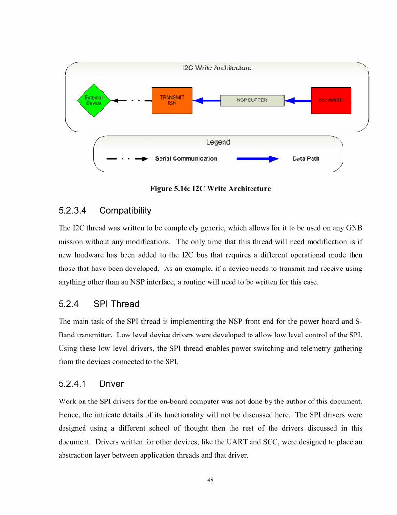
5.2.3.4 Compatibility
The I2C thread was written to be completely generic, which allows for it to be used on any GNB
mission without any modifications
new hardware has been added to the I2C bus that req
those that have been developed. As an example, if a device needs to transmit and receive
anything other than an NSP interface, a routine will need to be written for this case.
5.2.4 SPI Thread
The main task of the SPI thread is implementing the NSP front end for the power board and S
Band transmitter. Low level device drivers were developed to allow low level control of the SPI.
Using these low level drivers, the SPI thread enables power switching and telemetry gat
from the devices connected to the SPI.
5.2.4.1 Driver
Work on the SPI drivers for the on
Hence, the intricate details of its functionality will not be discussed her
designed using a different school of thought th
document. Drivers written for other devices, like the UART and SCC, were designed to place an
abstraction layer between application threads and that drive
48
Figure 5.16: I2C Write Architecture
Compatibility
The I2C thread was written to be completely generic, which allows for it to be used on any GNB
mission without any modifications. The only time that this thread will need modification is if
new hardware has been added to the I2C bus that requires a different operational mode then
those that have been developed. As an example, if a device needs to transmit and receive
anything other than an NSP interface, a routine will need to be written for this case.
PI thread is implementing the NSP front end for the power board and S
. Low level device drivers were developed to allow low level control of the SPI.
Using these low level drivers, the SPI thread enables power switching and telemetry gat
from the devices connected to the SPI.
Work on the SPI drivers for the on-board computer was not done by the author of this document.
the intricate details of its functionality will not be discussed here. The SPI drivers were
d using a different school of thought then the rest of the drivers discussed in this
document. Drivers written for other devices, like the UART and SCC, were designed to place an
abstraction layer between application threads and that driver.
The I2C thread was written to be completely generic, which allows for it to be used on any GNB
. The only time that this thread will need modification is if
uires a different operational mode then
those that have been developed. As an example, if a device needs to transmit and receive using
anything other than an NSP interface, a routine will need to be written for this case.
PI thread is implementing the NSP front end for the power board and S-
. Low level device drivers were developed to allow low level control of the SPI.
Using these low level drivers, the SPI thread enables power switching and telemetry gathering
board computer was not done by the author of this document.
e. The SPI drivers were
n the rest of the drivers discussed in this
document. Drivers written for other devices, like the UART and SCC, were designed to place an

49
The SPI driver was written to be a basic, generic interface between any software and the SPI
devices. Reading and writing can, at most, be done a half word at a time. Implementing the
driver in this way makes the code more portable, but requires the SPI thread to supply the front
end for any device on the SPI bus.
The SPI thread, written in part by the author, implements the required front end for the Power
Board and S-Band transmitter.
5.2.4.2 Power Board Front End
The SPI thread adds NSP front end functionality for communication with the power controller.
A special sequence of commands to the power controller is required to execute various tasks.
Forcing other application threads to run these sequences is inefficient, and would increase code
size significantly. Instead, the SPI thread allows operators or application threads to collect
telemetry, toggle switches, modify torquer current and initiate a power controller rest. All of this
functionality is possible through simple NSP commands sent to the power board. From the
perspective of any other application thread, it would appear that the power board itself was an
NSP device.
5.2.4.3 S-Band Transmitter Front End
The SPI thread adds NSP front end functionality for communications with the Analoge to Digital
Converter (ADC) on the S-Band transmitter. The ADC values contain S-Band telemetry used to
track the health of the transmitter. A special sequence of commands sent over the SPI is required
to successfully communicate with the ADC. Forcing other application threads to run these
sequences is inefficient, and would increase code size overall. Instead, the SPI thread allows
operators and application threads to collect the ADC values through a standard NSP telemetry
command. From the prospective of any other application thread, it would appear that the S-Band
transmitter is an NSP device.
5.3 Communications Thread
The communications thread was initially developed by Nathan Orr of the Space Flight
Laboratory. The author was responsible for completing its implementation through the addition
of S-Band transmitter control and a set of standard NSP commands.

The communications thread
GNB OBC. All application th
communications architecture.
by using the NSP destination address of received messages to rout
Figure 5.17 shows the architectural design of the communications thread.
Figure
When an NSP packet is received from any application thread, via the CANOE message handling,
it is first passed into a message va
through CRC and sanity checks. Once the packet
message routing routine. The packet is then sent
correct thread, based on its NSP destination address. If it
thread, it is processed as a command.
packets between multiple computers. The routing table
destined for another device to the proper drive
In addition to packet forward
Transmitter through a TxSelect
50
is one of the most critical parts of the software architecture on the
ion threads are designed around the premise that there is a centralized
communications architecture. The communications thread creates this centralized architecture
by using the NSP destination address of received messages to route them to the correct thread.
shows the architectural design of the communications thread.
Figure 5.17: Communications Thread Architecture
When an NSP packet is received from any application thread, via the CANOE message handling,
it is first passed into a message validation routine. Based on the packet type, it is validated
sanity checks. Once the packet has been deemed valid, it is passed
. The packet is then sent through the CANOE message handling
correct thread, based on its NSP destination address. If it is addressed to the communications
as a command. This centralized architecture allows for easy forwarding of
packets between multiple computers. The routing table directs any packets with NSP addresses
destined for another device to the proper driver thread.
In addition to packet forwarding, the communications thread also con
TxSelect command. This command is described in more detail in
is one of the most critical parts of the software architecture on the
are designed around the premise that there is a centralized
The communications thread creates this centralized architecture
to the correct thread.
When an NSP packet is received from any application thread, via the CANOE message handling,
ased on the packet type, it is validated
has been deemed valid, it is passed on to a
through the CANOE message handling to the
addressed to the communications
This centralized architecture allows for easy forwarding of
any packets with NSP addresses
also controls the S-Band
This command is described in more detail in Section

51
5.3.1.1. When commanded to turn on the S-Band transmitter, the proper control lines are set
turning the transmitter on. The SPI and SCC lines are then taken out of their tristate mode. The
transmitter is turned off and the SPI & SCC peripherals are put back into their tristate mode
when one of the following conditions occur. Either the satellite is sent a TxSelect command to
use anything other then the S-Band transmitter, or an S-Band timeout occurs. By design, the S-
Band transmitter cannot be active for more than a pre-determined period of time.
The SPI lines and the SCC transmit lines are tristated so that neither computer interferes with the
others ability to communicate with the S- Band transmitter. This is a direct result of the
redundant OBC architecture. These lines are shared by both computers, but are not designed to
be mult-mastered.
5.3.1 Commands
In addition to the message routing functionality, the communications thread also implements the
TxSelect, Ping and Init commands.
5.3.1.1 TxSelect Command
The TxSelect command allows the operator to set the path data must use to reach the ground
station. If the satellite is TxSelected to SBAND, packets destined for the ground will be
transmitted through the S-Band transmitter. During testing, operators can TxSelect the
spacecraft to testport, which would direct the satellite to send ground packets over the testport.
Upon startup, the TxSelect flag is set to “none”, which will direct the satellite the discard any
packets destined for the ground. The satellite will only respond once it has been TxSelected into
a valid state.
5.3.1.2 Ping Command
The Ping command allows the operator to test that the satellite is responsive, and to determine
which instance of software is running. Application code is designed to listen for ping commands
sent to the communications thread and bootloader. This single uniform ping command allows
the ground to indentify whether or not the OBC is in application mode or bootloader.

52
5.3.1.3 Init Command
The Init command allows the operator to either reset the OBC, or branch to pre-position code.
The main function of the init command is to drop out of application mode to bootloader. When
an init to zero is requested, a software reset is triggered. When an init to anything but zero is
requested, the code at that address is executed. Once the code is finished executing, it will return
and the application code will begin running once again.
5.3.2 Compatibility
The communications thread was designed to be highly compatible across the entire spectrum of
GNB missions. When moving between satellites, all that needs to be modified is the routing
table.
5.4 Power Thread
The power thread has been designed to handle all power related tasks on the GNB on board
computer (OBC). These tasks include software overcurrent protection and power switch control.
The power thread was conceived, designed and implemented by the author in response to the
need to have distributed switch control on the satellite.
Various application threads, like the ACS thread on the ADCC, need to actively turn switches on
and off during normal operation. As such, it is inefficient to have switch control occur on a
distributed basis. The power thread supplies a centralized power control architecture, where any
application thread can control the switch state, and duration of switch activations by sending
simple power commands. Switch control is discussed in more detail in Section 5.4.2.
The software overcurrent protection is designed to complement the hardware overcurrent
protection, adding an extra layer of protection against overcurrent events. The power thread
implements two main overcurrent protection schemes. The first is a peak current scheme, and
the second is an average power based scheme. Overcurrent protection is discussed in more detail
in Section 5.4.1.

53
5.4.1 Overcurrent Protection
There are two distinct forms of software overcurrent protection built into the power thread. The
first is peak current cutoff protection, where the absolute current measured is the deciding factor.
The second is average power cutoff, where the average power consumed decides when an
overcurrent event should be triggered.
5.4.1.1 Peak Current Cutoff
The power switches, located on the power board, have built in hardware overcurrent limits. It is
desired to set lower software overcurrent limits to help reduce the potential damage an
overcurrent event may case on any given device. This simple case is accommodated by reading
current values for each switch from the analogue to digital converters (ADCs) on the power
board. If a current exceeds a pre-set limit for two or more subsequent readings, an overcurrent
event is triggered, the switch is turned off, and an overcurrent event is stored in WOD. After the
overcurrent event has occurred, control of the switch will be disabling until operator
intervention. It is important to prevent automated systems, like the ACS, from turning the device
back on after an overcurrent event has occurred [10].
5.4.1.2 Average Power Cutoff
Due to single event effects, there is a distinct possibility that an event could cause a device to
consume more current than expected without triggering a peak current cutoff event. As such, it
is important that the overcurrent protection system be able to track the mean power consumption
of the device, and trigger an overcurrent event should this mean power rise above a pre-set limit.
In analog electronics, mean power consumption can be monitored through the use of a properly
designed low pass filter circuit. A software based low pass filter design was chose as a means of
tracking the average power consumption of various devices on the satellite. Figure 5.18 shows
an electrical low pass filter design, which is an electrical analogue to the desired software based
low pass filter. By solving for this circuit in the time domain, and then discretizing the solution,
we can create a software based low-pass filter for use in the overcurrent protection system [9].

Figure
From Kirchoffs Laws, and the definition of capacitance, the following equations are required to
represent the system in Figure
These three equations, once manipulated, simplify to the equation below
Now discretizing, with time step
Finally, after some re-arranging
Equation 4-7 is now it a state where
the units for both of these values are identical, we have a non
following equation is equally valid:
54
Figure 5.18: Electrical Low Pass Filter [9]
From Kirchoffs Laws, and the definition of capacitance, the following equations are required to
Figure 5.18 [9]:
These three equations, once manipulated, simplify to the equation below [9]:
, with time step , the system becomes [9]
arranging, we obtain a software based low-pass filter [9]
state where the only variable terms are and
the units for both of these values are identical, we have a non-dimensional equation
following equation is equally valid:
From Kirchoffs Laws, and the definition of capacitance, the following equations are required to
(5-2)
(5-3)
(5-4)
(5-5)
(5-6)
[9]:
(5-7)
and . Since
dimensional equation. Hence, the
(5-8)

The constant will be determined through
is not required.
This software based low-pass filter was implemented using current and voltag
collected from the Analogue
mean power from the filter exceeds a pre
event stored in WOD. The offending switch
intervenes. It is important to prevent automated systems, like the ACS, from turning the device
back on after an overcurrent event has occurred.
To test the robustness of the low
the equation 4-8. The value of
amount of phase lag in the system.
generated noise levels mask the power ramp that occurs when the time reaches 300 seconds.
Figure
Unseen in Figure 5.19, but present in
lines (black dashed), and the mean power cutoff lines (red dashed).
power values referenced here are the product of raw ADC values, and do not represent actual
power numbers. With a mean power cutoff set at 2.5
overcurrent event even under normal operations.
55
will be determined through testing; an exact theoretical definition of this constant
pass filter was implemented using current and voltag
collected from the Analogue to Digital Converters (ADCs) on the power board
from the filter exceeds a pre-set limit, the switch is turned off
event stored in WOD. The offending switch cannot be turned back on
. It is important to prevent automated systems, like the ACS, from turning the device
back on after an overcurrent event has occurred.
To test the robustness of the low-pass filter approach, a MATLAB simulation was written using
alue of was chosen to give the fastest response time, with the least
amount of phase lag in the system. Figure 5.19 shows the unfiltered case, where large
generated noise levels mask the power ramp that occurs when the time reaches 300 seconds.
Figure 5.19: Unfiltered Power Ramp Case
, but present in Figure 5.20 & Figure 5.21 are the mean power production
lines (black dashed), and the mean power cutoff lines (red dashed). It is important to note that
power values referenced here are the product of raw ADC values, and do not represent actual
an power cutoff set at 2.5x10⁶, the unfiltered case would trigger this
nt even under normal operations. Figure 5.20 shows the effect of a single low
an exact theoretical definition of this constant
pass filter was implemented using current and voltage telemetry
on the power board. When the output
set limit, the switch is turned off and an overcurrent
cannot be turned back on until an operator
. It is important to prevent automated systems, like the ACS, from turning the device
ss filter approach, a MATLAB simulation was written using
was chosen to give the fastest response time, with the least
case, where large randomly
generated noise levels mask the power ramp that occurs when the time reaches 300 seconds.
are the mean power production
It is important to note that all
power values referenced here are the product of raw ADC values, and do not represent actual
, the unfiltered case would trigger this
ffect of a single low

pass filter being applied to the unfiltered data. The output data has some jitter associated with it,
but this jitter is only a tiny percentage of what was observed in the unfiltered case.
Figure 5.20
Increasing the beyond that used in
but also increases the phase lag considerably. In order to clean the signal up further, a series of
software based low-pass filters
The resultant smoothing in Figure
low pass filters together, which resulted
90 seconds.
Figure 5.2156
pass filter being applied to the unfiltered data. The output data has some jitter associated with it,
but this jitter is only a tiny percentage of what was observed in the unfiltered case.
20: Single Low-Pass Filter applied to Figure 5.
beyond that used in Figure 5.20 does increase the smoothing effect of the filter,
but also increases the phase lag considerably. In order to clean the signal up further, a series of
pass filters were cascaded.
Figure 5.21 was acquired by cascading three separate software base
low pass filters together, which resulted in an incredibly stable output, with
21: Three Low-Pass Filters applied to Figure 5.
pass filter being applied to the unfiltered data. The output data has some jitter associated with it,
but this jitter is only a tiny percentage of what was observed in the unfiltered case.
.19
does increase the smoothing effect of the filter,
but also increases the phase lag considerably. In order to clean the signal up further, a series of
was acquired by cascading three separate software base
a phase lag of about
.19

57
The level of smoothing, and the acceptable phase lag are determined on a per-device basis.
Further testing on final flight hardware is required to finalize these values, and will be completed
at a future date.
5.4.2 Switch Control
Owing to the redundant OBC architecture used on the GNB missions, power switching is not
deterministic if tight regulations are not placed on switch control. The power board determines
the state of individual switches by XORing the desired value from both OBCs. If the HKC turns
on a switch, the ADCC would have to invert its logic to turn it back off. The implication is that
now the ADCC has to turn the switch “ON” to get it to turn off [10].
To avoid the XORing factor, and maintain deterministic control of power switches, the ADCC
and HKC have been assigned specific switches that only they can control in Table 5-3. SPI Address
SA[4:0] Switch/Command Default
State Nominally
Commanded By
0 Beacon Disable Engage OFF HKC
1 Magnetometer OFF ADCC
2 All Sun Sensors (See Note 1) OFF ADCC
3 +X Fine Sun Sensor OFF ADCC
4 -X Fine Sun Sensor OFF ADCC
5 +Y Fine Sun Sensor OFF ADCC
6 -Y Fine Sun Sensor OFF ADCC
7 +Z Fine Sun Sensor OFF ADCC
8 -Z Fine Sun Sensor OFF ADCC
9 X Wheel OFF ADCC
10 Y Wheel OFF ADCC
11 Z Wheel OFF ADCC
12 Rate Gyro / Spare OFF ADCC
13 X Magnetorquer OFF ADCC
14 Y Magnetorquer OFF ADCC
15 Z Magnetorquer OFF ADCC
16 X Magnetorquer Direction Low ADCC
17 Y Magnetorquer Direction Low ADCC
18 Z Magnetorquer Direction Low ADCC
19 GPS/Star Tracker OFF ADCC
20 GOC / Spare OFF HKC
21 Payload OFF HKC

58
22 Spare OFF HKC
23 Beacon ON HKC
24 Beacon Disable Enable OFF HKC
25 Loadshed Latch Reset OFF HKC
26 BCDR 0 (See Note 2) OFF HKC
27 BCDR 1 (See Note 2) ON HKC
28 Star Tracker Reset / GPO Low ADCC
29 GPIO0 (See Note 3) Low HKC
30 GPIO1 (See Note 3) Low HKC
31 GPIO I/O Select (See Note 3 and
4) Input HKC
Table 5-3: Switch Control Designation [10]
Any attempt by an OBC to control a switch that is not assigned to it will result in the command
being returned with the acknowledge bet set to zero (NACK).
5.4.2.1 Switch Control Bypass
In the case that an operator must control switches which are not assigned to a specific OBC, they
have the ability of bypassing the power thread. Addressing power commands directly to the
power board instead of the power thread will result in direct switch control. The only loss in
capabilities would be the automatic shut-off functionality supplied by the, which is not present
when directly commanding the switches. This bypass should only be used in extreme cases, and
not as part of regular operations. Failure to manually turn off a high power device could cause
the spacecraft to loadshed. Other then deep cycling the battery, there are no death modes
associated with the switch control bypass.
5.4.3 Compatibility
The power thread was designed to be a generic thread used on the HKC and ADCC of every
GNB mission. As such, porting the thread to a new OBC is as simple as changing the switch
permissions associated with that OBC.
5.5 HKC Thread
The House Keeping Computer (HKC) thread is tasked with all of the health related functionality
for the satellite. The author was tasked with the design and implementation of the HKC thread,

59
under the pre-determined set of tasks set forth by Nathan Orr at the Space Flight Lab. These
tasks include memory washing and whole orbit data collection (WOD).
The HKC thread was originally asked with power switching and overcurrent protection.
However, as a result of the redundant OBC architecture, it is impossible for the HKC to execute
overcurrent protection on switches controlled by the ADCC. An XOR function is used to
determine the state of each switch. So if one OBC attempts to turn a switch off, when it is
already on, it will stay on. It is important that all protection mechanisms be deterministic. For
this reason, the Power Thread was created to handle power switching and overcurrent protection.
See Section 5.4 for more detail on the power thread.
The HKC thread is still responsible for memory washing and whole orbit data collection.
5.5.1 Memory Washing
The memory controller on the GNB OBC has the capability of putting the external SRAM into
EDAC mode. While in this mode, all data gets written to all three SRAM chips simultaneously.
Data read from the chip is triple voted, thus protecting against single bit flips. However, the
memory controller does not refresh the EDAC protection. This can lead to multiple single bit
flips occurring in a single region of memory, corrupting that data. To prevent this from
occurring, the contents of the SRAM are refreshed.
The HKC thread has a dedicated alarm set up for memory washing. There are user configurable
values that determine how often the memory wash alarm is triggered, and how many bytes are
washed. The default design has the HKC Thread wash sixteen bytes of data every second. At
that rate, it will take ~18.2 hours to fully wash the external SRAM.
5.5.2 Whole Orbit Data (WOD)
The primary task assigned to the HKC thread is whole orbit data (WOD) collection. Whole orbit
data collection is a critical part of the software development, as it gives operators a continuous
time based history of sub-system health.
It was desired to make WOD collection more configurable over methods used in previous
missions. As such, a new WOD architecture was created. Under this new architecture, WOD

60
collection is separated into a series of groups, with each group having its own independent
collection interval.
5.5.2.1 WOD Files
The WOD system makes use of the GNB File System (GFS) for storing data in the external
FLASH. More information regarding GFS can be found in Section 5.6.7.
Upon initialization, a default WOD file called “WOD-[Current J2000 Time]” is created, and set
as the currently active WOD file. All WOD data is stored into the currently active WOD file,
regardless of the amount of time it has been in existence.
During WOD download, the ground must first send a “Swap WOD” command, which directs the
HKC thread to close the current WOD file and create a new one. Any files created after
initialization are named “WOD” with the current J2000 time appended to the end. This insures
that file duplication cannot occur.
5.5.2.2 WOD Entry Format
Data stored in a WOD file must be retrieved by operators on the ground at a later date. To
accommodate this, a special entry format has been created. Figure 5.22 shows the WOD entry
format, with the numeric values stating the number of bytes dedicated to each field.
Header Type J2000 Time Data CRC
2 2 8 ∞ 2
Figure 5.22: WOD Entry Format
The header (0xFFFF) is used to signify the beginning of a WOD entry. Ground software will
scan through the WOD file, using these headers to determine where entries begin.
The type field, dedicated to a 16 bit telemetry group type, is used to determine what WOD group
this entry belongs to. Without this value, decoding software may not be able to distinguish
groups apart from each other.

61
The J2000 Time field contains the J2000 time, in milliseconds, when the WOD entry was made.
This value indicates when the telemetry stored in that entry was collected, as most telemetry
groups do not have a time field.
Following the J2000 Time, an unlimited amount of data will be written, followed by a CRC.
Practical implications will likely limit the size of this data field, but the protocol does not. The
length of this data field can be computed by scanning for the next header, or end of file. The
CRC allows automated software to check that they are correctly decoding the WOD entry. In the
advent that the data field contains a header value (0xFFFF), the CRC check would fail,
indicating that the last header was part of a data field.
5.5.2.3 Groups
As discussed previously, the WOD architecture defines a series of groups, each of which is
controlled individually. Each device will generally have two groups associated with it, a small
group, which contains the most relevant telemetry points, and a full group, which contains
everything.
Dynamic WOD groups are also possible under the current architecture; as long as the first entry
in the data field is a bit mask determining which values in the full group are to be stored. Most
telemetry groups will have a pre-defined size, and that size will never change. However, in some
cases it is desirable to modify what data is logged in real time. The dynamic WOD group
accommodates this through the use of a data mask. This mask determines which elements of a
large structure get logged, and can be used by ground software to decode the data in that log on
the ground.
5.5.2.4 Group Enable
Each WOD group has an enable flag located in the HKCSettings array. If this flag is cleared, the
telemetry in the group will no longer be placed in WOD. Having this functionality allows
operators on the ground to discontinue collection of specific WOD groups, should the need arise.

62
5.5.2.5 Collection Intervals
Each WOD group has an interval setting located in the HKCSettings array. The WOD collection
system uses this value to determine when to make the next entry. This gives operators the ability
to change the frequency of WOD collection for a group by sending a single poke command.
To insure WOD system stability, the HKC thread actively compares interval value in the settings
array to ensure that operator error does not stall WOD collection. This functionality also allows
operators to immediately change the WOD collection time through a simple poke. The HKC
thread will detect the inconsistency and adjust it’s WOD collection settings internally.
5.5.2.6 Collection Lead Time
Most WOD groups will have collection intervals on the order of a minute. Since some time is
required to request the telemetry points in a group, all telemetry commands must be sent out
before WOD collection occurs. Many telemetry points require communicating with other
threads, some of which are external devices. Hence, the HKC thread must send a sequence of
commands and wait a pre-determined amount of time for their responses. Simply requesting
data during the WOD collection is inadequate, as the values stored would be old data. For this
reason, a collection lead time has been defined, which indicates how long prior to WOD entry
the data must be requested. By default, this value is set to 1 second, which is the maximum time
a command has to respond, as defined by the NSP protocol.
In the advent that the lead time is equal to or greater than the WOD interval (IE 1s Interval with a
1s lead time), the lead time value is ignored. Under those circumstances, telemetry data is
requested between WOD collection times.
5.6 Memory Management Thread
The memory management thread was designed around the premise that all memory related tasks
would be handled by a single application thread. This basic constraint was imposed on the
memory management thread by Nathan Orr at the Space Flight Lab. A centralized memory
architecture reduces the overall complexity in the design of application threads, as issues like
concurrency control are easier to manage. Mission requirements necessitated the development of
a FLASH file system used for storing large quantities of data. This file system was architected

63
jointly between Henry Spencer and the author, with the implantation being completed by the
author.
Memories controlled by this thread include the internal SRAM, external SRAM and external
FLASH. The implemented command set includes the Peek, Poke, Read, Write, Copy and CRC
commands. All of which are standard CanX commands designed around the manipulation of
onboard memories. In addition to these standard commands, a FLASH file system was created
to handle the un-deterministic nature of the FLASH device. This file system will be herin
referred to as the GNB File System (G1qFS)
5.6.1 Peek Functionality
The peek command is designed to give operators the ability to look at values stored in any of the
OBC’s volatile memories, like the internal and external SRAM. It also gives the operator the
ability to observe the state of registers controlling the processor and peripherals. The peek
command was implemented according to the specifications in the NSP protocol document [2].
Implementation of this command satisfies Requirement 2.1 from Table 4-1.
5.6.2 Poke Functionality
The poke command is designed to give operators the ability to modify values stored in any of the
OBC’s volatile memories, like the internal and external SRAM. It also gives the operator the
ability to modify the state of registers controlling the processor and peripherals. The poke
command was implemented according to the specifications in the NSP protocol document [2].
Implementation of this command satisfies Requirement 2.1 from Table 4-1.
5.6.3 Read Functionality
The read command is designed to give operators the ability to download large quantities of data
stored in volatile memories. The read command was implemented according to the
specifications in the NSP protocol document [2].
There are no longer limitations on the number of packets that a read command can request. The
only limitation is the size of the bit field assigned to the number of packets variable, as defined
by the NSP protocol document [2]. When a read command is received, a cluster of read packets

64
are sent to the communications thread, with a special flag set on the last packet in the cluster.
When the flag is detected by either the UART Thread or the SCC Thread, the memory
management thread is notified that more read packets are needed. This process then repeats until
all of the requested packets have been transmitted.
The read command was architected in such a way as to prevent a large read request from using
all of the available NSP buffers, which prevents other threads from operating correctly. Under
worst case conditions, only eight NSP packets are used at any given time, even if several
hundred packets are requested.
5.6.4 Write Functionality
The write command is designed to give operators the ability to upload large amounts of data to
the OBC’s volatile memories, like the internal and external SRAM. This is critical during code
uploads where several passes may be required for the upload to complete. The write command
was implemented according to the specifications in the NSP protocol document [2].
5.6.5 Copy Functionality
The copy command is designed to allow operators to copy arbitrary amounts of data from one
location in volatile memory to another. Initially it was envisioned that this command would
allow operators to copy data between volatile and non-volatile memory, however the
development of the FLASH file system rendered that architecture obsolete, and now this
command deals only with internal and external SRAM.
5.6.6 CRC Functionality
The CRC command computes the 16 bit NSP CRC [2] on a designated region of volatile
memory. This command gives the operator the ability to check that uploaded code was written
successfully without having to read back the data.
5.6.7 GNB File System
The external FLASH presents a new level of complexity that was not realized in previous
missions. Limitations of the chip design antiquate the data storage methods used in the CanX-2
and NTS missions. This limitation arises from the requirement that each page be written

sequentially on a per block basis. The consequence of this is that a file cannot be
forward linking pointers, as we cannot go to a p
Due to the chip limitations, and the non
FLASH file system would be required to manage the external FLASH device.
The development of the GNB File System s
5.6.7.1 Architecture
While the external FLASH is fundamentally restrictive in how it is used, the amount of
space available allowed for the sacrifice of spatial efficiency for performanc
5.6.7.2 Trailer Page
The trailer page, as a fundamental concept, is simply a page that contains all information about
the file to which it belongs.
pages contained within the file, and various other metrics.
trailer page is created and maintained in an SRAM buffer. When the file is closed, th
page is written to the next available page in FL
in the current volume (refer to section
depiction of how the FLASH will be utilized using the trailer page architecture
the yellow boxes represent File
Figure 65
sequentially on a per block basis. The consequence of this is that a file cannot be
forward linking pointers, as we cannot go to a previous page to write the pointer after the fact.
Due to the chip limitations, and the non-deterministic nature of FLASH, it was deiced that a
FLASH file system would be required to manage the external FLASH device.
The development of the GNB File System satisfies Requirement 5.3 in Table
While the external FLASH is fundamentally restrictive in how it is used, the amount of
owed for the sacrifice of spatial efficiency for performance.
The trailer page, as a fundamental concept, is simply a page that contains all information about
This includes the current generation number, list of pointers to all
pages contained within the file, and various other metrics. While a file is active, an up to date
trailer page is created and maintained in an SRAM buffer. When the file is closed, th
page is written to the next available page in FLASH. A pointer to this trailer page is maintained
in the current volume (refer to section 5.6.7.3) for future access. Figure 5.
depiction of how the FLASH will be utilized using the trailer page architecture
nt File-Page Number (I.E. 1-3 is File 1 Page 3).
Figure 5.23: Trailer Page Architecture
sequentially on a per block basis. The consequence of this is that a file cannot be created using
revious page to write the pointer after the fact.
deterministic nature of FLASH, it was deiced that a
FLASH file system would be required to manage the external FLASH device.
Table 4-1.
While the external FLASH is fundamentally restrictive in how it is used, the amount of storage
e.
The trailer page, as a fundamental concept, is simply a page that contains all information about
This includes the current generation number, list of pointers to all
While a file is active, an up to date
trailer page is created and maintained in an SRAM buffer. When the file is closed, this trailer
. A pointer to this trailer page is maintained
.23 gives a graphical
depiction of how the FLASH will be utilized using the trailer page architecture. The numbers in

66
When a file is opened at a later date, the last trailer page written is used to re-create the file as it
existed previously.
5.6.7.3 Volume
A volume is the main data structure used by the GNB File System. This data structure contains
all data buffers required for the operation of GFS, which include file buffers and open file
buffers.
File buffers contain basic information about the existence of a file, including a pointer to its
latest trailer page. While open file buffers contain a copy of the current trailer page for the file,
and a data buffer containing the most recent data written to that file. The data buffer is equal in
size to a FLASH page, as it is used to buffer data before it is written to FLASH.
Open file buffers are much large in size compared to file buffers, and as such there are far more
file buffers available than open file buffers. GFS currently limits the file system to 64 active
files, with the ability to have 4 of them open at any given time. These limits can easily be
increased at the expense of addition SRAM overhead.
5.6.7.4 File Allocation Table (FAT)
If the FLASH file system required a complete scan of the external FLASH every time the OBC
reset, it would take an unreasonably long time for GFS to become active. Under worst case
conditions, GFS would have to read the metadata area of every single page, which could take
tens of minutes to complete.
A file allocation table like abstraction layer was added to counteract the monolithic task of
reading the entire FLASH chip. After every 1000 pages are written, a file called FAT is created,
and the contents of the current volume stored in this file. This insures that the recovery
algorithms will, under worst case conditions, only have to read the metadata area of 1000 pages
before locating the most resent FAT file.
Standard file allocation tables sit in a static location, which would lead to heavy cycling in that
region of FLASH. Creating a moving FAT file reduces the negative impact of a stationary FAT.

67
5.6.7.5 Recovery
Recovery of the FLASH File System after a reset of the OBCs processor is one of the most
important functions GFS has to offer. Several key architectural decisions were made with the
recovery process in mind. These include an ever increasing serial number and links to the
previous page in the metadata field of each FLASH write, a file allocation table, and trailer
pages.
Prior to a trailer page being written to FLASH, a serial number is incremented. This serial
number is stored in the metadata area of all FLASH writes, and is used to set up an ever
increasing sequence of numbers. During the recovery sequence, a bisection search is used to
find the location of the last page written. Use of the bisection search algorithm allows the
recovery routine to find the last page written in O(log(n)) time. To put this into perspective, the
recovery system will only need to read the metadata area of ~20-25 pages out of 131072 existing
pages.
The FAT like abstraction layer, discussed in more detail in Section 5.6.7.4, insures that the
recovery sequence will never read the metadata area of more than 1000 pages during recovery.
In the advent that a file is open when the OBC is reset, every data page written into FLASH will
contain a reverse link pointer in its metadata region that points to the previous page in that file.
During the recovery process, these pointers will be used to re-create the most recent trailer page
possible, and only data stored in the files SRAM buffer will be lost. This can be accomplished
by jumping backwards until the previous trailer, or the start of the file is found.
Trailer pages, described in more detail in Section 5.6.7.2, are used during the recovery process to
re-create the volume. If a trailer page is found, the contents of its metadata area are used to
determine if it contains more recent data than any other found previously. If it meets certain
number of conditions, the volume will be updated. This entails either adding the file described in
the trailer page, or updated it if it already exists.
The architectural design of GFS allows for the full recovery of the file system in a matter of
seconds, regardless of the utilization of the FLASH.

68
5.6.7.6 GFS Open
The GFS Open command allows operators or application threads to open a file in one of three
modes. These modes are; open read, open append and open write.
When an open read command is sent, the contents of the file opened can only be read, and not
modified in any way.
When an open append command is sent, data can be added to the current file while retaining all
data that existed before. If the file does not exist, a new one is created with the given name.
When an open write command is sent, a file is opened and all previous data erased. If the file
does not exist, a new one is created with the given name.
5.6.7.7 GFS Close
The GFS Close command allows operators or application threads to close a file when it is no
longer needs to be open. All data stored in SRAM buffers are flushed to FLASH, a new trailer
page is written for the file, and the open file buffers are released.
5.6.7.8 GFS Read
The GFS Read command allows operators and application threads to read variable amounts of
data from an existing file. Using offset and byte count metrics, complete files can be
downloaded in very much the same way as the standard NSP read command.
When a GFS Read command is received, a cluster of packets are sent to the communications
thread, with a special flag set on the last packet in the cluster. When the flag is detected by either
the UART Thread or the SCC Thread, an event flag is set in the memory management thread
notifying it that more packets are needed. This process then repeats until all of the requested
data has been transmitted.
5.6.7.9 GFS Write
The GFS Write command allows operators and application threads to write data to any existing
file that has been opened as either append or write. Data to be written to FLASH must first be
located in an SRAM buffer, with the size and location of this buffer being passed as arguments.

69
5.6.7.10 GFS Delete
The GFS Delete command gives operators and application threads the ability to delete a file. It
is not necessary to close a file before sending a delete command. Once a file is deleted, it cannot
be undone. However, the data will still exist in FLASH for some time after it has been deleted,
and methods could be developed for recovering the data.
5.6.7.11 Compatibility
The GNB File system was designed to be a completely generic product, complete with special
API functions allowing it to interface with any FLASH chip. All factors that are variable across
FLASH devices, like block size, are user configurable. Under the current design, FLASH chips
of up to 32 GB are supported on any platform. All of the platform dependent code resides within
the FLASH API functions, which must be written by the end user of the product for their specific
platform and FLASH device.
5.7 AISSat-1 Payload Thread
The code written during the validation of the AISSat-1 payload OBC, as discussed in Section
5.1, was written prior to the porting of CANOE to the GNB platform. As such, this code is not
flight representative in many aspects. Many device drivers are still required to allow control of
all devices on the OBC, which would require the re-development of software already written for
use in CANOE. Thus, the decision was made for the author to port the AISSat-1 payload code
for use in CANOE.
During the porting, the same principle architectural design was used, with a few simplifications.
Figure 5.24 shows the new payload software architecture, as implemented under CANOE.

Figure 5
The UART Thread is a blind interface between the UART devices and CANOE. When a
payload packet is received, it is sent to the communications thread for processing. The
communications thread then forwards this packet to the AISSat
destination address. The AISSat
data in external FLASH using the GNB File System. The UART Thread replaced all serial port
drivers in the previous architecture, the CANOE message handler replaced the unidirectional link
buffers used for communication and GFS replace
5.7.1 Data Handling
The data handling architecture was designed around simple operation
incoming data is stored in a file in external FLASH.
modes as specified in the ICD
regardless of the current operational mode
is updated every time a message of type
handling architecture can be found in
70
5.24: AISSat-1 Payload Software Architecture
The UART Thread is a blind interface between the UART devices and CANOE. When a
payload packet is received, it is sent to the communications thread for processing. The
communications thread then forwards this packet to the AISSat-1 Thread based on its NSP
The AISSat-1 Thread then processes all data as it did pr
ASH using the GNB File System. The UART Thread replaced all serial port
drivers in the previous architecture, the CANOE message handler replaced the unidirectional link
buffers used for communication and GFS replaced the internal FLASH storage.
Data Handling Architecture
The data handling architecture was designed around simple operation and data security. All
incoming data is stored in a file in external FLASH. No distinction is made
fied in the ICD [4]. Every incoming packet with a valid NSP CRC is stored
regardless of the current operational mode. To accommodate OpsMode 2 and 3
is updated every time a message of type 1-4 is received. A graphical depiction of the data
found in Figure 5.25 [5].
1 Payload Software Architecture
The UART Thread is a blind interface between the UART devices and CANOE. When a
payload packet is received, it is sent to the communications thread for processing. The
1 Thread based on its NSP
1 Thread then processes all data as it did previously, storing
ASH using the GNB File System. The UART Thread replaced all serial port
drivers in the previous architecture, the CANOE message handler replaced the unidirectional link
he internal FLASH storage.
and data security. All
between operational
. Every incoming packet with a valid NSP CRC is stored,
OpsMode 2 and 3, a table structure
is received. A graphical depiction of the data
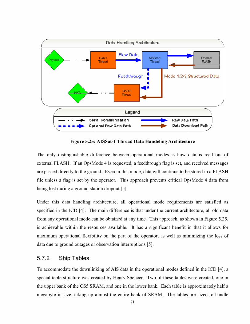
Figure 5.25: AISSat
The only distinguishable difference between
external FLASH. If an OpsMode 4
are passed directly to the ground. Even in this mode, dat
file unless a flag is set by the operator
being lost during a ground station dropout
Under this data handling architecture, all
specified in the ICD [4]. The main difference is that under the current architecture, all
from any operational mode can be obta
is achievable within the resources available. It has a significant benefit in that it allows for
maximum operational flexibility on the part of the operator, as well as minimizing the l
data due to ground outages or observation interruptions
5.7.2 Ship Tables
To accommodate the downlinking of AIS data in the operational modes defined
special table structure was created
the upper bank of the CS5 SRAM, and one in
megabyte in size, taking up 71
: AISSat-1 Thread Data Handeling Architecture
The only distinguishable difference between operational modes is how
OpsMode 4 is requested, a feedthrough flag is set, and received me
to the ground. Even in this mode, data will continue to be stored in a FLASH
file unless a flag is set by the operator. This approach prevents critical OpsMode 4
being lost during a ground station dropout [5].
Under this data handling architecture, all operational mode requirements are satisfied as
. The main difference is that under the current architecture, all
from any operational mode can be obtained at any time. This approach, as shown
achievable within the resources available. It has a significant benefit in that it allows for
maximum operational flexibility on the part of the operator, as well as minimizing the l
data due to ground outages or observation interruptions [5].
To accommodate the downlinking of AIS data in the operational modes defined
special table structure was created by Henry Spencer. Two of these tables
the upper bank of the CS5 SRAM, and one in the lower bank. Each table is approximately half a
up almost the entire bank of SRAM. The tables are sized to handle
Architecture
data is read out of
and received messages
a will continue to be stored in a FLASH
OpsMode 4 data from
operational mode requirements are satisfied as
. The main difference is that under the current architecture, all old data
. This approach, as shown in Figure 5.25,
achievable within the resources available. It has a significant benefit in that it allows for
maximum operational flexibility on the part of the operator, as well as minimizing the loss of
To accommodate the downlinking of AIS data in the operational modes defined in the ICD [4], a
. Two of these tables were created, one in
the lower bank. Each table is approximately half a
. The tables are sized to handle

72
more than 30,000 ships, exceeding the requirement of 20,000 with some margin. At any given
time, one of these tables is active, and the other is inactive. All new AIS data gets mapped into
the currently active table, while the inactive table is used to downlink old payload data, in the
desired operational mode format.
The table structure consists of a large hash table using the VDL CRC as its hashing function.
Each element in the hash table acts as the head of a list of ship structures. These structures keep
FLASH file pointers to the first and last message for each ship observed, as well as their latitude
[5].
5.7.3 AISSat-1 OBC Commands
In addition to the data handling functionality described in previous sections, the AISSat-1 Thread
also implements a set of commands. These commands execute various tasks, allowing the
operator on the ground to fully control the payload and its data flow.
5.7.3.1 AIS_OBC_TELEMETRY
The AIS_OBC_TELEMETRY command allows operators and application threads to request all
POBC telemetry through one command. Upon reception of the command, all telemetry will be
gathered and transmitted to the requesting party.
5.7.3.2 AIS_OBC_READ_INACTIVE_TABLE
The AIS_OBC_READ_INACTIVE_TABLE command allows the operator to initiate an
OpsMode 2 or 3 download. Based on the mode defined in the data field of the command, the
POBC will then use the inactive table to initiate a download of the requested type.
In addition to supporting full downloads, this command also supports the request of single
packets of a specific mode type. This allows dropped packets to be re-requested, without
restarting the entire download.
5.7.3.3 AIS_OBC_SET_INACTIVE_TABLE
The AIS_OBC_SET_INACTIVE_TABLE command allows operators to switch the currently
active table with the currently inactive table. Upon reception of this command, the currently
active table will be set to inactive, maintaining its contents so that OpsMode 2 or 3 data can be

73
obtained. The currently inactive table is then cleared, losing all of its data, and set as active.
During this process, the currently active payload data file is also closed, and a new file opened in
its place.
If an operator requests that a table be set inactive, when it is already the inactive table, the
command will receive a no-acknowledge. The POBC will continue to function in its current
state, collecting new payload data in the currently active table.
5.7.3.4 AIS_OBC_PARAMETER_QUERY
The AIS_OBC_PARAMETER_QUERY command allows operators to see various different
metrics and flags on the POBC. All modifiable flags used to control the flow of payload data are
contained here, which gives the operators the ability to confirm that a flag has been set. This
insures that no payload data will ever be lost due to a failure to set a flag. Notable flags that can
be observed through this command are; PPS_Generate, Feedthrough, Store_Data and
Table_Update.
5.7.3.5 AIS_OBC_PARAMETER_SET
The AIS_OBC_PARAMETER_SET command allows operators to modify flags, and various
other settable metrics. All modifiable flags used to control the flow of payload data are set with
this command. Notable flags that can be set through this command are; PPS_Generate,
Feedthrough, Store_Data and Table_Update.
If an operator attempts to set a value that is read only, the current value of that metric or flag
will be returned with a no-acknowledge.
5.7.3.6 AIS_OBC_SET_SENSOR_TIME
The AIS_OBC_SET_SENSOR_TIME command allows the operator to set the time on the AIS
sensor. The AIS sensor requires that the sensor set time command is received between PPS
pulses. This command is needed to meet this requirement, as the operator on the ground cannot
control when a direct sensor set time command will arrive at the sensor. To meet this
requirement, a sensor set time command is sent to the AIS sensor between PPS pulses.

74
As this command merely synchronizes the sensor set time command with the PPS, it is set up
such that the response from the AIS sensor will be sent to the ground, with no further
intervention by the AISSat-1 thread.
5.8 Time Tag Command Thread
5.8.1 Time Tag Architecture
Figure 5.26 is the high level architectural design of the on board time tag handling software for
the GNB nanosatellite missions. This architecture was developed by the author based originally
on the time tag architecture use in the NTS mission. Once the architecture was finalized, the
author was tasked with fully implementing it for use in the GNB missions.
Figure 5.26: High level Time Tag Architecture [6]
5.8.2 Time Tag Queuing
Time tag commands are executed sequentially from a queue that can support up to 512
commands. Each command is labeled with an execution time, specified to millisecond accuracy
in J2000 (Number of seconds after Jan 1 2000). The spacecraft only accepts commands in the
future, and deletes the command from the queue after execution. Multiple commands at exactly
the same time are allowed in the current architecture. While commands can be timed to the
millisecond, it is important to note that we are running a multi-threaded system, which will not
always allow a command to be processed to millisecond accuracy. In actual fact, commands will
likely be sent out in bursts of 200-300 ms groups [6].

75
If an executed command fails (e.g. a NAK response is given), then an error flag is set. The
NACK is then saved to the Log and time tag command execution halts until restarted by the
operator. If the Time Tagged Command (TTC) Stop NACK flag is set low, then operation
continues unaffected [6].
Time tag command handling is implemented as its own thread running in CANOE. An alarm
will be set in CANOE to trigger when the next time-tagged command in the sequence should be
handled [6].
5.8.3 Adding time Tagged Commands
Operators can load time tagged commands into the satellites queue through two separate
mechanisms. The first is a direct upload using the TTC_ADD command, which will put the
command directly on the queue. The other option is to upload a FLASH Script File, which is
essentially a sequence of commands with relative execution times. This script will remain idle in
FLASH until the TTC_LOAD command is sent. This command, using a base time located in its
data field, will add the contents of the script file to the queue [6].
5.8.4 Command Set
There are six commands pertaining to the Time Tag handling, shown in Table 5-4.
Command Value Description TTC_ADD 0x11 Enqueue a new time tagged command TTC_GET 0x12 Download single commands from the queue TTC_FLUSH 0x13 Delete one or all commands from the queue TTC_LOAD 0x14 Load a script from FLASH TTC_QSTATE 0x15 Returns the state of the queue TTC_SWAP_LOG 0x16 Close current log file and open a new one
Table 5-4: Time Tag Commands [6]
Furthermore, there are a number of on-board parameters which can be queried and set through
the Parameter Query and Parameter Set commands, respectively. These parameters are given in
Table 5-5.

76
Parameter Name ID Default Description R/W TTC Enable 0 0 Allow forwarding of commands R/W TTC Size 1 0 Number of commands in the table R TTC Error Code 2 0 Code of last error R/W TTC Stop NACK 3 0 Stop on NACK Flag R/W TTC NACK 4 0 Set if NACK Received R/W TTC Command Buffer Size 5 512 Settable Size for the command buffer R/W
Table 5-5: Time Tag Parameter Telemetry [6]
5.8.4.1 TTC_ADD
The TTC_ADD command allows operators or automated software to add time tagged commands
to the time tag queue. This is the simplest of the time tag commands, with only a time tag and
NSP packet contained within its data field.
In order to accommodate ACK/NACK logging, all commands contained in the NSP packet
within the TTC_ADD command must set their source address to the time tag thread address. If
ACK/NACK logging is not desired, this address can be set arbitrarily.
5.8.4.2 TTC_GET
The TTC_GET command gives the operator the ability to determine what commands are
currently in the time tag queue. This command has two forms, determined by the contents of the
data field.
When the data field of this command is empty, the time tag thread will return the execution times
of the first and last time tagged commands in the list.
When a specific time is given in the data field, the command set for that time is return, if any
exist in the queue.
This command does not give the user the ability to trace through the queue; its main use will be
in the confirmation process of time tag command uploading.

77
5.8.4.3 TTC_FLUSH
The TTC_FLUSH command gives the operator the ability to remove time tagged commands
from the queue. This command has two forms, determined by the contents of the data field.
When the data field contains an ERASE_ALL mask (currently 0xFFFFFFFFFF), the contents of
the entire queue are deleted. This allows the operator to flush the entire queue with a single
command.
When the data field contains a specific time, destination address and command, all commands
from that time slot with that specific address and command are removed from the queue. This
allows the operator to flush single commands from the queue, while preserving other commands
that exist in the same timeslot.
5.8.4.4 TTC_LOAD
The TTC_LOAD command allows the operator to load a set of commands from a script file
stored in external FLASH. The data field of the command contains the script file name, and a
base time. The base time is used to create absolute times from relative times found in the file.
The files stored in FLASH must be created by operators on the ground, and pre-loaded to the
satellite before the TTC_LOAD command is sent.
The TTC_LOAD command is intended to extend the capabilities of the time tag architecture, but
is not required for its functionality. Automated operations will likely make use of these script
files, to reduce the amount of time the ground station spends uploading commands.
5.8.4.5 TTC_QSTATE
The TTC_QSTATE command allows the operators to view the entire contents of the queue.
This command returns the number of commands in the queue, number of slots remaining and a
time ordered list of command/execution time pairs.
Only the command and destination address of each queued command will be downlinked to the
ground. The operator can request more information about specific commands using the
TTC_GET command.

78
5.8.4.6 TTC_SWAP_LOG
The TTC_SWAP_LOG command allows the operator to change the currently active time tag log
file. When this command is received, the current log file is closed, and a new one created in its
place.
Once this command has been executed, it is up to the operators on the ground to download and
delete the previous log from external FLASH.
5.8.5 Command Response Logging
Commands sent though time tag will not have the ground station available to receive any ACK
or NACKs created by those commands. Instead, a log file will exist in FLASH that will be used
to keep a detailed record of all ACKS/NACKS received from time tagged commands. In the
event that a NACK is received and the Stop on NACK flag is set, time tagged commands will
halt and the log file will be closed to ensure log data is not lost [6].

79
6 Discussion
A significant portion of the software discussed in this thesis went through several iterations
before reaching their final state. These iterations were caused by incorrect assumptions,
emerging requirements and inadequate development of the “True” software requirements.
The single most common reason for a piece of software needing re-development is the
assumption that the processor you are using is “fast enough” to execute your code. In real-time
embedded systems this assumptions usually turns out to be wrong. In the future, when
developing software for embedded systems it is highly recommended by the author that the
developer use the assumption that the processor you are using is not “fast enough” for your
application. Software developed using this approach tends to be simpler and performs far greater
in real-time space based applications. While taking this approach increases the amount of up
front engineering time required for software development, it also reduces the total time required
in the downstream software re-development phase.
Emerging software requirements are another major cause of software re-development. This
includes such things as the discovery of unforeseen hardware limitations, unexpected
modifications to the software’s functionality and last minute changes to the satellite mission
itself. All of these are issues the author dealt with during the development of the embedded
software for the GNB satellites. While emerging software requirements are inherently un-
predictable, measures can be taken to minimize the impact this has on the software development.
These measures include a flexible design architecture and adequate study into the potential uses
of that particular software development. Even if a particular piece of software is only required to
execute very specific tasks, it is beneficial to design that software to allow flexibility. Designing
for flexibility also increases the up front development time, but will once again reduce the time
required for downstream software re-development.
Software requirements are usually developed during the conceptual phase of a nanosatellite
mission, and thus tend to be more general. This can cause some issues in the software
development phase since what appears to be acceptable based on the requirements may not be
acceptable operationally. A requirement stating that a specific OBC must be able to downlink
over the S-Band transmitter is deceiving. This requirement says nothing about the data rate or

80
throughput of the S-Band downlink, which is very important operationally. Significant
engineering time can be saved if the developer does in in-depth study into each of the software
requirements to determine if there are deeper seeded requirements that need be imposed on their
design. This is especially important when operating under the microspace philosophy, where
heavy documentation does not always exist.
In the development of the time tag command thread, discussed in Section 5.8, all of the above
suggestions were used. The up front development time was significantly longer than in previous
developments, but the approach paid off. The time tag command thread was written only once,
with no revisions being required to date. This approach also allowed for a more detailed
interface control document to be created early in the development. This reduced the test phase of
the software development due to the fact that it allowed other engineers to complete the ground
support software in parallel with the development of the embedded software.
It is the hope of the author that some of the suggestions put forth will help reduced the overall
development time and complexity of embedded software design for future nanosatellite missions.

81
7 Conclusions
The Space Flight Laboratory is continuing to push the boundaries of what can be achieved with
nanosatellite technology. From AIS tracking in space to precision formation flying, the potential
is endless. With the successful launch of the CanX-2 mission, technological validation is paving
the way for the next generation of GNB derived CanX missions. The current GNB satellites in
development include AISSat-1, CanX-3 (BRITE) and CanX-4&5. AISSat-1 is a space based
AIS tracking satellite, destined to monitor ship traffic in Norwegian waters. CanX-3 (BRITE) is
a constellation of stellar photometry missions, destined to study the varying intensity of stars.
CanX-4&5 is a formation flying mission, intended to show that sub meter formation flying can
be accomplished on a nanosatellite platform.
This thesis presented a detailed summary of the author’s contribution to the GNB line of CanX
nanosatellite missions. Major contributions included the validation of the on-board computer
design for the AISSat-1 mission and development and testing of a substantial portion of the GNB
flight software. Software development for the validation of the on-board computer demonstrated
that the design met the AISSat-1 mission requirements with ample margin, giving our Norwegian
clients great confidence in the potential success of the mission. The software designed for the
GNB platform will enable any and all GNB missions to reduce non-recurring engineering costs
greatly, due to its generic nature. In addition to reducing costs in the future, the authors work
will form the foundation of the flight software for the AISSat-1, CanX-3 (BRITE) and CanX-
4&5 missions. While final designs were presented, the motivation and reasoning for those
designs were also given where possible. It is the hope of the author that the information
provided within will assist in the development of future nanosatellite missions.

82
References or Bibliography
[1] Dwyer, M. “AISSat-1 Payload Computer Software Requirements.” Unpublished internal document. Reference number SFL-AIS-OBC-R003, Dec 18/2007.
[2] Kekez, D.“Nanosatellite Protocol (NSP) Version 3.” Unpublished internal document. Reference number SFL-GNB-OBC-D001, Feb 13/2009.
[3] Beattie, A. “AISSat-1 Mission Definition and System Requirements Document.”
Unpublished internal document. Reference number SFL-AIS-SYS-R002, Jan 13/2008. [4] Beattie, A. “AISSat-1 Payload Interface Control Document.” Unpublished internal
document. Reference number SFL-AIS-SYS-ICD002, Apr 21/2008. [5] Dwyer, M. “AISSat-1 Payload Computer Software Design.” Unpublished internal
document. Reference number SFL-AIS-OBC-003, Jan 7/2008. [6] Dwyer, M. “GNB Time Tag Interface Control Document.” Unpublished internal
document. Reference number [Undefined], May 22/2009. [7] Grant, C. “GNB Ground Software Requirements TimeTag.” UTIAS Unpublished internal
document. Reference number SFL-GNB-SYS-R016, 4 May 2009.
[8] Radiation Effects & Analysis. [Online]. Available: http://radhome.gsfc.nasa.gov/radhome/see.htm
[9] Low-pass filter. [Online]. Available: http://en.wikipedia.org/wiki/Low-pass_filter
[10] Orr, N. “Genaric Nanosatellite Bus Power Controller Overview.” UTIAS Unpublished
internal document. Reference number SFL-GNB-PWR-001, 15 Dec 2008.
[11] Tuli, T. “BRITE and CanX-4/CanX-5 Software Subsystem Requirements.” UTIAS Unpublished internal document. Reference number SFL-GNB-SYS-R007, 27 Arp 2007.
[12] Tuli, T. “AISSat-1 On-Board Computer Design Document.” UTIAS Unpublished internal
document. Reference number SFL-AIS-OBC-D001, 19 Jan 2008. [13] Carufel, G. “Assembly, Integration and Thermal Testing of the Genaric Nanosatellite
Bus.” UTIAS Master’s Thesis, 2009. [14] Orr, N. “Development and Testing of the Power and Software Subsystems for the
Canadian Advanced Nanospace Experiment.” UTIAS Masters Thesis, 2007 [15] Beattie, A. “Structural Design of AISSat-1.” UTIAS Unpublished internal document.
Reference number SFL-AIS-STR-D001, 21 Apr 2008.

83
[16] Eagleson, S. “AISSat-1 Attitude Determination and Control Design Document.” UTIAS
Unpublished internal document. Reference number SFL-AIS-ACS-D001, 21 Apr 2008. [17] Beattie, A. “AISSat-1 Communication System Design Document.” UTIAS Unpublished
internal document. Reference number SFL-AIS-COM-D001, 21 Apr 2008. [18] Mok, C. “Design and Implementation of the Flight Application Software and
NanoSatellite Protocol for the CanX-2 Nanosatellite.” UTIAS Masters Thesis, 2005