Electronic structure and optical properties of ZnX (X=O, S, Se, Te): A
14
Electronic structure and optical properties of ZnX (X =O, S, Se, Te): A density functional study S. Zh. Karazhanov, 1,2 P. Ravindran, 1 A. Kjekshus, 1 H. Fjellvåg, 1 and B. G. Svensson 3 1 Centre for Material Science and Nanotechnology, Department of Chemistry, University of Oslo, P.O. Box 1033 Blindern, N-0315 Oslo, Norway 2 Physical-Technical Institute, 2B Mavlyanov Street, Tashkent 700084, Uzbekistan 3 Department of Physics, University of Oslo, P.O. Box 1048 Blindern, N-0316 Oslo, Norway Received 5 July 2006; revised manuscript received 15 November 2006; published 6 April 2007 Electronic band structure and optical properties of zinc monochalcogenides with zinc-blende- and wurtzite- type structures were studied using the ab initio density functional method within the local-density approxima- tion LDA, generalized-gradient approximation, and LDA+ U approaches. Calculations of the optical spectra have been performed for the energy range 0 – 20 eV, with and without including spin-orbit coupling. Reflec- tivity, absorption and extinction coefficients, and refractive index have been computed from the imaginary part of the dielectric function using the Kramers-Kronig transformations. A rigid shift of the calculated optical spectra is found to provide a good first approximation to reproduce experimental observations for almost all the zinc monochalcogenide phases considered. By inspection of the calculated and experimentally determined band-gap values for the zinc monochalcogenide series, the band gap of ZnO with zinc-blende structure has been estimated. DOI: 10.1103/PhysRevB.75.155104 PACS numbers: 71.15.m, 71.22.i I. INTRODUCTION The zinc monochalcogenides ZnX; X =O, S, Se, and Te are the prototype II-VI semiconductors. These compounds are reported to crystallize in the zinc-blende-z and wurtzite w-type structures. The ZnX-z phases are optically isotropic, while the ZnX-w phases are anisotropic with c as the polar axis. ZnX phases are a primary candidate for optical device technology such as visual displays, high-density optical memories, transparent conductors, solid-state laser devices, photodetectors, solar cells, etc. So, knowledge about optical properties of these materials is especially important in the design and analysis of ZnX-based optoelectronic devices. Optical parameters for some of the ZnX phases have widely been studied experimentally in the past. Detailed in- formation on this subject is available for ZnO-w, 1–9 ZnS-w, 9 ZnS-z, 9–11 ZnSe-z, 9,10 and ZnTe-z, 9,10,12,13 and see the sys- tematized survey in Ref. 14. However, there are no experi- mental data on optical properties of ZnSe-w, ZnTe-w, and ZnO-z. Furthermore, there is a lack of consistency between some of the experimental values for the optical spectra. This is demonstrated in Fig. 1, which displays reflectivity spectra for ZnO-w measured at T =300 K by three different groups. Dielectric-response functions were calculated using the Kramers-Kronig relation. As is seen in Fig. 1, intensity of the imaginary part of the dielectric function 2 and reflectivity R corresponding to the fundamental absorption edge of ZnO-w are higher 8 than those at the energy range 10–15 eV, while in Ref. 14 it is vice versa. The optical spectra in Fig. 1 measured using the linearly polarized incident light for elec- tric field E parallel and perpendicular to the c axes are somehow close to those of Ref. 7 using nonpolarized incident light. Using the experimental reflectivity data, a full set of op- tical spectra for ZnO has been calculated 15 for the wide en- ergy range 0 – 26 eV. Density functional theory 16 DFT in the local-density approximation 17 LDA has also been used to calculate optical spectra for ZnO-w Ref. 18 and ZnS-w Ref. 18 by linear combination of atomic orbitals and for ZnS-z 19 and ZnSe-z 19 by self-consistent linear combination of Gaussian orbitals. The optical spectra of ZnO including excitons has been investigated 20 by solving the Bethe- Salpeter equation. Band-structure studies have been per- formed by linearized-augmented plane-wave method plus lo- cal orbitals LAPW+LO within the generalized gradient and LDA with the multiorbital mean-field Hubbard potential LDA+ U approximations. The latter approximation is found to correct not only the energy location of the Zn 3d electrons and associated band parameters see also Refs. 21 and 22 but also to improve the optical response. Despite the shortcoming of DFT in relation to underestimation of band gaps, the locations of the major peaks in the calculated en- ergy dependence of the optical spectra are found to be in good agreement with experimental data. It should be noted that the error in calculation of the band gap by DFT within LDA and generalized-gradient approxi- mation GGA is more severe in semiconductors with strong Coulomb correlation effects than in other solids. 21–25 This is due to the mean-field character of the Kohn-Sham equations and the poor description of the strong Coulomb correlation and exchange interaction between electrons in narrow d bands viz., the potential U. Not only the band gap E g but also the crystal-field CF and spin-orbit SO splitting ener- gies CF and SO , the order of states at the top of the valence band VB, the location of the Zn 3d band and its width, and the band dispersion are found 21,22,26,27 to be incor- rect for ZnO-w by the ab initio full potential FP and atomic-sphere-approximation ASA linear muffin-tin orbital LMTO methods within the pure LDA Refs. 26 and 27 and by the projector-augmented wave PAW method within LDA and GGA. 21,22 These findings were ascribed 21,22 to strong Coulomb correlation effects. DFT calculations within LDA plus self-interaction correction LDA+SIC and LDA + U are found 21,22,26 to rectify the errors related to CF and PHYSICAL REVIEW B 75, 155104 2007 1098-0121/2007/7515/15510414 ©2007 The American Physical Society 155104-1
Transcript of Electronic structure and optical properties of ZnX (X=O, S, Se, Te): A

Electronic structure and optical properties of ZnX (X=O, S, Se, Te): A density functional study
S. Zh. Karazhanov,1,2 P. Ravindran,1 A. Kjekshus,1 H. Fjellvåg,1 and B. G. Svensson3
1Centre for Material Science and Nanotechnology, Department of Chemistry, University of Oslo, P.O. Box 1033 Blindern,N-0315 Oslo, Norway
2Physical-Technical Institute, 2B Mavlyanov Street, Tashkent 700084, Uzbekistan3Department of Physics, University of Oslo, P.O. Box 1048 Blindern, N-0316 Oslo, Norway
�Received 5 July 2006; revised manuscript received 15 November 2006; published 6 April 2007�
Electronic band structure and optical properties of zinc monochalcogenides with zinc-blende- and wurtzite-type structures were studied using the ab initio density functional method within the local-density approxima-tion �LDA�, generalized-gradient approximation, and LDA+U approaches. Calculations of the optical spectrahave been performed for the energy range 0–20 eV, with and without including spin-orbit coupling. Reflec-tivity, absorption and extinction coefficients, and refractive index have been computed from the imaginary partof the dielectric function using the Kramers-Kronig transformations. A rigid shift of the calculated opticalspectra is found to provide a good first approximation to reproduce experimental observations for almost all thezinc monochalcogenide phases considered. By inspection of the calculated and experimentally determinedband-gap values for the zinc monochalcogenide series, the band gap of ZnO with zinc-blende structure hasbeen estimated.
DOI: 10.1103/PhysRevB.75.155104 PACS number�s�: 71.15.�m, 71.22.�i
I. INTRODUCTION
The zinc monochalcogenides �ZnX; X=O, S, Se, and Te�are the prototype II-VI semiconductors. These compoundsare reported to crystallize in the zinc-blende-�z� and wurtzite�w�-type structures. The ZnX-z phases are optically isotropic,while the ZnX-w phases are anisotropic with c as the polaraxis. ZnX phases are a primary candidate for optical devicetechnology such as visual displays, high-density opticalmemories, transparent conductors, solid-state laser devices,photodetectors, solar cells, etc. So, knowledge about opticalproperties of these materials is especially important in thedesign and analysis of ZnX-based optoelectronic devices.
Optical parameters for some of the ZnX phases havewidely been studied experimentally in the past. Detailed in-formation on this subject is available for ZnO-w,1–9 ZnS-w,9
ZnS-z,9–11 ZnSe-z,9,10 and ZnTe-z,9,10,12,13 and see the sys-tematized survey in Ref. 14. However, there are no experi-mental data on optical properties of ZnSe-w, ZnTe-w, andZnO-z. Furthermore, there is a lack of consistency betweensome of the experimental values for the optical spectra. Thisis demonstrated in Fig. 1, which displays reflectivity spectrafor ZnO-w measured at T=300 K by three different groups.Dielectric-response functions were calculated using theKramers-Kronig relation. As is seen in Fig. 1, intensity of theimaginary part of the dielectric function ��2� and reflectivity�R� corresponding to the fundamental absorption edge ofZnO-w are higher8 than those at the energy range 10–15 eV,while in Ref. 14 it is vice versa. The optical spectra in Fig. 1measured using the linearly polarized incident light for elec-tric field �E� parallel ��� and perpendicular ��� to the c axesare somehow close to those of Ref. 7 using nonpolarizedincident light.
Using the experimental reflectivity data, a full set of op-tical spectra for ZnO has been calculated15 for the wide en-ergy range 0–26 eV. Density functional theory16 �DFT� inthe local-density approximation17 �LDA� has also been used
to calculate optical spectra for ZnO-w �Ref. 18� and ZnS-w�Ref. 18� by linear combination of atomic orbitals and forZnS-z19 and ZnSe-z19 by self-consistent linear combinationof Gaussian orbitals. The optical spectra of ZnO �includingexcitons� has been investigated20 by solving the Bethe-Salpeter equation. Band-structure studies have been per-formed by linearized-augmented plane-wave method plus lo-cal orbitals �LAPW+LO� within the generalized gradientand LDA with the multiorbital mean-field Hubbard potential�LDA+U� approximations. The latter approximation isfound to correct not only the energy location of the Zn 3delectrons and associated band parameters �see also Refs. 21and 22� but also to improve the optical response. Despite theshortcoming of DFT in relation to underestimation of bandgaps, the locations of the major peaks in the calculated en-ergy dependence of the optical spectra are found to be ingood agreement with experimental data.
It should be noted that the error in calculation of the bandgap by DFT within LDA and generalized-gradient approxi-mation �GGA� is more severe in semiconductors with strongCoulomb correlation effects than in other solids.21–25 This isdue to the mean-field character of the Kohn-Sham equationsand the poor description of the strong Coulomb correlationand exchange interaction between electrons in narrow dbands �viz., the potential U�. Not only the band gap �Eg� butalso the crystal-field �CF� and spin-orbit �SO� splitting ener-gies ��CF and �SO�, the order of states at the top of thevalence band �VB�, the location of the Zn 3d band and itswidth, and the band dispersion are found21,22,26,27 to be incor-rect for ZnO-w by the ab initio full potential �FP� andatomic-sphere-approximation �ASA� linear muffin-tin orbital�LMTO� methods within the pure LDA �Refs. 26 and 27� andby the projector-augmented wave �PAW� method withinLDA and GGA.21,22 These findings were ascribed21,22 tostrong Coulomb correlation effects. DFT calculations withinLDA plus self-interaction correction �LDA+SIC� and LDA+U are found21,22,26 to rectify the errors related to �CF and
PHYSICAL REVIEW B 75, 155104 �2007�
1098-0121/2007/75�15�/155104�14� ©2007 The American Physical Society155104-1

�SO, order of states at the top VB, and width and location ofthe Zn 3d band, as well as effective masses. In other semi-conductors, in which the Coulomb correlation is not suffi-ciently strong, the �CF and �SO values derived from DFTcalculations within LDA are found to be quite accurate. Thiswas demonstrated for diamondlike group IV, z-type groupIII-V, II-VI, and I-VII semiconductors,28 w-type AlN, GaN,and InN,29 using the LAPW and VASP-PAW, the w-type CdSand CdSe,27 z-type ZnSe, CdTe, and HgTe,30 using the abinitio LMTO-ASA, and z- and w-type ZnSe and ZnTe �Refs.21 and 22� as well as z-type CdTe,31 using the VASP-PAWand FP LMTO methods. Although the SO splitting at thetop of VB is known to play an important role in electronicstructure and chemical bonding ofsemiconductors,21,22,26,28–30,32,33 there is no systematic studyof the role of the SO coupling in optical properties of thesematerials.
Several attempts have been undertaken to resolve the DFTeigenvalue problem. One such approach is the utilization ofthe GW approximation �“G” stands for one-particle Green’sfunction as derived from many-body perturbation theory and“W” for Coulomb screened interactions�. Although GW re-moves most of the problems of LDA with regard to excited-state properties, it fails to describe the semiconductors withstrong Coulomb correlation effects. For example, two studiesof the band gap of ZnO calculated using the GW correctionunderestimated Eg by 1.2 eV �Ref. 34� and overestimated itby 0.84 eV.35 Calculations for Zn, Cd, and Hg monochalco-genides by the GW approach showed36 that the band-gapunderestimation is in the range 0.3–0.6 eV. Combination ofexact-exchange �EXX� DFT calculations and the optimized-effective GW potential approach is found37 to improve theagreement with the experimental band gaps and Zn 3d en-ergy levels. Band gaps calculated within the EXX treatmentare found to be in good agreement with experiment for the
s-p semiconductors.38,39 Excellent agreement with experi-mental data was obtained39 also for locations of energy levelsof the d bands of a number of semiconductors and insulatorssuch as Ge, GaAs, CdS, Si, ZnS, C, BN, Ne, Ar, Kr, and Xe.
Another means to correct the DFT eigenvalue error is touse the screened-exchange LDA.40 Compared to LDA andGW, this approximation is found to be computationally muchless demanding, permitting self-consistent determination ofthe ground-state properties and giving more correct bandgaps and optical properties. Other considered approaches forab initio computations of optical properties involve electron-hole interaction,41 partial inclusion of dynamical vertex cor-rections that neglect excitons,42 and empirical energy-dependent self-energy correction according to the Kohn-Sham local-density theory of excitation.19 However, thesimplest method is to apply the scissor operator,43 whichdisplaces the LDA eigenvalues for the unoccupied states by arigid energy shift. Using the latter method, excellent agree-ment with experiments has been demonstrated for leadmonochalcogenides44 and ferroelectric NaNO2.45 However,the question as to whether the rigid energy shift is generallyapplicable to semiconductors with strong Coulomb correla-tion effects is open.
In this work, electronic structure and optical properties ofthe ZnX-w and -z phases have been studied in the energyrange from 0 to 20 eV based on first-principles band-structure calculations derived from DFT within the LDA,GGA, and LDA+U.
II. COMPUTATIONAL DETAILS
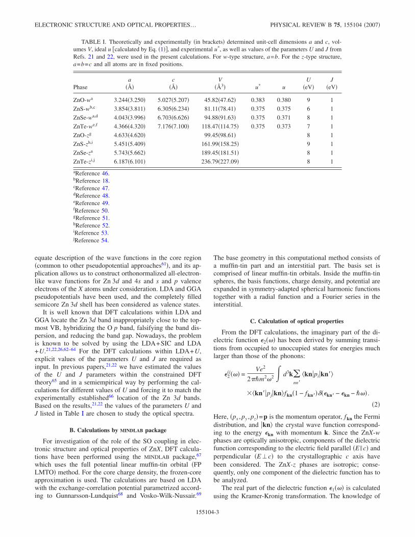
Experimentally determined lattice parameters have beenused in the present ab initio calculations �Table I�. The idealpositional parameter u for ZnX-w is calculated on the as-sumption of equal nearest-neighbor bond lengths:27
u =1
3�a
c�2
+1
4. �1�
The values of u for the ideal case agree well with the experi-mental values u* �see Table I�. Self-consistent calculationswere performed using a 10�10�10 mesh according to theMonkhorst-Pack scheme for the ZnX-z phases and the�-centered grid for the ZnX-w phases.
A. Calculations by VASP package
Optical spectra have been studied based on the band-structure data obtained from the VASP-PAW package,55 whichsolves the Kohn-Sham eigenvalues in the framework of theDFT �Ref. 16� within LDA,17 GGA,56 and the simplified ro-tationally invariant LDA+U.23,24 The exchange and correla-tion energies per electron have been described by thePerdew-Zunger parametrization57 of the quantum MonteCarlo results of Ceperley and Alder.58 The interaction be-tween electrons and atomic cores is described by means ofnon-norm-conserving pseudopotentials implemented in theVASP package.55 The pseudopotentials are generated in accor-dance with the PAW �Refs. 59 and 60� method. The use ofthe PAW pseudopotentials addresses the problem of inad-
FIG. 1. Reflectivity spectra R��� for ZnO-w determined experi-mentally at 300 K in Refs. 9 and 14 �solid circles�, Ref. 8 �opencircles�, and Ref. 7 �solid lines�, along with the imaginary part ofthe dielectric-response function ��2���� calculated using theKramers-Kronig relation. The results of Ref. 7 �open circles� areused for both E �c and E�c, because no polarized incident lightwas used in the experiments.
KARAZHANOV et al. PHYSICAL REVIEW B 75, 155104 �2007�
155104-2
equate description of the wave functions in the core region�common to other pseudopotential approaches61�, and its ap-plication allows us to construct orthonormalized all-electron-like wave functions for Zn 3d and 4s and s and p valenceelectrons of the X atoms under consideration. LDA and GGApseudopotentials have been used, and the completely filledsemicore Zn 3d shell has been considered as valence states.
It is well known that DFT calculations within LDA andGGA locate the Zn 3d band inappropriately close to the top-most VB, hybridizing the O p band, falsifying the band dis-persion, and reducing the band gap. Nowadays, the problemis known to be solved by using the LDA+SIC and LDA+U.21,22,26,62–64 For the DFT calculations within LDA+U,explicit values of the parameters U and J are required asinput. In previous papers,21,22 we have estimated the valuesof the U and J parameters within the constrained DFTtheory65 and in a semiempirical way by performing the cal-culations for different values of U and forcing it to match theexperimentally established66 location of the Zn 3d bands.Based on the results,21,22 the values of the parameters U andJ listed in Table I are chosen to study the optical spectra.
B. Calculations by MINDLAB package
For investigation of the role of the SO coupling in elec-tronic structure and optical properties of ZnX, DFT calcula-tions have been performed using the MINDLAB package,67
which uses the full potential linear muffin-tin orbital �FPLMTO� method. For the core charge density, the frozen-coreapproximation is used. The calculations are based on LDAwith the exchange-correlation potential parametrized accord-ing to Gunnarsson-Lundquist68 and Vosko-Wilk-Nussair.69
The base geometry in this computational method consists ofa muffin-tin part and an interstitial part. The basis set iscomprised of linear muffin-tin orbitals. Inside the muffin-tinspheres, the basis functions, charge density, and potential areexpanded in symmetry-adapted spherical harmonic functionstogether with a radial function and a Fourier series in theinterstitial.
C. Calculation of optical properties
From the DFT calculations, the imaginary part of the di-electric function �2��� has been derived by summing transi-tions from occupied to unoccupied states for energies muchlarger than those of the phonons:
�2ij��� =
Ve2
2�m2�2 � d3knn�
kn�pi�kn��
�kn��pj�kn�fkn�1 − fkn����kn� − �kn − �� .
�2�
Here, �px , py , pz�=p is the momentum operator, fkn the Fermidistribution, and �kn� the crystal wave function correspond-ing to the energy �kn with momentum k. Since the ZnX-wphases are optically anisotropic, components of the dielectricfunction corresponding to the electric field parallel �E �c� andperpendicular �E�c� to the crystallographic c axis havebeen considered. The ZnX-z phases are isotropic; conse-quently, only one component of the dielectric function has tobe analyzed.
The real part of the dielectric function �1��� is calculatedusing the Kramer-Kronig transformation. The knowledge of
TABLE I. Theoretically and experimentally �in brackets� determined unit-cell dimensions a and c, vol-umes V, ideal u �calculated by Eq. �1��, and experimental u*, as well as values of the parameters U and J fromRefs. 21 and 22, were used in the present calculations. For w-type structure, a=b. For the z-type structure,a=b=c and all atoms are in fixed positions.
Phasea
��c
��V
�Å3� u* uU
�eV�J
�eV�
ZnO-wa 3.244�3.250� 5.027�5.207� 45.82�47.62� 0.383 0.380 9 1
ZnS-wb,c 3.854�3.811� 6.305�6.234� 81.11�78.41� 0.375 0.375 6 1
ZnSe-wa,d 4.043�3.996� 6.703�6.626� 94.88�91.63� 0.375 0.371 8 1
ZnTe-we,f 4.366�4.320� 7.176�7.100� 118.47�114.75� 0.375 0.373 7 1
ZnO-zg 4.633�4.620� 99.45�98.61� 8 1
ZnS-zh,i 5.451�5.409� 161.99�158.25� 9 1
ZnSe-za 5.743�5.662� 189.45�181.51� 8 1
ZnTe-zi,j 6.187�6.101� 236.79�227.09� 8 1
aReference 46.bReference 18.cReference 47.dReference 48.eReference 49.fReference 50.gReference 51.hReference 52.iReference 53.jReference 54.
ELECTRONIC STRUCTURE AND OPTICAL PROPERTIES… PHYSICAL REVIEW B 75, 155104 �2007�
155104-3

both the real and imaginary parts of the dielectric tensorallows one to calculate other important optical spectra. Inthis paper, we present and analyze the reflectivity R���, theabsorption coefficient ����, the refractive index n���, andthe extinction coefficient k���:
R��� = ����� − 1����� + 1
2
, �3�
���� = ��2��12��� + �2
2��� − 2�1��� , �4�
n��� =���12��� + �2
2��� + �1���
2, �5�
k��� =���12��� + �2
2��� − �1���
2. �6�
Here, ����=�1���+ i�2��� is the complex dielectric function.The calculated optical spectra yield unbroadened functionsand, consequently, have more structure than the experimentalones.44,45,70,71 To facilitate a comparison with the experimen-tal findings, the calculated imaginary part of the dielectricfunction has been broadened. The exact form of the broad-ening function is unknown. However, analysis of the avail-able experimentally measured optical spectra of ZnX showsthat the broadening usually increases with increasing excita-tion energy. Also, the instrumental resolution smears outmany fine features. These features have been modeled usingthe lifetime broadening technique by convoluting the imagi-nary part of the dielectric function with a Lorentzian with afull width at half maximum of 0.002���2 eV, increasingquadratically with the photon energy. The experimental reso-lution was simulated by broadening the final spectra with aGaussian, where the full width at half maximum is equal to0.08 eV.
III. RESULTS AND DISCUSSION
A. Band structure
The optical spectra are related to band dispersion andprobabilities of interband optical transitions. So, it is of in-terest to analyze the electronic structure in detail. Band dis-persions for ZnX-w and ZnX-z calculated by DFT withinLDA and LDA+U are presented in Fig. 2. The general fea-tures of the band dispersions are in agreement with previousstudies �see, e.g., Refs. 26, 62, and 72�. It is seen from Fig. 2that the conduction-band �CB� minima for ZnX-w and ZnX-zare much more dispersive than the VB maximum, whichshows that the holes are much heavier than the CB electronsin agreement with experimental data73,74 for the effectivemasses and calculated with FP LMTO and �Ref. 26� linearcombination of atomic orbitals,18 as well as with ourfindings.21,21 Consequently, mobility of electrons is higherthan that of holes. Furthermore, these features indicate that pelectrons of X �that form the topmost VB states� are tightlybound to their atoms and make the VB holes less mobile.
Hence, the contribution of the holes to the conductivity isexpected to be smaller than that of CB electrons even thoughthe concentration of the latter is smaller than that of theformer. These features emphasize the predominant ionic na-ture of the chemical bonding. Another interesting feature ofthe band structures is that the VB maximum becomes moredispersive with increasing atomic number of X from O to Te.
As noted in our previous contributions,21,22 the band gapsof ZnX calculated by DFT within LDA, GGA, and LDA+U are underestimated and the question as to whether it ispossible to shift the CB states rigidly was kept open. Asfound from the optical spectra discussed on the followingsections, rigid shifts of the CB states up to the experimen-tally determined locations can provide a good first approxi-mation for the stipulation of the band gap. So, for the banddispersions in Fig. 2, we have made use of this simple wayfor correcting the band gaps calculated by DFT. The onlyproblem in this respect was the lack of an experimentalband-gap value for ZnO-z. To solve this problem, the experi-mental and calculated �by DFT within LDA� band gaps �Eg�of the ZnX series were plotted as a function of the atomicnumber of X. As seen from Fig. 3, Eg for the ZnX-w phasesare very close to the corresponding values for the ZnX-zphases and the shape of the experimental and calculatedfunctional dependencies is in conformity. On this basis, the
FIG. 2. Band dispersion for ZnO-w, ZnS-w, ZnSe-w, ZnTe-w,ZnO-z, ZnS-z, ZnSe-z, and ZnTe-z calculated according to LDA�solid lines� and LDA+U �dotted lines�. The Fermi level is set tozero energy.
KARAZHANOV et al. PHYSICAL REVIEW B 75, 155104 �2007�
155104-4

band gap of ZnO-z is estimated by extrapolating the findingsfor ZnX-z from ZnS-z to ZnO-z. This procedure gave Eg�3.3 eV for ZnO-z.
It is well known that not only band gaps are underesti-mated within LDA and GGA, but also band dispersionscome out incorrectly, whereas location of energy levels ofthe Zn 3d electrons are overestimated �see, e.g., Refs. 20–22and 63�. As also seen from Fig. 2, calculations within theLDA+U approach somewhat correct the location of the en-ergy levels of the Zn 3d electrons. The elucidation of theeigenvalue problem and the order of states at the topmost VBfrom LDA, GGA, and LDA+U calculations are discussed inRefs. 20–22 and 26 and will not be repeated here.
Examination of Fig. 2 shows that the VB comprises threeregions of bands: first a lower region consists of s bands ofZn and X, a higher-lying region of well localized Zn 3dbands, and on top of this a broader band dispersion originat-ing from X-p states hybridized with Zn 3d states. The lattersubband is more pronounced in ZnO than in the other ZnXphases considered. The hybridization is most severe accord-ing to the LDA and GGA calculations, whereas the LDA+U calculations somehow suppress this and improve theband-gap underestimation. A more detailed discussion ofthese aspects is found in Refs. 21 and 22.
The SO splitting at the topmost VB is known to play animportant role for the electronic structure and chemicalbonding of solids.28,29,32 In semiconductors with z-type struc-ture, the SO splitting energy is determined as the differencebetween energies of the topmost VB states with symmetry�8v and �7v.28,29,32 In the w-type compounds, the topmost VBis split not only by SO interaction but also by CF, giving riseto three states at the Brillouin-zone center. To calculate the
SO splitting energy for w-type phases, the quasicubic modelof Hopfield75 is commonly used.
It is well known that the SO splitting energy derived fromab initio calculations agrees well with experimental dataonly for some of the semiconductors. This is demonstrated,for example, for all diamondlike group IV and z-type groupIII-V, II-VI, and I-VII semiconductors,28 w-type AlN, GaN,and InN,29 ZnX-w and -z �X=S, Se, and Te�,21,22 and CdTe.31
However, the errors in estimated SO and CF splitting ener-gies by LDA calculations are significant for semiconductorswith strong Coulomb correlation effects, as demonstrated,e.g., for ZnO.21,22,26 For such systems, DFT calculationswithin LDA+U �Refs. 21, 22, and 26� are shown to providequite accurate values for �CF and �SO. Overestimation of thep-d hybridization in various variants of the DFT can alsolead to the wrong spin-orbit coupling of the valencebands.76,77
Systematic study of the SO coupling parameters was per-formed for zinc-blende II-VI semiconductors �Ref. 30� usingthe TB and LMTO methods, as well as for all diamondlikeand zinc-blende semiconductors �Ref. 28� using the FLAPWmethod with and without the p1/2 local orbitals and thefrozen-core PAW method implemented into VASP. The cor-rections coming from the inclusion of the local p1/2 orbitalsare found to be negligible for the compounds with light at-oms. Analysis of these results shows that the SO splittingenergy coming from calculations using the VASP-PAW showsgood agreement with the experimental data. This result wasalso obtained21 recently for ZnX of wurtzite and zinc-blendestructures. As demonstrated in Refs. 21 and 22 the SO split-ting energy ��SO� increases when one moves from ZnO-z toZnTe-z, in agreement with earlier findings of Ref. 28.
To study the role of the SO coupling in band dispersion,the present ab initio calculations have been performed byVASP and MINDLAB packages and spin-orbit splitting energyis found. The results are presented in Table II. Analysis ofTable II shows that ��SO� calculated by MINDLAB is quiteaccurate.
As expected, band dispersions calculated with and with-out the SO coupling differ little when the SO splitting energy
FIG. 3. Band gaps for Zn X-w �circles� and Zn X-z �triangles�phases determined experimentally �filled symbols, from Refs. 21and 22� and calculated �open symbols� by DFT within LDA as afunction of the atomic number of the X component of ZnX.
TABLE II. Calculated SO splitting energy �in meV� using theMINDLAB package along with the previous theoretical and experi-mental findings.
ZnO-z ZnS-z ZnSe-z ZnTe-z
–31 66 432 914
–31 66 432 914
−34a 66a 393a 889a
−34b 66b 398b 916b
−37c 64c 392c 898c
−33d 64d 393d 897d
65e 420f 910f
aLAPW, Ref. 28.bLAPW+ p1/2, Ref. 28.cVASP-PAW, Ref. 28.dVASP-PAW, Ref. 21.eExperiment, Ref. 78.fExperiment, Ref. 79.
ELECTRONIC STRUCTURE AND OPTICAL PROPERTIES… PHYSICAL REVIEW B 75, 155104 �2007�
155104-5

is small. However, the difference increases when one movesfrom ZnO to ZnTe. This feature is demonstrated in Table IIand Fig. 4 for band dispersions of ZnO-z, ZnO-w, ZnTe-z,and ZnTe-w calculated by VASP with and without includingthe SO coupling. As is well known �see, e.g., Refs. 21, 26,and 27�, without the SO coupling, the top of the VB ofZnX-w is split into a doublet and a singlet state. In the bandstructure, the Fermi level is located at the topmost one �Fig.4�, which is the zero energy. Upon inclusion of the SO cou-pling into calculations, the doublet and singlet states are splitinto three twofold degenerate states called A, B, and C stateswith energies Eg�A�, Eg�B�, and Eg�C�, respectively,80 ar-ranged in order of decreasing energy, i.e., Eg�A��Eg�B��Eg�C�. The center of gravity of the A, B, and C states,located at �Eg�A�−Eg�C�� /3 below the topmost A state, re-mains to be nearly the same as the topmost VB, correspond-ing to the case without the SO coupling.26,27 Consequently, tocompare band structures calculated with and without the SOcoupling, one should plot the band structure with the Fermienergy at the center of gravity of the A, B, and C states forthe former and at the topmost VB for the latter. Hence, whenthe SO coupling is applied, the A and B states as well as thebottommost CB move upwards to �Eg�A�−Eg�C�� /3 in en-ergy, whereas the C state moves downwards to �Eg�A�−Eg�C��2/3 compared to the center of gravity. Then, posi-tions of the lowest VB region calculated with and without theSO coupling remain nearly identical.
B. General features of optical spectra of ZnX
Since optical properties of solids are based on the bandstructure, the nature of the basic peaks in the optical spectra
can be interpreted in terms of the interband transitions re-sponsible for the peaks. Such an interpretation is availablefor semiconductors with z- and w-type structures.11,14,81 Inorder to simplify the presentation of the findings of thiswork, the labels E0, E1, and E2 of Ref. 11 �from the reflec-tivity spectra� were retained in Table III and Fig. 4. Thesubscript 0 is ascribed to transitions occurring at �, the sub-script 1 to transitions at points in the �111� direction, and thesubscript 2 to transitions at points in the �100� direction �re-ferring to the k space for the z-type structure�. Assignment ofthe E0, E1, and E2 peaks to optical transitions at high-symmetry points is presented in Table III and Fig. 4.
The optical spectra �1���, �2���, ����, R���, n���, andk��� calculated by DFT within LDA, GGA, and LDA+U aredisplayed in Figs. 5–8 and compared with available experi-mental findings.14 The spectral profiles are indeed very simi-lar to each other. Therefore, we shall only give a brief ac-count mainly focusing on the location of the interbandoptical transitions. The peak structures in Figs. 5–8 can beexplained from the band structure discussed above.
All peaks observed by experiments �see, e.g., Refs. 11 and14� are reproduced by the theoretical calculations. Becauseof the underestimation of the optical band gaps in the DFTcalculations, the locations of all the peaks in the spectralprofiles are consistently shifted toward lower energies ascompared with the experimentally determined spectra. Rigidshift �by the scissor operator� of the optical spectra has beenapplied, which somewhat removed the discrepancy betweenthe theoretical and experimental results. In general, the cal-culated optical spectra qualitatively agree with the experi-mental data. In our theoretical calculations, the intensity ofthe major peaks are underestimated, while the intensity ofsome of the shoulders is overestimated. This result is in goodagreement with previous theoretical findings �see, e.g., Ref.19�. The discrepancies are probably originating from the ne-glect of the Coulomb interaction between free electrons andholes �excitons�, overestimation of the optical matrix ele-ments, and local-field and finite-lifetime effects. Further-more, for calculations of the imaginary part of the dielectric-response function, only the optical transitions from occupiedto unoccupied states with fixed k vector are considered.Moreover, the experimental resolution smears out many finefeatures, and, as demonstrated in Fig. 1, there is inconsis-tency between the experimental data measured by the samemethod and at the same temperature. However, as noted inthe Introduction, accounting for the excitons and Coulombcorrelation effects in ab initio calculations20 by the LAPW+LO within LDA+U allowed correcting not only the energy
FIG. 4. Band dispersion for ZnO-z, ZnO-w, ZnTe-z, andZnTe-w calculated by the VASP-PAW method within LDA account-ing for SO coupling �solid lines� and without SO coupling �opencircles�. Topmost VB of the band structure without SO coupling andcenter of gravity of that with SO coupling are set at zero energy.Symmetry labels for some of the high-symmetry points are shownfor �c� ZnTe-z and �d� ZnTe-w to be used for interpretation of theorigin of some of the peaks in the optical spectra of ZnX-w andZnX-z.
TABLE III. Relation of the basic E0, E1, and E2 peaks in theoptical spectra of ZnX to high-symmetry points �see Refs. 11 and14� in the Brillouin zone at which the transitions seem to occur.
Peak z type w type, E �c w type, E�c
E0 �8→�6 �1→�1 �6→�1
E1 L4,5→L6 A5,6→A1,3 M4→M1
E2 X7→X6
KARAZHANOV et al. PHYSICAL REVIEW B 75, 155104 �2007�
155104-6

position of the Zn 3d electrons and eigenvalues but also theoptical response. Consequently, accounting for the excitonsplays an important role in the optical spectra.
The optical spectra calculated within LDA, GGA, andLDA+U do not differ significantly from each other for theZnX-w and -z phases except for ZnO-w and -z, for which theoptical spectra calculated within LDA+U are significantlydifferent from those obtained by LDA and GGA. The differ-ence between the optical spectra calculated by LDA andGGA and those calculated by LDA+U decreases when onemoves from ZnO to ZnTe. For ZnTe, the difference can be
said to be very small. This feature shows that in ZnO-w and-z, Coulomb correlation effects are strong compared to theother ZnX-w and -z phases, in agreement with recentLAPW+LO calculations20 including electron-holecorrelations.
Comparison of the optical spectra for E�c and E �c foreach of the ZnX-w phases with the isotropic spectra of thecorresponding ZnX-z phases shows that the locations of thepeaks almost coincide. This similarity reflects that there isonly small differences in the local arrangement of the atomsin the ZnX-w and corresponding -z phases.
FIG. 5. Optical spectra of ZnO-w for E �c �first column� and E�c �second column� and ZnO-z �third column�. In the first and secondcolumns, the results obtained from calculations are plotted by thick solid lines for LDA, thinner solid lines for GGA, and dashed lines forLDA+U and compared with experimental data from Ref. 14 �open circles�. In the third column, results calculated within LDA �solid lines�,GGA �dotted lines�, and LDA+U �dashed lines�. ���� is given in cm−1 divided by 105.
ELECTRONIC STRUCTURE AND OPTICAL PROPERTIES… PHYSICAL REVIEW B 75, 155104 �2007�
155104-7

C. ZnO-w and ZnO-z
The optical spectra of ZnO-w and -z calculated by DFTwithin LDA, GGA, and LDA+U, together with measureddata, are displayed in Fig. 5. One clearly sees three majorpeaks in the experimental spectra located in the energyranges 3.1–3.3 �E0�, 7.5–8.5 �E1�, and 10–15 eV �E2�. In theE2 peak, �2���, ����, R���, and k��� are seen to take largervalues than those in the E0 and E1 peaks. This is one of themajor features, which distinguishes ZnO-w and -z from theother ZnX phases.
It should be noted that with increasing value of the pa-rameter U in the LDA+U calculations, the intensity of the E0
and E1 peaks of ZnO-w decreases compared with the LDAand GGA findings as well as with the experimental data.However, the intensity of the E1 peak of ZnO-z from theLDA+U calculations has increased and has become evenlarger than those derived from the LDA and GGA calcula-tions as well as the experimental data. The intensity of the E2
peak from the LDA+U calculations oscillates significantly,showing disagreement with the LDA and GGA calculationsas well as the experimental measurements. Hence, althoughLDA+U calculations21 were good in increasing the LDA-derived band gap and the SO splitting energy as well as indecreasing the crystal-field splitting energy and improving
FIG. 6. Optical spectra of ZnS-w for E �c �first column� and E�c �second column� and ZnS-z �third column� calculated within LDA�thick solid lines�, GGA �thin solid lines�, and LDA+U �dashed lines� and compared with experimental data �open circles� from Ref. 14.���� is given in cm−1 divided by 105.
KARAZHANOV et al. PHYSICAL REVIEW B 75, 155104 �2007�
155104-8
the band dispersion, it was poorer than LDA and GGA indescribing the optical properties of the ZnO phases. Prob-ably, this discrepancy comes about because in our ab initiocalculations, electron-hole interactions and SO coupling arenot included.20 The strong variation of the optical propertieswith increasing values of U indicates appreciable Coulombcorrelation effects in ZnO-w and -z, in agreement with ourprevious band-structure findings21,22 and LAPW+LOcalculations20 including excitonic effect. This feature is notpresent in the spectra for the other ZnX-w and -z phasesconsidered.
For convenience of analysis, the �2��� profile was ana-lyzed by adjusting the peak location to the experimental dataof Ref. 14 by rigid shift. On comparing this result with thatof Ref. 8, it is concluded that the peaks at 3.40 eV for E �cand that at 3.33 eV for E�c of �2��� and R��� can be as-cribed to transitions at the fundamental absorption edge. Asshown in Ref. 8, the energy difference �0.07 eV� betweenthese two peaks gives the separation between the so-called Aand B �for E�c� and C �for E �c� states forming the topmostVB of w-type semiconductors, in agreement with 0.083 eVaccording to the band-structure analyses in Refs. 21 and 22.
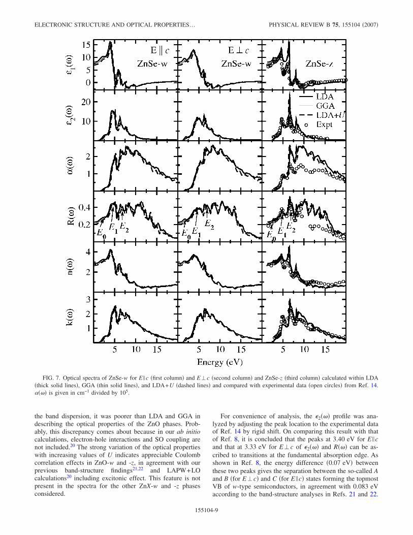
FIG. 7. Optical spectra of ZnSe-w for E �c �first column� and E�c �second column� and ZnSe-z �third column� calculated within LDA�thick solid lines�, GGA �thin solid lines�, and LDA+U �dashed lines� and compared with experimental data �open circles� from Ref. 14.���� is given in cm−1 divided by 105.
ELECTRONIC STRUCTURE AND OPTICAL PROPERTIES… PHYSICAL REVIEW B 75, 155104 �2007�
155104-9

There are two broad shoulders of the peak E0 located at4.44 and 5.90 eV for E�c and 3.90 and 5.29 eV for E �c.Similar shoulders are found at lower energies in the experi-mental spectra of Refs. 8 and 82 observed at 3.35 and3.41 eV for E�c and 3.39 and 3.45 eV for E �c, and theorigin of these shoulders has been ascribed to exciton-phonon coupling. However, in our ab initio studies, excitonsand lattice vibrations are not taken into consideration.
D. ZnS-w and ZnS-z
The experimental14 optical spectra for the ZnS-w and -zphases are displayed in Fig. 6, together with those calculated
according to the LDA, GGA, and LDA+U. It is seen that themagnitudes of the experimentally11 observed shouldersaround the E2 peak in the reflectivity spectra of ZnS-w areoverestimated in the DFT calculations. As a result, the inten-sities of the shoulders are almost the same as the intensitiesof the peaks E1 and E2 for E�c and even exceeds them forE �c.
The calculated optical spectra for ZnS-w by LDA, GGA,and LDA+U turned out to be almost identical at energiesbelow 10 eV. However, at higher energies, the LDA- andGGA-derived peaks differ from those obtained by LDA+U.This difference can be associated with Zn 3d electrons,
FIG. 8. Optical spectra of ZnTe-w for E �c �first column� and E�c �second column� and ZnTe-z �third column� calculated within LDA�thick solid lines�, GGA �thin solid lines�, and LDA+U �dashed lines� and compared with experimental data �open circles� from Ref. 14.���� is given in cm−1 divided by 105.
KARAZHANOV et al. PHYSICAL REVIEW B 75, 155104 �2007�
155104-10

which were shifted toward lower energies in the LDA+Ucalculations. Hence, in ZnS-w and -z, the Coulomb correla-tion effects appear to play a significant role in optical prop-erties at energies higher than 10 eV.
Compared to ZnO-w, the calculated optical spectra ofZnS-w and -z show larger disagreement with the experimen-tal data. The discrepancy is quite pronounced in the absorp-tion and reflectivity spectra of ZnS-w and -z, especially atenergies exceeding 7 eV. The magnitude of the peaks locatedat higher energies are overestimated significantly comparedto the experimental data. The overestimation is more severein ZnS-z than in ZnS-w as judged from the intensity of theE2 peak.
E. ZnSe-w, ZnTe-w, ZnSe-z, and ZnSe-z
The optical spectra for ZnSe-w, ZnSe-z, ZnTe-w, andZnTe-z calculated by DFT within LDA, GGA, and LDA+U are displayed in Figs. 7 and 8, together with the corre-sponding experimental spectra. Since experimental opticalspectra for ZnSe-w and ZnTe-w are not available, rigid shiftof the parameters toward higher energies has been performedon the basis of the reflectivity spectra for ZnSe-z and ZnTe-z�Figs. 7 and 8�. A closer inspection of Figs. 7 and 8 showsthat the optical spectra calculated within LDA, GGA, andLDA+U are almost the same for all selenide and telluridephases. The small differences noted in the absorption andreflectivity spectra appear to originate from the Zn 3delectrons.
The location and magnitude of the experimentally mea-sured E1 peak in the reflectivity spectra of ZnSe-z andZnTe-z have been assigned14,11 to fundamental absorptionand 3− 1 transitions at the �0.17,0.17,0.17� point of theBrillouin zone. These assignments agree well with theoreti-cal calculations. However, the theoretical calculations did notlocate the E1+�1 peak on the high-energy side of the E1peak, which was observed experimentally for both ZnSe-zand ZnTe-z. The reason is certainly that SO coupling was notincluded in the calculations.
The experimental13 E0 peak in the reflectivity spectra, cor-responding to transitions at k=0 �viz., from the highest stateof VB ��15� to the lowest state of CB ��1��, is well repro-duced by the theoretical calculations. One also sees the E0+�0 peak in the theoretical spectra, which was previously13
ascribed to SO splitting. Since SO coupling was neglected inthe theoretical calculations, the origin of the E0+�0 peak isnot likely to be related to SO coupling.
Similar to the findings for ZnS-z, the theoretically calcu-lated optical spectra for the lower-energy regions of ZnSe-zand ZnTe-z agree with experimental findings. However, theintensity of the peaks located at higher energies is overesti-mated in the DFT calculations. Anyway, this discrepancy isnot as severe as that for ZnS-z. The calculated reflectivityspectra agree well with experimental data in the energy range�6 eV. At higher energies �6–15 eV�, LDA, GGA, andLDA+U all overestimate the intensity of the reflectivity.Fairly good agreement with the experimental data isachieved in the energy range 15–20 eV for the real andimaginary parts of the dielectric function for ZnSe-z and
ZnTe-z. For the other optical spectra of ZnSe-z and ZnTe-z,the agreement between theory and experiment is poorer.
F. Influence of spin-orbit splitting on the opticalspectra of ZnX
It is well known that SO splitting at the top of the VB ofa semiconductor is very important for optical transitions, andone should expect large difference in the optical spectra cal-culated with and without the SO coupling. In this section, weshall analyze how the SO coupling influences the opticalspectra of ZnX. For this analysis, ab initio band-structurecalculations have been performed using the MINDLAB soft-ware with and without SO coupling. Based on the band-structure studies, the dielectric-response function �2��� hasbeen calculated. The results for ZnX-z are presented in Fig. 9and compared with experimental data, where it is seen that�2��� calculated for ZnO-z without SO coupling is slightlyhigher than that with the SO coupling, with the main devia-tions occurring at 3.44–6.00 and 10.00–12.00 eV. The rea-son for the small distinctions in �2��� in this case is the smallSO splitting energy.
Our findings show that the SO splitting influences thecalculated optical spectra and, in particular, it is most pro-nounced at energies lower than �12 eV. At higher energies,the difference between the optical spectra calculated withand without SO coupling is fairly small and agrees reason-ably well with the experimental data.14 This statement ap-plies to all ZnX phases studied. It should be noted that inten-sities of the peaks calculated with SO coupling are generallylower than those obtained without SO coupling and the latterset agrees better with the experimental data than the former.Furthermore, in the experimental spectra, there are low in-tensity peaks located at 9.4 eV in ZnS-z, 8.4 eV in ZnS-z,and 7.0 eV in ZnTe-z. However, these peaks are not seen inthe calculated spectra with the SO coupling. As noted, thisdiscrepancy can be related to the neglect of many of theabove factors such as Coulomb interaction between electronsand holes, local-field effects, and indirect transitions etc.
G. Role of the ground-state structurein the optical spectra of ZnX
In this section, we shall analyze optical spectra of ZnXcalculated using the experimentally and theoretically deter-mined lattice parameters. To find the lattice parameters fromthe ab initio calculations, the structural optimization hasbeen performed, which includes the following steps: atomsare relaxed keeping the volume and shape of the lattice. Afterconvergence is reached, the resulting lattice and positionalparameters have been used as input to optimize atomic posi-tions, shape, and volume of the unit cell altogether. Then,dependence of the total energy on volume is studied. Theminimum of the dependence was accepted as the equilibriumstate. Lattice and positional parameters corresponding to theminimum are referred to as the theoretically determined lat-tice parameters. The thus determined theoretical lattice pa-rameters do not deviate much from the experimental ones.These parameters along with the experimentally determined
ELECTRONIC STRUCTURE AND OPTICAL PROPERTIES… PHYSICAL REVIEW B 75, 155104 �2007�
155104-11

ones were used for subsequent computations of the elec-tronic structure and optical spectra. The results are presentedin Fig. 10 for ZnX-w for E�. Analysis shows that the opticalspectra of ZnO-w for E� deviate from each other at energiesnear the fundamental absorption and at higher energies in therange 8–13 eV. The reason for the difference can be relatedto changes of the p-d coupling because of the changes of theZn-O bond lengths coming from structural optimization. Op-tical spectra of ZnO-w for E �c and those of other ZnX-w and-z calculated using the theoretical and experimental latticeparameters do not differ from each other significantly.
IV. CONCLUSION
The band structures of the ZnX-w and -z phases �X=O, S,Se, and Te� are calculated by DFT within LDA, GGA, and
LDA+U. The topmost VB states are found to be more dis-persive than the bottommost CB states. Spin-orbit couplingis found to play an important role for band dispersion, loca-tion, and width of the Zn 3d band and the lowest s band. Byanalyzing the dependence of the band gaps on the atomicnumber of X for ZnX, the band gap of ZnO-z is estimated tobe �3.3 eV. Using the electronic band structures as refer-ences, the optical spectra of ZnX-w and -z are analyzed in theenergy range 0–20 eV. The locations of the peaks corre-sponding to transitions at the fundamental absorption edgecalculated by DFT are shifted to lower energies relative tothe experimental peaks. This deficiency originates from thewell-known errors in band gaps calculated according to DFT.In order to correct the underestimation of band gaps calcu-lated by DFT, the location of the calculated peaks of theoptical spectra has been rigidly shifted toward higher ener-gies to match the experimentally determined locations. In the
FIG. 9. Imaginary part of the dielectric-response function �2���for ZnO-z, ZnS-z, ZnSe-z, and ZnTe-z calculated by DFT using theMINDLAB package within LDA, including SO coupling into consid-eration �dashed lines�, and without SO coupling �continuous lines�,and compared to experimental data �open circles� from Ref. 14.
FIG. 10. Imaginary part of the dielectric-response function�2��� for ZnX-z calculated by VASP-PAW package using the theo-retically �solid lines� and experimentally �open circles� determinedlattice parameters.
KARAZHANOV et al. PHYSICAL REVIEW B 75, 155104 �2007�
155104-12

thus obtained spectra, the locations of the peaks in the lower-energy region agree well with the experimental data. How-ever, the peaks in the higher-energy region agree only toler-ably well with the experimental findings. The overallconclusion is that the k-independent scissors operator pro-vides a good first approximation for correlation of the under-estimated band gaps for the ZnX-w and -z phases. Based onthis result, “corrected� band structures of the ZnX phases arearranged by adjusting the band gap up to experimentallymeasured value �viz., rigidly lifting the lowest CB�. Not onlythe locations but also the intensities of some of the calculatedlow-energy peaks agree with available experimental data forall ZnX phases. However, the intensities of some peaks lo-cated at higher energies and shoulders have been overesti-mated. The GGA approach slightly improved the band-gapvalues. Also, the optical spectra of ZnO-w for E�c calcu-lated within the GGA agree better with the experimental datathan those calculated within the LDA and LDA+U ap-proaches. The value for the corresponding transition at thefundamental absorption edge is decreased and becomessharper with the use of the GGA, thus providing better agree-ment with experimental data than LDA. For E�c, inhomo-geneity in the electron gas plays an important role, while it is
not so important for E �c. The optical spectra for ZnO-w and-z calculated within LDA+U for the energy range 0–20 eVare found to depend significantly on the location of the en-ergy levels of the Zn 3d electrons. For the other ZnX-w and-z phases, such changes are not so pronounced, in fact, onlynoticeable at energies above 10 eV. Strong Coulomb corre-lation effects are established for ZnO-w and -z. According tothe present LDA+U calculations, the probability for the op-tical transitions at the fundamental absorption edge ofZnO-w and -z decreases with increasing U. Optical spectrafor ZnO-z, ZnSe-w, and ZnTe-w have been predicted. Theinfluence of the spin-orbit coupling is found to increase withincreasing the atomic number of the X component of ZnX.
ACKNOWLEDGMENTS
This work has received financial and supercomputing sup-port from the Research Council of Norway and Academy ofSciences of Uzbekistan �Project No. N31-36,24-06�. The au-thors are thankful to R. Vidya for critical reading of themanuscript and comments. We also thank P. Vajeeston, A.Klaveness, and Dr. K. Knizek for computation-practical help.
1 H. Yoshikawa and S. Adachi, Jpn. J. Appl. Phys., Part 1 36, 6237�1997�.
2 K. Postava, H. Sueki, M. Aoyama, T. Yamaguchi, C. Ino, Y.Igasaki, and M. Horie, J. Appl. Phys. 87, 7820 �2000�.
3 K. Postava, H. Sueki, M. Aoyama, T. Yamaguchi, K. Murakami,and Y. Igasaki, Appl. Surf. Sci. 175-176, 543 �2001�.
4 P. L. Washington, H. C. Ong, J. Y. Dai, and R. Chang, Appl. Phys.Lett. 72, 3261 �2000�.
5 J. F. Muth, R. M. Kolbas, A. K. Sharma, S. Oktyabrsky, and J.Narayan, J. Appl. Phys. 85, 7884 �1999�.
6 V. Srikant and D. R. Clarke, J. Appl. Phys. 83, 5447 �1998�.7 R. L. Hengehold, R. J. Almassy, and F. L. Pedrotti, Phys. Rev. B
1, 4784 �1970�.8 R. Klucker, H. Nelkowski, Y. S. Park, M. Skibowski, and T. S.
Wagner, Phys. Status Solidi B 45, 265 �1971�.9 J. L. Freeouf, Phys. Rev. B 7, 3810 �1973�.
10 M. Cardona and R. Haensel, Phys. Rev. B 1, 2605 �1970�.11 M. Cardona and G. Harbeke, Phys. Rev. 137, A1467 �1965�.12 A. E. Merad, M. B. Kanoun, G. Merad, J. Cibert, and H. Aourag,
Mater. Chem. Phys. 92, 333 �2005�.13 M. Cardona and D. L. Greenaway, Phys. Rev. 131, 98 �1963�.14 Optical Constants of Crystalline and Amorphous Semiconduc-
tors: Numerical Data and Graphical Information, edited by S.Adachi �Kluwer Academic, Boston, 1999�.
15 V. V. Sobolev and V. V. Sobolev, Phys. Low-Dimens. Semicond.Struct. 9/10, 113 �2003�.
16 P. Hohenberg and W. Kohn, Phys. Rev. 136, B864 �1964�.17 W. Kohn and L. J. Sham, Phys. Rev. 140, A1133 �1965�.18 Y.-N. Xu and W. Y. Ching, Phys. Rev. B 48, 4335 �1993�.19 C. S. Wang and B. M. Klein, Phys. Rev. B 24, 3417 �1981�.20 R. Laskowski and N. E. Christensen, Phys. Rev. B 73, 045201
�2006�.
21 S. Z. Karazhanov, P. Ravindran, U. Grossner, A. Kjekshus, H.Fjellvåg, and B. G. Svensson, J. Appl. Phys. 100, 043709�2006�.
22 S. Z. Karazhanov, P. Ravindran, U. Grossner, A. Kjekshus, H.Fjellvåg, and B. G. Svensson, J. Cryst. Growth 287, 162 �2006�.
23 V. I. Anisimov, I. V. Solovyev, M. A. Korotin, M. T. Czyzyk, andG. A. Sawatzky, Phys. Rev. B 48, 16929 �1993�.
24 S. L. Dudarev, G. A. Botton, S. Y. Savrasov, C. J. Humphreys,and A. P. Sutton, Phys. Rev. B 57, 1505 �1998�.
25 O. Bengone, M. Alouani, P. Blöchl, and J. Hugel, Phys. Rev. B62, 16392 �2000�.
26 W. R. L. Lambrecht, A. V. Rodina, S. Limpijumnong, B. Segall,and B. K. Meyer, Phys. Rev. B 65, 075207 �2002�.
27 L. C. Lew Yan Voon, M. Willatzen, M. Cardona, and N. E. Chris-tensen, Phys. Rev. B 53, 10703 �1996�.
28 P. Carrier and S.-H. Wei, Phys. Rev. B 70, 035212 �2004�.29 S.-H. Wei and A. Zunger, Appl. Phys. Lett. 69, 2719 �1996�.30 M. Willatzen, M. Cardona, and N. E. Christensen, Phys. Rev. B
51, 17992 �1995�.31 S. Lalitha, S. Z. Karazhanov, P. Ravindran, S. Senthilarasu, R.
Sathyamoorthy, and J. Janabergenov, Physica B 387, 227�2006�.
32 R. F. W. Bader, Atoms in Molecules: A Quantum Theory �OxfordUniversity Press, New York, 1990�.
33 M. Cardona, N. E. Christensen, and G. Fasol, Phys. Rev. B 38,1806 �1995�.
34 M. Usuda, N. Hamada, T. Kotani, and M. van Schilfgaarde, Phys.Rev. B 66, 125101 �2002�.
35 M. Oshikiri and F. Aryasetiawan, J. Phys. Soc. Jpn. 69, 2113�2000�.
36 A. Fleszar and W. Hanke, Phys. Rev. B 71, 045207 �2005�.37 P. Rinke, A. Qteish, J. Neugebauer, C. Freysoldt, and M. Schef-
ELECTRONIC STRUCTURE AND OPTICAL PROPERTIES… PHYSICAL REVIEW B 75, 155104 �2007�
155104-13

fler, New J. Phys. 7, 126 �2005�.38 M. Städele, M. Moukara, J. A. Majewski, P. Vogl, and A. Görling,
Phys. Rev. B 59, 10031 �1999�.39 S. Sharma, J. K. Dewhurst, and C. Ambrosch-Draxl, Phys. Rev.
Lett. 95, 136402 �2005�.40 R. Asahi, W. Mannstadt, and A. J. Freeman, Phys. Rev. B 59,
7486 �1999�.41 L. X. Benedict, E. L. Shirley, and R. B. Bohn, Phys. Rev. B 57,
R9385 �1998�.42 F. Bechstedt, K. Tenelsen, B. Adolph, and R. Del Sole, Phys. Rev.
Lett. 78, 1528 �1997�.43 G. A. Baraff and M. Schlüter, Phys. Rev. B 30, 3460 �1984�.44 A. Delin, P. Ravindran, O. Eriksson, and J. M. Wills, Int. J. Quan-
tum Chem. 69, 349 �1998�.45 P. Ravindran, A. Delin, B. Johansson, O. Eriksson, and J. M.
Wills, Phys. Rev. B 59, 1776 �1999�.46 Inorganic Crystal Structure Database �Gmelin Institut, Karlsruhe,
2001�.47 Handbook of Laser Science and Technology, edited by M. J. We-
ber �CRC, Cleveland, 1986�, Vol. III.48 O. Zakharov, A. Rubio, X. Blase, M. L. Cohen, and S. G. Louie,
Phys. Rev. B 50, 10780 �1994�.49 N. Lakshmi, N. M. Rao, R. Venugopal, D. R. Reddy, and B. K.
Reddy, Mater. Chem. Phys. 82, 764 �2003�.50 V. N. Tomashik, G. S. Oleinik, and I. B. Mizetskaya, Inorg.
Mater. 14, 1119 �1978�.51 W. H. Bragg and J. A. Darbyshire, J. Met. 6, 238 �1954�.52 Semiconductors: Physics of Group IV Elements and III-V Com-
pounds, edited by K.-H. Hellwege and O. Madelung, Landolt-Boörnstein, New series, Group III, Vol. 17, Pt. A �Springer-Verlag, Berlin, 1982�; Theoretical Structures of Molecules,edited by P. von Ragué Schleyer, Landolt-Börnstein, New Se-ries, Group II, Vol. 22, Pt. A �Springer-Verlag, Berlin, 1993�.
53 CRC Handbook of Chemistry and Physics, 70th ed., edited by R.C. Weast, D. R. Lide, M. J. Astle, and W. H. Beyer �CRC, BocaRaton, FL,1990�.
54 B. K. Agrawal, P. S. Yadav, and S. Agrawal, Phys. Rev. B 50,14881 �1994�.
55 G. Kresse and J. Furthmüller, Phys. Rev. B 54, 11169 �1996�.56 J. P. Perdew, K. Burke, and M. Ernzerhof, Phys. Rev. Lett. 77,
3865 �1996�.57 J. P. Perdew and A. Zunger, Phys. Rev. B 23, 5048 �1981�.58 D. M. Ceperley and B. J. Alder, Phys. Rev. Lett. 45, 566 �1980�.59 P. E. Blöchl, Phys. Rev. B 50, 17953 �1994�.
60 G. Kresse and D. Joubert, Phys. Rev. B 59, 1758 �1999�.61 B. Adolph, J. Furthmüller, and F. Bechstedt, Phys. Rev. B 63,
125108 �2001�.62 D. Vogel, P. Krüger, and J. Pollmann, Phys. Rev. B 52, R14316
�1995�.63 C. L. Dong, C. Persson, L. Vayssieres, A. Augustsson, T. Schmitt,
M. Mattesini, R. Ahuja, C. L. Chang, and J.-H. Guo, Phys. Rev.B 70, 195325 �2004�.
64 A. Janotti and C. G. Van de Walle, J. Cryst. Growth 287, 58�2006�.
65 W. E. Pickett, S. C. Erwin, and E. C. Ethridge, Phys. Rev. B 58,1201 �1998�.
66 M. Ruckh, D. Schmid, and H. W. Schock, J. Appl. Phys. 76, 5945�1994�.
67 S. Y. Savrasov, Phys. Rev. B 54, 16470 �1996�.68 O. Gunnarsson and B. I. Lundqvist, Phys. Rev. B 13, 4274
�1976�.69 S. H. Vosko, L. Wilk, and M. Nusair, Can. J. Phys. 58, 1200
�1980�.70 P. Ravindran, A. Delin, R. Ahuja, B. Johansson, S. Auluck, J. M.
Wills, and O. Eriksson, Phys. Rev. B 56, 6851 �1997�.71 P. Ravindran, A. Delin, P. James, B. Johansson, J. M. Wills, R.
Ahuja, and O. Eriksson, Phys. Rev. B 59, 15680 �1999�.72 D. Vogel, P. Krüger, and J. Pollmann, Phys. Rev. B 54, 5495
�1996�.73 Semiconductors: Other than Group IV Elements and IV Elements
and III-V Compounds, edited by O. Madelung �Springer, Berlin,1992�.
74 K. Hümmer, Phys. Status Solidi B, 56, 249 �1973�.75 J. J. Hopfield, J. Phys. Chem. Solids 15, 97 �1960�.76 S.-H. Wei and A. Zunger, Phys. Rev. B 39, 3279 �1989�.77 S.-H. Wei and A. Zunger, Phys. Rev. B 37, 8958 �1988�.78 Semiconductors: Physics of Group IV Elements and III-V Com-
pounds, edited by O. Madelung, M. Schulz, and H. Weiss,Landolt-Bömstein, New Series, Group III, Vol. 17, Pt. A�Springer, Berlin, 1982�.
79 Semiconductors: Basic Data, 2nd ed., edited by O. Madelung�Springer, Berlin, 1996�.
80 A. Mang, K. Reimann, and S. Rübenacke, Solid State Commun.94, 251 �1995�.
81 M. L. Cohen and J. R. Chelikowsky, Electronic Structure andOptical Properties of Semiconductors �Springer, Berlin, 1988�.
82 W. Y. Liang and A. D. Yoffe, Phys. Rev. Lett. 20, 59 �1968�.
KARAZHANOV et al. PHYSICAL REVIEW B 75, 155104 �2007�
155104-14